P4KE530 AND P4KE550
TRANSZORB™ TRANSIENT VOLTAGE SUPPRESSOR
Steady State Power - 1Watt Reverse Voltage - 530, 550 Volts
FEATURES
♦ Plastic package has Underwriters Laboratory
Flammability Classification 94V-0
♦ Protects TOPSwitch
®
♦ Glass Passivated Junction
♦ High temperature soldering guaranteed:
250°C/10 seconds at terminals
♦ Exellent Clamping capability
♦ Available in unidirectional only
MECHANICAL DATA
Case: JEDEC DO-204AL molded plastic body over
passivated junction
Terminals: Axial leads, solderable per MIL-STD-750,
Method 2026
Polarity: The color band denotes the cathode, which is
positive with respect to the anode under normal TVS
operation
Mounting Position: Any
Weight: 0.012 ounce, 0.3 gram
MAXIMUM RATINGS AND ELECTRICAL CHARACTERISTICS
Ratings at 25°C ambient temperature unless otherwise specified.
SYMBOLS P4KE530 P4KE550 UNITS
Steady state power dissipation
(NOTE 3)
P
M(AV)
1.0 Watts
Peak pulse power dissipation
(NOTE 1,2, FIG.1)
P
PPM
Minimum 300 Watts
Minimum breakdown voltage at 100µAV
(BR)
530 550 Volts
Maximum clamping voltage at 300mA, 10/1000 µs
-
waveform Vc 660 Volts
Stand-off voltage V
WM
477 495 Volts
Maximum DC reverse leakage current at V
WM
I
D
5.0 µA
Typical temperature coefficient of V
(BR)
650 mV°C
Typical capacitance
(NOTE 4)
at 0V
C
J
75
pF
at 200V 45
Operating junction and storage temperature range T
J
, T
STG
-55 to +150 °C
NOTES:
(1) Non-repetitive current pulse, per Fig.3 and derated above 25°C per - Fig. 2
(2) Peak pulse power waveform is 10/100µS
(3) Lead temperature at 75°C=T
L
(4) Measured at 1MHz
1/20/99
ADVANCED INFORMATION
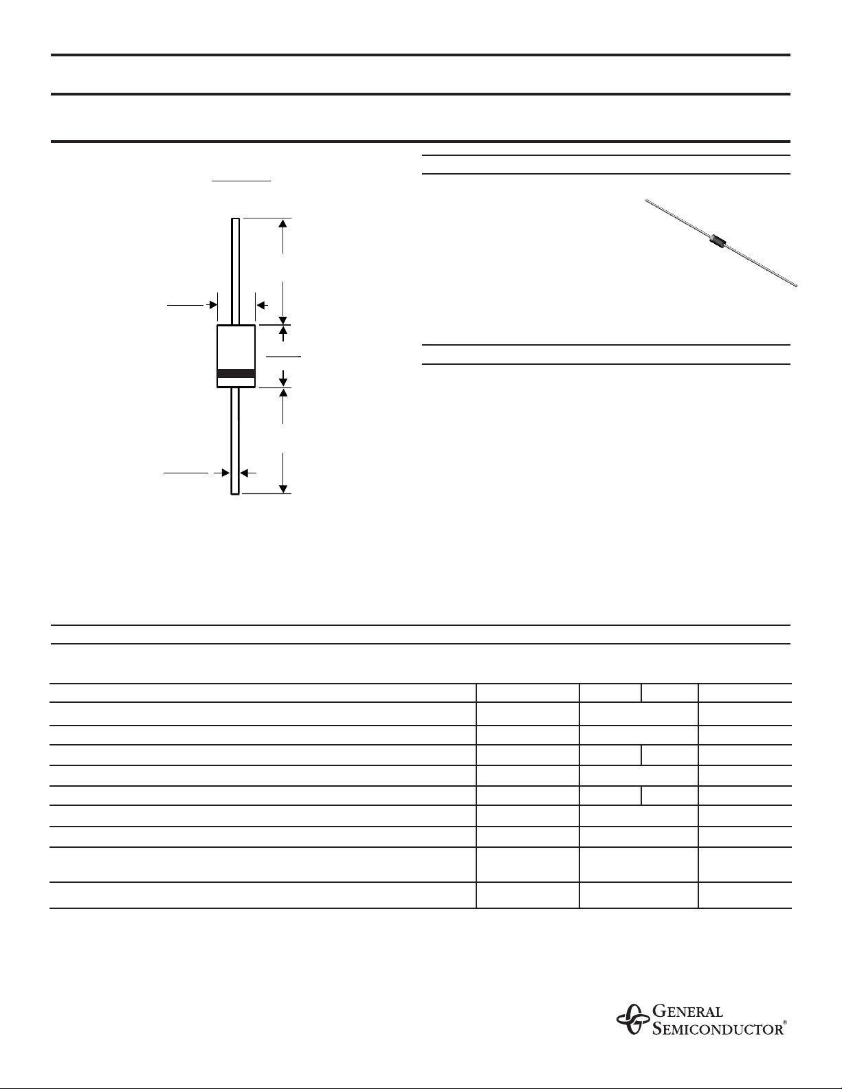
Dimensions are in inches and (millimeters)
Available in uni-directional only
DO-204AL
1.0 (25.4)
MIN.
0.107 (2.7)
0.080 (2.0)
DIA.
0.205 (5.2)
0.160 (4.1)
1.0 (25.4)
MIN.
0.034 (0.86)
0.028 (0.71)
DIA.

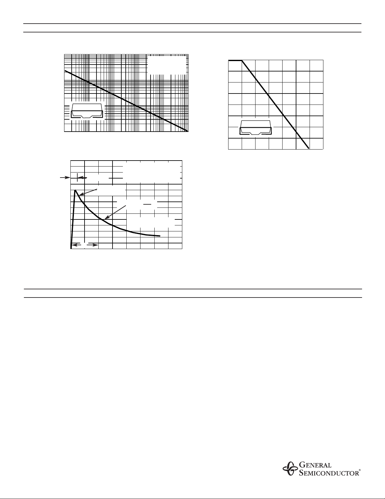
MAXIMUM RATINGS AND CHARACTERISTIC CURVES P4KE530 AND P4KE550
FIG. 1 - PEAK PULSE POWER RATING CURVE
P
PPM
, PEAK PULSE POWER, kW
td, PULSE WIDTH, sec.
TA, AMBIENT TEMPERATURE, °C
FIG. 3 - PULSE WAVEFORM
t, TIME, ms
I
PPM,
PEAK PULSE CURRENT, %
PEAK PULSE POWER (Ppp) or CURRENT (
IPPM
)
DERATING IN PERCENTAGE, %
NON-REPETITIVE
PULSE WAVEFORM
SHOWN in FIG. 3
TA=25°C
PULSE WIDTH (td) is DEFINED
as the POINT WHERE the PEAK
CURRENT DECAYS
to 50% of I
PPM
tr=10µsec.
td
PEAK VALUE
I
PPM
HALF VALUE - I
PPM
2
10/1000µsec. WAVEFORM
as DEFINED by R.E.A.
FIG. 2 - PULSE DERATING CURVE
♦
Respect Thermal Resistance (PCB Layout) - as the temperature coefficient also
contributes to the clamping voltage.
♦
Select minimum breakdown voltage, so you get acceptable power dissipation and
PCB tie point temperature. Devices with higher breakdown voltage will have a
shorter conduction time and will dissipate less power.
♦
Clamping voltage is influenced by internal resistance - design approximation is
7V per 100mA slope.
♦
Keep temperature of TVS lower than TOPSwitchas a recommendation.
♦
Maximum current is determined by the maximum TJand can be higher than
300mA. Contact supplier for different clamping voltage / current arrangements.
♦
Minimum breakdown voltage can be customized for other applications.
Contact supplier.
APPLICATION NOTES
100
10
1.0
0.1
0.1
µ
s
1.0
µ
s
150
100
50
0
0
1.0
10
µ
s
100
µ
s
2.0
1.0ms 10ms
3.0
4.0
10,000
100
1,000
75
50
25
0
25
0
50
75
100
125
150
175
 Loading...