

Datasheet P4KE10, P4KE100CA, P4KE11, P4KE110C, P4KE11CA Datasheet (SHANGHAI SUNRISE ELECTRONICS CO)
...
SHANGHAI SUNRISE ELECTRONICS CO., LTD.
µ
)
(BR)
(BR)
P4KE6.8 THRU P4KE440CA
TRANSIENT VOLTAGE SUPPRESSOR
BREAKDOWN VOLTAGE:6.8-440V
PEAK PULSE POWER: 400W
TECHNICAL
SPECIFICATION
FEATURES
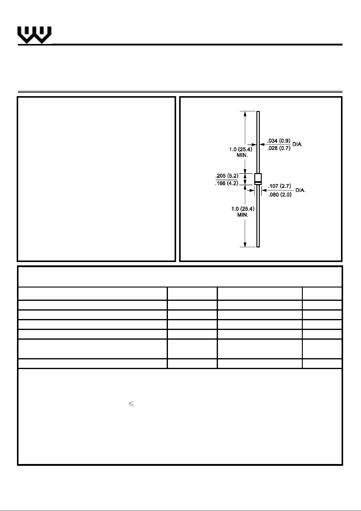
DO - 41
• 400W peak pulse power capability
• Excellent clamping capability
• Low incremental surge resistance
• Fast response time:
typically less than 1.0ps from 0V to V
BR
for unidirectional and 5.0nS for bidirectional types.
• High temperature soldering guaranteed:
o
265
C/10S/9.5mm lead length at 5 lbs tension
MECHANICAL DATA
• Terminal: Plated axial leads solderable per
MIL-STD 202E, method 208C
• Case: Molded with UL-94 Class V-O recognized
flame retardant epoxy
• Polarity: Color band denotes cathode except for
unidirectional types.
Dimensions in inches and (millimeters)
• Mounting position: Any
MAXIMUM RATINGS AND ELECTRICAL CHARACTERISTICS
(Ratings at 25oC ambient temperature unless otherwise specified)
RATINGS
Peak power dissipation (Note 1) Pppm Minimum 400 W
Peak pulse reverse current (Note 1) Ippm See Table A
Steady state power dissipation (Note 2) Pm(av) 1.0 W
Peak forward surge current (Note 3)
Maximum instantaneous forward voltage at 50A
for unidirectional only (Note 4)
Operating junction and storage temperature range
Notes:
1. 10/1000
2. Tl=75
3. Measured on 8.3ms single half sine-wave or equivalent square wave,duty cycle=4 pulses per minute maximum.
4. V
DEVICES FOR BIDIRECTIONAL APPLICATIONS
1. Suffix 'A' dnotes 5% tolerance device,no suffix 'A' dnotes 10% tolerance device.
2. For bidirectional use 'C' or 'CA' suffix for types P4KE7.5 thru types P4KE440A
(e.g. P4KE7.5C,P4KE440CA), for unidirectional don't use 'C' suffix after types.
3. For bidirectional devices having V
4. Electrical characteristics apply in both directions.
=3.5V max. for devices of V
F
S waveform non-repetitive current pulse, and derated above Ta=25oC
o
C, lead length 9.5mm, Mounted on copper pad area of (40×40mm
200V, and VF=5.0V max. for devices of V
of 10 volts and less, the ID limit is doubled.
WM
SYMBOL VALUE UNITS
I
FSM
V
T
STG,TJ
F
40 A
3.5/6.5 V
-55 to + 175
>200V
o
C
http://www.sse-diode.com
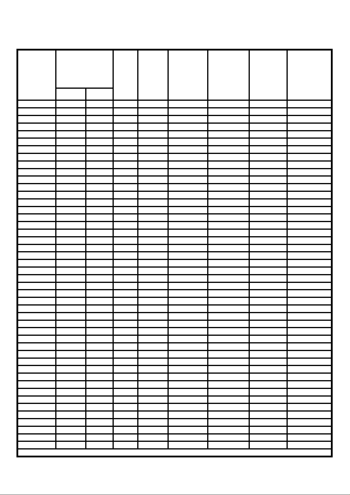
ELECTRICAL CHARACTERISTICS
( at TA=25oC unless otherwise noted )
Breakdown
Voltage V
Device Type
(Volts)
(NOTE 1)
MIN MAX
*P4KE6.8
*P4KE6.8A
P4KE7.5
P4KE7.5A
P4KE8.2
P4KE8.2A
P4KE9.1
P4KE9.1A
P4KE10
P4KE10A
P4KE11
P4KE11A
P4KE12
P4KE12A
P4KE13
P4KE13A
P4KE15
P4KE15A
P4KE16
P4KE16A
P4KE18
P4KE18A
P4KE20
P4KE20A
P4KE22
P4KE22A
P4KE24
P4KE24A
P4KE27
P4KE27A
P4KE30
P4KE30A
P4KE33
P4KE33A
P4KE36
P4KE36A
P4KE39
P4KE39A
P4KE43
P4KE43A
P4KE47
P4KE47A
P4KE51
P4KE51A
P4KE56
P4KE56A
* Not available as bidirectional devices
6.12 7.48 10.0 5.50 1000.0 38.0 10.8 0.057
6.45 7.14 10.0 5.80 1000.0 40.0 10.5 0.057
6.75 8.25 10.0 6.05 500.0 36.0 11.7 0.061
7.13 7.88 10.0 6.40 500.0 37.0 11.3 0.061
7.38 9.02 10.0 6.63 200.0 33.0 12.5 0.065
7.79 8.61 10.0 7.02 200.0 35.0 12.1 0.065
8.19 10.0 1.0 7.37 50.0 30.0 13.8 0.068
8.65 9.55 1.0 7.78 50.0 31.0 13.4 0.068
9.00 11.0 1.0 8.10 10.0 28.0 15.0 0.073
9.50 10.5 1.0 8.55 10.0 29.0 14.5 0.073
9.90 12.1 1.0 8.92 5.0 26.0 16.2 0.075
10.5 11.6 1.0 9.40 5.0 27.0 15.6 0.075
10.8 13.2 1.0 9.72 5.0 24.0 17.3 0.078
11.4 12.6 1.0 10.2 5.0 25.0 16.7 0.078
11.7 14.3 1.0 10.5 5.0 22.0 19.0 0.081
12.4 13.7 1.0 11.1 5.0 23.0 18.2 0.081
13.5 16.5 1.0 12.1 5.0 19.0 22.0 0.084
14.3 15.8 1.0 12.8 5.0 20.0 21.2 0.084
14.4 17.6 1.0 12.9 5.0 18.0 23.5 0.086
15.2 16.8 1.0 13.6 5.0 19.0 22.5 0.086
16.2 19.8 1.0 14.5 5.0 16.0 26.5 0.088
17.1 18.9 1.0 15.3 5.0 17.0 25.2 0.088
18.0 22.0 1.0 16.2 5.0 14.0 29.1 0.090
19.0 21.0 1.0 17.1 5.0 15.0 27.7 0.090
19.8 24.2 1.0 17.8 5.0 13.0 31.9 0.092
20.9 23.1 1.0 18.8 5.0 14.0 30.6 0.092
21.6 26.4 1.0 19.4 5.0 12.0 34.7 0.094
22.8 25.2 1.0 20.5 5.0 13.0 33.2 0.094
24.3 29.7 1.0 21.8 5.0 11.0 39.1 0.096
25.7 28.4 1.0 23.1 5.0 11.2 37.5 0.096
27.0 33.0 1.0 24.3 5.0 10.0 43.5 0.097
28.5 31.5 1.0 25.6 5.0 10.0 41.4 0.097
29.7 36.3 1.0 26.8 5.0 9.0 47.7 0.098
31.4 34.7 1.0 28.2 5.0 9.0 45.7 0.098
32.4 39.6 1.0 29.1 5.0 8.0 52.0 0.099
34.2 37.8 1.0 30.8 5.0 8.4 49.9 0.099
35.1 42.9 1.0 31.6 5.0 7.4 56.4 0.100
37.1 41.0 1.0 33.3 5.0 7.8 53.9 0.100
38.7 47.3 1.0 34.8 5.0 6.8 61.9 0.101
40.9 45.2 1.0 36.8 5.0 7.1 59.3 0.101
42.3 51.7 1.0 38.1 5.0 6.2 67.8 0.101
44.7 49.4 1.0 40.2 5.0 5.0 64.8 0.101
45.9 56.1 1.0 41.3 5.0 5.7 73.5 0.102
48.5 53.6 1.0 43.6 5.0 6.0 70.1 0.102
50.4 61.6 1.0 45.4 5.0 5.2 80.5 0.103
53.2 58.8 1.0 47.8 5.0 5.5 77.0 0.103
(BR)
Current
I
Test
(mA)
T
Stand-off
Voltage
V
WM
(Volts)
Maximum
Reverse
Leakage at
WM ID
(µA)
V
(NOTE 3)
Maximum
Peak Pulse
Reverse
Current I
ppm
(Amps)
(NOTE 2)
Maximum
Clamping
Voltage at
I
ppm VC
(Volts)
Maximum
Temperature
Coefficient of
(%/oC)
V
(BR)
http://www.sse-diode.com

(BR)
ELECTRICAL CHARACTERISTICS
( at TA=25oC unless otherwise noted )
Breakdown
Voltage V
Device Type
(Volts)
(NOTE 1)
MIN MAX
P4KE62
P4KE62A
P4KE68
P4KE68A
P4KE75
P4KE75A
P4KE82
P4KE82A
P4KE91
P4KE91A
P4KE100
P4KE100A
P4KE110
P4KE110A
P4KE120
P4KE120A
P4KE130
P4KE130A
P4KE150
P4KE150A
P4KE160
P4KE160A
P4KE170
P4KE170A
P4KE180
P4KE180A
P4KE200
P4KE200A
P4KE220
P4KE220A
P4KE250
P4KE250A
P4KE300
P4KE300A
P4KE350
P4KE350A
P4KE400
P4KE400A
P4KE440
P4KE440A
NOTES:
1. V
2. Surge current waveform and derated
3. For bidirectional types having V
55.8 68.2 1.0 50.2 5.0 4.7 89.0 0.104
58.9 65.1 1.0 53.0 5.0 5.0 85.0 0.104
61.2 74.8 1.0 55.1 5.0 4.3 98.0 0.104
64.6 71.4 1.0 58.1 5.0 4.6 92.0 0.104
67.5 82.5 1.0 60.7 5.0 3.9 108.0 0.105
71.3 78.8 1.0 64.1 5.0 4.1 103.0 0.105
73.8 90.2 1.0 66.4 5.0 3.6 118.0 0.105
77.9 86.1 1.0 70.1 5.0 3.7 113.0 0.105
81.9 100 1.0 73.7 5.0 3.2 131.0 0.106
86.5 95.5 1.0 77.8 5.0 3.4 125.0 0.106
90.0 110 1.0 81.0 5.0 2.9 144.0 0.106
95.0 105 1.0 85.5 5.0 3.1 137.0 0.106
99.0 121 1.0 89.2 5.0 2.7 158.0 0.107
105 116 1.0 94.0 5.0 2.8 152.0 0.107
108 132 1.0 97.2 5.0 2.4 173.0 0.107
114 126 1.0 102 5.0 2.5 165.0 0.107
117 143 1.0 105 5.0 2.2 187.0 0.107
124 137 1.0 111 5.0 2.3 179.0 0.107
135 165 1.0 121 5.0 2.0 215.0 0.108
143 158 1.0 128 5.0 2.0 207.0 0.108
144 176 1.0 130 5.0 1.8 230.0 0.108
152 168 1.0 136 5.0 1.9 219.0 0.108
153 187 1.0 138 5.0 1.7 244.0 0.108
162 179 1.0 145 5.0 1.8 234.0 0.108
162 198 1.0 146 5.0 1.6 258.0 0.108
171 189 1.0 154 5.0 1.7 246.0 0.108
180 220 1.0 162 5.0 1.5 287.0 0.108
190 210 1.0 171 5.0 1.53 274.0 0.108
198 242 1.0 175 5.0 1.16 344.0 0.108
209 231 1.0 185 5.0 1.22 328.0 0.108
225 275 1.0 202 5.0 1.11 360.0 0.110
237 263 1.0 214 5.0 1.16 344.0 0.110
270 330 1.0 243 5.0 0.93 430.0 0.110
285 315 1.0 256 5.0 0.97 414.0 0.110
315 385 1.0 284 5.0 0.79 504.0 0.110
332 368 1.0 300 5.0 0.83 482.0 0.110
360 440 1.0 324 5.0 0.70 574.0 0.110
380 420 1.0 342 5.0 0.73 548.0 0.110
396 484 1.0 356 5.0 0.66 631.0 0.110
418 462 1.0 376 5.0 0.69 602.0 0.110
measured after IT applied for 300µs, IT=square wave pulse or equivalent
(BR)
Test
Current
(mA)
I
T
WM
of 10 volts and less, the ID limit is doubled
Stand-off
Voltage
V
WM
(Volts)
Maximum
Reverse
Leakage at
WM ID
(µA)
V
(NOTE 3)
Maximum
Peak Pulse
Reverse
Current I
ppm
(Amps)
(NOTE 2)
Maximum
Clamping
Voltage at
I
ppm VC
(Volts)
Maximum
Temperature
Coefficient of
(%/oC)
V
(BR)
http://www.sse-diode.com
 Loading...