

Maximum Ratings and Thermal Characteristics(T
A
= 25°C unless otherwise noted)
Parameter Symbol Limit Unit
Drain-Source Voltage V
DS
30
V
Gate-Source Voltage V
GS
±
20
Continuous Drain Current
(1)
I
D
75
A
Pulsed Drain Current I
DM
240
Maximum Power Dissipation
T
A
= 25°C
P
D
62.5
W
TA= 100°C 25
Operating Junction and Storage Temperature Range TJ, T
stg
–55 to 150 °C
Lead Temperature (1/8” from case for 5 sec.) T
L
275 °C
Junction-to-Case Thermal Resistance R
θJC
2.0 °C/W
Junction-to-Ambient Thermal Resistance (PCB Mounted) R
θJA
62.5 °C/W
Note: (1) Maximum DC current limited by the package
GFB75N03
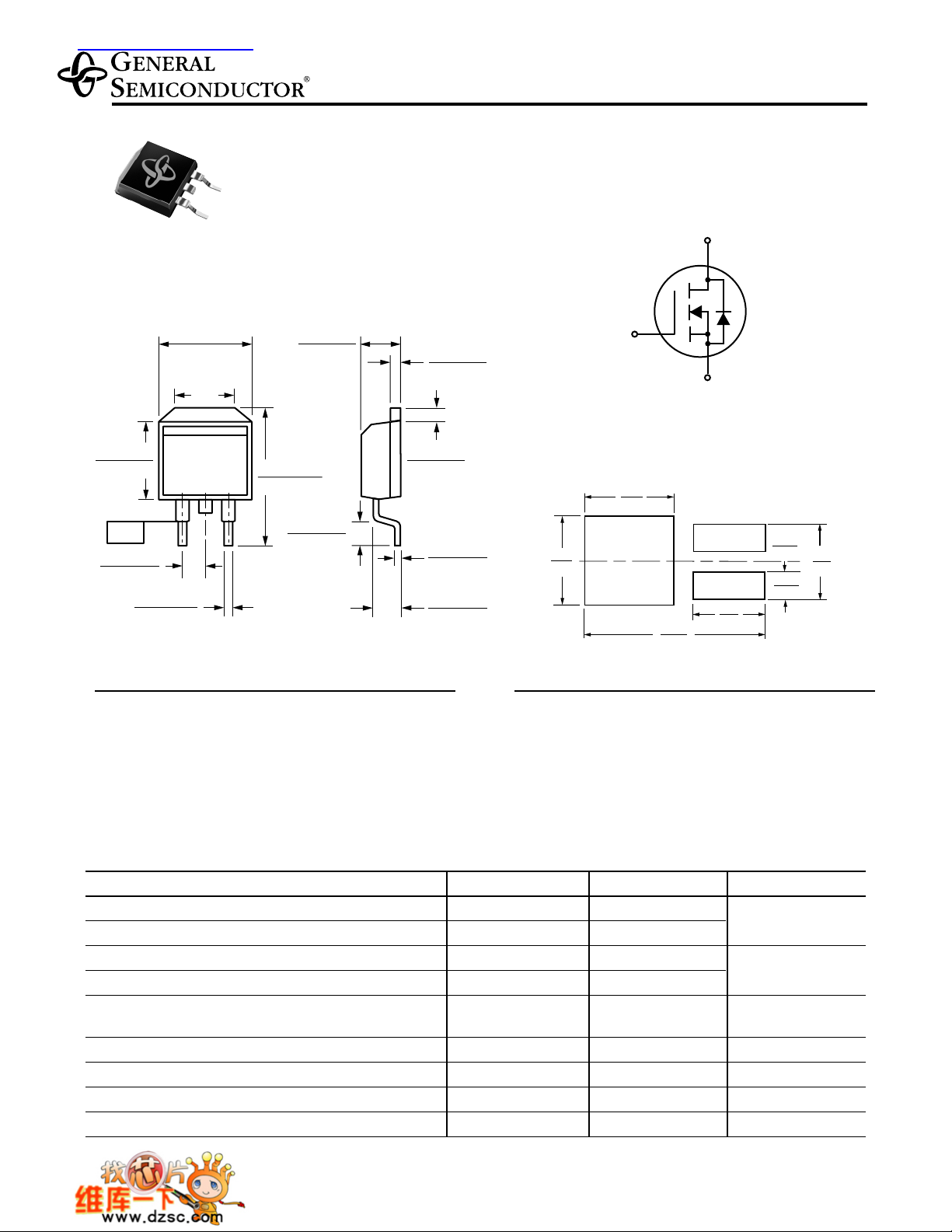
N-Channel Enhancement-Mode MOSFET
VDS30V R
DS(ON)
6.5mΩ ID75A
8/1/00
T
RENCH
G
EN
F
ET
TM
New Product
0.380 (9.65)
0.420 (10.67)
0.320 (8.13)
0.360 (9.14)
0.575 (14.60)
0.625 (15.88)
0.245 (6.22)
Min.
D
-T-
Seating Plate
0.027 (0.686)
0.037 (0.940)
0.095 (2.41)
0.100 (2.54)
GDS
PIN
0.160 (4.06)
0.190 (4.83)
0.045 (1.14)
0.055 (1.40)
0.090 (2.29)
0.110 (2.79)
0.047 (1.19)
0.055 (1.40)
0.018 (0.46)
0.025 (0.64)
0.080 (2.03)
0.110 (2.79)
Features
• Advanced Trench Process Technology
• High Density Cell Design for Ultra Low On-Resistance
• Specially Designed for Low Voltage DC/DC Converters
• Fast Switching for High Efficiency
• High temperature soldering in accordance with
CECC802/Reflow guaranteed
G
D
S
TO-263AB
Mechanical Data
Case: JEDEC TO-263 molded plastic body
Terminals: Leads solderable per MIL-STD-750,
Method 2026
Mounting Position: Any
Weight: 1.3g
Dimensions in inches and (millimeters)
0.08
(2.032)
0.04
(1.016)
0.24
(6.096)
0.42
(10.66)
0.63
(17.02)
0.12
(3.05)
0.33
(8.38)
Mounting Pad Layout
TO-263AB
查询GFB75N03供应商查询GFB75N03供应商
Electrical Characteristics(T
J
= 25°C unless otherwise noted)
Parameter Symbol Test Condition Min Typ Max Unit
Static
Drain-Source Breakdown Voltage BV
DSS
VGS= 0V, ID= 250µA30 ——V
Drain-Source On-State Resistance
(2)
R
DS(on)
VGS= 10V, ID= 38A — 5.8 6.5
mΩ
VGS= 4.5V, ID= 31A — 8.5 9.5
Gate Threshold Voltage V
GS(th)
VDS= VGS, ID= 250µA 1.0 — 3.0 V
Zero Gate Voltage Drain Current I
DSS
VDS= 30V, VGS= 0V ——1.0 µA
Gate-Body Leakage I
GSS
VGS= ±20V, VDS= 0V ——±100 nA
On-State Drain Current
(2)
I
D(on)
VDS≥ 5V, VGS= 10V 75 ——A
Forward Transconductance
(2)
g
fs
VDS= 15V, ID= 38A — 61 — S
Dynamic
Total Gate Charge Q
g
VDS=15V, ID=38A, VGS=5V — 32.5 46
— 63 90
Gate-Source Charge Q
gs
VDS= 15V, VGS= 10V
— 11 —
nC
Gate-Drain Charge Q
gd
ID= 38A
— 11 —
Turn-On Delay Time t
d(on)
— 13 26
Turn-On Rise Time t
r
VDD= 15V, RL= 15Ω
— 16 29
Turn-Off Delay Time t
d(off)
ID≅ 1A, V
GEN
= 10V
— 94 132
ns
Turn-Off Fall Time t
f
RG= 6Ω
— 38 57
Input Capacitance C
iss
— 3240 —
Output Capacitance C
oss
VDS= 15V, VGS= 0V
— 625 — pF
Reverse Transfer Capacitance C
rss
f = 1.0MH
Z
— 285 —
Source-Drain Diode
Max. Diode Forward Current I
S
———75 A
Diode Forward Voltage V
SD
IS= 38A, VGS= 0V — 0.9 1.3 V
Notes:
(1) Maximum DC current limited by
the package
(2) Pulse test; pulse width ≤ 300 µs,
duty cycle ≤ 2%
GFB75N03
N-Channel Enhancement-Mode MOSFET
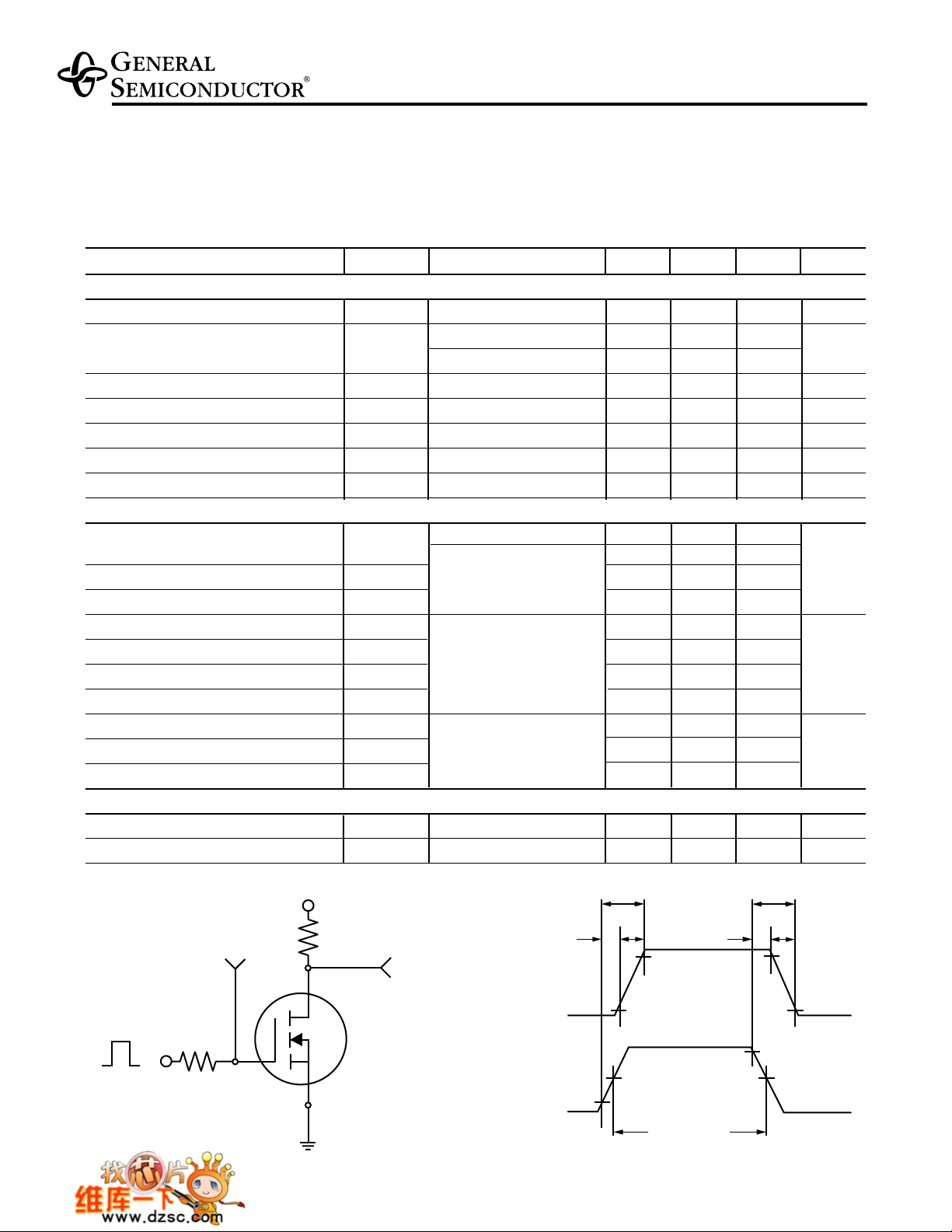
G
D
S
VIN
VDD
VGS
RGEN
RL
VOUT
DUT
Input, VIN
t
d(on)
Output, VOUT
t
on
t
r
t
d(off)
t
off
t
f
INVERTED
90%
10%10%
90 %
50%
50%
10%
90%
PULSE WIDTH
Switching T est Circuit Switching Waveforms

0
20
60
80
100
0123 4
Fig. 1 – Output Characteristics
0
0.002
0.004
0.006
0.008
0.01
0.012
0.014
0 20 40 60 80 100
Fig. 4 – On-Resistance vs.
Drain Current
0
10
20
40
30
50
70
60
12345
Fig. 2 – Transfer Characteristics
40
V
GS
= 2.5V
0.8
0.6
1.4
1.6
1.2
1
--50 --25 25 50 75 100 125 1500
Fig. 5 – On-Resistance vs.
Junction T emperature
VGS = 10V
I
D
= 38A
VGS = 4.5V
25°C
VGS = 10V
TJ = 125°C
--55°C
3.0V
3.5V
6.0V
4.0V
VDS = 10V
0
0.005
0.01
0.02
0.015
0.025
0.03
246810
Fig. 6 – On-Resistance vs.
Gate-to-Source V oltage
ID = 38A
TJ = 125°C
25°C
10V
0.5
1.3
1.1
1.5
1.7
0.7
0.9
--50 --25 25 50 75 100 125 1500
Fig. 3 – Threshold Voltage vs.
Temperature
ID = 250µA
I
D
-- Drain Source Current (A)
VDS -- Drain-to-Source Voltage (V)
R
DS(ON)
-- On-Resistance (Ω)
ID -- Drain Current (A)
I
D
-- Drain Source Current (A)
VGS -- Gate-to-Source Voltage (V)
R
DS(ON)
-- On-Resistance
(Normalized)
TJ -- Junction Temperature (°C)
V
(th)
-- Gate-to-Source Threshold Voltage (V)
TJ -- Junction Temperature (°C)
R
DS(ON)
-- On-Resistance (Ω)
VGS -- Gate-to-Source Voltage (V)
5.0V
80
0.016
4.5V
Ratings and
Characteristic Curves(T
A
= 25°C unless otherwise noted)
GFB75N03
N-Channel Enhancement-Mode MOSFET

36
35
37
39
40
38
--50 --25 25 50 75 100 1250
Fig. 10 – Breakdown Voltage vs.
Junction Temperature
150
ID = 250µA
0
500
1000
1500
2000
2500
3000
3500
4000
0 5 10 15
30
20 25
Fig. 8 – Capacitance
C
iss
C
rss
C
oss
f = 1MH
Z
VGS = 0V
0
2
4
6
8
10
01020 4030
Fig. 7 – Gate Charge
50 60 70
VDS = 15V
I
D
= 38A
0.01
0.1
1
10
100
0 0.2 0.4 0.6 0.8 1 1.2 1.4
TJ = 125°C
Fig. 9 – Source-Drain Diode
Forward V oltage
25°C --55°C
VGS = 0V
I
S
-- Source Current (A)
VSD -- Source-to-Drain Voltage (V)
BV
DSS
-- Breakdown Voltage (V)
TJ -- Junction Temperature (°C)
Q
g
-- Gate Charge (nC)
V
GS
-- Gate-to-Source Voltage (V)
C -- Capacitance (pF)
VDS -- Drain-to-Source Voltage (V)
41
Ratings and
Characteristic Curves(T
A
= 25°C unless otherwise noted)
GFB75N03
N-Channel Enhancement-Mode MOSFET
 Loading...