

Page 1
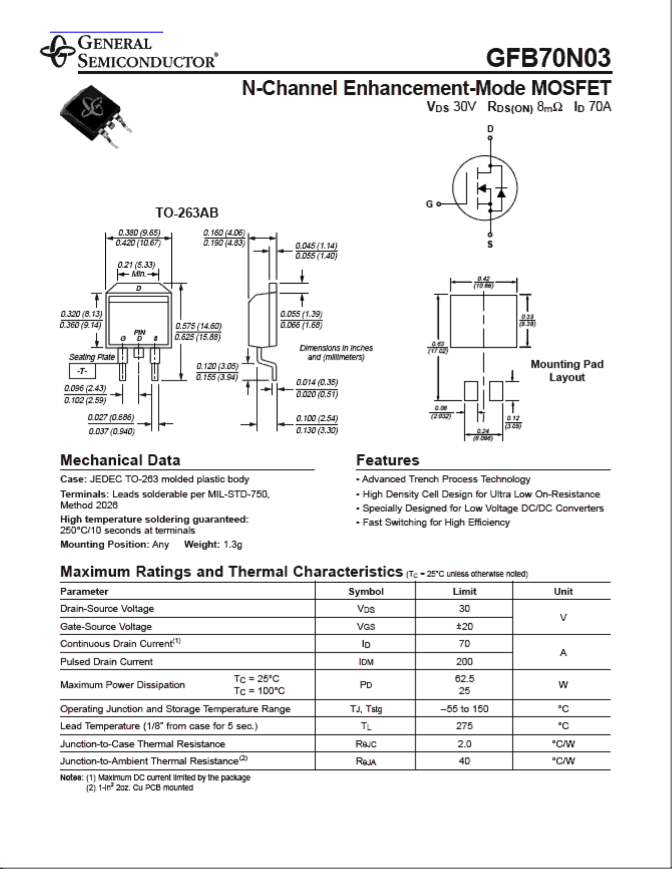
查询GFB70N03供应商
Page 2
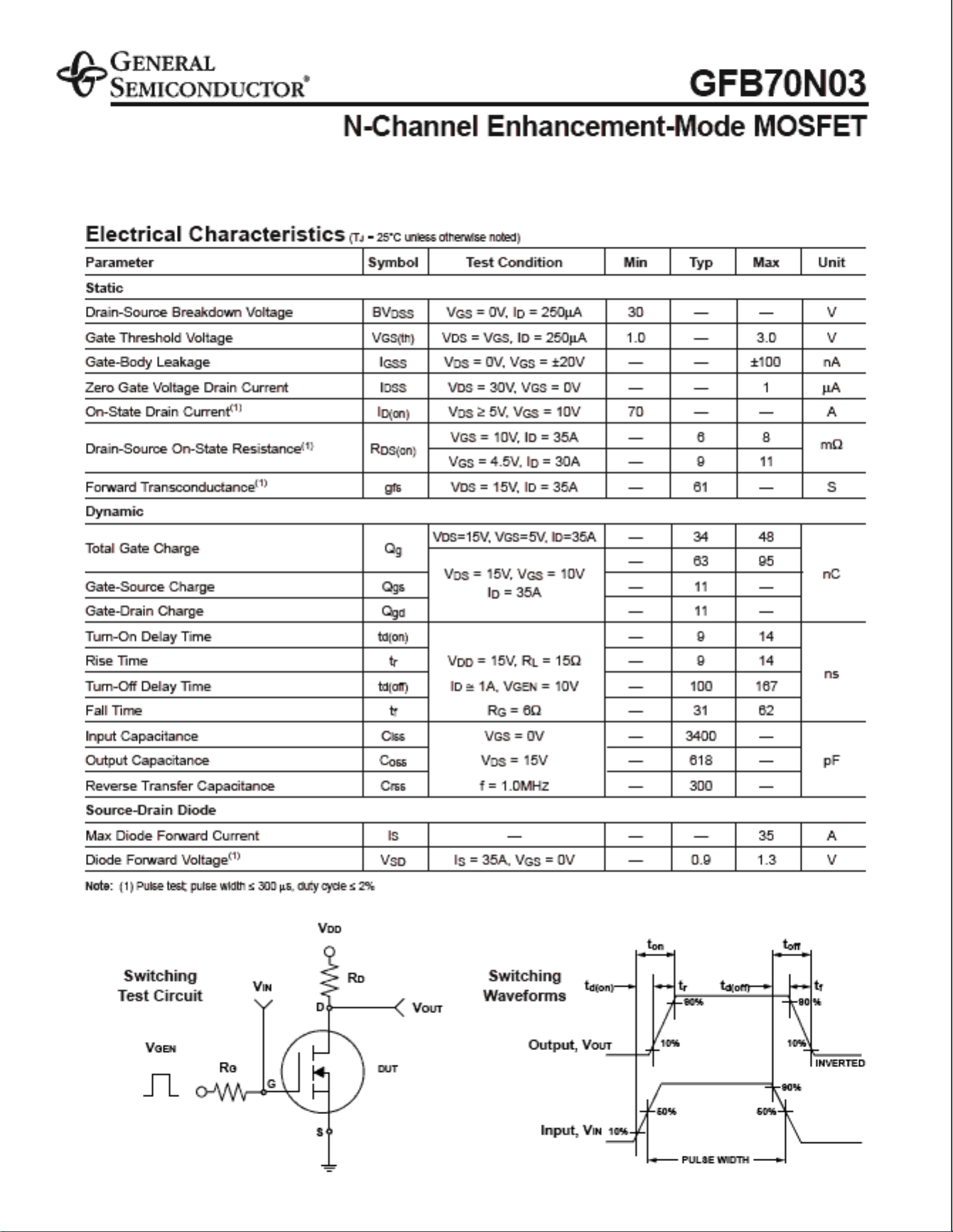
Page 3

0
10
20
30
50
60
70
0 0.5 1 1.5 2 2.5
Fig. 1 – Output Characteristics
0
0.002
0.004
0.006
0.008
0.01
0.012
0.014
0 20 40 60 80 100
Fig. 4 – On-Resistance vs.
Drain Current
0
10
20
40
30
50
70
60
12345
Fig. 2 – Transfer Characteristics
40
V
GS
= 2.5V
0.8
0.6
1.4
1.6
1.2
1
--50 --25 25 50 75 100 125 1500
Fig. 5 – On-Resistance vs.
Junction T emperature
VGS = 10V
I
D
= 35A
VGS = 4.5V
25°C
VGS = 10V
TJ = 125°C
--55°C
3.0V
3.5V
6.0V
4.0V
VDS = 10V
10V
0.6
1.4
1.2
1.6
1.8
0.8
1
--50 --25 25 50 75 100 125 1500
Fig. 3 – Threshold Voltage vs.
Temperature
ID = 250µA
I
D
-- Drain Source Current (A)
VDS -- Drain-to-Source Voltage (V)
R
DS(ON)
-- On-Resistance (Ω)
ID -- Drain Current (A)
I
D
-- Drain Current (A)
VGS -- Gate-to-Source Voltage (V)
R
DS(ON)
-- On-Resistance
(Normalized)
TJ -- Junction Temperature (°C)
V
GS(th)
-- Threshold Voltage (V)
TJ -- Junction Temperature (°C)
4.5V
Ratings and
Characteristic Curves(T
A
= 25°C unless otherwise noted)
GFB70N03
N-Channel Enhancement-Mode MOSFET
Page 4

0
500
1000
1500
2000
2500
3000
3500
4000
4500
0 5 10 15 3020 25
Fig. 8 – Capacitance
C
iss
C
rss
C
oss
f = 1MH
Z
VGS = 0V
0
2
4
6
8
10
01020 4030
Fig. 7 – Gate Charge
50 60 70
VDS = 15V
I
D
= 35A
0.01
0.1
1
10
100
0 0.2 0.4 0.6 0.8 1 1.2 1.4
TJ = 125°C
Fig. 9 – Source-Drain Diode
Forward V oltage
25°C --55°C
VGS = 0V
I
S
-- Source Current (A)
VSD -- Source-to-Drain Voltage (V)
Q
g
-- Gate Charge (nC)
V
GS
-- Gate-to-Source Voltage (V)
C -- Capacitance (pF)
VDS -- Drain-to-Source Voltage (V)
0
0.005
0.01
0.02
0.015
0.025
0.03
246810
Fig. 6 – On-Resistance vs.
Gate-to-Source V oltage
ID = 35A
TJ = 125°C
25°C
R
DS(ON)
-- On-Resistance (Ω)
VGS -- Gate-to-Source Voltage (V)
Ratings and
Characteristic Curves(T
A
= 25°C unless otherwise noted)
GFB70N03
N-Channel Enhancement-Mode MOSFET
Page 5

36
35
37
39
40
38
--50 --25 25 50 75 100 1250
Fig. 10 – Breakdown Voltage
vs. Junction Temperature
150
ID = 250µA
BV
DSS
-- Breakdown Voltage (V)
TJ -- Junction Temperature (°C)
Fig. 13 – Maxim um Saf e Operating Area
0.0001 0.001 0.01
0.01
0.1
0.1
1
1
10
I
D
-- Drain Current (A)
VDS -- Drain-Source Voltage (V)
Fig. 11 – Thermal Impedance
R
ΘJA (norm)
-- Normalized Thermal
Impedance
Pulse Duration (sec.)
Single Pulse
0.0010.0001 0.01 0.1
0
0.1
1
1
10
100
1000
10 100
200
400
600
800
1000
110
Fig. 12 – Power vs. Pulse Duration
Power (W)
Pulse Duration (sec.)
Single Pulse
R
θJC
= 2.0°C/W
T
C
= 25°C
VGS = 10V
Single Pulse
R
ΘJC
= 2.0 ¡C/W
T
C = 25°C
R
DS(ON)
Limit
100µs
1ms
10ms
DC
D = 0.5
0.2
0.1
t
1
t
2
P
DM
1. Duty Cycle, D = t1/t
2
2. R
θJC
(t) = R
θJC(norm)
*R
θJC
3. R
θJC
= 2.0°C/W
4. T
J
- TC = PDM * R
θJC
(t)
0.05
100ms
Ratings and
Characteristic Curves(T
A
= 25°C unless otherwise noted)
GFB70N03
N-Channel Enhancement-Mode MOSFET
 Loading...