

Maximum Ratings and Thermal Characteristics (T
A
= 25°C unless otherwise noted)
Parameter Symbol Limit Unit
Drain-Source Voltage V
DS
30 V
Gate-Source-Voltage V
GS
±
20 V
Continuous Drain Current TJ= 150°C TA= 25°C I
D
2.5 A
Pulsed Drain Current
(1)
I
DM
10 A
Maximum Power Dissipation
(2)
TA= 25°C 1.25
TA= 70°C
P
D
0.80
W
Operating Junction and Storage Temperature Range TJ, T
stg
–55 to +150 °C
Maximum Junction-to-Ambient Thermal Resistance
(2)
R
θJA
100 °C/W
Notes:
(1) Pulse width limited by maximum junction temperature.
(2) Surface mounted on FR4 board, (1” x 1”, 2oz. Cu)
GF2304
N-Channel Enhancement-Mode MOSFET
V
DS
30V R
DS(ON)
0.117Ω ID2.5A
5/3/01
Features
• Advanced trench process technology
• High density cell design for ultra-low on-resistance
• Popular SOT-23 package with copper lead-frame
for superior thermal and electrical capabilities
• Compact and low profile
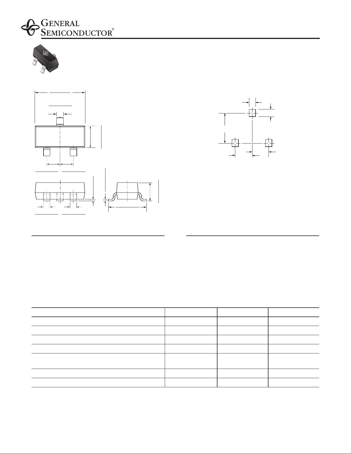
Mechanical Data
Case: SOT-23 Plastic Package
Weight: approx. 0.008g
Marking Code: 04
TO-236AB (SOT-23)
0.079 (2.0)
0.037 (0.95)
0.035 (0.9)
0.031 (0.8)
0.037 (0.95)
Mounting Pad Layout
T
RENCH
G
EN
F
ET
®
Pin Configuration
1. Gate
2. Source
3. Drain
max. .004 (0.1)
1
2
3
Top View
.020 (0.51)
.015 (0.37)
.118 (3.0)
.110 (2.8)
.055 (1.40)
.047 (1.20)
.098 (2.5)
.091 (2.3)
.041 (1.03)
.035 (0.89)
.041 (1.03)
.035 (0.89)
.007 (.180)
.003 (.085)
.020 (0.51)
.015 (0.37)
.020 (0.51)
.015 (0.37)
.047 (1.20)
.035 (0.90)
Dimensions in inches
and (millimeters)
GF2304
N-Channel Enhancement-Mode MOSFET
V
DS
30V R
DS(ON)
0.117Ω ID2.5A
Electrical Characteristics(T
J
= 25°C unless otherwise noted)
Parameter Symbol Test Condition Min Typ Max Unit
Static
Drain-Source Breakdown Voltage BV
DSS
VGS= 0V, ID= 250µA30 ––V
Gate Threshold Voltage V
GS(th)
VDS= VGS, ID= 250µA 1.0 –—V
Gate-Body Leakage I
GSS
VDS= 0V, VGS= ±20V ––±100 nA
Zero Gate Voltage Drain Current I
DSS
VDS= 30V, VGS= 0V ––0.5
µA
VDS=30V, VGS=0V , TJ=55°C ––10
On-State Drain Current
(1)
I
D(on)
VDS≥ 4.5V, VGS= 10V 6 ––
A
VDS≥ 4.5V, VGS= 4.5V 4 ––
Drain-Source On-State Resistance
(1)
R
DS(on)
VGS= 10V, ID= 2.5A – 0.096 0.117
Ω
VGS= 4.5V, ID= 2.0A – 0.135 0.190
Forward Transconductance
(1)
g
fs
VDS= 4.5V, ID= 2.5A – 4.6 – S
Dynamic
Total Gate Charge Q
g
– 3.7 10
Gate-Source Charge Q
gs
VDS= 15V, VGS= 10V
– 0.5 – nC
Gate-Drain Charge Q
gd
ID= 2.5A
– 0.6 –
Turn-On Delay Time t
d(on)
– 620
Rise Time t
r
VDD= 15V, RL= 15Ω
– 8.8 30
Turn-Off Delay Time t
d(off)
ID≈ 1A, V
GEN
= 10V
– 26 35
ns
Fall Time t
f
RG= 6Ω
– 2.4 20
Input Capacitance C
iss
VGS= 0V – 163 –
Output Capacitance C
oss
VDS= 15V – 27 – pF
Reverse Transfer Capacitance C
rss
f = 1.0MH
Z
– 9 –
Source-Drain Diode
Maximum Diode Forward Current I
S
———2.1 A
Diode Forward Voltage V
SD
IS = 1.25A, V
GS
= 0V – 0.82 1.2 V
Note: (1) Pulse test; pulse width ≤ 300 µs, duty cycle ≤ 2%
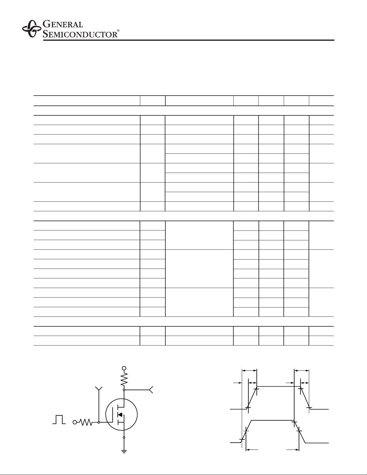
G
D
S
VIN
VDD
VGEN
RG
RD
VOUT
DUT
Input, VIN
t
d(on)
Output, VOUT
t
on
t
r
t
d(off)
t
off
t
f
INVERTED
90%
10%10%
90 %
50%
50%
10%
90%
PULSE WIDTH
Switching
Test Circuit
Switching
Waveforms

GF2304
N-Channel Enhancement-Mode MOSFET
0
2
4
6
10
0123 4 5
I
D
-- Drain-to-Source Current (A)
VDS -- Drain-to-Source Voltage (V)
0
0.06
0.12
0.18
02 4 6 8 10
Fig. 4 – On-Resistance
vs. Drain Current
R
DS(ON)
-- On-Resistance (Ω)
ID -- Drain Current (A)
0
012345
2
6
8
4
10
I
D
-- Drain Source Current (A)
VGS -- Gate-to-Source Voltage (V)
8
2
0
8
10
6
4
01 342
V
GS
-- Gate-to-Source Voltage (V)
Qg -- Gate Charge (nC)
Fig. 5 – Gate Charge
VDS = 15V
I
D
= 2.5A
10V
VDS = 10V
25°C
0
20
40
60
80
100
120
140
160
180
200
220
05 15 20 25 3010
C -- Capacitance (pF)
VDS Drain-to-Source Voltage (V)
Fig. 3 – Capacitance
f = 1 MHz
V
GS
= 0V
VGS = 5V, 6V, 7V, 8V, 10V
2.5V
4.5V
3.5V
3.0V
4.0V
--55°C
TJ = 125°C
C
oss
C
rss
C
iss
VGS = 4.5V
Ratings and
Characteristic Curves(T
A
= 25°C unless otherwise noted)

GF2304
N-Channel Enhancement-Mode MOSFET
Ratings and
Characteristic Curves(T
A
= 25°C unless otherwise noted)
1
10
0.3 0.5 0.7 0.9 1.1 1.3 1.5 1.7
TJ = 125°C
Fig. 7 – Source-Drain Diode
Forward V oltage
25°C
--55°C
VGS = 0V
I
S
-- Source Current (A)
VSD -- Source-to-Drain Voltage (V)
Fig. 6 – On-Resistance
vs. Gate-to-Source Voltage
0
0.1
0.2
0.4
0.3
2
R
DS(ON)
-- On-Resistance (Ω)
VGS -- Gate-to-Source Voltage (V)
46810
TJ = 125°C
25°C
35
37
39
41
43
45
--50 --25 25 50 75 100 1250
Fig. 8 – Breakdown Voltage vs.
Junction Temperature
150
ID = 250µA
BV
DSS
-- Breakdown Voltage (V)
TJ -- Junction Temperature (°C)
--50 --25 25 50 75 100 1250
0.6
0.8
1
1.2
1.4
1.6
Fig. 9 – Threshold V oltage
150
ID = 250µA
V
GS(th)
-- Gate-to-Source
Threshold Voltage (V)
TJ -- Junction Temperature (°C)
ID = 2.5A

GF2304
N-Channel Enhancement-Mode MOSFET
Ratings and
Characteristic Curves(T
A
= 25°C unless otherwise noted)
Fig. 13 – Maxim um Saf e Operating Area
0.0001 0.001 0.01
0.01
0.001
0.1
0.1
1
1
10 100
I
D
-- Drain Current (A)
VDS -- Drain-Source Voltage (V)
R
ΘJA (norm)
-- Normalized Thermal
Impedance
Pulse Duration (sec.)
0.6
0.8
1.0
1.2
1.4
1.6
1.8
--50 --25 25 50 75 100 1250
Fig. 10 – On-Resistance vs.
Junction T emperature
150
VGS = 10V
I
D
= 2.5A
R
DS(ON)
On-Resistance (Normalized)
TJ -- Junction Temperature (°C)
Single Pulse
0.001 0.01 0.1
0
0.01
0.1
0.1
1
1
10
100
10 100
5
10
15
20
1 10 100
Fig. 12 – Power vs. Pulse Duration
Power (W)
Pulse Duration (sec.)
Single Pulse
R
θJA
= 100°C/W
T
A
= 25°C
VGS = 10V
Single Pulse
R
θJA
= 100°C/W
T
A
= 25°C
R
DS(ON)
Limit
100µs
1ms
10ms
100ms
1s
DC
D = 0.5
0.2
0.01
0.1
t
1
t
2
P
DM
1. Duty Cycle, D = t1/t
2
2. R
θJA
(t) = R
θJA(norm)
*R
θJA
3. R
θJA
= 100°C/W
4. T
J
- TA = PDM * R
θJA
(t)
0.05
0.02
Fig. 11 – Thermal Impedance

 Loading...