BS850
DMOS Transistors (P-Channel)
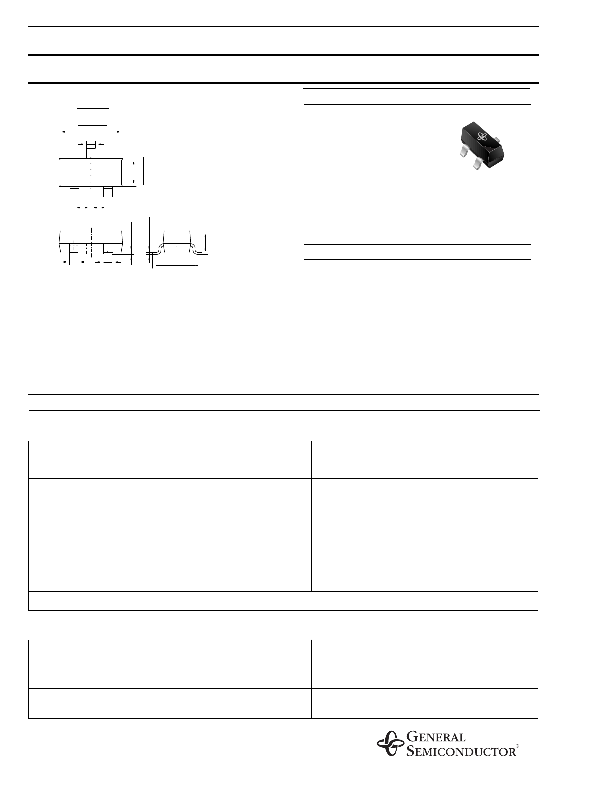
SOT-23
.122 (3.1)
.118 (3.0)
.016 (0.4)
3
12
.037(0.95).037(0.95)
.016 (0.4) .016 (0.4)
Dimensions in inches and (millimeters)
Pin configuration
1 = Gate, 2 = Source, 3 = Drain
Top View
)
.056 (1.43
max. .004 (0.1)
)
.052 (1.33
.007 (0.175)
.005 (0.125)
.102 (2.6)
.094 (2.4)
.045 (1.15)
FEATURES
High input i mpe dance
♦
High-speed sw itchi ng
♦
No minority carrier storage time
♦
CMOS logic com pat ible input
♦
No thermal runaway
♦
No secondary break down
♦
.037 (0.95)
SOT-23 Plastic Package
Case:
Weight:
Marking
S50
MECHANICAL DATA
approx. 0.008 g
Ratings at
Drain-Source Voltage –V
Drain-Gate Voltage –V
Gate-Source Voltage (pulsed) V
Drain Current (continuous) –I
Po w er Dissi pation at T
Junction Temperature T
Storage Temperature Range T
1)
Devic e on fiberglass substr ate, see layout
Invers e Diode
Max. Forw a rd Current (cont inuous )
at T
ambient temperature unless otherwise specified
25 °C
= 50 °C P
SB
= 25 °C
amb
MAXIMUM RATINGS AND ELECTRICAL CHARACTERISTICS
Symbol Value Unit
DSS
DGS
GS
D
tot
j
S
60 V
60 V
± 20 V
250 mA
1)
0.310
W
150 °C
–65 t o +150 °C
Symbol Value Unit
I
F
0.3 A
Forward V oltage Drop (typ.)
= 0, IF = 0.12 A, Tj = 25 °C
at V
GS
4/98
V
F
0.85 V

Ratings at
ambient temperature unless otherwise specified
25 °C
BS850
ELECTRICAL CHARACTERISTICS
Symbol Min. Typ. Max. Unit
Drain-Source Breakdo wn Voltage
at –I
D
= 100 µA, V
GS
= 0
Gate Threshold Voltage
= VDS, –ID = 1 mA
at V
GS
Gate-Body Leakage Current
at –V
Drain Cutoff Curr ent at –V
= 15 V, VDS = 0
GS
= 25 V, VGS = 0 –I
DS
Drain-Source ON Resis tance
at –V
= 10 V, –ID = 200 mA
GS
Thermal Resistance Junction t o Substrat e
Backside
Thermal Resistance Junction t o Ambient Air R
Forw ard Transconductance
at –V
= 10 V, –ID = 200 mA, f = 1 MHz
DS
Input Capacit ance
at –V
= 10 V, VGS = 0, f = 1 MHz
DS
Switching Times
at –V
= 10 V, –VDS = 10 V, RD = 100
GS
Ω
Turn-On Time
Turn-Off Time
1)
Device on fiberglas s substrat e, see la y out
–V
(BR)DSS
V
GS(th)
–I
GSS
DSS
R
DS(ON)
R
thSB
thJA
g
m
C
iss
t
on
t
off
60 90 – V
1.0 2 3.0 V
––10nA
––0.5µA
–3.55.0
– – 320
– – 450
1)
1)
Ω
K/W
K/W
– 200 – mS
–60–pF
–
–
5
25
–
–
ns
ns
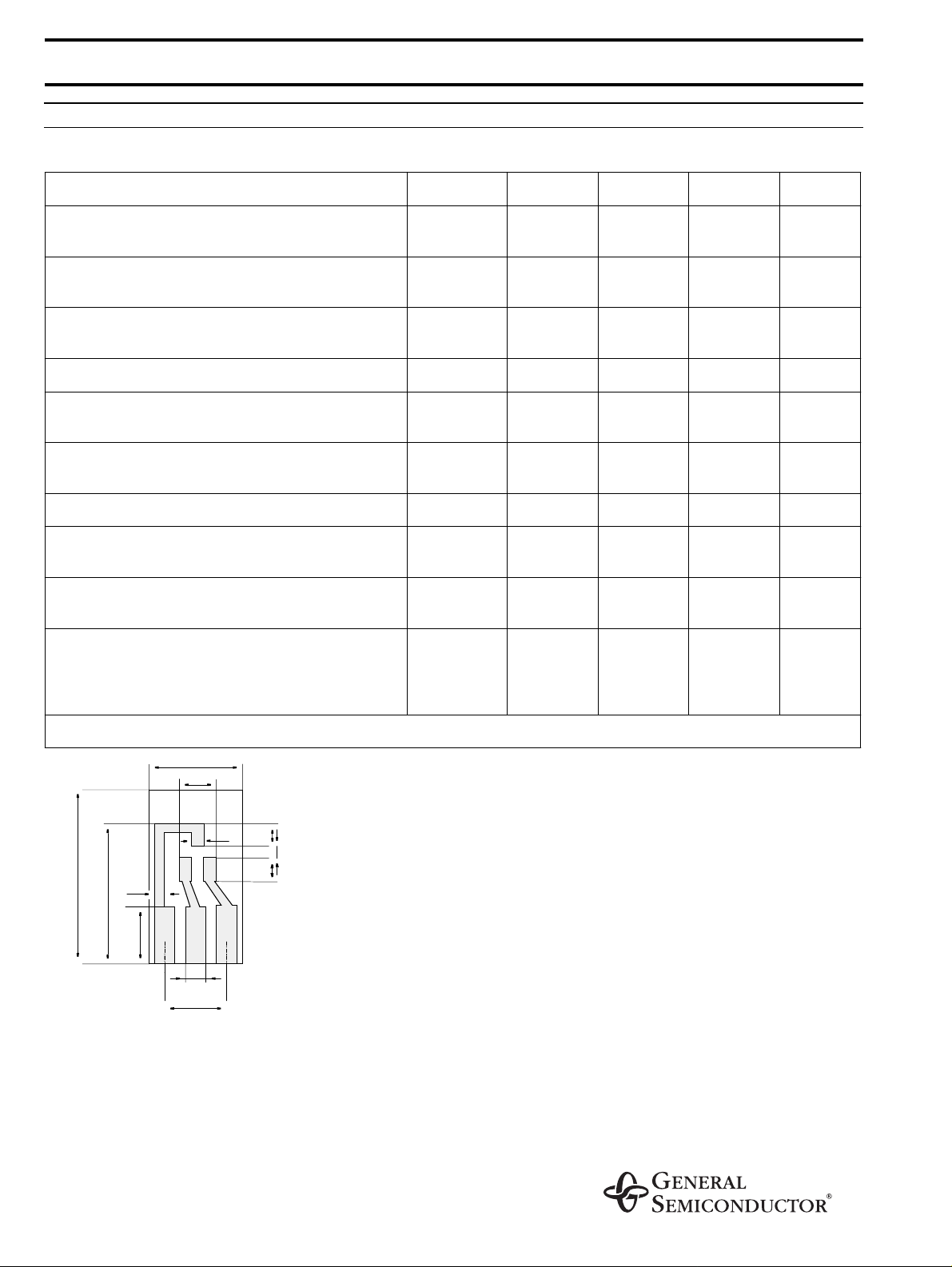
.30 (7.5)
.12 (3)
.04 ( 1)
.08 (2)
.04 (1)
.59 (15)
.03 (0.8)
.47 (12 )
0.2 (5)
Layou t f or R
thJA
.06 (1.5)
.20 (5.1)
test
.08 (2)
Dimensions in inches (millimeters)
Thickness: Fiberglass 0.059 in (1.5 mm)
Copper leads 0.012 in (0.3 mm)

RATINGS AND CHARACTERISTIC CURVES BS850

RATINGS AND CHARACTERISTIC CURVES BS850

RATINGS AND CHARACTERISTIC CURVES BS850
 Loading...