查询2N4126供应商
2N4126
Small Signal Transistors (PNP)
Ratings at
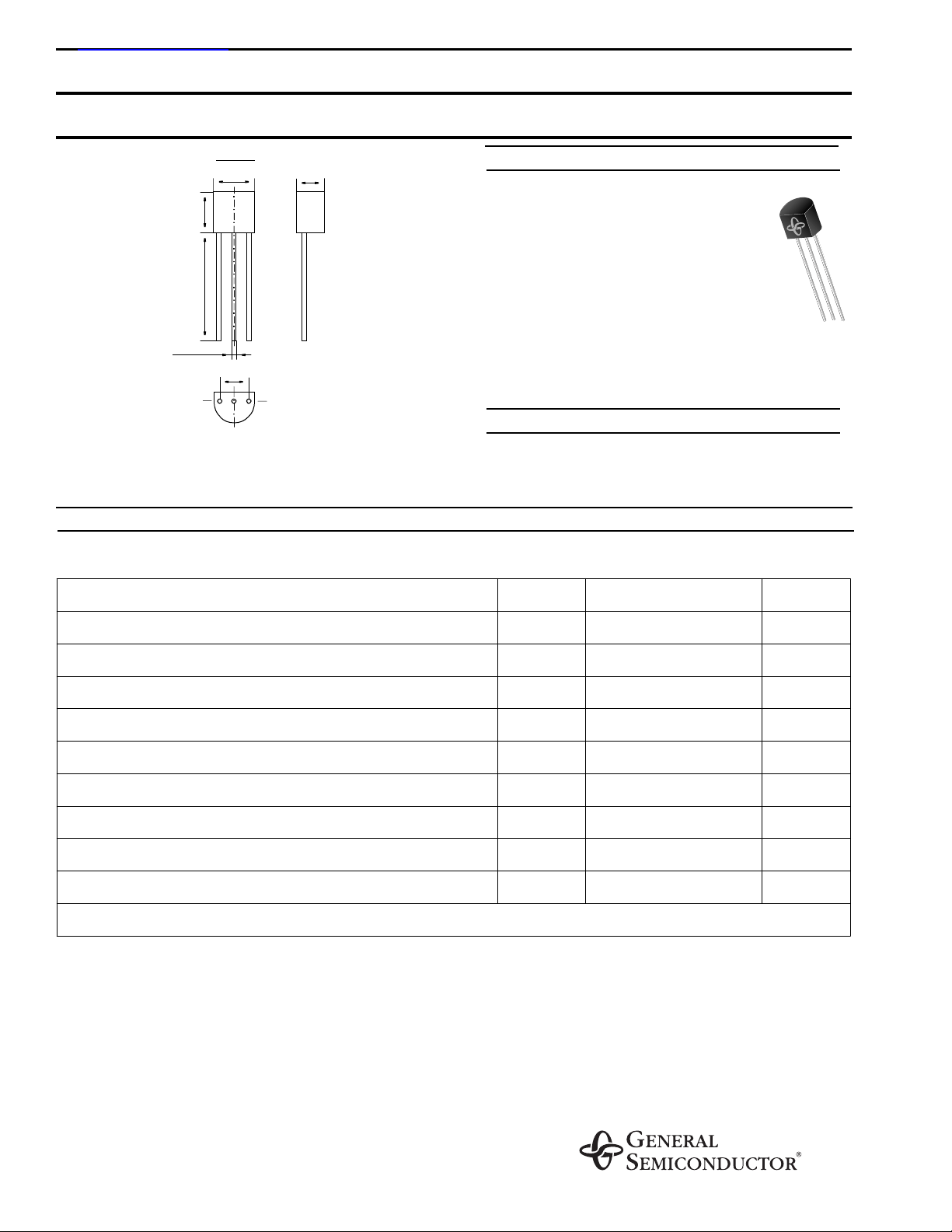
TO-92
.181 (4.6)
.181 (4.6)
min. .492 (12.5)
∅
.022 (0.55)
max.
.098 (2.5)
E
B
Dimensions in inches and (millimeters)
.142 (3.6)
C
MAXIMUM RATINGS AND ELECTRICAL CHARACTERISTICS
ambient temperature unless otherwise specified
25 °C
FEATURES
♦
PNP Silicon Epitaxial Transistor
for switching and amplifier applications.
Especially suit-able for AF-driver and
low-power output stages.
As complementary type, the NPN tran-
♦
sistor 2N4124 is recommended.
MECHANICAL DATA
TO-92 Plasti c Package
Case:
Weight:
approx. 0.18 g
Symbol Value Unit
Collector-Emitter Voltage –V
Collector-Base Voltage –V
Emitter-Base Voltage –V
Collector Current –I
Peak Collector Current –I
Base Current –I
Power Dissipation at T
= 25 °C P
amb
Junction Temperature T
Storage Temperature Range T
1)
Valid provided that leads are kept at ambient temperature at a distance of 2 mm from case.
CEO
CBO
EBO
C
CM
B
tot
j
S
25 V
25 V
4V
200 mA
800 mA
50 mA
1)
625
150 °C
–65 to +150 °C
mW
4/98

Ratings at
ambient temperature unless otherwise specified
25 °C
DC Current Gain
= –1 V, IC = –2.0 mA
at V
CE
at V
= –1 V, IC = –50 mA
CE
2N4126
ELECTRICAL CHARACTERISTICS
Symbol Min. Typ. Max. Unit
h
FE
h
FE
120
–
–
60
360
–
–
–
Collector Cutoff Current
= –20 V
at V
CB
Emitter Cutoff Current
= –3 V
at V
EB
Collector Saturation Voltage
= –50 mA, IB = –5 mA
at I
C
Base Saturation V oltage
= –50 mA, IB = –5 mA
at I
C
Collector-Emitter Breakdown Voltage
= –1 mA
at I
C
Collector-Base Brea kdown Volt age
= –10 µA
at I
C
Emitter-Base Breakdown Voltage
= –10 µA
at I
E
Gain-Bandwidth Product
= –5 V, IC = –10 mA, f = 50 MHz
at V
CE
Collector-Base Capac itance
= –10 V, f = 1 MHz
at V
CB
Thermal Resistance Junction to Ambient Air R
1)
Valid provided that leads are kept at ambient temperature at a distance of 2 mm from case.
–I
CBO
–I
EBO
–V
–V
–V
(BR) CEO
–V
(BR) CB O
–V
(BR)EB O
f
T
C
CBO
thJA
CESAT
BESAT
––50nA
––50nA
––0.4V
––0.95V
25––V
25––V
4––V
– 200 – MHz
–12– pF
– – 200
1)
K/W

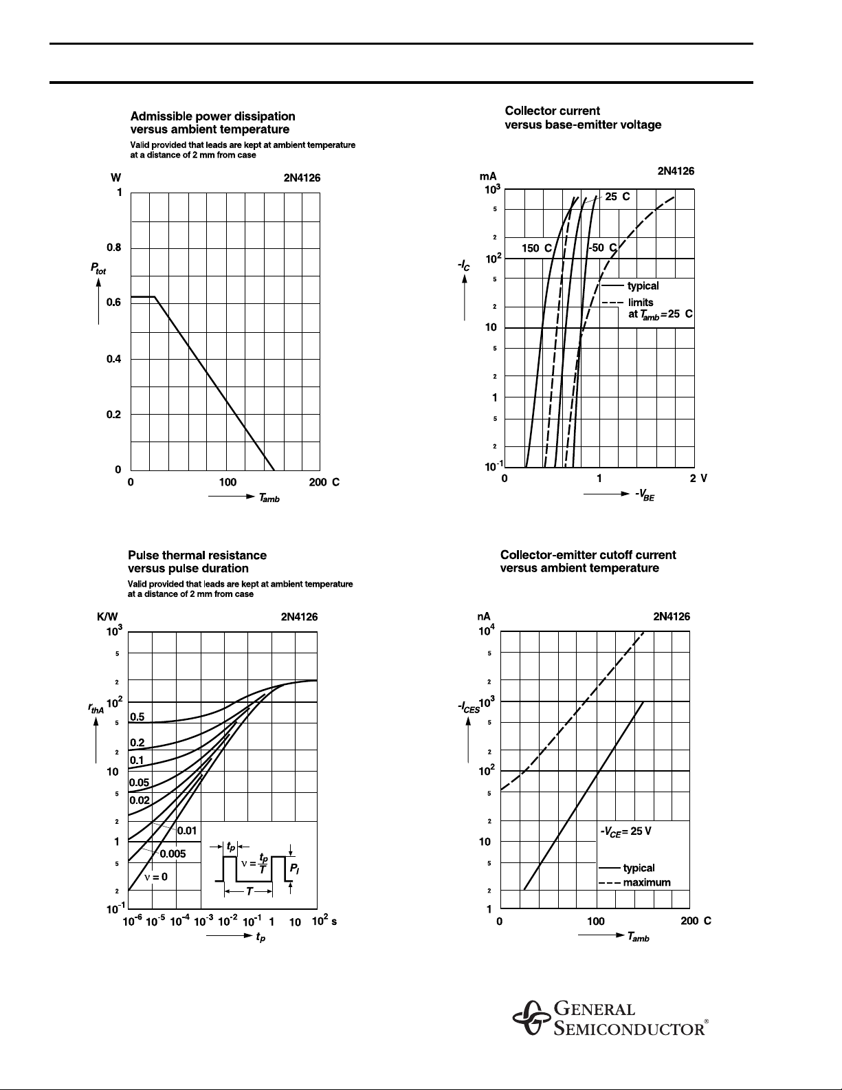
RATINGS AND CHARACTERISTIC CURVES 2N4126

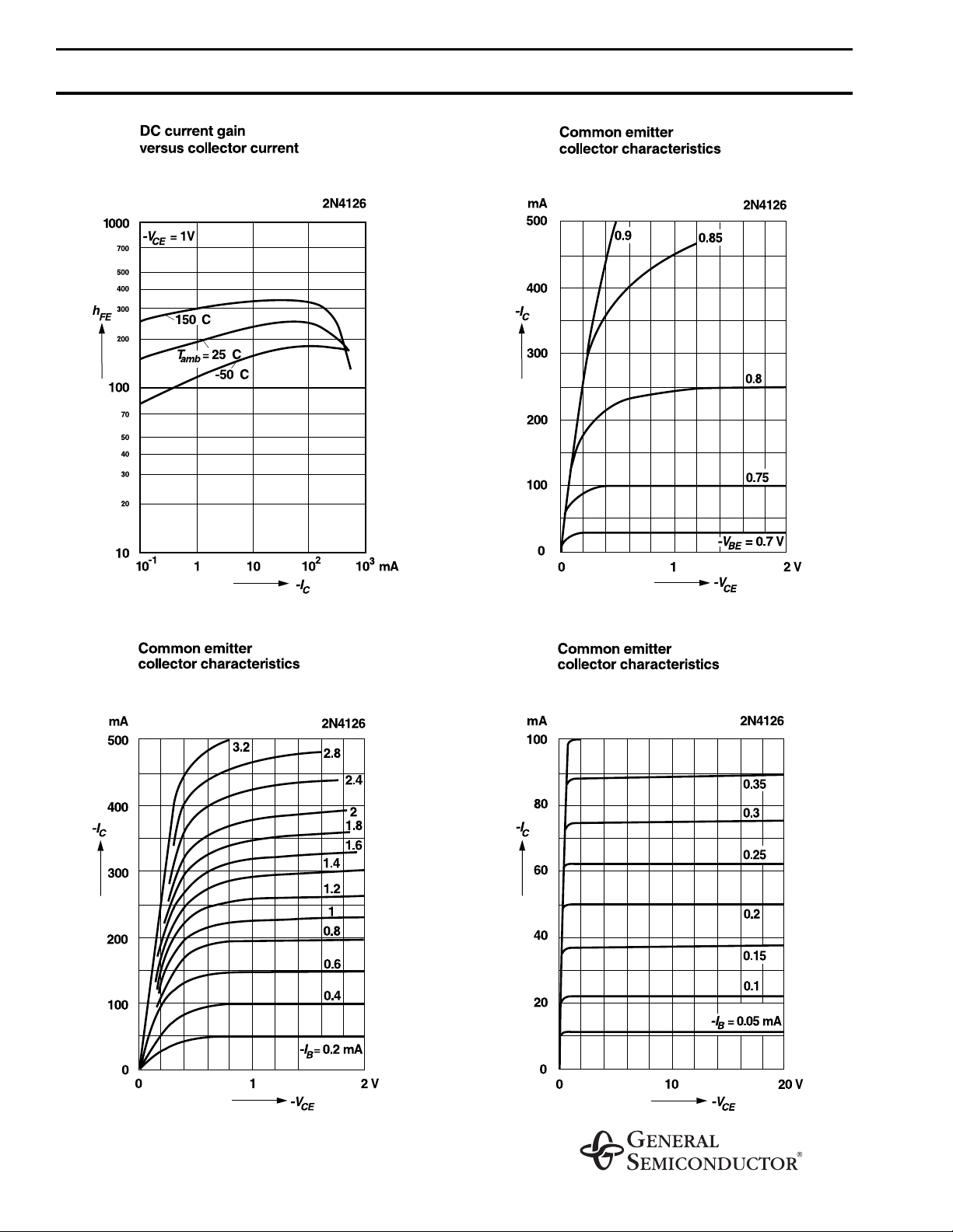
RATINGS AND CHARACTERISTIC CURVES 2N4126

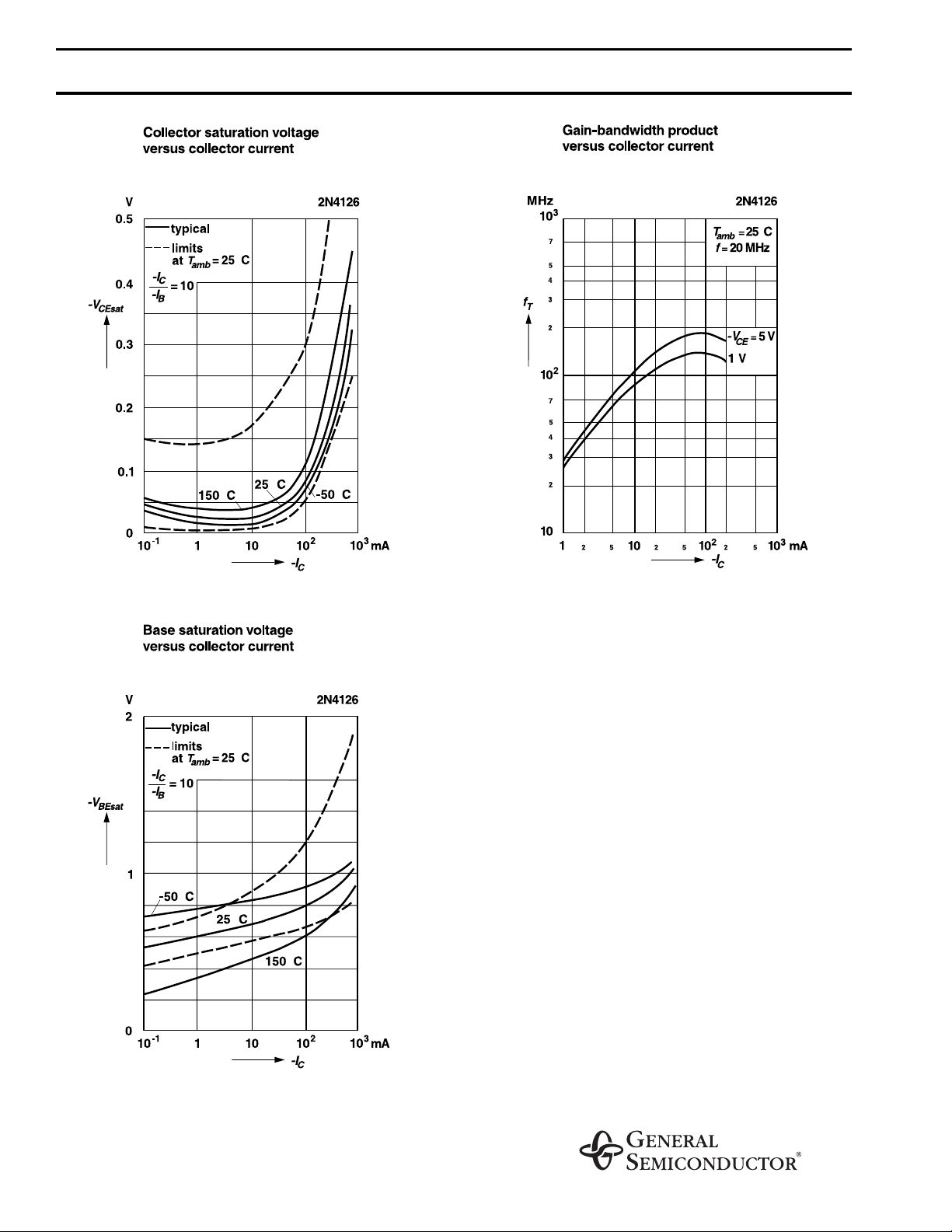
RATINGS AND CHARACTERISTIC CURVES 2N4126
 Loading...