

XT55 Hardware Interface Description
Confidential / Preliminary
s
mo b i l e
XT55
Siemens Cellular Engine
Version: 00.02
DocID: XT55_hd_v00.02
XT55_hd_v00.02 Page 1 of 116 15.03.2004

XT55 Hardware Interface Description
Confidential / Preliminary
s
mo b i l e
Document Name:
Version:
Date:
DocId:
Status:
XT55 Hardware Interface Description
00.02
March 15, 2004
XT55_hd_v00.02
Confidential / Preliminary
General note
Product is deemed accepted by Recipient and is provided without interface to Recipient´s products.
The Product constitutes pre-release version and code and may be changed substantially before
commercial release. The Product is provided on an “as is” basis only and may contain deficiencies or
inadequacies. The Product is provided without warranty of any kind, express or implied. To the
maximum extent permitted by applicable law, Siemens further disclaims all warranties, including
without limitation any implied warranties of merchantability, fitness for a particular purpose and
noninfringement of third-party rights. The entire risk arising out of the use or performance of the
Product and documentation remains with Recipient. This Product is not intended for use in life support
appliances, devices or systems where a malfunction of the product can reasonably be expected to
result in personal injury. Applications incorporating the described product must be designed to be in
accordance with the technical specifications provided in these guidelines. Failure to comply with any of
the required procedures can result in malfunctions or serious discrepancies in results. Furthermore, all
safety instructions regarding the use of mobile technical systems, including GSM products, which also
apply to cellular phones must be followed. Siemens AG customers using or selling this product for use
in any applications do so at their own risk and agree to fully indemnify Siemens for any damages
resulting from illegal use or resale. To the maximum extent permitted by applicable law, in no event
shall Siemens or its suppliers be liable for any consequential, incidental, direct, indirect, punitive or
other damages whatsoever (including, without limitation, damages for loss of business profits,
business interruption, loss of business information or data, or other pecuniary loss) arising out the use
of or inability to use the Product, even if Siemens has been advised of the possibility of such damages.
Subject to change without notice at any time.
Copyright
Transmittal, reproduction, dissemination and/or editing of this document as well as utilization of its
contents and communication thereof to others without express authorization are prohibited. Offenders
will be held liable for payment of damages. All rights created by patent grant or registration of a utility
model or design patent are reserved.
Copyright © Siemens AG 2004
XT55_hd_v00.02 Page 2 of 116 15.03.2004

XT55 Hardware Interface Description
Confidential / Preliminary
Contents
0 Document history....................................................................................................... 8
1 Introduction ................................................................................................................ 9
1.1 Related documents ............................................................................................. 9
1.2 Terms and abbreviations....................................................................................10
1.3 Type approval ....................................................................................................14
1.4 Safety precautions .............................................................................................16
2 Product concept........................................................................................................18
2.1 XT55 key features at a glance ...........................................................................19
2.2 Circuit concept ...................................................................................................22
3 GSM/GPRS application interface .............................................................................25
3.1 GSM/GPRS operating modes ............................................................................25
3.2 Power supply .....................................................................................................27
3.2.1 Power supply pins on the board-to-board connector.............................27
3.2.2 Minimizing power losses.......................................................................28
3.2.3 Monitoring power supply.......................................................................28
3.3 Power up / down scenarios ................................................................................29
3.3.1 Turn on the GSM/GPRS part of XT55 ..................................................29
3.3.1.1 Turn on the GSM/GPRS part of XT55 using the ignition line
GSM_IGT (Power on)...........................................................30
3.3.1.2 Timing of the ignition process...............................................31
3.3.1.3 Turn on the GSM/GPRS part of XT55 using the
GSM_POWER signal ...........................................................32
3.3.1.4 Turn on the GSM/GPRS part of XT55 using the RTC (Alarm
mode) ...................................................................................32
3.3.2 Turn off the GSM/GPRS part of XT55 ..................................................34
3.3.2.1 Turn off GSM/GPRS part of the XT55 module using AT
command..............................................................................34
3.3.2.2 Maximum number of turn-on / turn-off cycles........................35
3.3.2.3 Emergency shutdown using GSM_EMERGOFF pin .............35
3.3.3 Automatic shutdown .............................................................................36
3.3.3.1 Temperature dependent shutdown .......................................36
3.3.3.2 Temperature control during emergency call..........................37
3.3.3.3 Undervoltage shutdown if battery NTC is present.................37
3.3.3.4 Undervoltage shutdown if no battery NTC is present............38
3.3.3.5 Overvoltage shutdown..........................................................38
3.4 Automatic GPRS Multislot Class change............................................................39
3.5 GSM charging control ........................................................................................40
3.5.1 Battery pack characteristics..................................................................42
3.5.2 Recommended battery pack specification ............................................43
3.5.3 Implemented charging technique..........................................................44
3.5.4 Operating modes during charging ........................................................45
3.5.5 Charger requirements ..........................................................................46
3.6 Power saving .....................................................................................................47
3.6.1 No power saving (AT+CFUN=1)...........................................................47
3.6.2 NON-CYCLIC SLEEP mode (AT+CFUN=0) .........................................47
3.6.3 CYCLIC SLEEP mode (AT+CFUN=5, 6, 7, 8) ......................................47
3.6.4 CYCLIC SLEEP mode AT+CFUN=9 ....................................................48
s
mo b i l e
XT55_hd_v00.02 Page 3 of 116 15.03.2004

XT55 Hardware Interface Description
Confidential / Preliminary
3.6.5 Timing of the GSM_CTS signal in CYCLIC SLEEP modes...................48
3.6.6 Wake up XT55 from SLEEP mode.......................................................50
3.7 Summary of state transitions (except SLEEP mode)..........................................52
3.8 RTC backup for GSM/GPRS part of XT55.........................................................53
3.9 Serial interfaces of the XT55 GSM/GPRS part...................................................54
3.9.1 Features supported on the first serial interface of GSM/GPRS part
(ASC0) .................................................................................................54
3.9.2 Features supported on the second serial interface of GSM/GPRS part
(ASC1) .................................................................................................55
3.9.3 ASC0 and ASC1 configuration .............................................................55
3.10 Audio interfaces .................................................................................................56
3.10.1 Microphone circuit ................................................................................57
3.10.2 Speech processing...............................................................................58
3.10.3 DAI timing.............................................................................................58
3.11 SIM interface......................................................................................................60
3.11.1 Requirements for using the GSM_CCIN pin.........................................61
3.11.2 Design considerations for SIM card holder ...........................................62
3.12 Control signals ...................................................................................................63
3.12.1 Inputs ...................................................................................................63
3.12.2 Outputs.................................................................................................64
3.12.2.1 Synchronization signal..........................................................64
3.12.2.2 Using the GSM_SYNC pin to control a status LED...............65
3.12.2.3 Behavior of the GSM_RING0 line (ASC0 interface only) ......66
s
mo b i l e
4 GPS application interface.........................................................................................68
4.1 Theory of operation............................................................................................68
4.2 Technical data....................................................................................................69
4.3 GPS operating modes........................................................................................70
4.3.1 Trickle Power mode..............................................................................71
4.3.2 Comparision of Trickle Power and Push-to Fix mode ...........................72
4.4 Power supply of the XT55 GPS part ..................................................................73
4.5 General purpose input/output.............................................................................73
4.6 Serial interfaces of the XT55 GPS part ..............................................................74
4.7 GPS control signals............................................................................................74
4.8 Receiver architecture .........................................................................................75
4.9 Operation procedure ..........................................................................................76
4.10 Start-up procedures ...........................................................................................77
4.10.1 Coldstart...............................................................................................77
4.10.2 Warmstart ............................................................................................77
4.10.3 Hotstart.................................................................................................77
5 GSM and GPS antenna interfaces............................................................................78
5.1 GSM antenna installation ...................................................................................78
5.1.1 GSM antenna connector.......................................................................78
5.1.2 GSM antenna pad ................................................................................80
5.2 Installing the GPS antenna ................................................................................80
5.3 Hirose antenna connector ..................................................................................81
6 Electrical, reliability and radio characteristics .......................................................85
6.1 Absolute maximum ratings.................................................................................85
6.2 Operating temperatures .....................................................................................85
6.3 Pin description ...................................................................................................86
6.4 Power supply ratings..........................................................................................92
6.5 Current consumption during GSM/GPRS transmit burst ....................................94
XT55_hd_v00.02 Page 4 of 116 15.03.2004

XT55 Hardware Interface Description
Confidential / Preliminary
6.6 Electrical characteristics of the voiceband part...................................................99
6.6.1 Setting audio parameters by AT commands.........................................99
6.6.2 Audio programming model .................................................................100
6.6.3 Characteristics of audio modes ..........................................................101
6.6.4 Voiceband receive path ......................................................................102
6.6.5 Voiceband transmit path.....................................................................103
6.7 Air interface of the XT55 GSM/GPRS part .......................................................104
6.8 Electrostatic discharge.....................................................................................105
6.9 Reliability characteristics ..................................................................................106
7 Mechanics................................................................................................................107
7.1 Mechanical dimensions of XT55 ......................................................................107
7.2 Mounting XT55 onto the application platform ...................................................109
7.3 Board-to-board connector ................................................................................111
8 Reference approval.................................................................................................113
8.1 Reference equipment for type approval ...........................................................113
8.2 Compliance with FCC Rules and Regulations ..................................................114
s
mo b i l e
9 List of parts and accessories.................................................................................115
XT55_hd_v00.02 Page 5 of 116 15.03.2004

XT55 Hardware Interface Description
Confidential / Preliminary
s
mo b i l e
Figures
Figure 1: Block diagram of serial interface concept..............................................................23
Figure 2: Block diagram of XT55 for SiRF Demo application................................................24
Figure 3: Block diagram of XT55 with AVL or TCP/IP application (optional).........................24
Figure 4: Power supply limits during transmit burst ..............................................................28
Figure 5: Power-on by ignition signal....................................................................................30
Figure 6: Timing of power-on process if GSM_VDDLP is not used ......................................31
Figure 7: Timing of power-on process if GSM_VDDLP is fed from external source..............31
Figure 8: Deactivating GSM engine by GSM_EMERGOFF signal........................................35
Figure 9: Schematic of approved charging transistor, trickle charging and ESD protection ..40
Figure 10: Battery pack circuit diagram ................................................................................42
Figure 11: Charging process................................................................................................44
Figure 12: Timing of CTS signal (example for a 2.12 s paging cycle)...................................49
Figure 13: Beginning of power saving if CFUN=5 or 7..........................................................49
Figure 14: RTC supply from capacitor..................................................................................53
Figure 15: RTC supply from rechargeable battery................................................................53
Figure 16: RTC supply from non-chargeable battery............................................................53
Figure 17: Audio block diagram............................................................................................56
Figure 18: Schematic of microphone inputs .........................................................................57
Figure 19: DAI timing on transmit path .................................................................................59
Figure 20: DAI timing on receive path ..................................................................................59
Figure 21: SIM card holder of DSB45 Support Box ..............................................................62
Figure 22: Pin numbers of Molex SIM card holder on DSB45 Support Box ..........................62
Figure 23: GSM_SYNC signal during transmit burst.............................................................64
Figure 24: LED Circuit (Example).........................................................................................65
Figure 25: Incoming voice call..............................................................................................66
Figure 26: Incoming data call ...............................................................................................66
Figure 27: URC transmission ...............................................................................................66
Figure 28: Theory of operation .............................................................................................68
Figure 29: Example for current in Trickle Power mode.........................................................71
Figure 30: Current comparison between Trickle Power and Push-to Fix mode ....................72
Figure 31: Example of LED circuit ........................................................................................75
Figure 32: Receiver architecture of the GPS receiver...........................................................75
Figure 33: U.FL-R-SMT connector .......................................................................................78
Figure 34: Antenna pad and GND plane ..............................................................................78
Figure 35: Never use antenna connector and antenna pad at the same time.......................79
Figure 36: Restricted area around antenna pad ...................................................................79
Figure 37: GPS antenna connector (U.FL-R-SMT connector) ..............................................80
Figure 38: Mechanical dimensions of U.FL-R-SMT connector..............................................81
Figure 39: U.FL-R-SMT connector with U.FL-LP-040 plug ...................................................82
Figure 40: U.FL-R-SMT connector with U.FL-LP-066 plug ...................................................82
Figure 41: Specifications of U.FL-LP-(V)-040(01) plug.........................................................83
Figure 42: Pin assignment (top view on XT55).....................................................................86
Figure 43: Typical current consumption vs. return loss in EGSM 900 network .....................94
Figure 44: Typical current consumption vs. return loss in GSM 1800 network......................95
Figure 45: Typical current consumption vs. return loss in GSM 1900 network......................95
Figure 46: Peak current consumption during transmit burst in EGSM 900 network ..............96
Figure 47: Peak current consumption during transmit burst in GSM 1800 network ..............96
Figure 48: Peak current consumption during transmit burst in GSM 1900 network ..............97
Figure 49: Typical current consumption vs. return loss.........................................................98
Figure 50: AT audio programming model ...........................................................................100
Figure 51: XT55 – top view ................................................................................................107
XT55_hd_v00.02 Page 6 of 116 15.03.2004

XT55 Hardware Interface Description
Confidential / Preliminary
Figure 52: XT55 bottom view..............................................................................................107
Figure 53: Mechanical dimensions of XT55........................................................................108
Figure 54: Mounting holes on XT55 ...................................................................................109
Figure 55: Recommended dowel........................................................................................110
Figure 56: Mechanical dimensions of Hirose DF12 connector............................................112
Figure 57: Reference equipment for approval ....................................................................113
s
mo b i l e
Tables
Table 1: XT55 key features ..................................................................................................19
Table 2: GSM/GPRS coding schemes and maximum net data rates over air interface ........21
Table 3: Overview of GSM/GPRS operating modes.............................................................25
Table 4: Power supply pins of board-to-board connector .....................................................27
Table 5: AT commands available in Alarm mode .................................................................32
Table 6: Temperature dependent behavior ..........................................................................37
Table 7: Bill of material for external charging circuit .............................................................41
Table 8: Specifications of recommended battery pack .........................................................43
Table 9: Comparison Charge-only and Charge mode ..........................................................45
Table 10: AT commands available in Charge-only mode......................................................46
Table 11: Wake-up events in NON-CYCLIC and CYCLIC SLEEP modes............................50
Table 12: State transitions of XT55 (except SLEEP mode) ..................................................52
Table 13: DCE-DTE wiring of 1st serial interface (GSM/GPRS part)....................................55
Table 14: DCE-DTE wiring of 2nd serial interface (GSM/GPRS part)...................................55
Table 15: Signals of the SIM interface (board-to-board connector) ......................................60
Table 16: Pin assignment of Molex SIM card holder on DSB45 Support Box .......................62
Table 17: Input control signals of the GSM/GPRS part of the XT55 module ........................63
Table 18: Coding of the status LED......................................................................................65
Table 19: ASC0 ring signal...................................................................................................67
Table 20: Return loss ...........................................................................................................78
Table 21: Product specifications of U.FL-R-SMT connector .................................................81
Table 22: Material and finish of U.FL-R-SMT connector and recommended plugs...............82
Table 23: Ordering information for Hirose U.FL Series.........................................................84
Table 24: Absolute maximum ratings (GSM/GPRS part)......................................................85
Table 25: Absolute maximum rating (GPS part) ...................................................................85
Table 26: Operating temperatures........................................................................................85
Table 27: Electrical description of application interface ........................................................87
Table 28: Power supply ratings (GSM/GPRS part)...............................................................92
Table 29: Power supply ratings (GPS part) ..........................................................................93
Table 30: Audio parameters adjustable by AT command .....................................................99
Table 31: Voiceband characteristics (typical) .....................................................................101
Table 32: Voiceband receive path ......................................................................................102
Table 33: Voiceband transmit path.....................................................................................103
Table 34: Air Interface........................................................................................................104
Table 35: Measured electrostatic values ............................................................................105
Table 36: Summary of reliability test conditions..................................................................106
Table 37: Ordering information DF12 series.......................................................................111
Table 38: Electrical and mechanical characteristics of the Hirose DF12C connector..........111
Table 39: List of parts and accessories ..............................................................................115
Table 40: Molex sales contacts (subject to change) ...........................................................116
Table 41: Hirose sales contacts (subject to change) ..........................................................116
XT55_hd_v00.02 Page 7 of 116 15.03.2004

XT55 Hardware Interface Description
Confidential / Preliminary
s
mo b i l e
0 Document history
Preceding document: "XT55 Hardware Interface Description" Version 00.01
New document: "XT55 Hardware Interface Description" Version 00.02
Chapter Page What is new
Throughout this
document
1.1 9 Updated list of related documents
1.2 10 Added GPS terms abbreviations
2.1 19 Inserted new key features regarding GPS
2.2 22f Improved Figure 1, added Figure 2 and Figure 3
3.5.2 43 Deleted vendor XWODA, battery pack can be obtained from various dealers
4.1 68 New chapter: Theory of operation
4.3f 70 Detailed description of GPS operating modes
· Maximum temperature has been changed from +65°C to +70°C.
· Pins have been clearly divided into GPS and GSM pins.
4.4 73 Added information regarding the power supply pins of the GPS part
4.5 73 New chapter: General purpose input/output
4.6 74 More information regarding the two serial interfaces of the GPS part
4.7 74 Added a complete list of GPS control signals
4.8 75 New chapter describing the functionality of the integrated GPS receiver
4.9 76 New chapter: Operation procedure
4.10 77ff Detailed description of the GPS start-up procedure, coldstart, warmstart and
hotstart
6.3 86 Renamed chapter and corrected pin assignment of B2B connector
XT55_hd_v00.02 Page 8 of 116 15.03.2004

XT55 Hardware Interface Description
Confidential / Preliminary
s
mo b i l e
1 Introduction
This document describes the hardware interface of the Siemens XT55 module that connects
to the cellular device application and the air interface. As XT55 is intended to integrate with a
wide range of application platforms, all functional components are described in great detail.
This guide therefore covers all information needed to design and set up cellular applications
incorporating the XT55 module. It aids rapid retrieval of interface specifications, electrical
and mechanical details and information on the requirements to be considered for integration
of further components.
Please note that this document refers to the GPS software version 2.2.0 and XT55 module
software version 00.02.
1.1 Related documents
[1] XT55 AT Command Set, Version 00.02
[2] XT55 GPS Command Specification, Version 02
[3] XT55 AVL Software Instructions User’s Guide
[4] XT55 GPS Startup User's Guide
[5] GPRS Startup User's Guide
[6] Remote-SAT User's Guide
[7] DSB45 Support Box - Evaluation Kit for Siemens Cellular Engines
[8] Application Note 07: Li-Ion Batteries in GSM Applications (in preparation)
[9] Application Note 16: Upgrading XT55 Firmware (in preparation)
[10] Application Note 14: Audio and Battery Parameter Download (in preparation)
[11] Application Note 02: Audio Interface Design (in preparation)
[12] Multiplexer User's Guide
[13] Multiplex Driver Developer’s Guide for Windows 2000 and Windows XP
[14] Multiplex Driver Installation Guide for Windows 2000 and Windows XP
[15] Application Note 24: Application Developer’s Guide
Prior to using the XT55 engines or upgrading to a new firmware release, be sure to carefully
read the latest product information.
To visit the Siemens Website you can use the following link:
http://www.siemens.com/wm
XT55_hd_v00.02 Page 9 of 116 15.03.2004
XT55 Hardware Interface Description
Confidential / Preliminary
s
mo b i l e
1.2 Terms and abbreviations
Abbreviation Description
AD Analog / Digital
ADC Analog-to-Digital Converter
AFC Automatic Frequency Control
AGC Automatic Gain Control
ANSI American National Standards Institute
ARFCN Absolute Radio Frequency Channel Number
ARP Antenna Reference Point
ASC0 / ASC1 Asynchronous Controller. Abbreviations used for first and second serial interface of
XT55
ASIC Application Specific Integrated Circuit
B Thermistor Constant
B2B Board-to-board connector
BER Bit Error Rate
BTS Base Transceiver Station
CB or CBM Cell Broadcast Message
CE Conformité Européene (European Conformity)
CHAP Challenge Handshake Authentication Protocol
CPU Central Processing Unit
CS Coding Scheme
CSD Circuit Switched Data
CTS Clear to Send
DAC Digital-to-Analog Converter
DAI Digital Audio Interface
dBW Decibel per Watt
dBm0 Digital level, 3.14dBm0 corresponds to full scale, see ITU G.711, A-law
DCE Data Communication Equipment (typically modems, e.g. Siemens GSM engine)
DCS 1800 Digital Cellular System, also referred to as PCN
DGPS Differential GPS
DOP Dilution of Precision
DRX Discontinuous Reception
DSB Development Support Box
DSP Digital Signal Processor
DSR Data Set Ready
DTE Data Terminal Equipment (typically computer, terminal, printer or, for example, GSM
application)
DTR Data Terminal Ready
XT55_hd_v00.02 Page 10 of 116 15.03.2004
XT55 Hardware Interface Description
Confidential / Preliminary
Abbreviation Description
DTX Discontinuous Transmission
EFR Enhanced Full Rate
EGSM Enhanced GSM
EMC Electromagnetic Compatibility
ESD Electrostatic Discharge
ETS European Telecommunication Standard
FCC Federal Communications Commission (U.S.)
FDMA Frequency Division Multiple Access
FR Full Rate
GGA GPS Fixed Data
GMSK Gaussian Minimum Shift Keying
GPRS General Packet Radio Service
GPS Global Positioning System
s
mo b i l e
GSM Global Standard for Mobile Communications
HiZ High Impedance
HR Half Rate
I/O Input/Output
IC Integrated Circuit
IF Intermediate Frequency
IMEI International Mobile Equipment Identity
ISO International Standards Organization
ITU International Telecommunications Union
kbps kbits per second
LED Light Emitting Diode
Li-Ion Lithium-Ion
LNA Low Noise Amplifier
Mbps Mbits per second
MMI Man Machine Interface
MO Mobile Originated
MS Mobile Station (GSM engine), also referred to as TE
MSISDN Mobile Station International ISDN number
MSK Minimum Shift Key
MT Mobile Terminated
NTC Negative Temperature Coefficient
NMEA National Maritime Electronics Association
OEM Original Equipment Manufacturer
PA Power Amplifier
XT55_hd_v00.02 Page 11 of 116 15.03.2004
XT55 Hardware Interface Description
s
Confidential / Preliminary
Abbreviation Description
PAP Password Authentication Protocol
PBCCH Packet Switched Broadcast Control Channel
PCB Printed Circuit Board
PCL Power Control Level
PCM Pulse Code Modulation
PCN Personal Communications Network, also referred to as DCS 1800
PCS Personal Communication System, also referred to as GSM 1900
PDU Protocol Data Unit
PLL Phase Locked Loop
PPP Point-to-point protocol
PRN Pseudo-Random Noise Number – The identity of GPS satellites
PSU Power Supply Unit
R&TTE Radio and Telecommunication Terminal Equipment
mo b i l e
RAM Random Access Memory
RF Radio Frequency
RMS Root Mean Square (value)
ROM Read-only Memory
RP Receive Protocol
RTC Real Time Clock
RTCM Radio Technical Commission for Maritime Services
Rx Receive Direction
SA Selective Availability
SAR Specific Absorption Rate
SELV Safety Extra Low Voltage
SIM Subscriber Identification Module
SMS Short Message Service
SRAM Static Random Access Memory
TA Terminal adapter (e.g. GSM engine)
TDMA Time Division Multiple Access
TE Terminal Equipment, also referred to as DTE
Tx Transmit Direction
UART Universal asynchronous receiver-transmitter
URC Unsolicited Result Code
USSD Unstructured Supplementary Service Data
VSWR Voltage Standing Wave Ratio
WAAS W ide Area Augmentation System
XT55_hd_v00.02 Page 12 of 116 15.03.2004

XT55 Hardware Interface Description
Confidential / Preliminary
Abbreviation Description
Phonebook abbreviations
FD SIM fixdialing phonebook
LD SIM last dialing phonebook (list of numbers most recently dialed)
MC Mobile Equipment list of unanswered MT calls (missed calls)
ME Mobile Equipment phonebook
ON Own numbers (MSISDNs) stored on SIM or ME
RC Mobile Equipment list of received calls
SM SIM phonebook
s
mo b i l e
XT55_hd_v00.02 Page 13 of 116 15.03.2004
XT55 Hardware Interface Description
Confidential / Preliminary
s
mo b i l e
1.3 Type approval
XT55 is designed to comply with the directives and standards listed below. Please
note that the product is still in a pre-release state and, therefore, type approval and
testing procedures have not yet been completed.
European directives
99/05/EC “Directive of the European Parliament and of the council of 9 March
1999 on radio equipment and telecommunications terminal
equipment and the mutual recognition of their conformity”, in short
referred to as R&TTE Directive 1999/5/EC
89/336/EC Directive on electromagnetic compatibility
73/23/EC Directive on electrical equipment designed for use within certain
voltage limits (Low Voltage Directive)
Standards of North American Type Approval
CFR Title 47 “Code of Federal Regulations, Part 15, Part 22 and Part 24
(Telecommunications, PCS)”; US Equipment Authorization FCC
UL 60 950 “Product Safety Certification” (Safety requirements)
NAPRD.03 “Overview of PCS Type certification review board
Mobile Equipment Type Certification and IMEI control”
PCS Type Certification Review board (PTCRB)
Standards of European Type Approval
3GPP TS 51.010-1 “Digital cellular telecommunications system (Phase 2); Mobile Station
(MS) conformance specification”.
ETSI EN 301 511 “V7.0.1
communications
(GSM); Harmonized standard for mobile stations in the GSM 900 and
DCS 1800 bands covering essential requirements under article 3.2 of
the R&TTE directive (1999/5/EC) (GSM 13.11 version 7.0.1 Release
1998)”
GCF-CC “Global
ETSI EN 301 489-1 “V1.1.1
communications
spectrum Matters (ERM); Electro Magnetic Compatibility (EMC) standard
Requirements”
ETSI EN 301 489-07 “V1.1.1 Electro Magnetic Compatibility and Radio spectrum Matters
(ERM); Electro Magnetic Compatibility (EMC) standard for radio
equipment and services; Part 7: Specific conditions for mobile and
portable radio and ancillary equipment of digital cellular radio telecommunications systems (GSM and DCS)”
EN 60 950 Safety of information technology equipment (2000)
(2000-12) Candidate Harmonized European Standard (Tele-
series) Global System for Mobile communications
Certification Forum - Certification Criteria” V3.12.0 (Sept 2003)
(2000-09) Candidate Harmonized European Standard (Tele-
series) Electro Magnetic Compatibility and Radio
for radio equipment and services; Part 1: Common Technical
XT55_hd_v00.02 Page 14 of 116 15.03.2004

XT55 Hardware Interface Description
Confidential / Preliminary
s
mo b i l e
Requirements of quality
IEC 60068 Environmental testing
DIN EN 60529 IP codes
Compliance with international rules and regulations
Manufacturers of mobile or fixed devices incorporating XT55 modules are advised to have
their completed product tested and approved for compliance with all applicable national and
international regulations. As a tri-band GSM/GPRS engine designed for use on any GSM
network in the world, XT55 is required to pass all approvals relevant to operation on the
European and North American markets. For the North American market this includes the
Rules and Regulations of the Federal Communications Commission (FCC) and PTCRB, for
the European market the R&TTE Directives and GCF Certification Criteria must be fully
satisfied.
The FCC Equipment Authorization granted to the XT55 Siemens reference application is
valid only for the equipment described in Chapter 8.
SAR requirements specific to handheld mobiles
Mobile phones, PDAs or other handheld transmitters and receivers incorporating a GSM
module must be in accordance with the guidelines for human exposure to radio frequency
energy. This requires the Specific Absorption Rate (SAR) of handheld XT55 based
applications to be evaluated and approved for compliance with national and/or international
regulations.
Since the SAR value varies significantly with the individual product design manufacturers are
advised to submit their product for approval if designed for handheld operation. For
European and US markets the relevant directives are mentioned below. It is the
responsibility of the manufacturer of the final product to verify whether or not further
standards, recommendations or directives are in force outside these areas.
Products intended for sale on US markets
ES 59005/ANSI C95.1 Considerations for evaluation of human exposure to Electromagnetic
Fields (EMFs) from Mobile Telecommunication Equipment (MTE) in
the frequency range 30MHz-6GHz
Products intended for sale on European markets
EN 50360 Product standard to demonstrate the compliance of mobile phones
with the basic restrictions related to human exposure to
electromagnetic fields (300 MHz - 3 GHz)
Note: Usage of XT55 in a handheld or portable application is not allowed without a
new FCC certification.
XT55_hd_v00.02 Page 15 of 116 15.03.2004
XT55 Hardware Interface Description
Confidential / Preliminary
s
mo b i l e
1.4 Safety precautions
The following safety precautions must be observed during all phases of the operation,
usage, service or repair of any cellular terminal or mobile incorporating XT55. Manufacturers
of the cellular terminal are advised to convey the following safety information to users and
operating personnel and to incorporate these guidelines into all manuals supplied with the
product. Failure to comply with these precautions violates safety standards of design,
manufacture and intended use of the product. Siemens AG assumes no liability for customer
failure to comply with these precautions.
When in a hospital or other health care facility, observe the restrictions on the
use of mobiles. Switch the cellular terminal or mobile off, if instructed to do so
by the guidelines posted in sensitive areas. Medical equipment may be
sensitive to RF energy.
The operation of cardiac pacemakers, other implanted medical equipment
and hearing aids can be affected by interference from cellular terminals or
mobiles placed close to the device. If in doubt about potential danger, contact
the physician or the manufacturer of the device to verify that the equipment is
properly shielded. Pacemaker patients are advised to keep their hand-held
mobile away from the pacemaker, while it is on.
Switch off the cellular terminal or mobile before boarding an aircraft. Make
sure it cannot be switched on inadvertently. The operation of wireless
appliances in an aircraft is forbidden to prevent interference with
communications systems. Failure to observe these instructions may lead to
the suspension or denial of cellular services to the offender, legal action, or
both.
Do not operate the cellular terminal or mobile in the presence of flammable
gases or fumes. Switch off the cellular terminal when you are near petrol
stations, fuel depots, chemical plants or where blasting operations are in
progress. Operation of any electrical equipment in potentially explosive
atmospheres can constitute a safety hazard.
Your cellular terminal or mobile receives and transmits radio frequency
energy while switched on. Remember that interference can occur if it is used
close to TV sets, radios, computers or inadequately shielded equipment.
Follow any special regulations and always switch off the cellular terminal or
mobile wherever forbidden, or when you suspect that it may cause
interference or danger.
Road safety comes first! Do not use a hand-held cellular terminal or mobile
when driving a vehicle, unless it is securely mounted in a holder for handsfree
operation. Before making a call with a hand-held terminal or mobile, park the
vehicle.
Handsfree devices must be installed by qualified personnel. Faulty installation
or operation can constitute a safety hazard.
XT55_hd_v00.02 Page 16 of 116 15.03.2004

XT55 Hardware Interface Description
Confidential / Preliminary
IMPORTANT!
SOS
Cellular terminals or mobiles operate using radio signals and cellular
networks. Because of this connection cannot be guaranteed at all times
under all conditions. Therefore, you should never rely solely upon any
wireless device for essential communications, for example emergency calls.
Remember, in order to make or receive calls, the cellular terminal or mobile
must be switched on and in a service area with adequate cellular signal
strength.
Some networks do not allow for emergency calls if certain network services
or phone features are in use (e.g. lock functions, fixed dialing etc.). You may
need to deactivate those features before you can make an emergency call.
Some networks require that a valid SIM card be properly inserted in the
cellular terminal or mobile.
s
mo b i l e
XT55_hd_v00.02 Page 17 of 116 15.03.2004

XT55 Hardware Interface Description
Confidential / Preliminary
s
mo b i l e
2 Product concept
Designed for use on any GSM network in the world, Siemens XT55 is a tri-band GSM/GPRS
engine that works on the three frequencies GSM 900 MHz, GSM 1800 MHz and GSM
1900 MHz and supports also GPS technology for satellite navigation. XT55 features GPRS
multislot class 10 and supports the GPRS coding schemes CS-1, CS-2, CS-3 and CS-4.
The compact design of the XT55 module makes it easy to integrate GSM / GPRS and GPS
as an all-in-one solution. It saves significantly both time and cost for integration of additional
hardware components.
The integrated GPS module provides instant location information using satellite signals to
enable users to ascertain where they are anywhere in the world. It consists of a fully
integrated RF receiver and a 12 channel baseband.
The tiny XT55 module incorporates all you need to create high-performance GSM/GPRS
solutions: baseband processor, power supply ASIC, complete radio frequency circuit
including a power amplifier and antenna interface. The power amplifier is directly fed from
the supply voltage GSM_BATT+. A compact “stacked FLASH / SRAM” device stores the
XT55 software in the flash memory section, and static RAM section provides the additional
storage capacity required by GPRS connectivity.
The physical interface to the cellular application is made through a board-to-board
connector. It consists of 80 pins, required for controlling the unit, receiving GPS location
data, transferring data and audio signals and providing power supply lines.
XT55 comprises two serial GSM interfaces (ASC0 and ASC1) and two serial GPS interfaces
(Serial data 1 and Serial data 2) giving you maximum flexibility for easy integration with the
Man-Machine Interface (MMI).
An extremely versatile audio concept offers various audio interfaces, each available on the
board-to-board connector: a digital audio interface (DAI) and two analog audio interfaces.
Using AT commands you can easily switch back and forth and select different audio modes.
The external dual-band or triple-band GSM/GPRS antenna can be connected optionally to a
connector on the top side or to a pad on the bottom side. A separate GPS antenna must be
connected to the GPS part of the module in order to properly receive satellite data.
For battery powered applications, XT55 features a charging control which can be used to
charge a Li-Ion battery. The charging circuit must be implemented outside the module on the
application platform.
XT55_hd_v00.02 Page 18 of 116 15.03.2004

XT55 Hardware Interface Description
Confidential / Preliminary
s
mo b i l e
2.1 XT55 key features at a glance
Table 1: XT55 key features
Feature Implementation
Power supply Supply voltage 3.3V – 4.8V for the GSM / GPRS module
Separate power supply source: 3.3V ± 5% for the GPS device
Power saving (GSM) Minimizes power consumption in SLEEP mode to 3mA
Power saving (GPS) TricklePower™ mode reduces power to < 60mW
Charging Supports charging control for Li-Ion battery for the GSM/GPRS part of the
module
Frequency bands
GSM class Small MS
Transmit power
GPRS connectivity
GPS features
Temperature range
Temperature control
and auto switch-off
DATA GPRS:
CSD:
WAP:
· Tri-band: EGSM 900, GSM 1800, GSM 1900
· Compliant to GSM Phase 2/2+
· Class 4 (2W) at EGSM900
· Class 1 (1W) at GSM1800 and GSM 1900
· GPRS multi-slot class 10
· GPRS mobile station class B
· GPS receiver with SiRFstar Ile/LP chip set
· Processor type ARM7/TDMI
· Sirf GSW2, version 2.2.0
· Normal operation: -20°C to +55°C
· Restricted operation: -25°C to -20°C and +55°C to +70°C
· Constant temperature control prevents damage to XT55 when the
specified temperature is exceeded. When an emergency call is in
progress the automatic temperature shutdown functionality is
deactivated.
· GPRS data downlink transfer: max. 85.6 kbps (see Table 2)
· GPRS data uplink transfer: max. 42.8 kbps (see Table 2
· Coding scheme: CS-1, CS-2, CS-3 and CS-4
· XT55 supports the two protocols PAP (Password Authentication
Protocol) and CHAP (Challenge Handshake Authentication Protocol)
commonly used for PPP connections.
· Support of Packet Switched Broadcast Control Channel (PBCCH) allows
you to benefit from enhanced GPRS performance when offered by the
network operators.
· CSD transmission rates: 2.4, 4.8, 9.6, 14.4 kbps, non-transparent, V.110
· Unstructured Supplementary Services Data (USSD) support
· WAP compliant
SMS
MMS MMS compliant
XT55_hd_v00.02 Page 19 of 116 15.03.2004
· MT, MO, CB, Text and PDU mode
· SMS storage: SIM card plus 25 SMS locations in the mobile equipment
· Transmission of SMS alternatively over CSD or GPRS. Preferred mode
can be user-defined.

XT55 Hardware Interface Description
Confidential / Preliminary
Feature Implementation
FAX Group 3: Class 1, Class 2
SIM interface
Supported SIM card: 3V
External SIM card reader has to be connected via interface connector (note
that card reader is not part of XT55)
s
mo b i l e
External antenna
GSM / GPRS:
GPS:
Audio interfaces Two analog audio interfaces, one digital audio interface (DAI)
Audio features Speech codec modes:
Two serial GSM
interfaces:
ASC0, ASC1
Connected via 50 Ohm antenna connector or antenna pad
Separate GPS antenna connector, see Figure 51 for details
· Half Rate (ETS 06.20)
· Full Rate (ETS 06.10)
· Enhanced Full Rate (ETS 06.50 / 06.60 / 06.80)
· Adaptive Multi Rate (AMR)
Handsfree operation
· Echo cancellation
· Noise reduction
· 2.65V level, bi-directional bus for AT commands and data
· ASC0 – full-featured 8-wire serial interface. Supports RTS0/CTS0
hardware handshake and software XON/XOFF flow control. Multiplex
ability according to GSM 07.10 Multiplexer Protocol.
· ASC1 - 4-wire serial interface. Supports RTS1/CTS1 hardware
handshake and software XON/XOFF flow control.
· Baud rate: 300bps ... 230kbps on ASC0 and ASC1
· Autobauding (on ASC0 only) detects 1200, 2400, 4800, 9600, 19200,
38400, 57600, 115200, 230400 bps
Two serial GPS
interfaces: SDn1, SDn2
Phonebook
management
SIM Application Toolkit Supports SAT class 3, GSM 11.14 Release 98
Ringing tones Offers a choice of 7 different ringing tones / melodies, easily selectable with
Real time clock Implemented
Timer function Programmable via AT command
Support of TTY/CTM To benefit from TTY communication via GSM, CTM equipment can be
Physical characteristics Size: 35.0 ± 0.15mm x 53.0 ± 0.15mm x 5.1 ± 0.15mm
Firmware upgrade XT55 firmware upgradable over serial interface
Evaluation kit The DSB45 Support Box is an evaluation kit designed to test and type
· Baud rate: 4800, 9600 bps on SD1 and SD2
Supported phonebook types: SM, FD, LD, MC, RC, ON, ME
AT command
connected to one of the three audio interfaces.
Weight: 11g
approve Siemens cellular engines and provide a sample configuration for
application engineering. See Chapter 9 for ordering information.
XT55_hd_v00.02 Page 20 of 116 15.03.2004

XT55 Hardware Interface Description
Confidential / Preliminary
Table 2: GSM/GPRS coding schemes and maximum net data rates over air interface
Coding scheme 1 Timeslot 2 Timeslots 4 Timeslots
CS-1: 9.05 kbps 18.1 kbps 36.2 kbps
CS-2: 13.4 kbps 26.8 kbps 53.6 kbps
CS-3: 15.6 kbps 31.2 kbps 62.4 kbps
CS-4: 21.4 kbps 42.8 kbps 85.6 kbps
Please note that the values stated above are maximum ratings which, in practice, are influenced by a
great variety of factors, primarily, for example, traffic variations and network coverage.
s
mo b i l e
XT55_hd_v00.02 Page 21 of 116 15.03.2004

XT55 Hardware Interface Description
Confidential / Preliminary
2.2 Circuit concept
The XT55 module comprises the following major functional components:
GSM / GPRS baseband block:
· Baseband controller operating at 26MHz
· Power supply ASIC
· Stacked Flash / SRAM
· Application interface (board-to-board connector)
GSM RF block:
· Skyworks RF transceiver
· Skyworks RF power amplifier / FEM
· RF front end (antenna connector)
GPS block:
· Processor Type ARM7/TDMI
· Processor speeds 6MHz, 12.5 MHz, 25 MHz, 49 MHz
GPS RF block:
· GPS receiver with SiRFstar Ile/LP chip set
s
mo b i l e
XT55_hd_v00.02 Page 22 of 116 15.03.2004
XT55 Hardware Interface Description
Confidential / Preliminary
s
mo b i l e
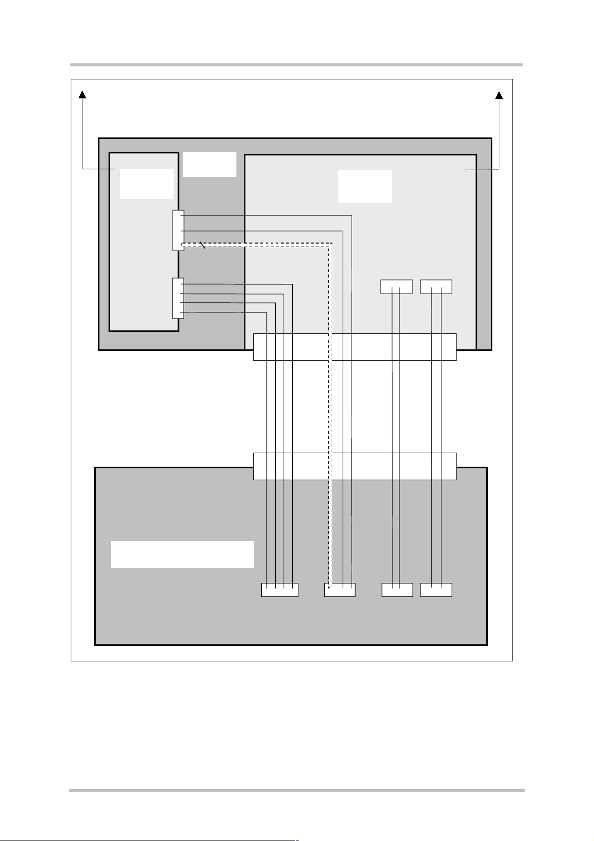
GSM antenna
GSM –
GSM module
Modul
ASC0
ASC1
XT 55
GSM_RXD0
GSM_TXD0
6 Modem
Status lines
GSM_RXD1
GSM_TXD1
GSM_RTS1
GSM_CTS1
Active GPS antenna
GPS –
GPS module
Modul
Serial data 2 Serial data 1
SDO2 SDI2
SDI1 SDO1
80 pin B2B
80 pin B2B
Serial 2
GPS
Serial 1
GPS
Customer application
Serial 1
GSM
Serial 0
GSM
Figure 1: Block diagram of serial interface concept
XT55_hd_v00.02 Page 23 of 116 15.03.2004
XT55 Hardware Interface Description
Confidential / Preliminary
s
mo b i l e
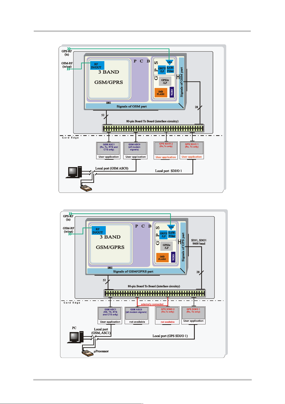
Figure 2: Block diagram of XT55 for SiRF Demo application
Figure 3: Block diagram of XT55 with AVL or TCP/IP application (optional)
XT55_hd_v00.02 Page 24 of 116 15.03.2004

XT55 Hardware Interface Description
Confidential / Preliminary
s
mo b i l e
3 GSM/GPRS application interface
The GSM/GPRS part of the XT55 module incorporates several sub-interfaces described in
the following chapters:
· Power supply and charging control (see Chapters 3.2 and 3.3)
· Dual serial GSM interface (see Chapter 3.9)
· Two analog audio interfaces and a digital audio interface (see Chapter 3.10)
· SIM interface (see Chapter 3.11)
Electrical and mechanical characteristics of the board-to-board connector are specified in
Chapter 7.3. Ordering information for mating connectors and cables are included.
3.1 GSM/GPRS operating modes
The table below briefly summarizes the various operating modes referred to in the following
chapters. All information regarding GPS operating modes are available in Chapter 4.3.
Table 3: Overview of GSM/GPRS operating modes
Mode Function
Normal operation
GSM / GPRS SLEEP Various powersave modes set with AT+CFUN
command.
Software is active to minimum extent. If the module was
registered to the GSM network in IDLE mode, it is
registered and paging with the BTS in SLEEP mode,
too. Power saving can be chosen at different levels: The
NON-CYCLIC SLEEP mode (AT+CFUN=0) disables the
AT interface. The CYCLIC SLEEP modes AT+CFUN=5,
6, 7, 8 and 9 alternatively activate and deactivate the AT
interfaces to allow permanent access to all AT
commands.
GSM IDLE Software is active. Once registered to the GSM network,
paging with BTS is carried out. The module is ready to
send and receive.
GSM TALK Connection between two subscribers is in progress.
Power consumption depends on network coverage
individual settings, such as DTX off/on, FR/EFR/HR,
hopping sequences, antenna.
GPRS IDLE Module is ready for GPRS data transfer, but no data is
currently sent or received. Power consumption depends
on network settings and GPRS configuration (e.g.
multislot settings).
GPRS DATA GPRS data transfer in progress. Power consumption
depends on network settings (e.g. power control level),
uplink / downlink data rates and GPRS configuration
(e.g. used multislot settings).
XT55_hd_v00.02 Page 25 of 116 15.03.2004

XT55 Hardware Interface Description
Confidential / Preliminary
s
mo b i l e
Mode Function
POWER DOWN Normal shutdown after sending the AT^SMSO command.
The Power Supply ASIC (PSU-ASIC) disconnects the supply voltage from the
baseband part of the circuit. Only a voltage regulator in the PSU-ASIC is active
for powering the RTC. Software is not active. The serial interfaces are not
accessible.
Operating voltage (connected to GSM_BATT+) remains applied.
Alarm mode Restricted operation launched by RTC alert function while the module is in
POWER DOWN mode. Module will not be registered to GSM network. Limited
number of AT commands is accessible.
Charge-only mode Limited operation for battery powered applications. Enables charging while
module is detached from GSM network. Limited number of AT commands is
accessible. There are several ways to launch Charge-only mode:
· From POWER DOWN mode: Connect charger to the charger input pin of the
external charging circuit and the module’s GSM_POWER pin when XT55
was powered down by AT^SMSO.
· From Normal mode: Connect charger to the charger input pin of the external
charging circuit and the module’s GSM_POWER pin, then enter AT^SMSO.
Charge mode
during normal
operation
Normal operation (SLEEP, IDLE, TALK, GPRS IDLE, GPRS DATA) and
charging running in parallel. Charge mode changes to Charge-only mode when
the module is powered down before charging has been completed.
See Table 11 and Table 12 for the various options of waking up the GSM/GPRS part of the XT55
module and proceeding from one mode to another.
XT55_hd_v00.02 Page 26 of 116 15.03.2004

XT55 Hardware Interface Description
Confidential / Preliminary
s
mo b i l e
3.2 Power supply
The power supply for the GSM/GPRS part of the XT55 module has to be a single voltage
source of V
GSM_BATT
burst which typically rises to 1.6A.
All the key functions for supplying power to the device are handled by an ASIC power
supply. The ASIC provides the following features:
· Stabilizes the supply voltages for the GSM baseband using low drop linear voltage
regulators.
· Controls the module's power up and power down procedures.
A watchdog logic implemented in the baseband processor periodically sends signals to
the ASIC, allowing it to maintain the supply voltage for all digital XT55 components.
Whenever the watchdog pulses fail to arrive constantly, the module is turned off.
· Delivers, across the GSM_VDD pin, a regulated voltage of 2.9V. The output voltage
GSM_VDD may be used to supply, for example, an external LED or a level shifter.
However, the external circuitry must not cause any spikes or glitches on voltage
GSM_VDD. This voltage is not available in POWER DOWN mode. Therefore, the
GSM_VDD pin can be used to indicate whether or not GSM/GPRS part of the XT55
module is in POWER DOWN mode.
· Provides power to the SIM interface.
The RF power amplifier is driven directly from GSM_BATT+.
+= 3.3V...4.8V. It must be able to provide sufficient current in a transmit
3.2.1 Power supply pins on the board-to-board connector
Five GSM_BATT+ pins of the board-to-board connector are dedicated to connect the supply
voltage, five GND pins are recommended for grounding. The values stated below must be
measured directly at the reference points on the XT55 board (TP GSM_BATT+ and TP GND
illustrated in Figure 52).
The GSM_POWER and GSM_CHARGE pins serve as control signals for charging a Li-Ion
battery. GSM_VDDLP can be used to back up the RTC.
Table 4: Power supply pins of board-to-board connector
Signal name I/O Description Parameter
GSM_BATT+ I/O Positive operating voltage
Reference points are the
test points
GND - Ground 0 V
GSM_POWER I This line signals to the
processor that the charger
is connected.
GSM_CHARGE O Control signal for external
charging transistor
GSM_VDDLP I/O Can be used to back up
the RTC when V
is not applied.
See Chapter 3.8
GSM_BATT+
3.3 V...4.8 V, I
The minimum operating voltage must not fall
below 3.3 V, not even in case of voltage drop.
U
UIN = 2.0 V...5.5 V
Ri = 1kW
I
in,max
OUT,max
= 30µA
< V
£ 1.6 A during transmit burst
typ
GSM_BATT+
XT55_hd_v00.02 Page 27 of 116 15.03.2004
XT55 Hardware Interface Description
Confidential / Preliminary
s
mo b i l e
3.2.2 Minimizing power losses
When designing the power supply for your application please pay specific attention to power
losses. Ensure that the input voltage V
GSM_BATT+
part of the XT55 board, not even in a transmit burst where current consumption can rise to
typical peaks of 1.6A. It should be noted that the GSM/GPRS part of the XT55 module
switches off when exceeding these limits. Any voltage drops that may occur in a transmit
burst should not exceed 400mV. For further details see Chapter 6.4.
The best approach to reducing voltage drops is to use a board-to-board connection as
recommended, and a low impedance power source. The resistance of the power supply lines
on the host board and of a battery pack should also be considered.
Note: If the application design requires an adapter cable between both board-to-board
connectors, use a cable as short as possible in order to minimize power losses.
Example: If the length of the cable reaches the maximum length of 200mm, this connection
may cause, for example, a resistance of 50m! in the GSM_BATT+ line and
50m! in the GND line. As a result, a 1.6A transmit burst would add up to a total
voltage drop of 160mV. Plus, if a battery pack is involved, further losses may
occur due to the resistance across the battery lines and the internal resistance of
the battery including its protective circuit.
never drops below 3.3V on the GSM/GPRS
Transmit
burst 1.6A
GSM_BATT+
min. 3.3V
Figure 4: Power supply limits during transmit burst
Transmit
burst 1.6A
Ripple
Drop
The input voltage V
GSM_BATT+
must be measured directly at the test points on the XT55 board
(TP GSM_BATT+ and TP GND illustrated in Figure 52).
3.2.3 Monitoring power supply
To help you monitor the supply voltage you can use the AT^SBV command which returns the
voltage measured at TP GSM_BATT+ and GND.
The voltage is continuously measured at intervals depending on the operating mode on the
RF interface. The duration of measuring ranges from 0.5s in TALK/DATA mode up to 50s
when the GSM/GPRS part of the XT55 is in IDLE mode or Limited Service (deregistered).
The displayed voltage (in mV) is averaged over the last measuring period before the
AT^SBV command was executed.
For details please refer to [1].
XT55_hd_v00.02 Page 28 of 116 15.03.2004

XT55 Hardware Interface Description
Confidential / Preliminary
s
mo b i l e
3.3 Power up / down scenarios
In general, be sure not to turn on GSM/GPRS part of the XT55 module while it is out of the
operating range of voltage and temperature stated in Chapters 6.2 and 6.3. The GSM/GPRS
part of the XT55 would immediately switch off after having started and detected these
inappropriate conditions.
3.3.1 Turn on the GSM/GPRS part of XT55
The GSM/GPRS part of the XT55 can be activated in a variety of ways, which are described
in the following chapters:
· via ignition line GSM_IGT: starts normal operating state (see Chapters 3.3.1.1 and
3.3.1.2)
· via GSM_POWER line: starts charging algorithm (see Chapters 3.5.4 and 3.3.1.3)
· via RTC interrupt: starts Alarm mode (see Chapter 3.3.1.4)
XT55_hd_v00.02 Page 29 of 116 15.03.2004
XT55 Hardware Interface Description
Confidential / Preliminary
s
mo b i l e
3.3.1.1 Turn on the GSM/GPRS part of XT55 using the ignition line GSM_IGT
(Power on)
To switch on the XT55 GSM/GPRS part the GSM_IGT (Ignition) signal needs to be driven to
ground level for at least 100ms and not earlier than 10ms after the last falling edge of
GSM_VDD. This can be accomplished using an open drain/collector driver in order to avoid
current flowing into this pin.
GSM_BATT+
min. 10ms
min.
GSM_IGT
HiZ
100ms
HiZ
GSM_VDD
GSM_TXD0
GSM_TXD1
GSM_DSR0
GSM_EMERGOFF
Serial interfaces
ASC0 and ASC1
For details please see Chapter 3.3.1.2
ca. 60ms
Software
controlled
Undefined
ca. 300ms ca. 900ms
Inactive
Active
Figure 5: Power-on by ignition signal
If configured to a fix baud rate, the GSM/GPRS part of the XT55 will send the result code
^SYSSTART to indicate that it is ready to operate. This result code does not appear when
autobauding is active. See Chapter AT+IPR in [1].
In a battery operated XT55 application, the duration of the GSM_IGT signal must be 1s
minimum when the charger is connected and you may want to go from Charge only mode to
Normal mode.
XT55_hd_v00.02 Page 30 of 116 15.03.2004
 Loading...