

Page 1
Cinterion® ALAS66A
Hardware Interface Description
Version: 01.000b
DocId: ALAS66A_HID_v01.000b
GEMALTO.COM/M2M
Page 2

Cinterion® ALAS66A Hardware Interface Description
2
Page 2 of 123
Document Name:
Version:
Date:
DocId:
Status
Cinterion
®
ALAS66A Hardware Interface Description
01.000b
2019-02-06
ALAS66A_HID_v01.000b
Confidential / Preliminary
GENERAL NOTE
THE USE OF THE PRODUCT INCLUDING THE SOFTWARE AND DOCUMENTATION (THE "PRODUCT") IS SUBJECT TO THE RELEASE NOTE PROVIDED TOGETHER WITH PRODUCT. IN ANY
EVENT THE PROVISIONS OF THE RELEASE NOTE SHALL PREVAIL. THIS DOCUMENT CONTAINS
INFORMATION ON GEMALTO M2M PRODUCTS. THE SPECIFICATIONS IN THIS DOCUMENT ARE
SUBJECT TO CHANGE AT GEMALTO M2M'S DISCRETION. GEMALTO M2M GMBH GRANTS A NONEXCLUSIVE RIGHT TO USE THE PRODUCT. THE RECIPIENT SHALL NOT TRANSFER, COPY,
MODIFY, TRANSLATE, REVERSE ENGINEER, CREATE DERIVATIVE WORKS; DISASSEMBLE OR
DECOMPILE THE PRODUCT OR OTHERWISE USE THE PRODUCT EXCEPT AS SPECIFICALLY
AUTHORIZED. THE PRODUCT AND THIS DOCUMENT ARE PROVIDED ON AN "AS IS" BASIS ONLY
AND MAY CONTAIN DEFICIENCIES OR INADEQUACIES. TO THE MAXIMUM EXTENT PERMITTED
BY APPLICABLE LAW, GEMALTO M2M GMBH DISCLAIMS ALL WARRANTIES AND LIABILITIES.
THE RECIPIENT UNDERTAKES FOR AN UNLIMITED PERIOD OF TIME TO OBSERVE SECRECY
REGARDING ANY INFORMATION AND DATA PROVIDED TO HIM IN THE CONTEXT OF THE DELIVERY OF THE PRODUCT. THIS GENERAL NOTE SHALL BE GOVERNED AND CONSTRUED
ACCORDING TO GERMAN LAW.
Copyright
Transmittal, reproduction, dissemination and/or editing of this document as well as utilization of its contents and communication thereof to others without ex press autho rization are prohib ited. Offenders will be
held liable for payment of damages. All rights created by patent grant or registration of a utility model or
design patent are reserved.
Copyright © 2019, Gemalto M2M GmbH, a Gemalto Company
Trademark Notice
Gemalto, the Gemalto logo, are trademarks and service marks of Gemalto and are registered in certain
countries. Microsoft and Win dows are e ither regis tered trademarks or trademarks of Microsoft Corporation in the United States and/or other countries. All other register ed trademarks or trademarks mention ed
in this document are property of their respective owners.
ALAS66A_HID_v01.000b 2019-02-06
Confidential / Preliminary
Page 3

Cinterion® ALAS66A Hardware Interface Description
Contents
123
Page 3 of 123
Contents
1 Introduction.................................................................................................................8
1.1 Product Variants ................................................................................................8
1.2 Key Features at a Glance..................................................................................9
1.2.1 Supported Frequency Bands.............................................................. 13
1.2.2 Supported CA Configurations............................................................. 14
1.3 System Overview.............................................................................................18
1.4 Circuit Concept ................................................................................................19
2 Interface Characteristics ..........................................................................................20
2.1 Application Interface ........................................................................................20
2.1.1 Pad Assignment..................................................................................20
2.1.2 Signal Properties.................................................................................24
2.1.2.1 Absolute Maximum Ratings ................................................31
2.1.3 USB Interface......................................................................................32
2.1.4 Serial Interface ASC0 .........................................................................33
2.1.5 Serial Interface ASC1 .........................................................................34
2.1.6 I
2.1.7 UICC/SIM/USIM Interface...................................................................36
2.1.8 Digital Audio Interface.........................................................................39
2.1.9 Analog-to-Digital Converter (ADC)......................................................40
2.1.10 RTC Backup........................................................................................40
2.1.11 GPIO Interface....................................................................................40
2.1.12 Control Signals....................................................................................42
2.1.13 JTAG Interface....................................................................................42
2.1.14 eMMC Interface ..................................................................................43
2.2 GSM/UMTS/LTE Antenna Interface.................................................................44
2.2.1 Antenna Interface Specifications ........................................................45
2.2.2 Antenna Installation ............................................................................50
2.2.3 RF Line Routing Design......................................................................51
2.2.4 RF Antenna Diagnostic.......................................................................54
2.3 GNSS Antenna Interface .................................................................................57
2.3.1 GNSS Antenna Diagnostic..................................................................58
2.4 Sample Application..................... ........... .......... ........... ........... ..........................59
2.4.1 Prevent Back Powering.......................................................................60
2.4.2 Sample Level Conversion Circuit........................................................61
2.4.3 Sample Circuit for Antenna Detection.................................................62
2
C Interface........................................................................................35
2.1.7.1 Enhanced ESD Protection for SIM Interfaces.....................38
2.1.8.1 Inter IC Sound Interface (I
2
S)..............................................39
2.1.11.1 External Antenna Switch Interface......................................41
2.1.12.1 PWR_IND Signal.................................................................42
2.1.12.2 Heartbeat Signal .................................................................42
2.1.14.1 eMMC Power Supply ..........................................................43
2.2.3.1 Line Arrangement Instructions ............................................51
2.2.3.2 Routing Examples...............................................................53
ALAS66A_HID_v01.000b 2019-02-06
Confidential / Preliminary
Page 4

Cinterion® ALAS66A Hardware Interface Description
Contents
123
Page 4 of 123
3 GNSS Interface..........................................................................................................65
3.1 GNSS Interface Characteristics.......................................................................66
4 Operating Characteristics........................................................................................67
4.1 Operating Modes .............................................................................................67
4.2 Power Up/Power Down Scenarios...................................................................68
4.2.1 Turn on ALAS66A...............................................................................68
4.2.2 Signal States after First Startup..........................................................69
4.2.3 Turn off or Restart ALAS66A..............................................................72
4.2.3.1 Switch off ALAS66A Using Shutdown Command................72
4.2.3.2 Restart ALAS66A Using Restart Command........................ 73
4.2.3.3 Turn off ALAS66A Using IGT Line.......................................74
4.2.3.4 Turn off or Restart ALAS66A in Case of Emergency...........75
4.2.3.5 Overall Shutdown Sequence...............................................76
4.2.4 Automatic Shutdown...........................................................................77
4.2.4.1 Thermal Shutdown..............................................................78
4.2.4.2 Deferred Shutdown at Extreme Temperature Conditions.... 79
4.2.4.3 Undervoltage Shutdown......................................................80
4.2.4.4 Overvoltage Shutdown........................................................80
4.3 Power Saving...................................................................................................81
4.3.1 Power Saving while Attached to GSM Networks................................81
4.3.2 Power Saving while Attached to WCDMA Networks ..........................82
4.3.3 Power Saving while Attached to LTE Networks..................................83
4.4 Power Supply...................................................................................................84
4.4.1 Power Supply Ratings.........................................................................85
4.4.2 Minimizing Power Losses ...................................................................92
4.4.3 Monitoring Power Supply by Configuration Setting.............................92
4.5 Operating Temperatures..................................................................................93
4.6 Electrostatic Discharge....................................................................................94
4.7 Reliability Characteristics.................................................................................94
5 Mechanical Dimensions and Mounting...................................................................95
5.1 Mechanical Dimensions of ALAS66A ..............................................................95
5.2 Mounting ALAS66A onto the Application Platform...........................................97
5.2.1 SMT PCB Assembly ...........................................................................97
5.2.1.1 Land Pattern and Stencil.....................................................97
5.2.1.2 Board Level Characterization..............................................98
5.2.2 Moisture Sensitivity Level ...................................................................99
5.2.3 Soldering Conditions and Temperature.............................................. 99
5.2.3.1 Reflow Profile......................................................................99
5.2.3.2 Maximum Temperature and Duration................................ 100
5.2.4 Durability and Mechanical Handling..................................................101
5.2.4.1 Storage Conditions............................................................101
5.2.4.2 Processing Life..................................................................101
5.2.4.3 Baking...............................................................................102
5.2.4.4 Electrostatic Discharge .....................................................102
ALAS66A_HID_v01.000b 2019-02-06
Confidential / Preliminary
Page 5

Cinterion® ALAS66A Hardware Interface Description
Contents
123
Page 5 of 123
5.3 Packaging......................................................................................................103
5.3.1 Trays.................................................................................................103
5.3.2 Shipping Materials ............................................................................103
5.3.2.1 Moisture Barrier Bag.........................................................103
5.3.2.2 Transportation Boxes........................................................105
6 Regulatory and Type Approval Information ......................................................... 106
6.1 Directives and Standards...............................................................................106
6.2 SAR requirements specific to portable mobiles............................................. 109
6.3 Reference Equipment for Type Approval.......................................................110
6.4 Compliance with FCC Rules and Regulations...............................................111
7 Document Information............................................................................................113
7.1 Revision History.............................................................................................113
7.2 Related Documents .......................................................................................117
7.3 Terms and Abbreviations...............................................................................117
7.4 Safety Precaution Notes................................................................................120
8 Appendix..................................................................................................................121
8.1 List of Parts and Accessories.........................................................................121
ALAS66A_HID_v01.000b 2019-02-06
Confidential / Preliminary
Page 6

Cinterion® ALAS66A Hardware Interface Description
Tables
123
Page 6 of 123
Tables
Table 1: Supported frequency bands for each ALAS66A variant................................. 13
Table 2: Supported CA configurations......................................................................... 14
Table 3: Overview: Pad assignments........................................................................... 21
Table 4: Signal description........................................................................................... 24
Table 5: Absolute maximum ratings............................................................................. 31
Table 6: DCE-DTE wiring of ASC0 .............................................................................. 34
Table 7: Signals of the SIM interface (SMT application interface)............................... 36
Table 8: Overview of I
Table 9: GPIO lines and possible alternative assignment............................................ 40
Table 10: GPIO lines and fixed alternative assignment................................................. 41
Table 11: Return loss in the active band........................................................................ 44
Table 12: RF Antenna interface GSM/UMTS/LTE (at operating temperature range) -
TBD................................................................................................................ 45
Table 13: Possible GPIOx signal states if used for antenna diagnosis.......................... 55
Table 14: Assured antenna diagnostic states................................................................ 56
Table 15: GSM/UMTS/LTE antenna diagnostic decision threshold............................... 56
Table 16: Sample ranges of the GNSS antenna diagnostic measurements and
their possible meaning................................................................................... 58
Table 17: Antenna detection reference circuit - parts list............................................... 64
Table 18: GNSS properties (TBD.) ................................................................................ 66
Table 19: Power supply for active GNSS antenna......................................................... 66
Table 20: Overview of operating modes ........................................................................ 67
Table 21: Signal states................................................................................................... 69
Table 22: Board temperature warning and switch off level............................................ 78
Table 23: Voltage supply ratings.................................................................................... 85
Table 24: Current consumption ratings (to be continued).............................................. 86
Table 25: Board temperature......................................................................................... 93
Table 26: Electrostatic values........................................................................................ 94
Table 27: Reflow temperature recommendations........................................................ 100
Table 28: Storage conditions ....................................................................................... 101
Table 29: Directives ..................................................................................................... 106
Table 30: Standards of North American type approval................................................ 106
Table 31: Standards of European type approval.......................................................... 106
Table 32: Requirements of quality ............................................................................... 107
Table 33: Standards of the Ministry of Information Industry of the
People’s Republic of China.......................................................................... 107
Table 34: Toxic or hazardous substances or elements with defined concentration
limits............................................................................................................. 108
Table 35: Antenna gain limits for FCC......................................................................... 111
Table 36: List of parts and accessories........................................................................ 121
Table 37: Molex sales contacts (subject to change).................................................... 122
Table 38: Hirose sales contacts (subject to change)................................................... 122
2
S pin functions......................................................................... 39
ALAS66A_HID_v01.000b 2019-02-06
Confidential / Preliminary
Page 7

Cinterion® ALAS66A Hardware Interface Description
Figures
123
Page 7 of 123
Figures
Figure 1: ALAS66A system overview............................................................................ 18
Figure 2: ALAS66A block diagram................................................................................ 19
Figure 3: ALAS66A bottom view: Pad assignments...................................................... 22
Figure 4: ALAS66A top view: Pad assignments............................................................ 23
Figure 5: USB circuit ..................................................................................................... 32
Figure 6: Serial interface ASC0..................................................................................... 33
Figure 7: Serial interface ASC1..................................................................................... 34
Figure 8: I
Figure 9: First UICC/SIM/USIM interface...................................................................... 37
Figure 10: SIM interfaces - enhanced ESD protection.................................................... 38
Figure 11: I
Figure 12: PWR_IND signal............................................................................................ 42
Figure 13: eMMC power supply ...................................................................................... 43
Figure 14: Antenna pads (top view)................................................................................ 50
Figure 15: Embedded Stripline line arrangement............................................................ 51
Figure 16: Micro-Stripline line arrangement samples...................................................... 52
Figure 17: Routing to application‘s RF connector ........................................................... 53
Figure 18: Routing detail................................................................................................. 53
Figure 19: Resistor measurement used for antenna detection....................................... 54
Figure 20: Basic circuit for antenna detection................................................................. 55
Figure 21: Supply voltage for active GNSS antenna....................................................... 57
Figure 22: ESD protection for passive GNSS antenna................................................... 58
Figure 23: ALAS66A sample application......................................................................... 60
Figure 24: Sample level conversion circuits.................................................................... 61
Figure 25: Antenna detection circuit sample - overview.................................................. 62
Figure 26: Antenna detection circuit sample - schematic................................................ 63
Figure 27: Power-on with IGT ......................................................................................... 68
Figure 28: Signal states during turn-off procedure.......................................................... 73
Figure 29: Timing of IGT if used as ON/OFF switch ....................................................... 74
Figure 30: Shutdown by EMERG_OFF signal................................................................. 75
Figure 31: Restart by EMERG_OFF signal..................................................................... 75
Figure 32: Overall shutdown sequence........................................................................... 76
Figure 33: Power saving and paging in GSM networks .................................................. 81
Figure 34: Power saving and paging in WCDMA networks............................................. 82
Figure 35: Power saving and paging in LTE networks.................................................... 83
Figure 36: Decoupling capacitor(s) for BATT+................................................................ 84
Figure 37: Power supply limits during transmit burst....................................................... 92
Figure 38: Board and ambient temperature differences.................................................. 93
Figure 39: ALAS66A – top and bottom view ................................................................... 95
Figure 40: Dimensions of ALAS66A (all dimensions in mm)........................................... 96
Figure 41: Land pattern (top layer).................................................................................. 97
Figure 42: Recommended design for 110 micron thick stencil (top layer)...................... 98
Figure 43: Reflow Profile................................................................................................. 99
Figure 44: Shipping tray dimensions............................................................................. 103
Figure 45: Moisture Sensitivity Label ............................................................................ 104
Figure 46: Humidity Indicator Card - HIC...................................................................... 105
Figure 47: Reference equipment for type approval....................................................... 110
2
C interface connected to VEXT ................................................................... 35
2
S timing (master mode) ............................................................................... 39
ALAS66A_HID_v01.000b 2019-02-06
Confidential / Preliminary
Page 8

Cinterion® ALAS66A Hardware Interface Description
1 Introduction
19
Page 8 of 123
1 Introduction
This document1 describes the hardware of the Cinterion® ALAS66A products listed in Section
1.1. It helps you quickly retrieve interface specifications, electrical and mechanical details and
information on the requirements to be considered for integrating further components.
1.1 Product Variants
This document applies to the following Gemalto M2M modules:
•Cinterion
•Cinterion
•Cinterion
•Cinterion
•Cinterion
•Cinterion
®
ALAS66A-W
®
ALAS66A-CN
®
ALAS66A-E
®
ALAS66A-US
®
ALAS66A-J
®
ALAS66A-K
Where necessary a note is made to differentiate between the various product variants and releases.
1. The document is effective only if listed in the appropriate Release Notes as part of the technical documentation delivered with your Gemalto M2M product.
ALAS66A_HID_v01.000b 2019-02-06
Confidential / Preliminary
Page 9
Cinterion® ALAS66A Hardware Interface Description
1.2 Key Features at a Glance
19
Page 9 of 123
1.2 Key Features at a Glance
Feature Implementation
General
Frequency bands Note: Not all of the frequency bands (and 3GPP technologies) me ntioned
throughout this document are supported by every ALAS66A products variant. Please refer to Section 1.2.1 for an overview of the frequency bands
supported by each ALAS66A product variant.
GSM class Small MS
Output power
(according to Release 99)
Output power
(according to Release 4)
Output power
(according to Release 8)
Power supply 3.3V <
Operating temperature
(board temperature)
Physical Dimensions: 48mm x 36mm x 3mm
RoHS All hardware components fully compliant with EU RoHS Directive
GSM/GPRS/UMTS:
Class 4 (+33dBm ±2dB) for EGSM850 and EGSM900
Class 1 (+30dBm ±2dB) for GSM1800 and GSM1900
Class E2 (+27dBm ± 3dB) for GSM 850 8-PSK and GSM 900 8-PSK
Class E2 (+26dBm +3 /-4dB) for GSM 1800 8-PSK and GSM 1900 8-PSK
Class 3 (+24dBm +1/-3dB) for all supported WCDMA FDD bands
TD-SCDMA:
Class 2 (+24dBm +1/-3dB) for TD-SCDMA 1900, TD-SCDMA Bd39 and
TD-SCDMA 2000, TD-SCDMA Bd34
LTE (FDD):
Class 3 (+23dBm +-2dB) for all supported LTE FDD bands
LTE (TDD):
Class 3 (+23dBm +-2dB) for all supported LTE TDD bands
V
Normal operation: -30°C to +85°C
Restricted operation: -40°C to +95°C
Weight: approx. 10.5g
BATT+
< 4.2V
ALAS66A_HID_v01.000b 2019-02-06
Confidential / Preliminary
Page 10
Cinterion® ALAS66A Hardware Interface Description
1.2 Key Features at a Glance
19
Feature Implementation
LTE features
3GPP Release 13 Downlink carrier aggregation (CA) to increase bandwidth, and thereby
increase bitrate:
• Maximum aggregated bandwidth: 80MHz
• Maximum number of component carriers: 3
• Inter-band FDD, TDD
• Intra-band FDD, TDD, contiguous, non-contiguous
• Supported inter- and intra-band CA configurations: See Section 1.2.2.
If 4x4 MIMO is supported by the mobile network:
• Downlink:
Up to 1Gbps CAT 16 with 4x4 MIMO 2 CA DL + 4(2)x2 MIMO 1 CA DL
or up to 800Mbps CAT 15 with 4x4 MIMO 2 CA DL
• Uplink:
Up to 150Mbps CAT 13 with 2 CA UL
If 4(2)x2 MIMO is supported by the mobile network:
• Downlink:
Up to 800Mbps CAT 15 with 4 CA DL
• Uplink:
Up to 150Mbps CAT 13 with 2 CA UL
Page 10 of 123
HSPA features
3GPP Release 8 UE CAT. 14, 24
DC-HSPA+ – DL 42Mbps
HSUPA – UL 5.76Mbps
Compressed mode (CM) supported according to 3GPP TS25.212
UMTS features
3GPP Release 8 PS data rate – 384 kbps DL / 384 kbps UL
TD-SCDMA features
3GPP Release 4 2.8 Mbps DL / 2.2Mbps UL
GSM / GPRS / EGPRS features
Data transfer GPRS:
• Multislot Class 12
• Mobile Station Class B
• Coding Scheme 1 – 4
EGPRS:
• Multislot Class 12
• EDGE E2 power class for 8 PSK
• Downlink coding schemes – CS 1-4, MCS 1-9
• Uplink coding schemes – CS 1-4, MCS 1-9
• SRB loopback and test mode B
• 8-bit, 11-bit RACH
• 1 phase/2 phase access procedures
• Link adaptation and IR
• NACC, extended UL TBF
• Mobile Station Class B
SMS Point-to-point MT and MO, Cell broadcast,
Text and PDU mode
ALAS66A_HID_v01.000b 2019-02-06
Confidential / Preliminary
Page 11
Cinterion® ALAS66A Hardware Interface Description
Page 11 of 123
1.2 Key Features at a Glance
19
Feature Implementation
Software
Embedded Linux platform Embedded Linux with API (ARC, RIL).
Memory space available for Linux applications is 4GB in the flash file sys-
tem, and 2GB RAM.
SIM Application Toolkit SAT Release 99, letter classes b, c, e with BIP and RunAT support
Firmware update Linux controlled firmware update.
GNSS Features
Protocol NMEA
Modes Standalone GNSS (GPS, GLONASS, Beidou, Galileo)
Integrated gpsOne 9HT support (GPS, GLONASS, Beidou, Galileo)
QZSS and SBAS support
General Power saving modes
DC feed bridge and control of power supply for active antenna via GPIO
Interfaces
Module interface Surface mount device with solderable connection pads (SMT application
interface).
Land grid array (LGA) technology ensures high solder joint reliability and
provides the possibility to use an optional module mounting socket.
For more information on how to integrate SMT modules see also [3]. This
application note comprises chapters on module mounting and app lication
layout issues as well as on additional SMT application development equip-
ment.
Antenna 50. 2 GSM/UMTS/LTE main antennas, 2 LTE Diversity/MIMO antennas,
(active/passive) GNSS antenna
USB USB 2.0 High Speed (480Mbit/s) device interface or
USB 3.0 Super Speed (5Gbit/s) device interface for debugging purposes
Serial interface Linux controlled:
ASC0:
• 4-wire (8-wire prepared) (plus GND line) interface unbalanced, asynchronous
• Fixed baud rates from 115,200 to 921,600bps
• Supports RTS0/CTS0 hardware flow control
ASC1:
• 4-wire, unbalanced asynchronous interface
• Fixed baud rates: 115,200bps to 921,60bps
• Supports RTS1/CTS1 hardware flow control
ASC2:
• 2-wire, unbalanced asynchronous interface at GPIO9 (RXD2) and
GPIO10 (TXD2) lines used for debugging purposes (optional)
UICC interface Supported chip cards: UICC/SIM/USIM 2.85V, 1.8V
2
I
C interfaces Linux controlled:
Audio 1 digital interface (I
2
2 I
C interfaces
2
S)
Power on/off, Reset
Power on/off Switch-on by hardware signal IGT
Automatic switch-off in case of critical temperature or voltage conditions
Emergency-off Emergency-off by hardware signal EMERG_OFF
ALAS66A_HID_v01.000b 2019-02-06
Confidential / Preliminary
Page 12
Cinterion® ALAS66A Hardware Interface Description
1.2 Key Features at a Glance
19
Feature Implementation
Special Features
Antenna SAIC (Single Antenna Interference Cancellation) / DARP (Downlink
Advanced Receiver Performance)
Rx Diversity (receiver type 3i - 64-QAM) / MIMO
HORxD (Higher Order Receive Diversity) with up to 4 antennas
GPIO Linux controlled:
18 I/O pins of the application interface programmable as GPIO.
External antenna switch 3 GPIOs permanently configured as optional external antenna switch inter-
face.
Emergency call handling EU eCall 3GPP Release 10 compliant (modem and GNSS)
ERA compliant (modem and GNSS)
ADC inputs Linux controlled:
Analog-to-Digital Converter with unbalanced analo g inputs for example for
(external) antenna diagnosis
JTAG JTAG interface for debug purposes
Page 12 of 123
eMMC Linux controlled:
Embedded Multi-Media Card interface
PCIe Linux controlled:
PCIe interface
Evaluation kit
Evaluation module ALAS66A module soldered onto a dedicated PCB.
ALAS66A_HID_v01.000b 2019-02-06
Confidential / Preliminary
Page 13
Cinterion® ALAS66A Hardware Interface Description
1.2 Key Features at a Glance
19
Page 13 of 123
1.2.1 Supported Frequency Bands
The following table lists the supported frequency bands for each of the ALAS66A product variants mentioned in Section 1.1.
Table 1: Supported frequency bands for each ALAS66A variant
Band -W -CN -E -US -J -K
GSM/GPRS/EDGE
850MHz x x x x
900MHz
1800MHz
1900MHz
UMTS/HSPA
Bd.I (2100MHz) x x x x x
Bd.II (1900MHz)
Bd.III (1800MHz)
Bd.IV (1700MHz)
Bd.V (850MHz)
Bd.VI (850MHz)
Bd.VIII (900MHz)
Bd.XIX (850MHz)
TD-SCDMA
Bd.34 (2000MHz) x
Bd.39 (1900MHz)
LTE-FDD
Bd.1 (2100MHz) x x x x x
x x x x x x
x x x x x x
x x x x
x
x x x x x
x
x x x x
x x x
x x x x x
x x x
x
Bd.2 (1900MHz)
Bd.3 (1800MHz)
Bd.4 (1700MHz)
Bd.5 (850MHz)
Bd.7 (2600MHz)
Bd.8 (900MHz)
Bd.12 (700MHz)
Bd.13 (700MHz)
Bd.18 (850MHz)
Bd.19 (850MHz)
Bd.20 (800MHz)
Bd.26 (850MHz)
Bd.28 (700MHz)
ALAS66A_HID_v01.000b 2019-02-06
x x x x x
x x x x
x x x x x x
x x x x x
x x x
x x x
x x x x
x x x
x x x x x
Confidential / Preliminary
x
x
x
x
Page 14
Cinterion® ALAS66A Hardware Interface Description
Page 14 of 123
1.2 Key Features at a Glance
19
Table 1: Supported frequency bands for each ALAS66A variant
Band -W -CN -E -US -J -K
Bd.29 (700MHz)
x
<supplementary
downlink>
Bd.30 (2300MHz)
1
x
<supplementary
downlink only acc.
FCC regulation>
Bd.32 (1500MHz)
x x x x
<supplementary
downlink>
Bd.66 (1700MHz)
x
LTE-TDD
Bd.34 (2000MHz) x x x x
Bd.38 (2600MHz)
Bd.39 (1900MHz)
Bd.40 (2300MHz)
Bd.41 (2600MHz)
1. Currently disabled by means of software because of AT&T regulation.
2. Note: Currently disabled for by means of software for the ALAS66A-W and ALAS66A-K variants. Also,
out of the 3GPP-specified frequency range for the LTE TDD Band 41 only the 110MHz frequency band
from 2545MHz to 2655MHz is supported by ALAS66A.
2
x x x x x
x x x x
x x x x
x x x x
1.2.2 Supported CA Configurations
The following table lists the supported CA configurations for each of the ALAS66A product variants mentioned in Section 1.1.
Table 2: Supported CA configurations
Downlink CA Uplink CA Bandwidth
combination set
Intra-band continuous
CA_1C - 0,1 E, W, CN, J, K
CA_2C - 0 US
CA_3C CA_3C 0 E, W, CN, J, K
CA_5B - 0,1 US, W, J, K
CA_7B - 0 E, US, W, CN, J, K
CA_7C CA_7C 0, 1, 2 E, US, W, CN, J, K
CA_8B - 0 E, W, CN, J, K
CA_12B - 0 US
CA_38C CA_38C 0 E, W, CN, J, K
CA_40C CA_40C 0, 1 W, CN, J, K
CA_40D - 0,1 W, CN, J, K
Product variants
(ALAS66A-...)
ALAS66A_HID_v01.000b 2019-02-06
Confidential / Preliminary
Page 15

Cinterion® ALAS66A Hardware Interface Description
1.2 Key Features at a Glance
19
Table 2: Supported CA configurations
Downlink CA Uplink CA Bandwidth
combination set
CA_41C CA_41C 0,1,2,3 CN, J
CA_41D CA_41C 0 CN, J
CA_66B - 0 US
CA_66C - 0 US
Intra-band non-continuous
CA_2A-2A - 0 US
CA_4A-4A - 0,1 US
CA_66A-66A - 0 US
Inter-band (two bands)
CA_1A-3A - 0,1 E, W, CN, J, K
CA_1A-3C CA_3C 0 E, W, CN, J, K
CA_1A-5A CA_1A-5A 0, 1 W
CA_1A-7A - 0 E, W, CN, J, K
CA_1A-8A CA_1A-8A 0, 1, 2 E, W, CN, J, K
CA_1A-18A CA_1A-18A 0, 1 W, J, K
CA_1A-19A - 0 W, J, K
CA_1A-20A - 0 E, W, J, K
CA_1A-26A CA_1A-26A 0, 1 W, J, K
CA_1A-28A CA_1A-28A 0, 1 E, W, J, K
CA_2A-2A-4A - 0 US
CA_2A-2A-4A-4A - 0 US
CA_2A-2A-5A - 0 US
CA_2A-2A-12A - 0 US
CA_2A-2A-13A - 0 US
CA_2A-2A-66A - 0 US
CA_2A-4A - 0, 1, 2 US
CA_2A-4A-4A - 0 US
CA_2A-5A - 0, 1 US
CA_2A-12A - 0, 1, 2 US
CA_2A-12B - 0 US
CA_2A-13A - 0, 1 US
CA_2A-28A - 0 US
CA_2A-29A - 0, 1, 2 US
CA_2A-66A - 0,1,2 US
CA_2A-66A-66A - 0 US
CA_2C-5A - 0 US
CA_2C-12A - 0 US
CA_2C-29A - 0 US
CA_3A-3A-8A CA_7C 0, 1 E, W, CN, J, K
CA_3A-5A CA_3A-8A 0, 1, 2, 3,4 W, J, K
CA_3A-7A - 0, 1 E, W, CN, J, K
CA_3A-7B CA_3A-20A 0 E, W, CN, J, K
Product variants
(ALAS66A-...)
Page 15 of 123
ALAS66A_HID_v01.000b 2019-02-06
Confidential / Preliminary
Page 16

Cinterion® ALAS66A Hardware Interface Description
1.2 Key Features at a Glance
19
Table 2: Supported CA configurations
Downlink CA Uplink CA Bandwidth
combination set
CA_3A-7C - 0, 1 E, W, CN, J, K
CA_3A-8A - 0, 1, 2, 3 E, W, CN, J, K
CA_3A-19A - 0 W, J, K
CA_3A-20A CA_3C 0, 1 E, W, J, K
CA_3A-26A - 0, 1 W, J, K
CA_3A-28A CA_3A-20A 0,1 E, W, J, K
CA_3C-5A - 0 W, J, K
CA_3C-7A - 0 E, W, CN, J, K
CA_3C-7C - 0,1 E, W, J, K
CA_3C-8A CA_3C-8A, CA_3C 0 W, J, K
CA_3C-20A - 0 E, W, J, K
CA_3C-28A - 0 E, W, J, K
CA_4A-4A-5A - 0 US
CA_4A-4A-7A - 0, 1 US
CA_4A-4A-12A - 0 US
CA_4A-4A-13A - 0 US
CA_4A-5A - 0, 1 US
CA_4A-7A - 0, 1 US
CA_4A-12A - 0,1,2,3,4,5 US
CA_4A-12B - 0 US
CA_4A-13A - 0, 1 US
CA_4A-28A - 0 US
CA_4A-29A - 0, 1, 2 US
CA_5A-7A CA_5A-7A 0, 1 US, W, J, K
CA_5A-12A - 0 US
CA_5A-66A - 0 US
CA_5A-66A-66A - 0 US
CA_7A-8A - 0, 1,2 E, W, CN, J, K
CA_7A-12A - 0 US
CA_7A-20A CA_7A-20A 0, 1 E, W, J, K
CA_7A-28A - 0, 1 E, US, W, J, K
CA_7B-28A - 0 E, US, W, J, K
CA_7C-28A CA_7C 0 E, US, W, J, K
CA_8A-20A - 0, 1 E, W, J, K
CA_12A-66A - 0,1,2,3,4,5 US
CA_12A-66A-66A - 0 US
CA_13A-66A - 0 US
CA_13A-66A-66A - 0 US
CA_18A-28A - 0 W, J, K
CA_20A-32A - 0,1 E, W, J, K
CA_39A-41A - 0 CN
CA_39A-41C CA_41C 0 CN
Product variants
(ALAS66A-...)
Page 16 of 123
ALAS66A_HID_v01.000b 2019-02-06
Confidential / Preliminary
Page 17

Cinterion® ALAS66A Hardware Interface Description
1.2 Key Features at a Glance
19
Table 2: Supported CA configurations
Downlink CA Uplink CA Bandwidth
combination set
CA_39C-41A CA_39C 0 CN
Inter-band (three bands)
CA_1A-3A-5A CA_1A-5A, CA_3A-5A 0, 1 E, W, J, K
CA_1A-3A-8A CA_1A-8A, CA_3A-8A 0,1,2,3 E, W, CN, J, K
CA_1A-3A-19A - 0 W, J, K
CA_1A-3A-20A CA_3A-20A 0 E, W, J, K
CA_1A-3A-26A - 0 W, J, K
CA_1A-3A-28A - 0 E, W, J, K
CA_1A-5A-7A CA_1A-5A, CA_5A-7A 0, 1 E, W, J, K
CA_1A-7A-8A - 0 E, W, CN, J, K
CA_1A-7A-20A - 0,1 E, W, J, K
CA_1A-7A-28A - 0,1,2 E, W, J, K
CA_1A-18A-28A - 0, 1 W, J, K
CA_1A-19A-28A - 0 W, J, K
CA_2A-2A-4A-12A - 0 US
CA_2A-2A-12A-66A - 0 US
CA_2A-4A-4A-12A - 0 US
CA_2A-4A-5A - 0 US
CA_2A-4A-12A - 0 US
CA_2A-4A-13A - 0 US
CA_2A-4A-29A - 0 US
CA_2A-5A-66A - 0 US
CA_2A-12A-66A - 0 US
CA_2A-12A-66A-66A - 0 US
CA_2A-13A-66A - 0 US
CA_3A-7A-8A CA_3A-8A 0, 1,2 E, W, CN, J, K
CA_3A-7A-28A - 0 E, W, J, K
CA_3A-7C-28A - 0 E, W, J, K
CA_4A-7A-12A - 0, 1 US
Product variants
(ALAS66A-...)
Page 17 of 123
ALAS66A_HID_v01.000b 2019-02-06
Confidential / Preliminary
Page 18
Cinterion® ALAS66A Hardware Interface Description
Power
Supply
IGT
EMERG_OFF
Application
Interfaces
ALAS66A
Application
VEXT
PWR_IND
Serial Interface
Digital
Audio
GNSS
Application
USIM
SIM
Card
Codec
GSM/UMTS/LTE
GPIO
Antenna-
diagnostic
4 x
ADC
I2S
I2C
I2C
Serial Interface
I2C
USB
2.0/3.0
ASC0
ASC1
I2C
Digital
Audio
GPIO
I2S
USB
Antenna-
diagnostic
External Antenna
Switch (optiona l)
TRX1 TRX2 RX3 RX4GNSS
GPIO
Power
Supply
eMMC
eMMC Interface
Power
Supply
PCIe
PCIe
3 x
ANT_SW
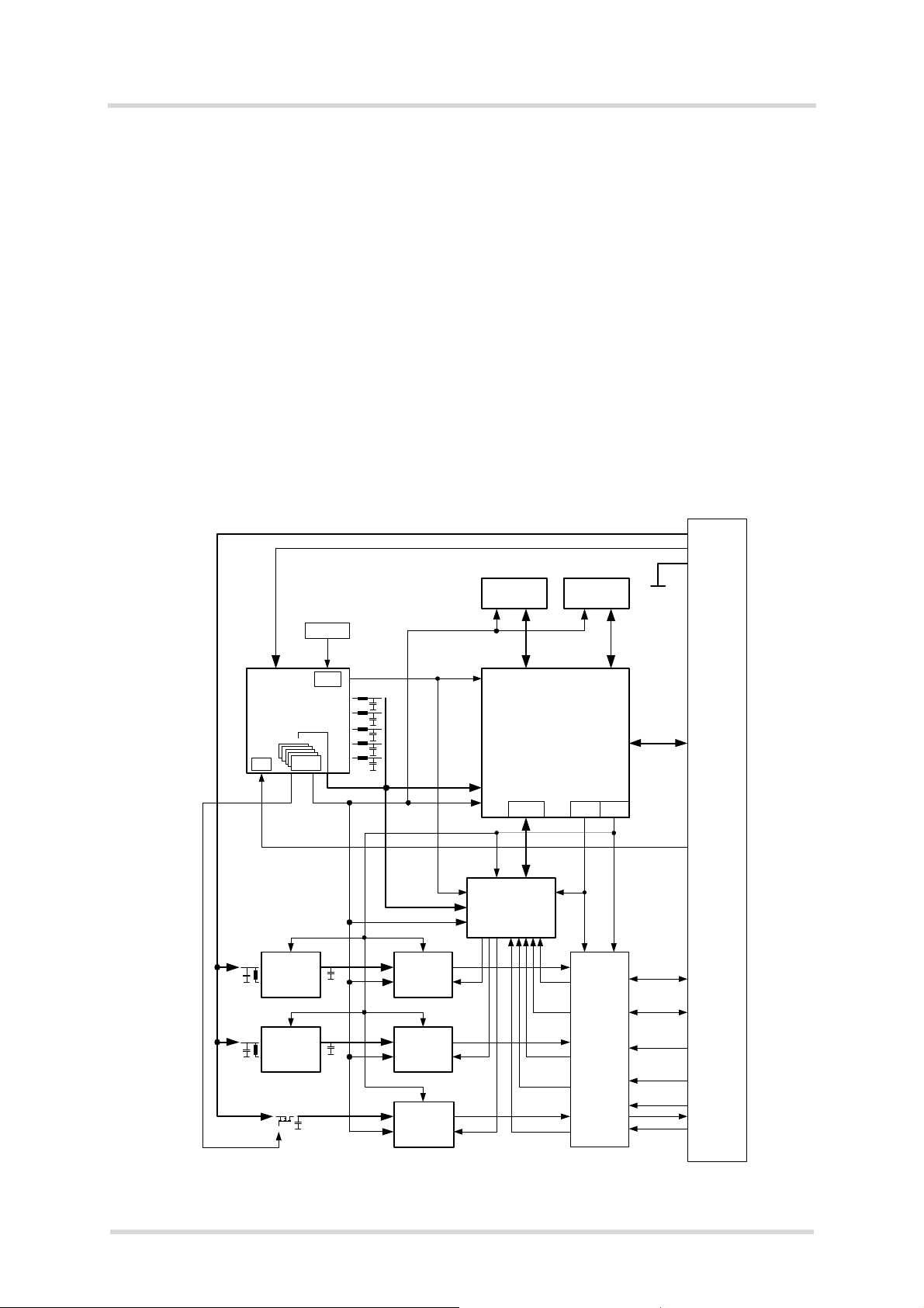
1.3 System Overview
19
1.3 System Overview
Page 18 of 123
Figure 1: ALAS66A system overview
ALAS66A_HID_v01.000b 2019-02-06
Confidential / Preliminary
Page 19
Cinterion® ALAS66A Hardware Interface Description
DDR2SDRAM
4GBi t
NANDFlash
8GBi t
38.4MHz
Powermanagement
Basebandcontroller
RFpart
Clocks
LDO
LDO
LDO
LDO
LDO
S1
S2
S3
S4
S5
PMU
PMU
MB/HB
PA
LB
PA
GSM
PA
Filter
&
Switches
QLINK RFFE
EBI 1
EBI 2
GRFC
BATT+
ANT_ TRX1
ANT_ TRX2
ANT_RX3
ANT_RX4
ANT_GNSS
GNSS_EN
ANT_GNSS_
C
LGAPads
IGT
EMERG _O FF
PWR_IND
USB 3.0
USB 2.0
ASC0
ASC1
2xI2C
I2S2
eMMC
SIM
GPIO
PCIe
4xADC_IN
ADC
BATT +_RF
GND
ALAS66A‐W
Page 19 of 123
1.4 Circuit Concept
19
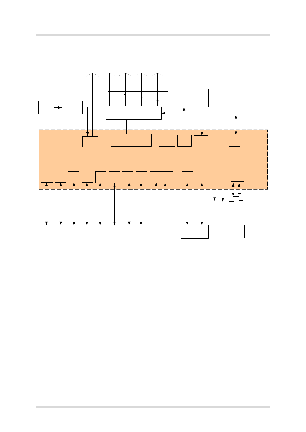
1.4 Circuit Concept
Figure 2 shows a block diagram of the ALAS66A module and illustrates the major functional
components:
Baseband block:
• GSM/UMTS/LTE controller/transceiver/power supply
• NAND/LPDDR2 memory devices
• A pplication interface (SMT with connecting pads)
RF section:
• RF transceiver
• RF power amplifier/frontend
• RF filter
• GNSS receiver/Front end
• Antenna pad
ALAS66A_HID_v01.000b 2019-02-06
Figure 2: ALAS66A block diagram
Confidential / Preliminary
D
Page 20

Cinterion® ALAS66A Hardware Interface Description
2 Interface Characteristics
66
Page 20 of 123
2 Interface Characteristics
ALAS66A is equipped with an SMT application interface that connects to the external application. The SMT application interface incorporates the various application interfaces as well as
the RF antenna interface.
2.1 Application Interface
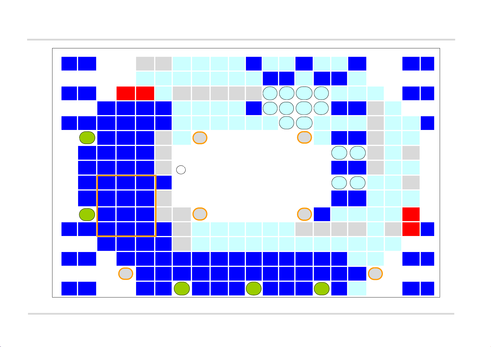
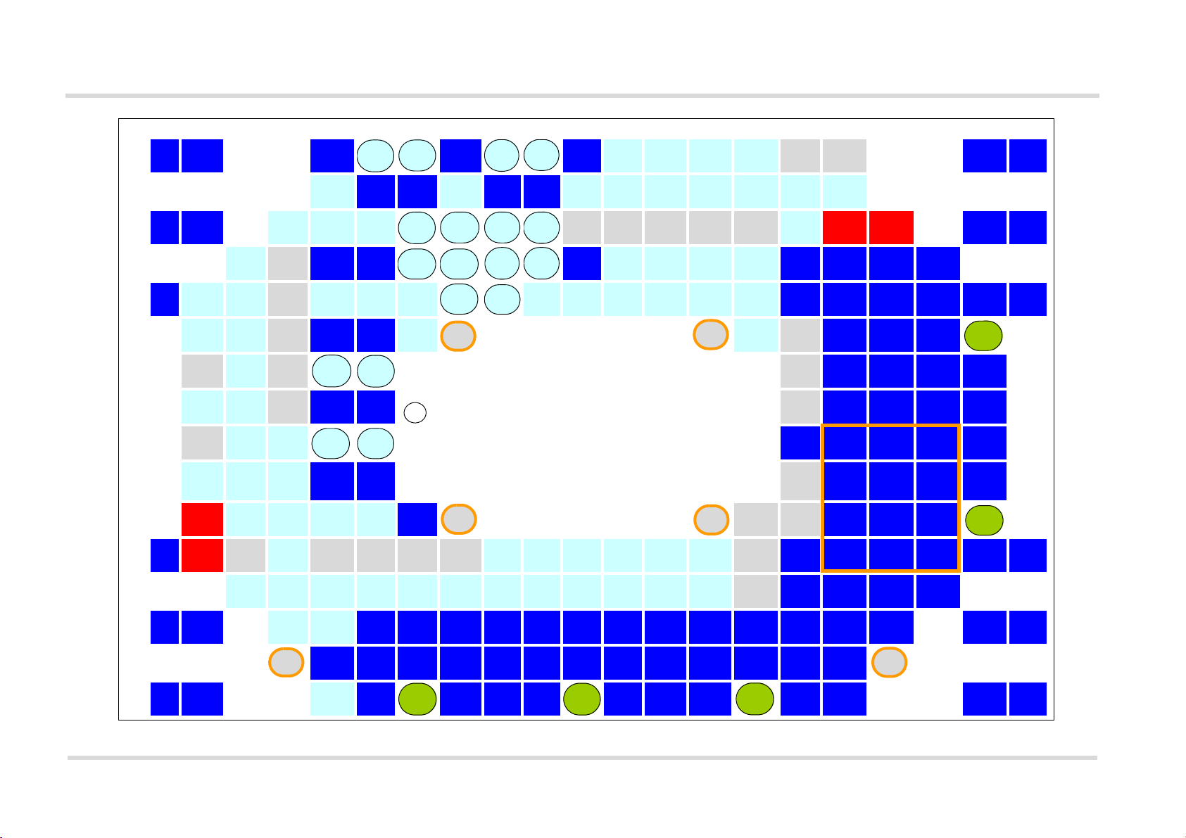
2.1.1 Pad Assignment
The SMT application interface on the ALAS66A provides connecting pads to integrate the module into external applications. Table 3 lists the pads’ assignments. Figure 3 (bottom view) and
Figure 4 (top view) show the connecting pads’ numbering plan.
Please note that a number of connecting pads are marked as reserved for future use (rfu) and
further qualified as either (<name>), (dnu), (GND) or (nc):
• Pads marked as “rfu“ and qualified as “<name>“ (signal name) may be soldered and could
be connected to an external application compliant to the signals’ electrical characteristics
as described in Table 4.
• Pads marked "rfu" and qualified as "dnu" (do not use) may be soldered but should not be
connected to an external application.
• Pads marked "rfu" and qualified as "GND" (ground) are assigned to ground with ALAS66A
modules, but may have different assignments with future Gemalto M2M p roducts using the
same pad layout.
• P ads marked "rfu" and qualified as "nc" (not connected) are internally not connected with
ALAS66A modules, but may be soldered and arbitrarily be connected to external ground.
Also note that some pads are marked with a circle ( ). These pads have a round shape for
improved impedance control.
Gemalto strongly recommends to solder all connecting pads for mechanical stability and heat
dissipation.
Also, Gemalto strongly recommends to provide test points for certain signal lines to and from
the module while developing SMT applications – for debug and/or test purposes during the
manufacturing process. In this way it is possible to detect soldering problems. Please refer to
[2] for more information on test points and how to implement them. The signal lines for which
test points should be provided for are marked as “Test point required” or “Test point recommended“ in Section 2.1.2: Table 4 describing signal characteristics.
ALAS66A_HID_v01.000b 2019-02-06
Confidential / Preliminary
Page 21
Cinterion® ALAS66A Hardware Interface Description
Page 21 of 123
2.1 Application Interface
66
Table 3: Overview: Pad assignments
Pad No. Signal Name Pad No. Signal Name Pad No. Signal Name
A1 GND E15 rfu (dnu) M8 JTAG_WD_DISABLE
A2 GND E16 rfu (dnu) M9 I2CDAT1
A5 GND E17 rfu (dnu) M10 I2CCLK1
A6 GND E18 VEXT M11 I2CDAT2
A7 ANT_RX3 E19 rfu (dnu) M12 I2CCLK2
A8 GND E20 BATT+ M13 EMMC_D6
A9 GND E21 GND M14 EMMC_D1
A10 GND F2 ANT_TRX2 M15 GPIO22 (Interrupt)
A11 ANT_RX4 F3 GND M16 USB_DP
A12 GND F4 GND M17 USB_DN
A13 GND F5 GND M18 rfu (dnu)
A14 GND F6 rfu (dnu) M19 CCCLK
A15 ANT_GNSS F7 rfu (dnu) M20 GPIO8 (Interrupt)
A16 GND F8 rfu (nc) M21 GND
A17 ANT_GNSS_DC F14 rfu (nc) N3 GND
A20 GND F15 GND
A21
B4
B5
B6
B7 GND F20 BATT+ N9 DIN2
B8
B9
B10 GND G4 GND N12 EMMC_D4
B11
B12
B13 GND G16 GND N15 EMMC_D0
B14 GND G17 GND N16 GND
B15 GND G18 GPIO20 / DCD0 / Download N17 GND
B16 GND G19 CTS0 N18 rfu (dnu)
B17 GND G20 RTS0 N19 CCIN
B18 rfu (dnu) H2 GND P1 GND
C1 GND H3 GND P2 GND
C2 GND H4 GND P4 BATT+_RF
C4 GND H5 GND P5 BATT+_RF
C5 GND H6 GND P6 GPIO5 (Interrupt)
C6 GND H16 USB_SSTX_P P7 rfu (DIN1)
C7 GND H17 USB_SSTX_N P8 rfu (DOUT1)
C8 GND H18 GPIO6 P9 rfu (BCLK1)
C9 GND H19 TXD0 P10 rfu (FSC1)
C10 GND H20 rfu (BATT_ID) P11 rfu (MCLK)
C11 GND J2 GND P12 EMMC_D7
C12 GND J3 GND P13 EMMC_CMD
C13 GND J4 GND P14 EMMC_D3
C14 GND J5 GND P15 EMMC_CLK
C15 GND J6 rfu (dnu) P16 PCIE_CLK_P
C16 GND J16 GND P17 PCIE_CLK_N
C17 HEART_BEAT J17 GND P18 VUSB_IN
C18 JTAG_TCK J18 rfu (dnu) P20 GND
C20 GND J19 CCIO P21 GND
C21 GND J20 GPIO19 / RING0 R5 PWR_IND
D3 GND K2 GND R6 RTS1
D4 GND K3 GND R7 CTS1
D5 GND K4 GND R8 TXD1
D6
D7
D8 ADC4_IN K16 USB_SSRX_P R11 PCIE_HOST_RST
D9
D10
D11
D12
D13 GNSS_EN L2 ANT_TRX1 R16 GND
D14 JTAG_TMS L3 GND R17 GPIO16 (Interrupt)
D15 JTAG_TRST L4 GND T1 GND
D16 JTAG_TDI L5 GND T2 GND
D17 JTAG_SRST L6 rfu (dnu) T5 rfu (dnu)
D18 JTAG_TDO L7 EMMC_DETECT T6 rfu (dnu)
D19 IGT L8 rfu (nc) T7 GPIO2 / FwSwap (Interrupt)
E1 GND L14 rfu (nc) T8 GPIO10 / TXD2 (Interrupt)
E2 GND L15 EMMC_PWR T9 GPIO15 / WLAN_EN
E3 GND L16 GND T10 GPIO9 / RXD2
E4 GND L17 GND T11 GND
E5 GND L18 rfu (dnu) T12 PCIE_RX_P
E6 GND L19 CCRST T13 PCIE_RX_N
E7 rfu (dnu) L20 GPIO4 T14 GND
E8 GPIO1/ DR_SYNC M1 GND T15 PCIE_TX_P
E9 GPIO7 (Interrupt) M2 GND T16 PCIE_TX_N
E10 ANT_SW3 M3 GND T17 GND
E11 ANT_SW2 M4 GND T20 GND
E12 ANT_SW1 M5 GND T21 GND
E13 JTAG_PS_HOLD M6 GND
E14 rfu (dnu) M7 GPIO17 / BT_EN
GND F16 EMERG_OFF
rfu (dnu) F17 GPIO18 / DSR0 N6 GND
GND F18 RXD0 N7 FSC2
GND F19 GPIO21 / DTR0 N8 DOUT2
GND G2 GND N10 BCLK2
GND G3 GND N11 GND
GND G5 GND N13 EMMC_D5
GND G6 rfu (dnu) N14 EMMC_D2
GND K5 GND R9 RXD1
rfu (dnu) K6 rfu (dnu) R10 PCIE_HOST_WAKE
ADC5_IN K17 USB_SSRX_N R12 GND
ADC1_IN K18 rfu (dnu) R13 GND
ADC2_IN K19 CCVCC R14 PCIE_CLK_REQ
GPIO11 K20 rfu (dnu) R15 GND
N4 GND
N5 GND
ALAS66A_HID_v01.000b 2019-02-06
Confidential / Preliminary
Page 22
Cinterion® ALAS66A Hardware Interface Description
1 2 3 4 5 6 7 8 9 101112131415161718192021
T
GND GND rfu
(dnu)
rfu
(dnu)
GPIO2 /
FwSWAP
(Interrupt)
GPIO10 /
TXD2
(Interrupt)
GPIO15 /
WLAN_E
N
GPIO9 /
RXD2
GND PCIE_
RX_P
PCIE_
RX_N
GND PCIE_
TX_P
PCIE_
TX_N
GND GND GND
R
PWR_
IND
RTS1 CTS1 TXD1 RXD1 PCIE_
HOST_
WAKE
PCIE_
HOST_
RST
GND GND PCIE_
CLK_
REQ
GND GND GPIO16
(Interrupt)
GND
P
GND GND BATT+_RFBATT+_RFGPIO5
(Inter-
rupt)
rfu
(DIN1)
rfu
(DOUT1)
rfu
(BCLK1)
rfu
(FSC1)
rfu
(MCLK)
EMMC_D7EMMC_
CMD
EMMC_D3EMMC_
CLK
PCIE_CLK_P
PCIE_
CLK_N
VUSB_
IN
GND GND
N
GND GND GND GND FSC2 DOUT2 DIN2 BCLK2 GND
EMMC_D4EMMC_D5EMMC_D2EMMC_
D0
GND GND rfu
(dnu)
CCIN GND
M
GND GND GND GND GND GND GPIO17 /
BT_EN
JTAG_
WD_
DISABLE
I2CDAT1 I2CCLK1I2CDAT2I2CCLK
2
EMMC_D6EMMC_
D1
GPIO22
(Inter-
rupt)
USB_DP USB_DN rfu
(dnu)
CCCLK GPIO8
(Interrupt)
GND
L
ANT_
TRX1
GND GND GND rfu
(dnu)
EMMC_
DETECT
rfu
(nc)
rfu
(nc)
EMMC_
PWR
GND GND rfu
(dnu)
CCRST GPIO4
K
GND GND GND GND rfu
(dnu)
USB_
SSRX_P
USB_
SSRX_N
rfu
(dnu)
CCVCC rfu
(dnu)
GND
J
GND GND GND GND rfu
(dnu)
GND GND rfu
(dnu)
CCIO GPIO19 /
RING0
GND
H
GND GND GND GND GND
USB_
SSTX_P
USB_
SSTX_N
GPIO6 TXD0 rfu
(BATT_
ID)
GND
G
GND GND GND GND rfu
(dnu)
GND GND GPIO20 /
DCD0 /
Down-
load
CTS0 RTS0 GND
F
ANT_
TRX2
GND GND GND rfu
(dnu)
rfu
(dnu)
rfu
(nc)
rfu
(nc)
GND EMERG
_OFF
GPIO18 /
DSR0
RXD0 GPIO21 /
DTR0
BATT+
E
GND GND GND GND GND GND rfu
(dnu)
GPIO1 /
DR_SYNC
GPIO7
(Inter-
rupt)
ANT_
SW3
ANT_
SW2
ANT_
SW1
JTAG_
PS_
HOLD
rfu
(dnu)
rfu
(dnu)
rfu
(dnu)
rfu
(dnu)
VEXT rfu
(dnu)
BATT+ GND
D
GND GND GND GND rfu
(dnu)
ADC4_IN ADC5_IN ADC1_INADC2_INGPIO11 GNSS_ENJTAG_
TMS
JTAG_
TRST
JTAG_
TDI
JTAG_
SRST
JTAG_
TDO
IGT
C
GND GND GND GND GND GND GND GND GND GND GND GND GND GND GND HEART_
BEAT
JTAG_
TCK
GND GND
B
rfu
(dnu)
GND GND GND GND GND GND GND GND GND GND GND GND GND
rfu
(dnu)
GND
A
GND GND GND GND
ANT_
RX3
GND GND GND
ANT_
RX4
GND GND GND
ANT_
GNSS
GND ANT_
GNSS_
DC
GND GND
rfu: Reserved for future use (may be connected to external application
(nc): Internally not connected (may be arbitrarily connected to external GND)
(dnu): Do not use (should not be connected to external application)
Circle marks round shaped pads designed for improved impedance.
Orange: Keep out areas on external application’s PCB.
Rectangular shaped: GND pads should be soldered, but no further tracks
on PCB’s 1
st
layer, as well as a solid ground plane on PCB’s 2nd layer.
Round shaped: No solder pads, should therefore not be soldered. No further tracks on PCB’s first layer.
2.1 Application Interface
66
Page 22 of 123
ALAS66A_HID_v01.000b 2019-02-06
Figure 3: ALAS66A bottom view: Pad assignments
Confidential / Preliminary
Page 23
Cinterion® ALAS66A Hardware Interface Description
21 20 19 18 17 16 15 14 13 12 11 10 9 8 7 6 5 4 3 2 1
T
GND GND GND
PCIE_
TX_N
PCIE_
TX_P
GND
PCIE_
RX_N
PCIE_
RX_P
GND GPIO9 /
RXD2
GPIO15 /
WLAN_E
N
GPIO10 /
TXD2
(Interrupt)
GPIO2 /
FwSwap
(Interrupt)
rfu
(dnu)
rfu
(dnu)
GND GND
R
GND GPIO16
(Interrupt)
GND GND PCIE_
CLK_
REQ
GND GND PCIE_
HOST_
RST
PCIE_
HOST_
WAKE
RXD1 TXD1 CTS1 RTS1 PWR_
IND
P
GND GND VUSB_INPCIE_
CLK_N
PCIE_CLK_P
EMMC_
CLK
EMMC_D3EMMC_
CMD
EMMC_
D7
rfu
(MCLK)
rfu
(FSC1)
rfu
(BCLK1)
rfu
(DOUT1)
rfu
(DIN1)
GPIO5
(Inter-
rupt)
BATT+_RFBATT+_
RF
GND GND
N
GND CCIN rfu
(dnu)
GND GND
EMMC_D0EMMC_D2EMMC_D5EMMC_
D4
GND BCLK2 DIN2 DOUT2 FSC2 GND GND GND GND
M
GND GPIO8
(Interrupt)
CCCLK rfu
(dnu)
USB_DN USB_DP GPIO22
(Inter-
rupt)
EMMC_D1EMMC_
D6
I2CCLK2I2CDAT2I2CCLK1I2CDAT1 JTAG_
WD_
DISABLE
GPIO17 /
BT_EN
GND GND GND GND GND GND
L
GPIO4 CCRST rfu
(dnu)
GND GND EMMC_
PWR
rfu
(nc)
rfu
(nc)
EMMC_
DETECT
rfu
(dnu)
GND GND GND
ANT_
TRX1
K
GND rfu
(dnu)
CCVCC rfu
(dnu)
USB_
SSRX_N
USB_
SSRX_P
rfu
(dnu)
GND GND GND GND
J
GND GPIO19 /
RING0
CCIO rfu
(dnu)
GND GND rfu
(dnu)
GND GND GND GND
H
GND rfu
(BATT_
ID)
TXD0 GPIO6
USB_
SSTX_N
USB_
SSTX_P
GND GND GND GND GND
G
GND RTS0 CTS0 GPIO20 /
DCD0 /
Down-
load
GND GND rfu
(dnu)
GND GND GND GND
F
BATT+ GPIO21 /
DTR0
RXD0 GPIO18 /
DSR0
EMERG
_OFF
GND
rfu
(nc)
rfu
(nc)
rfu
(dnu)
rfu
(dnu)
GND GND GND
ANT_
TRX2
E
GND BATT+ rfu
(dnu)
VEXT rfu
(dnu)
rfu
(dnu)
rfu
(dnu)
rfu
(dnu)
JTAG_
PS_
HOLD
ANT_
SW1
ANT_
SW2
ANT_
SW3
GPIO7
(Inter-
rupt)
GPIO1 /
DR_SYNC
rfu
(dnu)
GND GND GND GND GND GND
D
IGT JTAG_
TDO
JTAG_
SRST
JTAG_
TDI
JTAG_
TRST
JTAG_
TMS
GNSS_ENGPIO11 ADC2_INADC1_INADC5_IN ADC4_IN rfu
(dnu)
GND GND GND GND
C
GND GND JTAG_
TCK
HEART_
BEAT
GND GND GND GND GND GND GND GND GND GND GND GND GND GND GND
B
GND
rfu
(dnu)
GND GND GND GND GND GND GND GND GND GND GND GND GND
rfu
(dnu)
A
GND GND ANT_
GNSS_
DC
GND
ANT_
GNSS
GND GND GND
ANT_
RX4
GND GND GND
ANT_
RX3
GND GND GND GND
rfu: Reserved for future use (may be connected to external application
(nc): Internally not connected (may be arbitrarily connected to external GND)
(dnu): Do not use (should not be connected to external application)
Circle marks round shaped pads designed for improved impedance.
Orange: Keep out areas on external application’s PCB.
Rectangular shaped: GND pads should be soldered, but no further tracks
on PCB’s 1
st
layer, as well as a solid ground plane on PCB’s 2nd layer.
Round shaped: No solder pads, should therefore not be soldered. No further tracks on PCB’s first layer.
2.1 Application Interface
66
Page 23 of 123
ALAS66A_HID_v01.000b 2019-02-06
Figure 4: ALAS66A top view: Pad assig n me n ts
Confidential / Preliminary
Page 24
Cinterion® ALAS66A Hardware Interface Description
Page 24 of 123
2.1 Application Interface
66
2.1.2 Signal Properties
Please note that the reference voltages listed in Table 4 are the values measured directly on
the ALAS66A module. They do not apply to the accessories connected.
Table 4: Signal description
Function Signal name IO Signal form and level Comment
Power supply
External
supply voltage
BATT+
BATT+_RF
IV
max = 4.2V
I
V
min = 3.3V (on board)
I
Supply voltage lines for general power management and
the RF power amplifier.
GSM during Tx burst
Lines of BATT+/BATT+_RF
and GND respectively must
n Tx = n x 577µs peak current every
4.615ms
Imax = see Table 24
be connected in parallel for
supply purposes because
higher peak currents may
occur.
WCDMA TX continuous current
Imax = see Table 24
Minimum voltage must not
fall below 3.3V including
LTE TX continuous current
drop, ripple, spikes.
Imax = see Table 24
GND Ground Application Ground
VEXT O C
max = 1µF
L
VEXT may be used for application circuits.
V
= 1.80V -2.4%, +2%
O
If unused keep line open.
Normal operation:
I
max = -50mA
O
Test point recommended.
The external digital logic
SLEEP mode operation:
I
max = -1mA
O
must not cause any spikes
or glitches on voltage VEXT.
Supply voltage for
active
GNSS
antenna
(input)
External
GNSS supply voltage
enable
(output)
ANT_GNSS_DCIV
max = 5V
I
Imax = 50mA
GNSS_EN O V
max = 0.45V at I = 2mA
OL
V
nom = 0.1V at I = 100µA
OL
V
OH
V
OH
V
OH
min = 1.30V at I = -2mA
nom = 1.65V at I = -100µA
max = 1.84V
Do not exceed I
max in any
O
operation mode.
If unused connect to GND.
The input current must be
limited to 50mA (antenna
short circuit protection).
Enable signal for an external
voltage regulator (intended
for active GNSS antenna,
high=active)
No external pull-up allowed
during startup until the mod-
ule has been secured in fac-
tory.
ALAS66A_HID_v01.000b 2019-02-06
Confidential / Preliminary
Page 25
Cinterion® ALAS66A Hardware Interface Description
2.1 Application Interface
66
Table 4: Signal description
Function Signal name IO Signal form and level Comment
Page 25 of 123
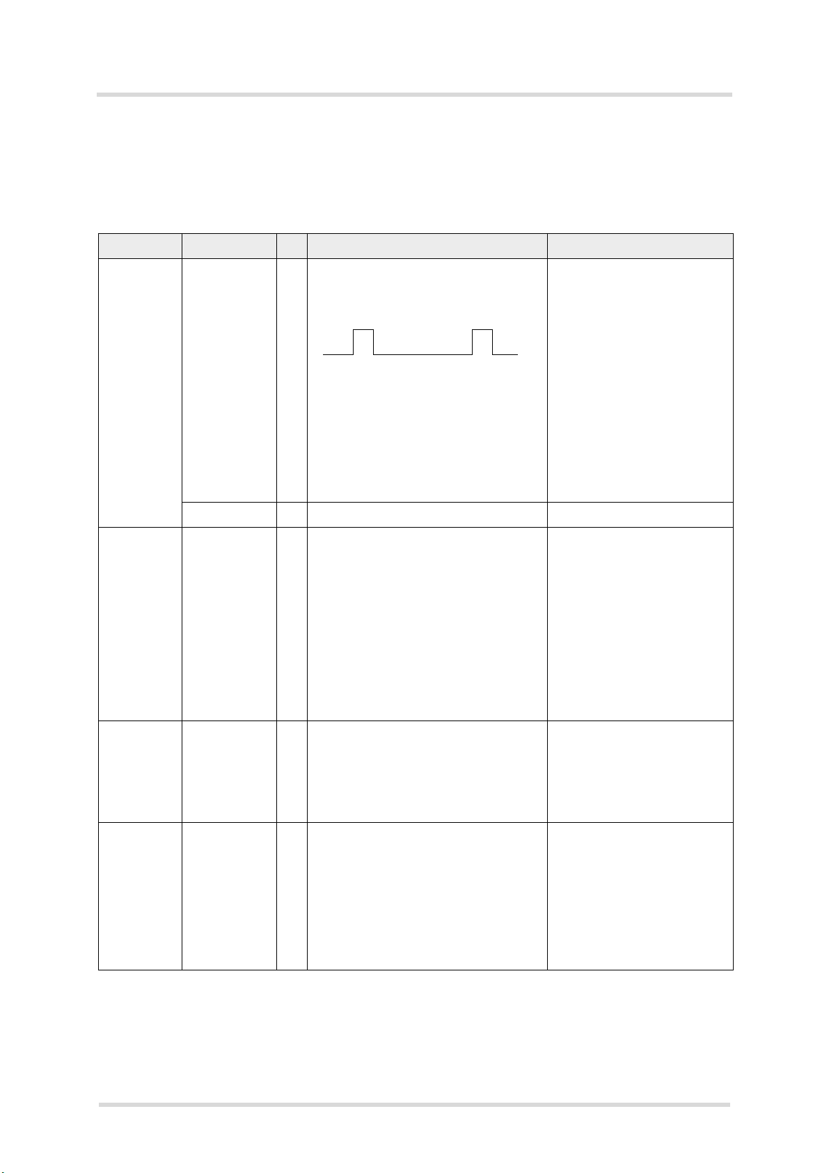
Ignition IGT I R
Emergency off
SIM card
EMERG_
IR
OFF
CCIN I R
detection
200k
PU
V
max = 1.84V
OH
V
max =2.00V
IH
V
min = 1.30V
IH
V
max = 0.50V
IL
Low impulse width > 100ms
40k
PU
V
max = 1.84V
OH
V
max = 2.00V
IH
V
min = 1.30V
IH
V
max = 0.50V
IL
¯¯|___|¯¯
low pulse width up to 2000ms
(as long as PWR_IND stays low
24kto VEXT
PU
V
max=1.84V
OH
V
min = 1.25V at -25µA
IH
V
max= 2.0V
IH
V
max = 0.35V at -60µA
IL
This signal switches the
module on.
It is required to drive this line
low by an open drain or open
collector driver connected to
GND.
Test point recommended.
It is required to drive this line
low by an open drain or open
collector driver connected to
GND until the module finally
switches off.
If unused keep line open.
Test point recommended.
Note that a low impulse of
more than 2000ms will reset
the module’s RTC.
CCIN = Low means SIM
card inserted.
If SIM card holder does not
support CCIN, connect to
GND.
2.85V SIM
card interfaces
CCRST O V
CCCLK
CCIO I/O R
CCVCC O V
max = 0.4V at I = 2mA
OL
V
nom = 0.1V at I = 100µA
OL
V
min = 2.2V at I = -2mA
OH
V
nom = 2.65V at I = -100µA
OH
V
max = 2.91V
OH
6.7..8.5k
PU
V
max = 0.55V
IL
V
min = 2.35V
IH
V
max = 3.05V
IH
V
max = 0.4V at I = 2mA
OL
V
nom = 0.1V at I = 100µA
OL
V
min = 2.35V at I > -45µA
OH
V
max = 2.91V
OH
min = 2.75V
O
V
typ =2.85V
O
V
max = 2.91V
O
I
max = -50mA
O
Maximum cable length or
copper track should be not
longer than 100mm to SIM
card holder.
If unused keep lines open.
ALAS66A_HID_v01.000b 2019-02-06
Confidential / Preliminary
Page 26
Cinterion® ALAS66A Hardware Interface Description
2.1 Application Interface
66
Table 4: Signal description
Function Signal name IO Signal form and level Comment
Page 26 of 123
1.8V SIM
card interface
SIM interface shutdown
Serial
Interface
ASC0
CCRST O V
CCCLK
CCIO I/O R
CCVCC O V
max = 0.4V at I = 2mA
OL
V
nom = 0.1V at I = 100µA
OL
V
min = 1.40V at I = -2mA
OH
V
min = 1.65V at I = -100µA
OH
V
max = 1.84V
OH
6.7..8.5k
PU
V
max = 0.30V
IL
V
min = 1.30V
IH
V
max = 1.84V
IH
V
max = 0.4V at I = 2mA
OL
V
nom = 0.1V at I = 100µA
OL
V
min = 1.40V at I > -50µA
OH
V
max = 1.84V
OH
min = 1.74V
O
V
typ = 1.80V
O
V
max = 1.84V
O
I
max = -50mA
O
BATT_ID I External pull up to VEXT and pull
down resistor within battery case
required.
R
= 100k
PU
R
= 10k
PD
RXD0 O V
CTS0 O
DSR0 O
RING0 O
max = 0.45V at I = 2mA
OL
V
nom = 0.1V at I = 100µA
OL
V
min = 1.30V at I = -2mA
OH
V
nom = 1.65V at I = -100µA
OH
V
max = 1.84V
OH
DCD0 I/O
TXD0 I V
RTS0 I
DTR0 I
max = 0.50V
IL
V
min = 1.30V
IH
V
max = 2.0V
IH
I
= 27.5µA…97.5µA
IHPD
I
= -27.5µA…-97.5µA
ILPU
I
High-Z max
= +-1µA
Maximum cable length or
copper track should be not
longer than 100mm to SIM
card holder.
If unused keep lines open.
Reserved for future use.
Connect line to GND.
Test points recommended
for TXD0, RXD0, DCD0,
RTS0, and CTS0.
If DCD0 is driven low during
startup-phase, module
enters Download Mode (see
Section 4.2.2)
If unused keep line open.
DSR0, DCD0, DTR0, and
RING0 are not yet imple-
mented, and are only avail-
able as GPIOs.
Serial
Interface
ASC1
RXD1 O V
CTS1 O
TXD1 I V
RTS1 I
max = 0.45V at I = 2mA
OL
V
nom = 0.1V at I = 100µA
OL
V
min = 1.30V at I = -2mA
OH
V
nom = 1.65V at I = -100µA
OH
V
max = 1.84V
OH
max = 0.50V
IL
V
min = 1.30V
IH
V
max = 2.0V
IH
I
= 27.5µA…97.5µA
IHPD
= -27.5µA…-97.5µA
I
ILPU
I
High-Z max
= +-1µA
Test points recommended
for RXD1, TXD1, CTS1, and
RTS1.
If unused keep line open.
ALAS66A_HID_v01.000b 2019-02-06
Confidential / Preliminary
Page 27
Cinterion® ALAS66A Hardware Interface Description
2.1 Application Interface
66
Table 4: Signal description
Function Signal name IO Signal form and level Comment
Page 27 of 123
Power indi-
PWR_IND O V
cator
USB VUSB_IN I V
max = 5.5V
IH
V
max = 0.45V at Imax = 2mA
OL
min = 3.0V
IN
V
max = 5.75V
IN
I
max = 100µA
I
Cin=1µF
PWR_IND (Power Indicator)
notifies the module’s on/off
state.
PWR_IND is an open collec-
tor that needs to be con-
nected to an external pull-up
resistor. Low state of the
open collector indicates that
the module is on. Vice versa,
high level notifies the Power
Down mode.
Therefore, the signal may be
used to enable external vol-
tage regulators that supply
an external logic for commu-
nication with the module,
e.g. level converters.
Test point recommended.
USB detection.
Test point recommended.
Digital
audio interface
2
(I
S)
USB_DN I/O Full and High speed signal (differenUSB_DP I/O
USB_
SSRX_N
USB_
tial) characteristics according to USB
2.0 specification.
I Super Speed signal (differential) Rx
characteristics according USB 3.0
specification.
I
SSRX_P
USB_
SSTX_N
USB_
O Super Speed signal (differential) Tx
characteristics according USB 3.0
specification.
O
SSTX_P
DIN2 I V
BCLK2 I/O
FSC2 I/O
DOUT2 O
max = 0.45V at I = 2mA
OL
V
nom = 0.1V at I = 100µA
OL
V
min = 1.30V at I = -2mA
OH
V
nom = 1.65V at I = -100µA
OH
V
max = 1.84V
OH
V
max = 0.50V
IL
V
min = 1.30V
IH
V
max = 2.0V
IH
= 27.5µA…97.5µA
I
IHPD
I
= -27.5µA…-97.5µA
ILPU
I
High-Z max
= +-1µA
If unused keep lines open.
Test point recommended.
USB High Speed mode
operation requires a differ-
ential impedance of 90
If unused keep lines open.
USB Super Speed mode
operation requires a differ-
ential impedance of 90
Digital audio interface con-
figurable as I
2
S interface.
If unused keep lines open.
ALAS66A_HID_v01.000b 2019-02-06
Confidential / Preliminary
Page 28
Cinterion® ALAS66A Hardware Interface Description
MUX,
ADC
module
1k
10n
ADCx_IN
2.1 Application Interface
66
Table 4: Signal description
Function Signal name IO Signal form and level Comment
Page 28 of 123
GPIO
interface
GPIO1...22 I/O V
max = 0.45V at I = 2mA
OL
V
nom = 0.1V at I = 100µA
OL
V
min = 1.30V at I = -2mA
OH
V
nom = 1.65V at I = -100µA
OH
V
max = 1.84V
OH
V
max = 0.50V
IL
V
min = 1.30V
IH
V
max = 2.0V
IH
I
= 27.5µA…97.5µA
IHPD
I
= -27.5µA…-97.5µA
ILPU
I
High-Z max
= +-1µA
GPIO2...GPIO5, GPIO7,
GPIO8, GPIO10, GPIO16,
and GPIO20...GPIO22 are
interrupt enabled. They can
be used to for instance wake
up the module (see Section
2.1.11).
GPIO12-14 are not imple-
mented, and only available
as external antenna switch
interface (see Section
2.1.11.1).
GPIO18-21 cannot be con-
figured as DSR0, DCD0,
DTR0, and RING0, because
this functionality is not yet
implemented.
No external pull-up / pull-
down resistors allowed for
GPIO9 and GPIO10.
There is a 2.2k decoupling
resistor between GPIO17
and JTAG_WD_DISABLE.
Heartbeat HEART_
BEAT
ADC
interface
ADC1_IN,
ADC2_IN,
ADC4_IN,
ADC5_IN
O
H --> L with 0.1Hz frequency, i.e.,
5s (+/- 1,5s) each for high and low
I Full specification compliance range
V
>=0.10V
Imin
V
<=1.70V
Imax
R
10M
I
Resolution: 14 Bit
Accuracy: <+-2mV
ADC conversion time t (max) = 550µs
at 4.8MHz sample clock
Test points recommended at
GPIO1, required at GPIO2,
GPIO9, and GPIO10.
If unused keep lines open.
However, GPIO7 and
GPIO17 must be low during
module startup until the
module has been secured in
factory.
Heartbeat signal, e.g., for
external watchdog.
If unused keep line open.
Prepared for general pur-
pose and antenna diagnos-
tic use.
ALAS66A_HID_v01.000b 2019-02-06
Confidential / Preliminary
Page 29
Cinterion® ALAS66A Hardware Interface Description
2.1 Application Interface
66
Table 4: Signal description
Function Signal name IO Signal form and level Comment
PCIe PCIE_RX_N I According to PCI Express Specifica-
PCIE_RX_P
PCIE_TX_N O
PCIE_TX_P
PCIE_CLK_N I/O
PCIE_CLK_P
tion, Revision 2.0/2.1 (one lane, 5
GBit/s)
Page 29 of 123
2
I
C inter-
face
JTAG interface
PCIE_-
IO V
CLK_REQ
PCIE_HOST_
O
RST
PCIE_HOST_
I
WAKE
I2CDAT1
I/O VILmax = 0.50V
I2CDAT2
I2CCLK1
O
I2CCLK2
JTAG_SRST I V
JTAG_TCK
JTAG_TDI
JTAG_TMS
JTAG_TRST
JTAG_TDO O
JTAG_WD_
IV
DISABLE
max = 0.45V at I = 2mA
OL
V
nom = 0.1V at I = 100µA
OL
V
min = 1.30V at I = -2mA
OH
V
nom = 1.65V at I = -100µA
OH
V
max = 1.84V
OH
V
max = 0.50V
IL
V
min = 1.30V
IH
V
max = 2.0V
IH
I
= 27.5µA…97.5µA
IHPD
I
= -27.5µA…-97.5µA
ILPU
I
High-Z max
V
V
V
V
I
ILPU
V
V
V
V
V
V
V
I
IHPD
I
ILPU
I
High-Z max
V
V
= +-1µA
min = 1.30V
IH
max = 2.0V
IH
max = 0.3V at I = 3mA
OL
max = 1.84V
OH
= -27.5µA…-97.5µA
max = 0.45V at I = 2mA
OL
nom = 0.1V at I = 100µA
OL
min = 1.30V at I = -2mA
OH
nom = 1.65V at I = -100µA
OH
max = 1.84V
OH
max = 0.50V
IL
min = 1.30V
IH
max = 2.0V
IH
= 27.5µA…97.5µA
= -27.5µA…-97.5µA
= +-1µA
max = 0.3V at -100µA
IL
min = 1.50V at 100µA
IH
max = 2.0V
IH
Additional PCIe control sig-
nals
Open Drain Output (internal
pull up)
External pull up resistors
required.
Maximum load 510Ohm.
Debug interface.
Test point recommended for
all JTAG lines.
High during reset and start-
up does disable the watch-
dog timer. (Jumper to VEXT)
There is a 2.2k decoupling
resistor between JTAG_
WD_DISABLE and GPIO17.
JTAG_
PS_HOLD
IV
min = 1.65V at 680µA
IH
V
max = 0.20V at 680µA
IL
High holds the power supply
during debugging
(Jumper to VEXT)
V
max = 1.84V
OH
V
min = 1.30V at 150µA
OH
max = 0.5V at -200µA
V
OL
ALAS66A_HID_v01.000b 2019-02-06
Confidential / Preliminary
Page 30
Cinterion® ALAS66A Hardware Interface Description
2.1 Application Interface
66
Table 4: Signal description
Function Signal name IO Signal form and level Comment
Page 30 of 123
eMMC
interface
1.8V
eMMC
2.95V
eMMC
EMMC_
IV
DETECT
EMMC_PWR O V
EMMC_CLK O V
EMMC_CMD O
EMMC_D[0...7]I/O
EMMC_CLK O V
EMMC_CMD O
EMMC_D[0...7]I/O
max = 0.45V at I = 2mA
OL
V
nom = 0.1V at I = 100µA
OL
V
min = 1.30V at I = -2mA
OH
V
nom = 1.65V at I = -100µA
OH
V
max = 1.84V
OH
V
max = 0.50V
IL
V
min = 1.30V
IH
V
max = 2.0V
IH
I
= 27.5µA…97.5µA
IHPD
I
= -27.5µA…-97.5µA
ILPU
I
High-Z max
I
OUT (max)
V
V
V
V
V
I
High-Z max
V
V
V
V
V
I
High-Z max
= +-1µA
OUT (nom)
= 2.95V / 1.8V
= 150mA
max = 0.45V at rated drive strength
OL
min = 1.40V at rated drive strength
OH
max = 1.84V
OH
max = 0.58V at rated drive strength
IL
min = 1.27V at rated drive strength
IH
max = 2.0V
IH
= +-5µA
max = 0.36V at rated drive strength
OL
min = 2.05V at rated drive strength
OH
max = 2.91V
OH
max = 0.68V at rated drive strength
IL
min = 1.82V at rated drive strength
IH
max = 3.05V
IH
= +-10µA
eMMC
ALAS66A_HID_v01.000b 2019-02-06
Confidential / Preliminary
Page 31

Cinterion® ALAS66A Hardware Interface Description
2.1 Application Interface
66
Page 31 of 123
2.1.2.1 Absolute Maximum Ratings
The absolute maximum ratings stated in Table 5 are stress ratings under any conditions.
Stresses beyond any of these limits will cause permanent damage to ALAS66A.
Table 5: Absolute maximum ratings
Parameter Min Max Unit
Supply voltage BATT+ -0.3 +5.5 V
Voltage at all digital lines in Power Down mode (except VEXT) -0.3 +0.5 V
Voltage at VEXT in Power Down mode -0.3 +0.3 V
Voltage at digital lines in normal operation -0.3 +2.3 V
Voltage at SIM/USIM interface, CCVCC 1.8V in normal operation -0.3 +2.3 V
Voltage at SIM/USIM interface, CCVCC 3.0V in normal operation -0.3 +3.4 V
Voltage at ADC lines if the module is powered by BATT+ -0.5 V
Voltage at ADC lines if the module is not powered -0.5 +0.5 V
VEXT maximum current shorted to GND -600 mA
VUSB_IN -0.3 5.75 V
USB 3.0 data lines -0.3 +1.4 V
USB 2.0 data lines -0.3 +3.6 V
PCIe data and clock lines -0.3 +1.4 V
PCIe control lines -0.3 +2.1 V
Voltage at PWR_IND line -0.5 +5.5 V
PWR_IND input current if PWR_IND= low 2 mA
Voltage at following signals:
IGT, EMERG_OFF
-0.3 2.1 V
BATT+
+0.5V V
ALAS66A_HID_v01.000b 2019-02-06
Confidential / Preliminary
Page 32

Cinterion® ALAS66A Hardware Interface Description
BATT+
USB_DP
c)
lin. reg.
GND
Module
Detection only
VUSB_IN
b)
USBpart
a)
a)
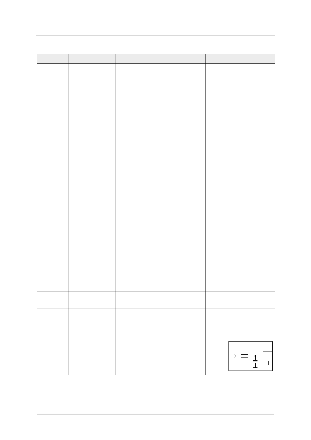
All serial (including RS) and pull-up resistors for data lines are implemented .
USB_DN
c)
c)
If the USB interface is operated with super or high speeds, it is recom mended to ta ke speci a l care routing the data
lines. Application layout should implement a differential impedance of 90 ohms for proper signal integrity .
VBUS
1µF
b)
Since VUSB_IN is used for detection only it is recommended not to add any further blocking capacitors on
the VUSB_IN line .
USB_SSRX_N
c)
USB_SSRX_P
c)
USB_SSTX_N
c)
USB_SSTX_P
c)
USB_SS
_PHY
USB_HS
_PHY
USB 2.0
Controller
USB 3.0
Controller
2.0
2.0
3.0
100nF
100nF
SMT
Page 32 of 123
2.1 Application Interface
66
2.1.3 USB Interface
ALAS66A supports a USB 3.0 Super Speed (5Gbps) device interface, and alternatively a USB
2.0 device interface that is High Speed compatible. The USB interface is primarily intended f or
use as debugging interface.
The USB host is responsible for supplying the VUSB_IN line. This line is for voltage detection
only. The USB part (driver and transceiver) is supplied by means of BATT+. This is because
ALAS66A is designed as a self-powered device compliant with the “Universal Serial Bus Specification Revision 3.0”
1
.
Figure 5: USB circuit
To properly connect the module's USB interface to the external application, a USB 3.0 or 2.0
compatible connector and cable or hardware design is required. For further guidelines on implementing the external application’s USB 3.0 or 2.0 interface see [3] and [4]. For more information on the USB related signals see Table 4. Furthermore, the USB driver distributed with
ALAS66A needs to be installed.
While a USB connection is active, the module will never switch into SLEEP mode. Only if the
USB interface is in Suspended state or Detached (i.e., VUSB_IN = 0) is the module able to
switch into SLEEP mode thereby saving power
1. The specification is ready for download on http://www.usb.org/developers/docs/
2. Please note that if the USB interface is employed, and a USB cable is connected, there should also be
a terminal program linked to the USB port in order to receive and process the initial SYSSTART URC
after module startup. Otherwise, the SYSSTART URC remains pending in the USB driver's output buffer
and this unprocessed data prevents the module from power saving.
ALAS66A_HID_v01.000b 2019-02-06
2
.
Confidential / Preliminary
Page 33

Cinterion® ALAS66A Hardware Interface Description
2.1 Application Interface
66
Page 33 of 123
2.1.4 Serial Interface ASC0
ALAS66A offers a 4-wire (8-wire prepared) (plus GND) unbalanced, asynchronous interface
ASC0 conforming to ITU-T V.24 protocol DCE signaling. The electrical characteristics do not
comply with ITU-T V.28. The significant levels are 0V (for low data bit or active state) and 1.8V
(for high data bit or inactive state). For electrical characteristics please refer to Table 4.
ALAS66A is designed for use as a DCE. Based on the conventions for DCE-DTE connections
it communicates with the customer application (DTE) using the following signals:
• Port TXD @ application sends data to the module’s TXD0 signal line
• Port RXD @ application receives data from the module’s RXD0 signal line
Figure 6: Serial interface ASC0
Features:
• Includes the data lines TXD0 and RXD0, the status lines RTS0 and CTS0. The modem control lines DTR0, DSR0, DCD0 and RING0 are not yet implemented.
• The RING0 signal serves to indicate incoming calls and other types of URCs (Unsolicited
Result Code). It can also be used to send pulses to the host application, for example to
wake up the application from power saving state. Not yet implemented.
• Configured for 8 data bits, no parity and 1 stop bit.
• ASC0 can be operated at fixed bit rates from 115,200 to 921,600bps.
• S upports RTS0/CTS0 hardware flow control.
Note: If the ASC0 serial interface is the application’s only interface, it is suggested to connect
test points on the USB signal lines as a potential tracing possibility.
ALAS66A_HID_v01.000b 2019-02-06
Confidential / Preliminary
Page 34

Cinterion® ALAS66A Hardware Interface Description
2.1 Application Interface
66
Table 6: DCE-DTE wiring of ASC0
V.24 circuit DCE DTE
Line function
103 TXD0 Input TXD Output
104 RXD0 Output RXD Input
105 RTS0 Input RTS Output
106 CTS0 Output CTS Input
108/2 DTR0 Input DTR Output
107 DSR0 Output DSR Input
109 DCD0 Output DCD Input
125 RING0 Output RING Input
1. DSR0, DCD0, DTR0, and RING0 not yet implemented
1
Signal direction Line function Signal direction
Page 34 of 123
2.1.5 Serial Interface ASC1
Four ALAS66A lines can be configured as ASC1 interface signals to provide a 4-wire unbalanced, asynchronous interface ASC1 conforming to ITU-T V.24 protocol DCE signaling. The
electrical characteristics do not comply with ITU-T V.28. The significant levels are 0V (for low
data bit or active state) and 1.8V (for high data bit or inactive state). For electrical characteristics please refer to Table 3.
ALAS66A is designed for use as a DCE. Based on the conventions for DCE-DTE connections
it communicates with the customer application (DTE) using the following signals:
• Port TXD @ application sends data to module’s TXD1 signal line
• Port RXD @ application receives data from the module’s RXD1 signal line
Figure 7: Serial interface ASC1
Features
• Includes only the data lines TXD1 and RXD1 plus RTS1 and CTS1 for hardware handshake.
• On ASC1 no RING line is available.
• Configured for 8 data bits, no parity and 1 or 2 stop bits.
• ASC1 can be operated at fixed bit rates from 115,200 bps to 921,600 bps.
• S upports RTS1/CTS1 hardware flow.
ALAS66A_HID_v01.000b 2019-02-06
Confidential / Preliminary
Page 35

Cinterion® ALAS66A Hardware Interface Description
I2CCLK
I2CDAT
GND
I2CCLK
I2CDAT
GND
Module Application
VEXT
R pull up
R pull up
Page 35 of 123
2.1 Application Interface
66
2.1.6 I2C Interface
ALAS66A provides two I2C interfaces. I2C is a serial, 8-bit oriented data transfer bus for bit rates
up to 400kbps in Fast mode. It consists of two lines, the serial data line I2CDAT and the serial
clock line I2CCLK. The module acts as a single master device, e.g. the clock I2CCLK is driven
by the module. I2CDAT is a bi-directional line. Each device connected to the bus is software
addressable by a unique 7-bit address, and simple master/slave relationships exist at all times.
The module operates as master-transmitter or as master-receiver. The customer application
transmits or receives data only on request of the module.
The applications I
the VEXT line, the I
2
C interface can be powered via the VEXT line of ALAS66A. If connected to
2
C interface will properly shut down when the module enters the Power
Down mode.
In the application I2CDATx and I2CCLKx lines need to be connected to a positive supply volt-
age (e.g., VEXT) via a pull-up resistor. For electrical characteristics please refer to Table 4.
Figure 8: I2C interface connected to VEXT
Note: Good care should be taken when creating the PCB layout of the host application: The
traces of I2CCLK and I2CDAT should be equal in length and as short as possible.
ALAS66A_HID_v01.000b 2019-02-06
Confidential / Preliminary
Page 36

Cinterion® ALAS66A Hardware Interface Description
2.1 Application Interface
66
Page 36 of 123
2.1.7 UICC/SIM/USIM Interface
ALAS66A has a UICC/SIM/USIM interface compatible with the 3GPP 31.102 and ETSI 102
221. It is wired to the host interface in order to be connected to an external SIM card holder.
Five pads on the SMT application interface are reserved for the SIM interface.
The UICC/SIM/USIM interface supports 2.85V and 1.8V SIM cards. Please refer to Table 4 for
electrical specifications of the UICC/SIM/USIM interface lines depending on whether a 2.85V
or 1.8V SIM card is used.
The CCIN signal serves to detect whether a tray (with SIM card) is present in the card holder.
Using the CCIN signal is mandatory for compliance with the GSM 11.11 recommendation if the
mechanical design of the host application allows the user to remove the SIM card during operation. To take advantage of this feature, an appropriate SIM card detect switch is required on
the card holder. For example, this is true for the model supplied by Molex, which has been tested to operate with ALAS66A and is part of the Gemalto M2M reference equipment submitted
for type approval. See Chapter 8 for Molex ordering numbers.
Table 7: Signals of the SIM interface (SMT application interface)
Signal Description
GND Ground connection for SIM interfaces. Optionally a separate SIM ground line may be used
to improve EMC.
CCCLK Chipcard clock line for SIM interface.
CCVCC SIM supply voltage line for SIM interface.
CCIO Serial data line for SIM interface, input and output.
CCRST Chipcard reset line SIM interface.
CCIN Input on the baseband processor for detecting a SIM card tray in the holder. If the SIM is
removed during operation the SIM interface is shut down immediately to prevent destruc-
tion of the SIM. The CCIN signal is active low.
The CCIN signal is mandatory for applications that allow the user to remove the SIM card
during operation.
The CCIN signal is solely intended for use with a SIM card. It must not be used for any other
purposes. Failure to comply with this requirement may invalidate the type approval of
ALAS66A.
Note: No guarantee can be given, nor any liability accepted, if loss of data is encountered after
removing the SIM card during operation. Also, no guarantee can be given for properly initializing any SIM card that the user inserts after having removed the SIM card during operation. In
this case, the application must restart ALAS66A.
ALAS66A_HID_v01.000b 2019-02-06
Confidential / Preliminary
Page 37

Cinterion® ALAS66A Hardware Interface Description
Module
open: Card removed
closed : C ar d insert ed
CCRST
CCVCC
CCIO
CCCLK
CCIN
SIM /
UICC
1n
220n
SMT applicat ion interface
GND
2.1 Application Interface
66
Figure 9: First UICC/SIM/USIM interface
Page 37 of 123
The total cable length between the SMT application interface pads on ALAS66A and the p ads
of the external SIM card holder must not exceed 100mm in order to meet the specifications of
3GPP TS 51.010-1 and to satisfy the requirements of EMC compliance.
To avoid possible cross-talk from the CCCLK signal to the CCIO signal be careful that both
lines are not placed closely next to each other. A useful approach is using the GND line to
shield the CCIO line from the CCCLK line.
An example for an optimized ESD protection for the SIM interface is shown in Section 2.1.7.1 .
ALAS66A_HID_v01.000b 2019-02-06
Confidential / Preliminary
Page 38

Cinterion® ALAS66A Hardware Interface Description
CCRST
CCCLK
CCIO
CCVCC
CCIN
51R
51R
51R
123
654
SIM_RST
SIM_CLK
SIM_IO
SIM_VCC
SIM_DET
Module
GND SIM_GND
5-line transient voltage
supressor array, e.g.,
NU P4114 series
Page 38 of 123
2.1 Application Interface
66
2.1.7.1 Enhanced ESD Protection for SIM Interfaces
To optimize ESD protection for the SIM interfaces it is possible to add ESD diodes to the interface lines of the first and second SIM interface as shown in the example given in Figure 10.
The example was designed to meet ESD protection according ETSI EN 301 489-1/ 7: Contact
discharge: ± 4kV, air discharge: ± 8kV.
Figure 10: SIM interfaces - enhanced ESD protection
ALAS66A_HID_v01.000b 2019-02-06
Confidential / Preliminary
Page 39

Cinterion® ALAS66A Hardware Interface Description
BCLK2
DOUT2
DIN2
FSC2
MSB
MSB
LSB
LSB
14 13
14 13
1
1
12
12
2
2
MSB
MSB
62.5 µs
Page 39 of 123
2.1 Application Interface
66
2.1.8 Digital Audio Interface
ALAS66A supports one digital audio interface that can be employed as inter IC sound (I2S) interface.
2.1.8.1 Inter IC Sound Interface (I2S)
The I2S Interface is a standardized bidirectional I2S ("Inter-IC Sound Interface") based digital
audio interface for transmission of mono voice signals for telephony services.
2
The I
S properties and capabilities comply with the requirements layed out in the Phillips I2S
Bus Specifications, revised June 5, 1996.
2
The I
S interface has the following characteristics:
• B it clock mode: Master
• S ampling rate: 16KHz (wideband)
• 512kHz bit clock at 16kHz sample rate
• Frame length: 32 bit stereo voice signal (16 bit word length)
• Audio frames start with WS (Word Select) line low, followed by a WS high. The left channel
is selected by WS=0 whereas the right channel is selected by WS=1. Data on each channel
starts with MSB at each edge of WS with a delay of 1 bitclock. The left microphone channel
is significant, the right channel will be ignored. The loudspeaker output contains binary identical data on both channels.
Table 8 lists the available I
Table 8: Overview of I
Signal name on
SMT application
interface
DOUT2 PD O I
DIN2 PD I I
2
S pin functions
Signal
configuration
inactive
2
S interface signals, Figure 11 shows the I2S timing.
Signal
Description
direction:
Master
2
S data from ALAS66A to external codec
2
S data from external codec to ALAS66A
FSC2 PD O F ram e syn ch ro n izat i on sign al to /fr om ext er nal
codec Word alignment (WS)
BCLK2 PD O Bit clock to external codec.
BCLKx signal low/high time varies between 45%
and 55% of its clock period.
Figure 11: I2S timing (master mode)
ALAS66A_HID_v01.000b 2019-02-06
Confidential / Preliminary
Page 40

Cinterion® ALAS66A Hardware Interface Description
2.1 Application Interface
66
Page 40 of 123
2.1.9 Analog-to-Digital Converter (ADC)
ALAS66A provides four unbalanced ADC input lines: ADC[1-2...4-5]_IN. They can be used to
measure four independent, externally connected DC voltages in the range of 0.1V to 1.7V. As
described in Section 2.2.4 and Section 2.3.1 they can be used especially for antenna diagnos-
ing.
2.1.10 RTC Backup
The internal Real Time Clock of ALAS66A is supplied from a separate voltage regulator in the
power supply component which is also active when ALAS66A is in Power Down mode and
BATT+ is available.
An alarm function is provided that allows to wake up ALAS66A. When the alarm time is reached
the module wakes up into normal operating mode (default), or to the functionality level that was
valid before power down. For example, if the module was in Airplane mode before power down,
the module will wake up without logging on to the GSM/UMTS/LTE network.
2.1.11 GPIO Interface
ALAS66A has 18 GPIOs for external hardware devices. Each GPIO can be configured for use
as input or output.
The IO port driver has to be opened before using and configuring GPIOs. Before changing the
configuration of a GPIO pin (e.g. input to output) the pin has to be closed. If the GPIO pins are
not configured or the pins/driver were closed, the GPIO pins are high-Z with pull down resistor.
If a GPIO is configured to input, the pin has high-Z without pull resistor.
If ALAS66A is in power save (SLEEP) mode a level state transition at GPIO[2, 4, 5, 7, 8, 16,
20-22] will wake up the module, if such a GPIO was configured as input.
Table 9 shows the available GPIO lines, and comments on possible alternative assignments.
Table 9: GPIO lines and possible alternative assignment
GPIOs /
Alternative
signal names
GPIO1 /
DR_SYNC
GPIO2 /
FwSwap
Description of possible alternative signals
DR_SYNC. GPIO1 can also be configured as DR_SYNC line, i.e., a one pulse per
second (1PPS) output for external dead reckoning applications.
Firmware swap. GPIO2 can be employed as firmware swap signal that triggers a
swap between two firmware variants available on the module. Setting the FwSwap
line to high during the startup phase of ALAS66A triggers the firmware swap.
The signal may for instance be used as a fallback or backup solution in case a possible firmware update is not successful.
Please connect this signal to the external application and implement a test point.
GPIO4
GPIO5
GPIO6
GPIO7 Note: GPIO7 must be low during startup until the module has been secured in factory.
ALAS66A_HID_v01.000b 2019-02-06
Confidential / Preliminary
Page 41

Cinterion® ALAS66A Hardware Interface Description
2.1 Application Interface
66
Table 9: GPIO lines and possible alternative assignment
Page 41 of 123
GPIOs /
Alternative
signal names
GPIO8
GPIO9 /
RXD2
GPIO10 /
TXD2
GPIO11 GPIO11 may be used as a reset line for Gemalto’s audio codec adapter.
GPIO12-
GPIO14
GPIO15 /
WLAN_EN
GPIO16
GPIO17 /
BT_EN
GPIO18 /
DSR0
GPIO19 /
RING0
Description of possible alternative signals
RXD2. GPIO9 can currently only be employed as internal debugging interface line.
TXD2. GPIO10 can currently only be employed as internal debugging interface line.
GPIO12-14 are not available as GPIOs, but are permanently configured as an exter-
nal antenna switch interface - see Section 2.1.11.1.
WLAN_EN. GPIO15 can be configured as WLAN_EN line for an external WLAN chip.
BT_EN. GPIO17 can be configured as BT_EN line for an external BT chip.
Note: GPIO17 must be low during startup until the module has been secured in factory.
DSR0. Modem control line DSR0 not yet implemented.
RING0. Modem control line RING0 not yet implemented.
GPIO20 /
DCD0 /
Download
GPIO21 /
DTR0
GPIO22
DCD0. Modem control line DCD0 not yet implemented.
Download. GPIO20 can be employed as firmware download trigge r. If DCD0 is Lo w,
i.e., externally pulled-down during the startup phase of ALAS66A, the module e nters
a firmware download mode.
DTR0. Modem control line DTR0 not yet implemented.
2.1.1 1.1 External Antenna Switch Interface
The above listed GPIO12 - GPIO14 lines are not available as GPIOs, but are permanently configured as an external antenna switch interface.
Table 10: GPIO lines and fixed alternative assignment
Signal name /
GPIO
ANT_SW1/
GPIO12
Description of fixed alternative signals
GPIO12 - GPIO14 are permanently configured as ANT_SW1…3, and can ther efore
be used as antenna switch matrix control signals for an external antenna switch.
ANT_SW2 /
GPIO13
ANT_SW3 /
GPIO14
ALAS66A_HID_v01.000b 2019-02-06
Confidential / Preliminary
Page 42

Cinterion® ALAS66A Hardware Interface Description
Power supply
On/Off
R1
PWR_IND
For example:
VCC µC or
BATT+
Module
SMT interface
(open
collector)
Pull-up
2.1 Application Interface
66
Page 42 of 123
2.1.12 Control Signals
2.1.12.1 PWR_IND Signal
PWR_IND notifies the on/off state of the module. High state of PWR_IND indicates that the
module is switched off. The state of PWR_IND immediately changes to low when IGT is pulled
low. For state detection an external pull-up resistor is required.
Figure 12: PWR_IND signal
2.1.12.2 Heartbeat Signal
HEART_BEAT indicates that the module is well, i.e., that its core components are working fine.
The heartbeat starts at module power up, and finishes when the module is powered off. It runs
at a frequency of 0.1Hz with 5 seconds high and 5 seconds low state (+/- 1.5 seconds). The
heartbeat signal can for instance be used to trigger external watchdog applications.
2.1.13 JTAG Interface
For test purposes, e.g., 8D reporting without desoldering the module from the external application.
ALAS66A_HID_v01.000b 2019-02-06
Confidential / Preliminary
Page 43

Cinterion® ALAS66A Hardware Interface Description
ALAS66A‐W
EMMC_PWR
(2V95 / 1V8)
BATT+
EN
Vin Vout
eMMC
2V9
V
CC
V
CCQ
Voltage
Regulator
BATT+
Page 43 of 123
2.1 Application Interface
66
2.1.14 eMMC Interface
ALAS66A has an eMMC interface that can be used for test purposes, e.g., to write crash dumps
from the module’s FFS to eMMC. To connect an eMMC a separate , additional power supply is
required as described in Section 2.1.14.1.
2.1.14.1 eMMC Power Supply
An eMMC requires two separate power supplies normally named VCC (3V3) and VCCQ (3V3
/ 1V8). ALAS66A however, provides only a single power supply pad for eMMC, i.e., the
EMMC_PWR pad. Therefore, an additional external power supply for the eMMC is necessary,
and can for instance be provided through a voltage regulator enabled with the EMMC_PWR
line.
A sample connecting circuit is shown in Figure 13. Note that with ALAS66A the EMMC_PWR
line switches from 2.95V to 1.8V during eMMC operation.
Figure 13: eMMC power supply
ALAS66A_HID_v01.000b 2019-02-06
Confidential / Preliminary
Page 44

Cinterion® ALAS66A Hardware Interface Description
2.2 GSM/UMTS/LTE Antenna Interface
66
Page 44 of 123
2.2 GSM/UMTS/LTE Antenna Interface
The ALAS66A GSM/UMTS/LTE antenna interface comprises two GSM/UMTS/LTE main antennas as well as two UMTS/LTE Rx diversity/MIMO antennas to improve signal reliability and
quality
match at the antenna interface without any damage, even when transmitting at maximum RF
power.
The external antennas must be matched properly to achieve best performance regarding radiated power, modulation accuracy and harmonic suppression. Matching networks are not included on the ALAS66A PCB and should be placed in the host application, if the antenna does
not have an impedance of 50
Regarding the return loss ALAS66A provides the following values in the active band:
Table 11: Return loss in the active band
1
. The interface has an impedance of 50. ALAS66A is capable of sustaining a total mis-
.
State of module Return loss of module Recommended return loss of application
Receive > 8dB > 12dB
Transmit Undefined mismatch >
12dB
1. By delivery default the UMTS/LTE Rx diversity/MIMO antennas are configured as available for the module since its usage is mandatory for LTE. Please refer to [1] for details on how to configure antenna settings.
ALAS66A_HID_v01.000b 2019-02-06
Confidential / Preliminary
Page 45

Cinterion® ALAS66A Hardware Interface Description
Page 45 of 123
2.2 GSM/UMTS/LTE Antenna Interface
66
2.2.1 Antenna Interface Specifications
Table 12: RF Antenna interface GSM/UMTS/LTE (at operating temperature range1) - TBD.
Parameter Conditions Min. Typical Max. Unit
LTE connectivity
2, 3
Band 1, 2, 3, 4, 5, 7, 8, 12, 13, 18, 19, 20, 26, 28, 34, 38, 39, 40, 41, 66
Receiver Input Sensitivity @
ARP (ch. bandwidth 5MHz)
LTE 2100 Band 1 dBm
LTE 1900 Band 2 dBm
LTE 1800 Band 3 dBm
LTE 1700 Band 4 dBm
LTE 850 Band 5 dBm
LTE 2600 Band 7 dBm
LTE 900 Band 8 dBm
LTE 700 Band 12 dBm
LTE 700 Band 13 dBm
LTE 850 Band 18 dBm
LTE 850 Band 19 dBm
LTE 800 Band 20 dBm
LTE 850 Band 26 dBm
LTE 700 Band 28 dBm
LTE 2000 Band 34 dBm
LTE 2600 Band 38 dBm
LTE 1900 Band 39 dBm
RF Power @ ARP
Load
with 50
LTE 2300 Band 40 dBm
LTE 2300 Band 41 dBm
LTE 2600 Band 66 dBm
LTE 2100 Band 1 +21 +23 +25 dBm
LTE 1900 Band 2 +21 +23 +25 dBm
LTE 1800 Band 3 +21 +23 +25 dBm
LTE 1700 Band 4 +21 +23 +25 dBm
LTE 850 Band 5 +21 +23 +25 dBm
LTE 2600 Band 7 +21 +23 +25 dBm
LTE 900 Band 8 +21 +23 +25 dBm
LTE 700 Band 12 +21 +23 +25 dBm
LTE 700 Band 13 +21 +23 +25 dBm
LTE 850 Band 18 +21 +23 +25 dBm
LTE 850 Band 19 +21 +23 +25 dBm
LTE 800 Band 20 +21 +23 +25 dBm
ALAS66A_HID_v01.000b 2019-02-06
Confidential / Preliminary
Page 46

Cinterion® ALAS66A Hardware Interface Description
Page 46 of 123
2.2 GSM/UMTS/LTE Antenna Interface
66
Table 12: RF Antenna interface GSM/UMTS/LTE (at operating temperature range1) - TBD.
Parameter Conditions Min. Typical Max. Unit
RF Power @ ARP
Load
UMTS/HSPA connectivity
with 50
2, 3
Receiver Input Sensitivity @
ARP
LTE 850 Band 26 +21 +23 +25 dBm
LTE 700 Band 28 +21 +23 +25 dBm
LTE 2000 Band 34 +21 +23 +25 dBm
LTE 2600 Band 38 +21 +23 +25 dBm
LTE 1900 Band 39 +21 +23 +25 dBm
LTE 2300 Band 40 +21 +23 +25 dBm
LTE 2300 Band 41 +21 +23 +25 dBm
LTE 2600 Band 66 +21 +23 +25 dBm
Band I, II, III, IV, V, VI, VIII, XIX
UMTS 2100 Band I dBm
UMTS 1900 Band II dBm
UMTS 1800 Band III dBm
UMTS 1700 Band IV dBm
UMTS 900 Band VIII dBm
UMTS 850 Band V dBm
UMTS 850 Band VI dBm
UMTS 850 Band XIX dBm
RF Power @ ARP
Load
with 50
UMTS 2100 Band I +21 +24 +25 dBm
UMTS 1900 Band II +21 +24 +25 dBm
UMTS 1800 Band III +21 +24 +25 dBm
UMTS 1700 Band IV +21 +24 +25 dBm
UMTS 900 Band VIII +21 +24 +25 dBm
UMTS 850 Band V +21 +24 +25 dBm
UMTS 850 Band VI +21 +24 +25 dBm
UMTS 850 Band XIX +21 +24 +25 dBm
Tx noise @ ARP with max.
GNSS band TBD. dBm/Hz
RF power for UMTS:
Band 1 channel 9777
Band 2 channel 9477
GPRS coding schemes Class 12, CS1 to CS4
EGPRS Class 12, MCS1 to MCS9
GSM Class Small MS
ALAS66A_HID_v01.000b 2019-02-06
Confidential / Preliminary
Page 47

Cinterion® ALAS66A Hardware Interface Description
2.2 GSM/UMTS/LTE Antenna Interface
66
Table 12: RF Antenna interface GSM/UMTS/LTE (at operating temperature range1) - TBD.
Parameter Conditions Min. Typical Max. Unit
Page 47 of 123
Static Receiver input Sensitivity @ ARP
RF Power @ ARP
with 50
RF Power @
ARP
with 50
Load
(
i.e., no
reduction)
Load GSM
ROPR=4,
GPRS, 1 TX GSM 850 / E-GSM 900 33 dBm
EDGE, 1 TX GSM 850 / E-GSM 900 27 dBm
GPRS, 2 TX GSM 850 / E-GSM 900 33 dBm
EDGE, 2 TX GSM 850 / E-GSM 900 27 dBm
GPRS, 3 TX GSM 850 / E-GSM 900 33 dBm
EDGE, 3 TX GSM 850 / E-GSM 900 27 dBm
GPRS, 4 TX GSM 850 / E-GSM 900 33 dBm
GSM 850 / E-GSM 900 dBm
GSM 1800 / GSM 1900 dBm
GSM 850 / E-GSM 900 31 33 35 dBm
GSM 1800 / GSM 1900 28 30 32 dBm
GSM 1800 / GSM 1900 30 dBm
GSM 1800 / GSM 1900 26 dBm
GSM 1800 / GSM 1900 30 dBm
GSM 1800 / GSM 1900 26 dBm
GSM 1800 / GSM 1900 30 dBm
GSM 1800 / GSM 1900 26 dBm
RF Power @
ARP
with 50
Load
(
ROPR=5)
GSM 1800 / GSM 1900 30 dBm
EDGE, 4 TX GSM 850 / E-GSM 900 27 dBm
GSM 1800 / GSM 1900 26 dBm
GPRS, 1 TX GSM 850 / E-GSM 900 33 dBm
GSM 1800 / GSM 1900 30 dBm
EDGE, 1 TX GSM 850 / E-GSM 900 27 dBm
GSM 1800 / GSM 1900 26 dBm
GPRS, 2 TX GSM 850 / E-GSM 900 33 dBm
GSM 1800 / GSM 1900 30 dBm
EDGE, 2 TX GSM 850 / E-GSM 900 27 dBm
GSM 1800 / GSM 1900 26 dBm
GPRS, 3 TX GSM 850 / E-GSM 900 32.2 dBm
GSM 1800 / GSM 1900 29.2 dBm
EDGE, 3 TX GSM 850 / E-GSM 900 27 dBm
GSM 1800 / GSM 1900 26 dBm
GPRS, 4 TX GSM 850 / E-GSM 900 31 dBm
GSM 1800 / GSM 1900 28 dBm
EDGE, 4 TX GSM 850 / E-GSM 900 27 dBm
GSM 1800 / GSM 1900 26 dBm
ALAS66A_HID_v01.000b 2019-02-06
Confidential / Preliminary
Page 48

Cinterion® ALAS66A Hardware Interface Description
2.2 GSM/UMTS/LTE Antenna Interface
66
Table 12: RF Antenna interface GSM/UMTS/LTE (at operating temperature range1) - TBD.
Parameter Conditions Min. Typical Max. Unit
Page 48 of 123
RF Power @
ARP
with 50
Load
(
RF Power @
ARP
with 50
Load
(
ROPR=6)
ROPR=7)
GPRS, 1 TX GSM 850 / E-GSM 900 33 dBm
GSM 1800 / GSM 1900 30 dBm
EDGE, 1 TX GSM 850 / E-GSM 900 27 dBm
GSM 1800 / GSM 1900 26 dBm
GPRS, 2 TX GSM 850 / E-GSM 900 31 dBm
GSM 1800 / GSM 1900 28 dBm
EDGE, 2 TX GSM 850 / E-GSM 900 27 dBm
GSM 1800 / GSM 1900 26 dBm
GPRS, 3 TX GSM 850 / E-GSM 900 30.2 dBm
GSM 1800 / GSM 1900 27.2 dBm
EDGE, 3 TX GSM 850 / E-GSM 900 27 dBm
GSM 1800 / GSM 1900 26 dBm
GPRS, 4 TX GSM 850 / E-GSM 900 29 dBm
GSM 1800 / GSM 1900 26 dBm
EDGE, 4 TX GSM 850 / E-GSM 900 27 dBm
GSM 1800 / GSM 1900 26 dBm
GPRS, 1 TX GSM 850 / E-GSM 900 33 dBm
GSM 1800 / GSM 1900 30 dBm
EDGE, 1 TX GSM 850 / E-GSM 900 27 dBm
GSM 1800 / GSM 1900 26 dBm
GPRS, 2 TX GSM 850 / E-GSM 900 30 dBm
GSM 1800 / GSM 1900 27 dBm
EDGE, 2 TX GSM 850 / E-GSM 900 27 dBm
GSM 1800 / GSM 1900 26 dBm
GPRS, 3 TX GSM 850 / E-GSM 900 28.2 dBm
GSM 1800 / GSM 1900 25.2 dBm
EDGE, 3 TX GSM 850 / E-GSM 900 27 dBm
GSM 1800 / GSM 1900 26 dBm
GPRS, 4 TX GSM 850 / E-GSM 900 27 dBm
GSM 1800 / GSM 1900 24 dBm
EDGE, 4 TX GSM 850 / E-GSM 900 27 dBm
GSM 1800 / GSM 1900 26 dBm
ALAS66A_HID_v01.000b 2019-02-06
Confidential / Preliminary
Page 49

Cinterion® ALAS66A Hardware Interface Description
Page 49 of 123
2.2 GSM/UMTS/LTE Antenna Interface
66
Table 12: RF Antenna interface GSM/UMTS/LTE (at operating temperature range1) - TBD.
Parameter Conditions Min. Typical Max. Unit
RF Power @
ARP
with 50
Load
ROPR=8,
(
i.e., max.
reduction)
GPRS, 1 TX GSM 850 / E-GSM 900 33 dBm
GSM 1800 / GSM 1900 30 dBm
EDGE, 1 TX GSM 850 / E-GSM 900 27 dBm
GSM 1800 / GSM 1900 26 dBm
GPRS, 2 TX GSM 850 / E-GSM 900 30 dBm
GSM 1800 / GSM 1900 27 dBm
EDGE, 2 TX GSM 850 / E-GSM 900 24 dBm
GSM 1800 / GSM 1900 23 dBm
GPRS, 3 TX GSM 850 / E-GSM 900 28.2 dBm
GSM 1800 / GSM 1900 25.2 dBm
EDGE, 3 TX GSM 850 / E-GSM 900 22.2 dBm
GSM 1800 / GSM 1900 21.2 dBm
GPRS, 4 TX GSM 850 / E-GSM 900 27 dBm
GSM 1800 / GSM 1900 24 dBm
EDGE, 4 TX GSM 850 / E-GSM 900 21 dBm
GSM 1800 / GSM 1900 20 dBm
1. At restricted temperature range no active power reduction is implemented - any deviations are hardware
related.
2. Applies also to UMTS/LTE Rx diversity/MIMO antenna.
3. Frequency ranges for LTE and UMTS bands are TBD.
ALAS66A_HID_v01.000b 2019-02-06
Confidential / Preliminary
Page 50

Cinterion® ALAS66A Hardware Interface Description
21 19 18 17 16 15 14 13 12 11 10 9 8 7 6 5 4 3 2 1
T
R
P
N
M
GND GND
L
GND
ANT_
TRX1
K
GND GND
J
H
G
GND GND
F
GND
ANT_
TRX2
E
GND GND
D
C
B
GN
D
GND GND GND GND GND GND GND GND GND
A
GND
ANT_
GNSS
GND GND
ANT_
RX4
GND GND
ANT_
RX3
GND
Page 50 of 123
2.2 GSM/UMTS/LTE Antenna Interface
66
2.2.2 Antenna Installation
The antennas are connected by soldering the antenna pads (ANT_TRX1, ANT_TRX2,
ANT_RX3, ANT_RX4; ANT_GNSS) and their neighboring ground pads directly to the application’s PCB.
Figure 14: Antenna pads (top view)
The distance between the antenna pads and their neighboring GND pads has been optimized
for best possible impedance. To prevent mismatch, special attention should be paid to these
pads on the application’ PCB.The wiring of the antenna connection, starting from the antenna
pad to the application’s antenna must result in a 50
to the GND plane need to be optimized with regard to the PCB’s layer stack. Related instructions are given in Section 2.2.3.
To prevent receiver desensitization due to interferences generated by fast transients like high
speed clocks on the external application PCB, it is recommended to realize the antenna con-
line impedance. Line width and distance
nection line using embedded Stripline rather than Micro-Stripline technology. Please see Sec-
tion 2.2.3 for instructions of how to design the antenna connection in order to achieve the
required 50
line impedance.
ALAS66A_HID_v01.000b 2019-02-06
Confidential / Preliminary
Page 51

Cinterion® ALAS66A Hardware Interface Description
2.2 GSM/UMTS/LTE Antenna Interface
66
Page 51 of 123
For type approval purposes(i.e., FCC KDB 996369 related to modular approval requirements),
an external application must connect the RF signal in one of the following ways:
•Via 50
coaxial antenna connector (common connectors are U-FL or SMA) placed as close
as possible to the module's antenna pad.
• By soldering the antenna to the antenna connection line on the application’s PCB (without
the use of any connector) as close as possible to the module’s antenna pad.
• By routing the application PCB’s antenna to the module’s antenna pad in the shortest possible way.
2.2.3 RF Line Routing Design
2.2.3.1 Line Arrangement Instructions
Several dedicated tools are available to calculate line arrangements for specific applications
and PCB materials - for example from http://www.polarinstruments.com/ (commercial software)
or from http://web.awrcorp.com/Usa/Products/Optional-Products/TX-Line/ (free software).
Embedded Stripline
This below figure shows line arrangement examples for embedded stripline.
Figure 15: Embedded Stripline line arrangement
ALAS66A_HID_v01.000b 2019-02-06
Confidential / Preliminary
Page 52

Cinterion® ALAS66A Hardware Interface Description
2.2 GSM/UMTS/LTE Antenna Interface
66
Micro-Stripline
This section gives two line arrangement examples for micro-stripline.
Page 52 of 123
Figure 16: Micro-Stripline line arrangement samples
ALAS66A_HID_v01.000b 2019-02-06
Confidential / Preliminary
Page 53

Cinterion® ALAS66A Hardware Interface Description
G N D
G N D
Edge of module PCB
Stripl i ne ( 50 ohm s) on top
layer of evaluation board from
antenna pad to module edge
Width = 0.50 mm
E.g., U.FL antenna
connector
50 ohms mi cr os tr i p line
G N D G N D
Ground connection
e.g.
ANT_
TRX1
RF track under module:
Line/space: 500/350μm
RF track outside module:
Line/space:
750/300μm
Module ĞĚŐĞ
Page 53 of 123
2.2 GSM/UMTS/LTE Antenna Interface
66
2.2.3.2 Routing Examples
Interface to RF Connector
Figure 17 and Figure 18 show a sample connection of a module‘s antenna pad at the bottom
layer of the module PCB with an application PCB‘s coaxial antenna connector. Line impedance
depends on line width, but also on other PCB characteristics like dielectric, height and layer
gap. The sample stripline width of 0.50mm/0.75mm and the spaces of 0.35mm/0.3mm are only
recommended for an application with a PCB layer stack resembling the one of the ALAS66A
evaluation board, and with layer 2 as well as layer 3 cut clear. For different layer stacks the
stripline width will have to follow stripline routing rules, avoiding 90 degree corners and using
the shortest distance to the PCB’s coaxial antenna connector.
Figure 17: Routing to application‘s RF connector
Figure 18: Routing detail
ALAS66A_HID_v01.000b 2019-02-06
Confidential / Preliminary
Page 54

Cinterion® ALAS66A Hardware Interface Description
~
Antenna
RA
SC1 SC2
8...36V
-0.8V...+0.8V
0...5kHz
1.6Vpp
Ri=5Ohm
6k...12k
ANT
Page 54 of 123
2.2 GSM/UMTS/LTE Antenna Interface
66
2.2.4 RF Antenna Diagnostic
RF antenna (GSM/UMTS/LTE) diagnosis requires the implementation of an external antenna
detection circuit. An example for such a circuit is illustrated in Figure 20. It allows to check the
presence and the connection status of RF antennas.
To properly detect the antenna and verify its connection status the antenna feed point must
have a DC resistance R
of 9k (±3k).
ANT
A positive or negative voltage drop (referred to as V
) on the ground line may occur without
disturb
having any impact on the measuring procedure and the measuring result. A peak deviation
(V
V
) of < 0.8V from ground is acceptable.
disturb
(peak) = ± 0.8V (maximum); f
disturb
= 0Hz … 5kHz
disturb
Waveform: DC, sinus, square-pulse, peak-pulse (width = 100µs)
R
= 5
disturb
To make sure that the antenna detection operates reliably, the capacitance at the module’s antenna pad (i.e., the cable capacitance plus the antenna capacitance (C
)) should not be
ANT
greater than 1000pF. Some types of antennas (for example "inverted F antenna" or "half loop
antenna") need an RF short circuit between the antenna structure and g round to work properly.
In this case the RF short circuit has to be realized via a capacitance (C
) . For C
ANT
we rec-
ANT
ommend a capacitance lower than 100pF (see Figure 19).
Figure 19: Resistor measurement used for antenna detection
ALAS66A_HID_v01.000b 2019-02-06
Confidential / Preliminary
Page 55

Cinterion® ALAS66A Hardware Interface Description
~
Antenna1..4
R
Ant
SC1 SC2
8..36V
-0.8V..+0.8V
0..5 kHz
1.6 Vpp
R
i
= 5 Ohm
6k..12k
R1
ADCx_IN
R2
R3
L1 S1
V
ADC
GPIOx
BATT+
appr.
0.7V + V
BATT+
ANT_TRX1/2
..
ANT_RX3/4
Module
ANT1..4
Page 55 of 123
2.2 GSM/UMTS/LTE Antenna Interface
66
Figure 20 shows the basic principles of an antenna detection circuit that is able to detect an-
tennas and verify their connection status. The GPIO pads can be employed to enable the antenna detection, the ADCx_IN pads can be used to measure the voltage of external devices
connected to these ADC input pads - thus determining R
values.
ANT
Figure 20: Basic circuit for antenna detection
The following Table 13 lists possible signal states for the GPIOx signal lines in case these lines
are configured and used for antenna detection.
Table 13: Possible GPIOx signal states if used for antenna diagnosis
Signal state Meaning
GPIOx:
Input Pull down or Output low
Output high
Antenna detection control (S1 in above figure):
Off (diagnostic measurement is off)
On (diagnostic measurement is on)
ALAS66A_HID_v01.000b 2019-02-06
Confidential / Preliminary
Page 56

Cinterion® ALAS66A Hardware Interface Description
2.2 GSM/UMTS/LTE Antenna Interface
66
Page 56 of 123
Table 14 lists assured antenna diagnostic states depending on the measured R
that the R
ranges not mentioned in the below table, i.e., 1k...6k and 12k...40k are tol-
ANT
values. Note
ANT
erance ranges. Within these tolerance ranges a decision threshold for a diagnostic app lication
may be located. For more details and a combined sample RF/GNSS antenna detection circuit
please refer to Section 2.4.3.
Table 14: Assured antenna diagnostic states
Antenna state R
Normal operation, antenna connected (resistance at feed
range
ANT
R
= 6k…12k
ANT
point as required)
Antenna pad short-circuited to GND R
Antenna not properly connected, or resistance at antenna
= 0…1k
ANT
R
= 40k…
ANT
feed point wrong or not present
Antenna pad is short-circuited to the supply voltage of the
max. 36V
host application, for example the vehicle’s on-board power
supply voltage
Measuring procedure for the basic circuit given in Figure 20:
The battery current flows through R1 and RA. The voltage drop on RA is divided by R3/(R3+R2)
and measured by the ADCx_IN input. For the ADCx_IN voltage V
voltage V
averaged value V
several measuring samples should be taken for averaging. The measured and
BATT+
will then be compared to three decision thresholds. The decision thresh-
ADCx
and the BATT+ supply
ADCx
olds depend on BATT+:
Table 15: GSM/UMTS/LTE antenna diagnostic decision threshold
Decision threshold
Short to GND Appr. 0,176*V
No antenna Appr. 0,337*V
Short to power 0.146+0.405*V
1. The decision thresholds depends on BATT+ and has to be calculated separately for each decision (the
BATT+ voltage level V
1
(580mV…738mV)
(1111mV…1414mV)
(1482mV…1888mV)
is known to the system: 3.3V < V
BATT+
BATT+
BATT+
BATT+
V
ADCx
Result
Short-circuited to ground
Antenna connected
> Antenna nor properly connected
<
> Short-circuited to power
< 4.2V).
BATT+
ALAS66A_HID_v01.000b 2019-02-06
Confidential / Preliminary
Page 57

Cinterion® ALAS66A Hardware Interface Description
V
GNSS
Active GNSS
Antenna
DC
+
-
Current Sensor
FAN4010
Is
Rs
(3.2V)
Io
Rv
Io
ADCx_IN
Rg
Ug
GNSS
Receiver
Antenna
Matching
RF
DC
ANT_GNSS_DC
ANT_GNSS
Module
Application:
3k3
1u
10k
ESD
Protection
LNA
100
1R0
LDO
BATT+
EN
IN OUT
GNSS_EN
LP3985IM5-3.2
10k
Si1023X_1
Si1023X_2
Page 57 of 123
2.3 GNSS Antenna Interface
66
2.3 GNSS Antenna Interface
In addition to the RF antenna interface ALAS66A also has a GNSS antenna interface. See Sec-
tion 2.1.1 to find out where the GNSS antenna pad is located. The GNSS pad’s shape is the
same as for the RF antenna interface (see Section 2.2.2).
It is possible to connect active or passive GNSS antennas. In either case they must have 50
impedance. The simultaneous operation of GSM/UMTS/LTE and GNSS is implemented. For
electrical characteristics see Section 2.2.
ALAS66A provides the signal GNSS_EN to enable an active GNSS antenna power supply. Fig-
ure 21 shows the flexibility in realizing the power supply for an active GNSS antenna by g iving
a sample circuit realizing the supply voltage for an acti ve GNS S a ntenna. For more details and
a combined sample RF/GNSS antenna detection circuit please refer to Section 2.4.3.
Figure 21: Supply voltage for active GNSS antenna
ALAS66A_HID_v01.000b 2019-02-06
Confidential / Preliminary
Page 58

Cinterion® ALAS66A Hardware Interface Description
GNSS_EN
ANT_GNSS
Passive
GNSS
antenna
10nH
100nF
To GNSS
receive r
Module
SMT in t erf ac e
ANT_GNSS_DC
(Optional)
ESD
protection
0R
Not used
Page 58 of 123
2.3 GNSS Antenna Interface
66
Figure 22 shows a sample circuit realizing ESD protection for a passive GNSS antenna. Con-
necting the input ANT_GNSS_DC to GND prevents ESD from coupling into the module.
Figure 22: ESD protection for passive GNSS antenna
2.3.1 GNSS Antenna Diagnostic
GNSS antenna diagnosis does require an external detection circuit. The antenna DC supply
current can be measured via ADCx_IN. The ADCx_IN input voltage (Ug) may be generated by
a sample circuit shown in Figure 21. The circuit allows to check the presence and the connection status of an active GNSS antenna. Passive GNSS antennas cannot be detected. Therefore, GNSS antenna detection is only available in active GNSS antenna mode.
Having enabled the active GNSS antenna mode the presence and connection status of a n active GNSS antenna can be checked. The following table lists sample current ranges for possible antenna states as well as sample voltage ranges as possible decision thresholds to
distinguish between the antenna connection states.
Table 16: Sample ranges of the GNSS antenna diagnostic measurements and their possible meaning
Antenna connection status Current ranges (IS)
Antenna not connected <1.4mA
Decision threshold 59mV ±20%
Antenna connected 2.2mA...20mA
Decision threshold 825mV ±20%
Antenna short circuited to ground >30mA
1
Voltage ranges (UG)
GNSS antenna detection is not possible because
GNSS antenna power supply is switched off.
1. Please note that the mA ranges 1.4mA...2.2mA and 20mA...30mAare tolerance ranges. The decision
threshold should be defined within these ranges.
--
ALAS66A_HID_v01.000b 2019-02-06
Confidential / Preliminary
Page 59

Cinterion® ALAS66A Hardware Interface Description
2.4 Sample Application
66
Page 59 of 123
2.4 Sample Application
Figure 23 shows a typical example of how to integrate an ALAS66A module with an ap plication.
The PWR_IND line is an open collector that needs an external pull-up resistor which connects
to the voltage supply VCC µC of the microcontroller. Low state of the open collector pulls the
PWR_IND signal low and indicates that the ALAS66A module is active, high level notifies the
Power Down mode.
If the module is in Power Down mode avoid current flowing from any other source into the module circuit, for example reverse current from high state external control lines. Therefore, the
controlling application must be designed to prevent reverse flow.
While developing SMT applications it is strongly recommended to provide test points
for certain signals, i.e., lines to and from the module - for debug and/or test purposes.
The SMT application should allow for an easy access to these signals. For details on
how to implement test points see [3].
The EMC measures are best practice recommendations. In fact, an adequate EMC strategy for
an individual application is very much determined by the overall layout and, especially, the position of components.
Some LGA pads are connected to clocks or high speed data streams that might interfere with
the module’s antenna. The RF receiver would then be blocked at certain frequencies (self interference). The external application’s PCB tracks connected to these pads should therefore
be well shielded or kept away from the antenna. This applies especially to the USB and UICC/
SIM interfaces.
Depending on the micro controller used by an external application ALAS66A‘s digital input and
output lines may require level conversion. Section 2.4.2 shows a possible sample level conversion circuit.
The analog-to-digital converter (ADCx_IN lines) can be used for antenna diagnosis. A sample
antenna detection circuit can be found in Figure 25 and Figure 26.
Disclaimer:
No warranty, either stated or implied, is provided on the sample schematic diagram shown in
Figure 23 and the information detailed in this section. As functionality and compliance with na-
tional regulations depend to a great amount on the used electronic components and the individual application layout manufacturers are required to ensure adequate design and operating
safeguards for their products using ALAS66A modules.
ALAS66A_HID_v01.000b 2019-02-06
Confidential / Preliminary
Page 60

Cinterion® ALAS66A Hardware Interface Description
USB_DP, USB_DN
CCVCC
CCRST
CCCLK
CCIN
CCIO
SIM
220nF
1nF
GND
GND
GND
ANT_TRX1
BATT+
GSM/UMTS/LTE
Module
All SIM components should be
close to card holder. Keep SIM
wires low capacitive.
BATT+_RF
USB_SS...
47µF Ultra low ESR
GND
GND
ANT_TRX2
GSM/UMTS/LTE
EMERG _OFF
47k
IGT
47k
2
2
4 x 47µF
Ultra low ESR
NTC
+
Rechargeable
Lithium battery
Optional low
capacitance ESD
protection**
VUSB_IN
USB 2.0 HS
Mode
Or
USB 3.0 SS
Mode
4
2
PCM2_...
4
PCM interface lines
4
Level
Controller
VDD
(1.8V)
VCC µC
V
CCA
V
CCB
OE
VEXT ( 1. 8V )
PWR_IND
100k
VCC µC
GND
GND
ANT_RX3
UMTS/LTE
GND
GND
ANT_RX4
UMTS/LTE
GND
GND
ANT_GNSS
GNSS
RXD0, TXD0, ...
Serial interface
ASC0
8
** See Section 2.1.7.1 for details on enhanced ESD protection
2.4 Sample Application
66
Page 60 of 123
2.4.1 Prevent Back Powering
Because of the very low power consumption design, current flowing from any other source into
the module circuit must be avoided in any case, for example reverse current from high state
external control lines while the module is powered down. Therefore, the external application
must be designed to prevent reverse current flow. Otherwise there is the risk of undefined
states of the module during startup and shutdown or even of damaging the module. A simple
solution preventing back powering is the usage of VEXT for level shifters, as Figure 24 shows.
If level shifters are not really required, it is also possible to employ buffers.
Figure 23: ALAS66A sample application
While the module is in power down mode, VEXT must have a level lower than 0.3V after a certain time. If this is not the case the module is fed back by the application interface - recognizing
such a fault state is possible by VEXT.
ALAS66A_HID_v01.000b 2019-02-06
Confidential / Preliminary
Page 61

Cinterion® ALAS66A Hardware Interface Description
5V tolerarant
Low level input
Low level input
Low level input
VCC
5V tolerant
VCC
E.g.,
74VHC1GT50
74LV1T34
E.g.,
74LVC2G34
NC7WZ16
External application
Micro controller
VLOGIC
(3.0V...3.6V)
Input lines,
e.g., µRXD, µCTS
Output lines,
e.g., µTXD, µRTS
VEXT (1.8V)
Digital output lines,
e.g., RXD0, CTS0
Wireless module
Digital input lines,
e.g., TXD0, RTS0
VCCA
Wirel ess module
1DIR
2DIR
1A1
1A2
2A1
2A2
GND1 GND2
2B2
2B1
1B2
1B1
2OE
1OE
VCCB
E.g., 74AVC4T245
GNDGND
External Appl i cation
CTS0D
RXD0D
RTS0D
TXD0D TXD0
RTS0
RXD0
CTS0
+3.0V VEXT (1.8V)
PWR_IND
GND
GND
GND
1
2
3
4
5
6
7
8
9
10
11
12
13
14
15
16
100k
+3.0V
Page 61 of 123
2.4 Sample Application
66
2.4.2 Sample Level Conversion Circuit
Depending on the micro controller used by an external application ALAS66A‘s digital input and
output lines (i.e., ASC0 lines) may require level conversion. The following Figure 24 shows
sample circuits with recommended level shifters for an external application‘s micro controller
(with VLOGIC between 3.0V...3.6V). The level shifters can be used for digital input and output
lines with V
able for back powering protection.
max=1.85V or VIHmax =1.85V. The circuits recommend below would also be suit-
OH
Figure 24: Sample level conversion circuits
ALAS66A_HID_v01.000b 2019-02-06
Confidential / Preliminary
Page 62

Cinterion® ALAS66A Hardware Interface Description
BATT+
ADC1_IN
ADC2
BATT+
GND
BATT+ BATT+
ADC2_IN
GPIOx
ADC1
ANT_TRX1
ANT1
Module
Antenna
Detection
Circuit
GPIOx
ANT_GNSS
TRX1 Antenna
GNSS Antenna
ANT3
Separate single GND pin which is
not used for m odule’s power supply
GNSS antenna pad
TRX1 antenna pad
LGA
ADC4_IN
ADC5_IN
TRX2 antenna pad
RX3 antenna pad
RX4 antenna pad
ANT_TRX2
ANT_RX3
ANT_RX4
ANT5
ANT2
ANT4
TRX2 Antenna
RX3 Antenna
RX4 Antenna
ADC5
ADC4
ADC3
Mux
GPIOy
Page 62 of 123
2.4 Sample Application
66
2.4.3 Sample Circuit for Antenna Detection
The following figures explain how an RF antenna detection circuit may be implemented for
ALAS66A to be able to detect connected antennas (for basic circuit and diagnostic principles including usage of GPIO and ADCx_IN pads - please refer to Section 2.2.4). Figure 25 gives a
general overview, Figure 26 depicts the actual antenna detection layout and shows how ESD
protection, i.e., the RF/DC bridge, will have to be handled.
Properties for the components mentioned in Figure 25 and Figure 26 are given in Table 17 -
parts list.
Figure 25: Antenna detection circuit sample - overview
ALAS66A_HID_v01.000b 2019-02-06
Confidential / Preliminary
Page 63

Cinterion® ALAS66A Hardware Interface Description
BATT +
ADC2ADC1
Negat i ve voltage l imitation
Overvoltage limi tation
Level adaption
to AD C i nputs
BATT+
GPIOx
Swit ching on /of f
of BAT T +
ESD prot ection
Coupli ng r esis tor
R1
R2
V1 V2
V3 V4
R3 R4
R5 R6
R7 R8
C5
C6
R9
R10
R11
R12
R13 R14
V5
V6
V7
ANT2
L1
L2
C1 C2
C3 C4
ANT1
Low pass f i l ter
(DC insertion )
Ov er voltage li m itation
For c om ponent v alues see
part s list
ADC4ADC3
BATT+
R17
R18
V8 V9
V10 V11
R19
R20
R21 R22
R23 R24
C11
C12
R15 R16
ANT4
L3
L4
C7 C8
C9 C10
ANT3
2.4 Sample Application
66
Page 63 of 123
Figure 26: Antenna detection circuit sample - schematic
ALAS66A_HID_v01.000b 2019-02-06
Confidential / Preliminary
Page 64

Cinterion® ALAS66A Hardware Interface Description
2.4 Sample Application
66
Table 17: Antenna detection reference circuit - parts list
Reference Part Value Tolerance Conditions Size
R1,2,17,18 Resistor 22R
Page 64 of 123
R3,4,19,20 Resistor 10k >
R5,6,21,22 Resistor 140k 1%
R7,8,23,24 Resistor 100k 1%
R9,10 Resistor 100k
R11,12 Resistor 10k >
R13,14,15,16 Resistor 4k4
(e.g., 2x2k2 or 4x1k1)
C1,2,7,8 Capacitor 22p 50V <
C3,4,9,10 Capacitor 100n 50V
C5,6,11,12 Capacitor 100n 10V
V1,2,8,9 Schottky diode RB520-40 40V
V3,4,6,7,10,11Transistor BC857
V5 Transistor BC847
1% >
125mW
125mW
300mW
0402
L1,2,3,4 Inductor 39nH Wire wound
High Q
0402
ALAS66A_HID_v01.000b 2019-02-06
Confidential / Preliminary
Page 65

Cinterion® ALAS66A Hardware Interface Description
3 GNSS Interface
66
Page 65 of 123
3 GNSS Interface
ALAS66A integrates a GNSS receiver that offers the full performance of GPS/GLONASS technology. The GNSS receiver is able to continuously track all satellites in view, thus providing accurate satellite position data.
The integrated GNSS receiver supports the NMEA protocol via USB or ASC0 interface. NMEA
is a combined electrical and data specification for communication between various (marine)
electronic devices including GNSS receivers. It has been defined and controlled by the US
based National Marine Electronics Association. For more information on the NMEA Standard
please refer to http://www.nmea.org.
Depending on the receiver’s knowledge of last position, current time and ephemeris data, th e
receiver’s startup time (i.e., TTFF = Time-To-First-Fix) may vary: If the receiver has no knowledge of its last position or time, a startup takes considerably longer than if the receiver has still
knowledge of its last position, time and almanac or has still access to valid ephemeris data and
the precise time. For more information see Section 3.1.
By default, the GNSS receiver is switched off. It has to be switched on and configured.
Dead Reckoning Sync Line:
Dead reckoning solutions are used in (automotive) platforms to determine the (vehicles) location even when there is no GNSS signal available (e.g. in tunnels, basement garages or even
between high buildings in cities).
In addition to dead reckoning related NMEA sentences, ALAS66A provides a dead reckoning
synchronization line (DR_SYNC line) to be employed in external dead reckoning applications.
DR_SYNC is derived from the GNSS signal clock as 1 pulse per second (1PPS) signal, with a
frequency of 1Hz, an accuracy of +/-5 ms, and a high state pulse of 1ms. The DR_SYNC signal
is provided as long as synchronized with the GNSS satellite clock, and continues after GNSS
signal loss. DR_SYNC can be configured for the GPIO1 pad.
For electrical characteristics see Table 4.
ALAS66A_HID_v01.000b 2019-02-06
Confidential / Preliminary
Page 66

Cinterion® ALAS66A Hardware Interface Description
GNSS supply voltage level
GN SS s u p ply v o lta g e leve l
GNSS supply voltage level
Page 66 of 123
3.1 GNSS Interface Characteristics
66
3.1 GNSS Interface Characteristics
The following tables list general characteristics of the GNSS interface.
Table 18: GNSS properties (TBD.)
Parameter Conditions Min. Typical Max. Unit
Frequency
GPS
GLONASS
Beidou
Galileo
Tracking Sensitivity Open sky
Active antenna or LNA
Passive antenna
Acquisition Sensitivity Open sky
Active antenna or LNA
Passive antenna
Cold Start sensitivity dBm
Time-to-First-Fix (TTFF)
Cold s
Warm s
MHz
dBm
dBm
Through the external GNSS antenna DC feeding the module is able to supply an active GNSS
antenna. The supply voltage level at the GNSS antenna interface depends on the GNSS configuration.
Table 19: Power supply for active GNSS antenna
Function Setting samples IO Signal form and level
GNSS active antenna supply Supply voltage with:
GNSS receiver off
Active antenna off
Supply voltage with:
GNSS receiver on
Active antenna on
SLEEP mode
Supply voltage with:
GNSS receiver on
Active antenna auto
O
O
O
ALAS66A_HID_v01.000b 2019-02-06
Confidential / Preliminary
Page 67

Cinterion® ALAS66A Hardware Interface Description
4 Operating Characteristics
94
Page 67 of 123
4 Operating Characteristics
4.1 Operating Modes
The table below briefly summarizes the various operating modes referred to throughout the
document.
Table 20: Overview of operating modes
Mode Function
Normal
operation
GSM / GPRS /
UMTS / HSPA /
LTE SLEEP
GSM / GPRS /
UMTS / HSPA /
LTE IDLE
GSM TALK/
GSM DATA
GPRS DATA GPRS data transfer in progress. Power consumption depends on net-
EGPRS DATA EGPRS data transfer in progress. Power consumption depends on net-
UMTS TALK/
UMTS DATA
HSPA DATA HSPA data transfer in progress. Power consumption depends on net-
LTE DATA LTE data transfer in progress. Power consumption depends on network
Power saving set automatically when no call is in progress and the USB
connection is detached and no active communication via ASC0. Also,
the GNSS active antenna mode has to be turned off or set to "auto"
Power saving disabled or an USB connection active , but no data tra nsfer in progress.
Connection between two subscribers is in progress. Power consumption depends on the GSM network coverage and several connection
settings (e.g. DTX off/on, FR/EFR/HR, hopping sequences and
antenna connection). The following applies when power is to be measured in TALK_GSM mode: DTX off, FR and no frequency hopping.
work settings (e.g. power control level), uplink / downlink data rates and
GPRS configuration (e.g. used multislot settings).
work settings (e.g. power control level), uplink / downlink data rates and
EGPRS configuration (e.g. used multislot settings).
UMTS data transfer in progress. Power consumption depends on network settings (e.g. TPC Pattern) and data transfer rate.
work settings (e.g. TPC Pattern) and data transfer rate.
settings, data transfer rates, and carrier aggregation/MIMO configuration.
Power
Down
Airplane
mode
Normal shutdown. Software is not acti ve. In terface s are not accessible. Oper ating volta ge
(connected to BATT+) remains applied. Only a voltage regulator is active for powering the
RTC, as long as operating voltage applied at BATT+ does not drop below approx. 1.4V.
Airplane mode shuts down the radio part of the mo dule, causes th e module to log off from
the GSM/GPRS network and disables all commands whose execution requires a radio connection.
.
ALAS66A_HID_v01.000b 2019-02-06
Confidential / Preliminary
Page 68

Cinterion® ALAS66A Hardware Interface Description
>100ms
InitialState
InitialState
InitialState
InitialState
InitialState
Functionact i ve
IGT Systemstartup,commandInterfaceinitialization
BATT+
IGT
PWR_IND
VEXT
EMERGOFF
ASC0
CTS0
ASC1
CTS1
USB
Page 68 of 123
4.2 Power Up/Power Down Scenarios
94
4.2 Power Up/Power Down Scenarios
In general, be sure not to turn on ALAS66A while it is beyond the safety limits of voltage (see
Section 2.1.2.1) and temperature (see Section 4.5). ALAS66A immediately switches off after
having started and detected these inappropriate conditions. In extreme cases this can cause
permanent damage to the module.
4.2.1 Turn on ALAS66A
When the ALAS66A module is in Power Down mode, it can be started to Normal mode by driving the IGT (ignition) line to ground. It is required to use an open drain/collector dr iver to avoid
current flowing into this signal line. Pulling this signal low triggers a powe r-on sequence. To turn
on ALAS66A, it is strongly recommended to keep IGT active low for at least 100 milliseconds,
even though under certain conditions a period of less than 100 milliseconds might be sufficient.
After turning on ALAS66A, IGT should be set inactive to prevent the module from turning on
again after a shut down by EMERG_OFF. For details on signal states during startup see also
Section 4.2.2.
Figure 27: Power-on with IGT
Note: After power up IGT should remain high. Also note that with a USB connection the USB
host may take some seconds to set up the virtual COM port connection.
After startup or mode change the following URCs are sent to every port able to receive commands indicating the module’s ready state (this may take up to approx. 36s):
• "^SYSSTART" indicates that the module has entered Normal mode.
• "^SYSSTART AIRPLANE MODE" indicates that the module has entered Airplane mode.
These URCs notify the external application that the first command can be sent to the module.
If these URCs are not used to detect then the only way of checking the module’s ready state
can be checked by polling, e.g., send characters until the module is responding.
ALAS66A_HID_v01.000b 2019-02-06
Confidential / Preliminary
Page 69

Cinterion® ALAS66A Hardware Interface Description
4.2 Power Up/Power Down Scenarios
94
Page 69 of 123
4.2.2 Signal States after First Startup
Table 21 describes the various states each interface signal passes through after startup until
the system is active.
Signals are in an initial state while the module is initializing. Once the startup initialization has
completed, i.e. when the firmware is running, all signals are in a specific defined state. The
state of some signals may change again once a respective interface is activated or configured.
Table 21: Signal states
Signal name Pad no. Reset phase
CCIN N19 PD PD/PU PD/PU --> PU PU
CCRST L19 L L 1.8V/3V Data L
CCIO J19 L L 1.8V/3V Data L
CCCLK M19 L L 1.8V/3V CLK L
RXD0 F18 Tri PD --> PU PU --> Tri Tri
TXD0 H19 Tri PD --> PU PU --> Tri Tri
CTS0 G19 Tri PD --> PU PU --> Tri Tri
RTS0 G20 Tri PD --> PU PU --> Tri Tri
RXD1 R9 Tri PD --> PU PU --> Tri Tri
TXD1 R8 Tri PD --> PU PU --> Tri Tri
CTS1 R7 Tri PD --> PU PU --> Tri Tri
RTS1 R6 Tri PD --> PU PU --> Tri Tri
DIN2 N9 Tri PU --> PD PD PD
BCLK2 N10 Tri PD PD --> Tri 2kHz clock,
FSC2 N7 Tri PD PD --> Tri
DOUT2 N8 Tri PD PD --> L L
I2CDAT1 M9 Tri PD --> PU PU PU
I2CCLK1 M10 Tri PD --> PU PU PU
I2CDAT2 M11 Tri PD --> PU PU PU
I2CCLK2 M12 Tri PD --> PU PU PU
EMERG_OFF F16 PD PU PU PU
PCIE_HOST_
RST
PCIE_HOST_
WAKE
PCIE_CLK_ REQ R14 Tri PD PD --> L L
PCIE_CLK_P P16 Tri/PCIe Tri/PCIe 2 packets activity
PCIE_CLK_M P17 Tri/PCIe Tri/PCIe 2 packets activity
PCIE_RX_P T12 Tri/PCIe Tri/PCIe 2 packets activity
PCIE_RX_M T13 Tri/PCIe Tri/PCIe 2 packets activity
PCIE_TX_P T15 Tri/PCIe Tri/PCIe 2 packets activity
PCIE_TX_M T16 Tri/PCIe Tri/PCIe 2 packets activity
R11 Tri PD --> L 2 packets activity
R10 Tri PD PD --> Tri Tri
(ignition)
0 - 100ms
Hardware init
100ms - 5s
Firmware init
5s - 36s
(after approx. 33s)
(11s and 13s)
(11s and 13s)
(11s and 13s)
(11s and 13s)
(11s and 13s)
(11s and 13s)
(11s and 13s)
System active
>36s
around 1.8kHz
Activity 1.8Hz
L
Tri/PCIe
Tri/PCIe
Tri/PCIe
Tri/PCIe
Tri/PCIe
Tri/PCIe
ALAS66A_HID_v01.000b 2019-02-06
Confidential / Preliminary
Page 70

Cinterion® ALAS66A Hardware Interface Description
Page 70 of 123
4.2 Power Up/Power Down Scenarios
94
Table 21: Signal states
Signal name Pad no. Reset phase
(ignition)
0 - 100ms
Hardware init
100ms - 5s
Firmware init
5s - 36s
System active
>36s
ANT_SW1 E12 Tri PD PD L
ANT_SW2 E11 Tri PD PD L
ANT_SW3 E10 Tri PD PD L
ANT_GNSS_ DC A17 L L L L
GNSS_EN D13 PD PD PD PD
ADC1_IN D10 Tri Tri Tri Tri
ADC2_IN D11 Tri Tri Tri Tri
ADC4_IN D8 Tri Tri Tri Tri
ADC5_IN D9 Tri Tri Tri Tri
JTAG_WD_
M8 Tri PD PD --> H (after 24s) H
DISABLE
JTAG_TCK C18 L H H H
JTAG_TMS D14 L H H H
JTAG_TRST D15 Tri PD PD PD
JTAG_TDI D16 L H H H
JTAG_SRST D17 L H H H
JTAG_TDO D18 L H H H
JTAG_PS_
E13 Tri H H H
HOLD
EMMC_D0 N15 Tri PD 50ms PU and 950ms PD50ms PU and
950ms PD
EMMC_D1 M14 Tri PD 50ms PU and 950ms PD50ms PU and
950ms PD
EMMC_D2 N14 Tri PD 50ms PU and 950ms PD50ms PU and
950ms PD
EMMC_D3 P14 Tri PD 50ms PU and 950ms PD50ms PU and
950ms PD
EMMC_D4 N12 Tri PD PD PD
EMMC_D5 N13 Tri PD PD PD
EMMC_D6 M13 Tri PD PD PD
EMMC_D7 P12 Tri L L L
EMMC_CLK P15 Tri PD --> L 50ms CLK and
950ms PD
50ms CLK and
950ms PD
EMMC_CMD P13 Tri PD 50ms PU and 950ms PD50ms PU and
950ms PD
EMMC_DETECT L7 Tri PD --> PU PU PU
EMMC_PWR L15 L L 50ms 2.85V and
950ms L (after 3s)
50ms 2.85V and
950ms L
GPIO1 E8 Tri PD PD --> L L
GPIO2 T7 Tri PD PD PD
GPIO4 L20 Tri PD PD PD
GPIO5 P6 Tri PD PD PD
GPIO6 H18 Tri PU --> PD PD PD
GPIO7 E9 Tri PD PD PD
GPIO8 M20 Tri PD PD PD
GPIO9 T10 Tri PD PD --> H Data/H
GPIO10 T8 Tri PD PD --> Tri Tri
GPIO11 D12 L H H H
ALAS66A_HID_v01.000b 2019-02-06
Confidential / Preliminary
Page 71

Cinterion® ALAS66A Hardware Interface Description
Page 71 of 123
4.2 Power Up/Power Down Scenarios
94
Table 21: Signal states
Signal name Pad no. Reset phase
(ignition)
0 - 100ms
Hardware init
100ms - 5s
Firmware init
5s - 36s
System active
>36s
GPIO15 T9 Tri PD PD --> H (after 6s) H
GPIO16 R17 Tri PD PD --> PU (after 28s) PU
GPIO17 M7 Tri PD PD --> H (after 24s) H
GPIO18 F17 PD PD PD PD
GPIO19 J20 Tri PD --> PU PU --> PD PU
GPIO20 G18 Tri PU PD PD
GPIO21 F19 Tri PD PD PD
GPIO22 M15 T ri PD PD PD
HEART_BEAT C17 Tri PD H --> L with 0.1Hz
frequency)
H --> L with 0.1Hz
frequency)
USB_SSTX_P H16 Tri/USB Tri/USB Tri/USB Tri/USB
USB_SSTX_N H17 Tri/USB Tri/USB Tri/USB Tri/USB
USB_SSRX_P K16 Tri/USB Tri/USB Tri/USB Tri/USB
USB_SSRX_N K17 Tri/USB Tri/USB Tri/USB Tri/USB
USB_DP M16 Tri/USB Tri/USB Tri/USB Tri/USB
USB_DN M17 Tri/USB Tri/USB Tri/USB Tri/USB
VUSB_IN P18 L (no value) L (no value) L (no value) L (no value)
IGT D19 PU PU PU PU
PWR_IND R5 Tri L L L
VEXT E18 L 1.8V 1.8V 1.8V
L = Low level in Push-Pull configuration
H = High level in Push-Pull configuration
Tri = Tristate configuration
PD = Pull down configuration
PU = Pull up configuration
ALAS66A_HID_v01.000b 2019-02-06
Confidential / Preliminary
Page 72

Cinterion® ALAS66A Hardware Interface Description
4.2 Power Up/Power Down Scenarios
94
Page 72 of 123
4.2.3 Turn off or Restart ALAS66A
To switch off or restart the module the following procedures may be used:
• Software controlled shutdown procedure: Software controlled over the serial application
interface. See Section 4.2.3.1.
• Software controlled restart procedure: Software controlled over the serial application interface. See Section 4.2.3.2.
• Hardware controlled shutdown procedure: Hardware controlled shutdown by IGT line. See
Section 4.2.3.3.
• Hardware controlled shutdown or restart procedure: Hardware controlled shutdown or
restart by EMERG_OFF line. See Section 4.2.3.4.
• Automatic shutdown (software controlled): See Section 4.2.4
- Takes effect if ALAS66A board temperature exceeds a critical limit
In case the dedicated software or hardware controlled shutdown procedures described in the
section below fail or hang for some reason, it may become necessary to disconnect BATT+ in
order to shut down the module. Please refer to Section 4.2.3.5 for a description of this context.
4.2.3.1 Switch off ALAS66A Using Shutdown Command
The best and safest approach to powering down ALAS66A is to issu e the shutdown command.
This procedure lets ALAS66A log off from the network and allows the software to enter into a
secure state and save data before disconnecting the power supply. The mode is referred to as
Power Down mode. While powering down the module may still send some URCs. The shutdown command’s “OK” response indicates that the data has been stored non-volatile and the
module will turn down in a few seconds. The complete power down procedure may take approx. 20s. To verify that the module definitely turned off, it is possible to monitor the PWR_IND
signal. A high state of the PWR_IND signal line indicates that the module is being switched off
as shown in Figure 28.
Be sure not to disconnect the supply voltage V
has been completed and the VEXT signal has gone low. Otherwise you run the risk of losing
data. Signal states during switch off are shown in Figure 28.
While ALAS66A is in Power Down mode the application interface is switched off and must not
be fed from any other source. Therefore, your application must be designed to avoid any current flow into any digital signal lines of the application interface. No special care is required for
the USB interface which is protected from reverse current.
before the module’s switch off procedure
BATT+
ALAS66A_HID_v01.000b 2019-02-06
Confidential / Preliminary
Page 73

Cinterion® ALAS66A Hardware Interface Description
PWR_IND
Digital outputs
VEXT
Inputs dr iven by application
BATT+ driven by application
Start shutdown
Deregister from net work, system shut d ow n
approx. 20s
4.2 Power Up/Power Down Scenarios
94
Page 73 of 123
Note 1: VEXT can be used in solutions to prevent back powering (see also Section 2.4.1).
It should have a level lower than 0.3V after module shutdown.
Note 2: After module shutdown by means of AT command, i.e., after the VEXT level went
below 0.3V, please allow for a time period of at least 1 second before restarting the
module.
4.2.3.2 Restart ALAS66A Using Restart Command
The best and safest approach to restart ALAS66A is by restart command.
Figure 28: Signal states during turn-off procedure
ALAS66A_HID_v01.000b 2019-02-06
Confidential / Preliminary
Page 74

Cinterion® ALAS66A Hardware Interface Description
1 2
>36s
> 100ms >2.1s
1– TriggersswitchONroutine
2– TriggersswitchOFFroutine
IGT
4.2 Power Up/Power Down Scenarios
94
Page 74 of 123
4.2.3.3 Turn off ALAS66A Using IGT Line
The IGT line can be configured for use in two different switching modes: You can configure the
IGT line to switch on the module only, or to switch it on and off. This approach is useful for external application manufacturers who wish to have an ON/OFF switch installed on the host device.
By factory default, the ON/OFF switch mode of IGT is disabled.
Take great care before changing the switching mode of the IGT line. To ensure that the IGT
line works properly as ON/OFF switch it is of vital importance that the following conditions are
met:
Switch-on condition: If the ALAS66A is off, the IGT line must be asserted for at least 100 mil-
liseconds before being released.
Switch-off condition: If the ALAS66A is on, the IGT line must be asserted for at least 2.1 sec-
onds before being released. The module switches off after the line is
released. The switch-off routine is identical with the procedure initiated
by AT^SMSO, i.e. the software performs an orderly shutdown as
described in Section 4.2.3.1.
Before switching off the module wait at least 36 seconds after startup.
Figure 29: Timing of IGT if used as ON/OFF switch
ALAS66A_HID_v01.000b 2019-02-06
Confidential / Preliminary
Page 75

Cinterion® ALAS66A Hardware Interface Description
EMERG_OFF
PWR_IND
BATT+
IGT
2)
t
PD
1)
1) The time to Power Down mode (tPD) depends on the operating state and can be up to 200 0ms.
PWR_IND should be monitored by the external application. Note that a low impulse at
EMERG_OFF for more than 2000ms will reset the module’s RTC.
2) The power supply voltage (BATT+) may be disconnected only after having reached Power Down
mode as indicated by the PWR_IND signal going high. The power sup ply has to be available
(again) before the module is restarted.
EMERG_OFF
PWR_IND
BATT+
IGT
t
RESET
1)
Module on
Module off
Module on
1) The time to module reset (t
RESET
) must be > 100ms
4.2 Power Up/Power Down Scenarios
94
Page 75 of 123
4.2.3.4 Turn off or Restart ALAS66A in Case of Emergency
Caution: Use the EMERG_OFF line only when, due to serious problems, the software is not
responding for more than 5 seconds. Pulling the EMERG_OFF line causes the loss of all information stored in the volatile memory. Therefore, this procedure is intended only for use in case
of emergency, e.g. if ALAS66A does not respond, if reset or shutdown via command fails.
The EMERG_OFF line is available on the application interface and can be used to turn off or
to restart the module. In any case the EMERG_OFF line must be pulled to ground until the Power Down mode is reached, as indicated by PWR_IND=high. To control the EMERG_OFF line
it is required to use an open drain / collector driver. EMERG_OFF is pulled high internally.
Now, to permanently turn off the module, the IGT line has to be set to high (inactive) before the
EMERG_OFF line is released. The module will then switch off and needs to be restarted at a
later time. This switch off behavior is shown in Figure 30.
Figure 30: Shutdown by EMERG_OFF signal
To simply restart the module, the IGT line has to continue to be driven low (active) for at least
100ms after having released the EMERG_OFF line. The module will then switch off an d restart
automatically. This restart behavior is shown in Figure 31.
Figure 31: Restart by EMERG_OFF signal
ALAS66A_HID_v01.000b 2019-02-06
Confidential / Preliminary
Page 76

Cinterion® ALAS66A Hardware Interface Description
Moduleswitchoff...
Waitforatleast25seconds
Switchedoff?
(PWR_IND=High?)
OK,
finished
Yes
No
ActivateEMERG_OFFline
Waitforatleast1second
OK,
finished
Yes
No
DisconnectBATT+
Switchedoff?
(PWR_IND=High?)
OK,
finished
SWcontrolled:Enter“AT^SMSO“
HWcontrolled:TurnoffusingIGTline
4.2 Power Up/Power Down Scenarios
94
Page 76 of 123
4.2.3.5 Overall Shutdown Sequence
In case the above described dedicated software or hardware controlled shutdown procedures
fail or hang for some reason, it may become necessary to disconnect BATT+ in order to ultimately shut down the module. Figure 32 shows a flow chart that illustrates how an overall shutdown sequence might be implemented.
Figure 32: Overall shutdown sequence
ALAS66A_HID_v01.000b 2019-02-06
Confidential / Preliminary
Page 77

Cinterion® ALAS66A Hardware Interface Description
4.2 Power Up/Power Down Scenarios
94
Page 77 of 123
4.2.4 Automatic Shutdown
Automatic shutdown takes effect if:
• The ALAS66A board is exceeding the critical limits of overtemperature or undertemperature
• Undervoltage or overvoltage is detected
The automatic shutdown procedure is equivalent to the power down initiated with the shutdown
command, i.e. ALAS66A logs off from the network and the software enters a secure state
avoiding loss of data.
Alert messages transmitted before the device switches off are implemented as Unsolicited Result Codes (URCs). The presentation of the temperature URCs can be enabled or disabled.
The URC presentation mode varies with the condition, please see Section 4.2.4.1 to Section
4.2.4.4 for details.
ALAS66A_HID_v01.000b 2019-02-06
Confidential / Preliminary
Page 78

Cinterion® ALAS66A Hardware Interface Description
4.2 Power Up/Power Down Scenarios
94
Page 78 of 123
4.2.4.1 Thermal Shutdown
The board temperature is constantly monitored by an internal NTC resistor located on the PCB.
The values detected by the NTC resistor are measured directly on the board and the refore, are
not fully identical with the ambient temperature.
Each time the board temperature goes out of range or back to normal, ALAS66A instantly displays an alert (if enabled).
• URCs indicating the level "1" or "-1" allow the user to take appropriate precautions, such as
protecting the module from exposure to extreme conditions. The presentation of the URCs
depends on configuration settings.
The Presentation of URCs is enabled during the 2 minutes guard period after start-up of
ALAS66A. After expiry of the 2 minutes guard period, the presentation will be d isabled , i.e.
no URCs with alert levels "1" or ''-1" will be generated.
• URCs indicating the level "2" or “-2” are instantly followed by an orderly shutdown, except
in cases described in Section 4.2.4.2. The presentation of these URCs is always enabled,
i.e. they will be output even though the factory setting was never changed.
The (maximum) temperature ratings are stated in Section 4.5. Temperature limits and associated URCs are listed in the below Table 22.
Table 22: Board temperature warning and switch off level
Parameter Temperature URC Notes
High temperature switch off active > +97°C ^SCTM_B: 2 Possible deviation is typically
High temperature switch off release <
High temperature warning active >
High temperature warning release <
Operating temperature range -30°C...+85°C --Low temperature warning release >
Low temperature warning active <
Low temperature switch off release >
Low temperature switch off active <
+96°C ^SCTM_B: 1
+86°C ^SCTM_B: 1
+85°C ^SCTM_B: 0
-30°C ^SCTM_B: 0 Possible deviation is typically
-31°C ^SCTM_B: -1
-40°C ^SCTM_B: -1
-42°C ^SCTM_B: -2
+-2°C.
+-2°C.
ALAS66A_HID_v01.000b 2019-02-06
Confidential / Preliminary
Page 79

Cinterion® ALAS66A Hardware Interface Description
4.2 Power Up/Power Down Scenarios
94
Page 79 of 123
4.2.4.2 Deferred Shutdown at Extreme Temperature Conditions
In the following cases, automatic shutdown will be deferred if a critical temperature limit is exceeded:
• While an emergency call is in progress.
• During a two minute guard period after power-up. This guard period has been introduced in
order to allow for the user to make an emergency call. The start of any one of these calls
extends the guard period until the end of the call. Any other network activity may be terminated by shutdown upon expiry of the guard time.
While in a "deferred shutdown" situation, ALAS66A continues to measure the temperature and
to deliver alert messages, but deactivates the shutdown functionality. Once the 2 minute guard
period is expired or the call is terminated, full temperature control will be resumed. If the temperature is still out of range, ALAS66A switches off immediately (without another alert message).
Caution: Automatic shutdown is a safety feature intended to prevent damage to the module.
Extended usage of the deferred shutdown facilities provided may result in damage to the module, and possibly other severe consequences.
ALAS66A_HID_v01.000b 2019-02-06
Confidential / Preliminary
Page 80

Cinterion® ALAS66A Hardware Interface Description
4.2 Power Up/Power Down Scenarios
94
Page 80 of 123
4.2.4.3 Undervoltage Shutdown
If the measured battery voltage is no more sufficient to set up a call the following URC will be
presented:
^SBC: Undervoltage.
The URC indicates that the module is close to the undervoltage threshold. If undervoltage persists the module keeps sending the URC several times before switching off automatically.
This type of URC does not need to be activated by the user. It will be output automatically when
fault conditions occur.
4.2.4.4 Overvoltage Shutdown
The overvoltage shutdown threshold is 100mV above the maximum supply voltage V
BATT+
specified in Table 4.
When the supply voltage approaches the overvoltage shutdown threshold the module will send
the following URC:
^SBC: Overvoltage warning
This alert is sent once.
When the overvoltage shutdown threshold is exceeded the module will send the following URC
^SBC: Overvoltage shutdown
before it shuts down cleanly.
This type of URC does not need to be activated by the user. It will be output automatically when
fault conditions occur.
Keep in mind that several ALAS66A components are directly linked to BATT+ and, therefore,
the supply voltage remains applied at major parts of ALAS66A, even if the module is switched
off. Especially the power amplifier is very sensitive to high voltage and might even be destroyed.
ALAS66A_HID_v01.000b 2019-02-06
Confidential / Preliminary
Page 81

Cinterion® ALAS66A Hardware Interface Description
4.3 Power Saving
94
Page 81 of 123
4.3 Power Saving
ALAS66A is able to reduce its functionality to a minimum (during the so-called SLEEP mode)
in order to minimize its current consumption. The following sections explain the module’s network dependent power saving behavior.
The implementation of the USB host interface also influences the module’s power saving
behavior and therefore its current consumption. For more information see Section 2.1.3.
Another feature influencing the current consumption is the configuration of the GNSS antenna
interface. For details see Section 3.1.
4.3.1 Power Saving while Attached to GSM Networks
The power saving possibilities while attached to a GSM network depend on the paging timing
cycle of the base station. The duration of a paging timing cycle can be calculate d using the following formula:
t = 4.615 ms (TDMA frame duration) * 51 (number of frames) * DRX value.
DRX (Discontinuous Reception) is a value from 2 to 9, resulting in paging timing cycles
between 0.47 and 2.12 seconds. The DRX value of the base station is assigned by the GSM
network operator.
Now, a paging timing cycle consists of the actual fixed length paging plus a variable length
pause before the next paging. In the pauses between listening to paging messages, the module
resumes power saving, as shown in Figure 33.
Figure 33: Power saving and paging in GSM networks
The varying pauses explain the different potential for power saving. The longer the pause the
less power is consumed.
Generally, power saving depends on the module’s application scenario and may differ from the
above mentioned normal operation. The power saving interval may be shorter than 0.47 seconds or longer than 2.12 seconds.
ALAS66A_HID_v01.000b 2019-02-06
Confidential / Preliminary
Page 82

Cinterion® ALAS66A Hardware Interface Description
4.3 Power Saving
94
Page 82 of 123
4.3.2 Power Saving while Attached to WCDMA Networks
The power saving possibilities while attached to a WCDMA network depend on the paging timing cycle of the base station.
During normal WCDMA operation, i.e., the module is connected to a WCDMA network, the
duration of a paging timing cycle varies. It may be calculated using the following formula:
DRX value
t = 2
DRX (Discontinuous Reception) in WCDMA networks is a value between 6 and 9, thus resulting in paging timing cycles between 0.64 and 5.12 seconds. The DRX value of the base station
is assigned by the WCDMA network operator.
Now, a paging timing cycle consists of the actual fixed length paging plus a variable length
pause before the next paging. In the pauses between listening to paging messages, the module
resumes power saving, as shown in Figure 34.
* 10 ms (WCDMA frame duration).
Figure 34: Power saving and paging in WCDMA networks
The varying pauses explain the different potential for power saving. The longer the pause the
less power is consumed.
Generally, power saving depends on the module’s application scenario and may differ from the
above mentioned normal operation. The power saving interval may be shorter than 0.64 seconds or longer than 5.12 seconds.
ALAS66A_HID_v01.000b 2019-02-06
Confidential / Preliminary
Page 83

Cinterion® ALAS66A Hardware Interface Description
4.3 Power Saving
94
Page 83 of 123
4.3.3 Power Saving while Attached to LTE Networks
The power saving possibilities while attached to an LTE network depend on the paging timing
cycle of the base station.
During normal LTE operation, i.e., the module is connected to an LTE network, the duration of
a paging timing cycle varies. It may be calculated using the following formula:
t = DRX Cycle Value * 10 ms
DRX cycle value in LTE networks is any of the four values: 32, 64, 128 and 256, thus resulting
in paging timing cycles between 0.32 and 2.56 seconds. The DRX cycle value of the base station is assigned by the LTE network operator.
Now, a paging timing cycle consists of the actual fixed length paging plus a variable length
pause before the next paging. In the pauses between listening to paging messages, the module
resumes power saving, as shown in Figure 35.
Figure 35: Power saving and paging in LTE networks
The varying pauses explain the different potential for power saving. The longer the pause the
less power is consumed.
Generally, power saving depends on the module’s application scenario and may differ from the
above mentioned normal operation. The power saving interval may be shorter than 0.32 seconds or longer than 2.56 seconds.
ALAS66A_HID_v01.000b 2019-02-06
Confidential / Preliminary
Page 84

Cinterion® ALAS66A Hardware Interface Description
BATT+
2
2
Decoupling capacitors
e.g. 47µF X5R MLCC
4x
GND
BATT+
BATT+_RF
Module
SMT interface
1x
4.4 Power Supply
94
Page 84 of 123
4.4 Power Supply
ALAS66A needs to be connected to a power supply at the SMT application interface - 4 lines
BATT+, and GND. There are two separate voltage domains for BATT+:
• BATT+_RF with 2 lines for the RF power amplifier supply
• BATT+ with 2 lines for the general power management
The main power supply from an external application has to be a single voltage source and has
to be expanded to two sub paths (star structure). Each voltage domain must be deco upled by
application with low ESR capacitors (
as close as possible to LGA pads. Figure 36 shows a sample circuit for decoupling capacitors
for BATT+.
> 47µF MLCC @ BATT+; > 4x47µF MLCC @ BATT+_RF)
Figure 36: Decoupling capacitor(s) for BATT+
The power supply of ALAS66A must be able to provide the peak current during the uplink transmission.
All key functions for supplying power to the device are handled by the power managemen t IC.
It provides the following features:
• Stabilizes the supply voltages for the baseband using switching regulators and low drop linear voltage regulators.
• Switches the module's power voltages for the power-up and -down procedures.
• D elivers, across the VEXT line, a regulated voltage for an external application.
• LDO to provide SIM power supply.
ALAS66A_HID_v01.000b 2019-02-06
Confidential / Preliminary
Page 85

Cinterion® ALAS66A Hardware Interface Description
Page 85 of 123
4.4 Power Supply
94
4.4.1 Power Supply Ratings
Table 23 and Table 24 assemble various voltage supply and current consumption ratings for
the supported modules. Possible ratings are preliminary and will have to be confirmed.
Table 23: Voltage supply ratings
Description Conditions Min Typ Max Unit
BATT+ Supply voltage Directly measured at Module.
Voltage must stay within the min/max values,
including voltage drop, ripple, spikes
Maximum allowed
voltage drop
Normal condition, power control level for
Pout max
during transmit
burst
Voltage ripple Normal condition, power co nt rol level for
Pout max
@ f <= 250 kHz
@ f > 250 kHz
3.3 3.8 4.2 V
400 mV
12090mV
mV
pp
pp
ALAS66A_HID_v01.000b 2019-02-06
Confidential / Preliminary
Page 86

Cinterion® ALAS66A Hardware Interface Description
4.4 Power Supply
94
Table 24: Current consumption ratings (to be continued)
Description Conditions Typical rating Unit
1
I
BATT+
OFF State supply
current
Average GSM
supply current
Power Down RTC off
RTC on
2
SLEEP
@ DRX=9
(no communication with
the module)
2
SLEEP
@ DRX=5
(no communication with
the module)
2
SLEEP
@ DRX=2
(no communication with
the module)
3
@ DRX=2
IDLE
(UART/USB active, but
no communication with
the module)
Voice call GSM850/900;
PCL=5
GPRS Data transfer
GSM850/900; PCL=5;
1Tx/4Rx
GPRS Data transfer
GSM850/900; PCL=5;
2Tx/3Rx
GPRS Data transfer
GSM850/900; PCL=5;
4Tx/1Rx
USB disconnected
USB connected
USB disconnected
USB connected
USB disconnected
USB suspend
USB disconnected
USB suspend
USB disconnected
USB suspend
USB disconnected
USB active
330 mA
@ 50
ROPR=8
(max. reduction)
ROPR=4
(no reduction)
ROPR=8
(max. reduction)
ROPR=4
(no reduction)
ROPR=8
(max. reduction)
ROPR=4
(no reduction)
@ total mismatch
Page 86 of 123
30 µA
60
90
120
1.7 mA
13.2
1.9 mA
13.4
2.5 mA
14
60 mA
70
320 mA
430 mA
540
650 mA
980
ALAS66A_HID_v01.000b 2019-02-06
Confidential / Preliminary
Page 87

Cinterion® ALAS66A Hardware Interface Description
4.4 Power Supply
94
Table 24: Current consumption ratings (to be continued)
Description Conditions Typical rating Unit
1
I
BATT+
I
BATT+
Average GSM
supply current
Peak current
during GSM
transmit burst
1
Average GSM
supply current
(GNSS on)
EDGE Data transfer
GSM850/900; PCL=5;
1Tx/4Rx
ROPR=8
(max. reduction)
ROPR=4
(no reduction)
EDGE Data transfer
GSM850/900; PCL=5;
2Tx/3Rx
ROPR=8
(max. reduction)
ROPR=4
(no reduction)
EDGE Data transfer
GSM850/900; PCL=5;
4Tx/1Rx
ROPR=8
(max. reduction)
ROPR=4
(no reduction)
Voice call GSM1800/
240 mA
@ 50
1900; PCL=0
GPRS Data transfer
GSM1800/1900;
PCL=0; 1Tx/4Rx
ROPR=8
(max. reduction)
ROPR=4
(no reduction)
GPRS Data transfer
GSM1800/1900;
PCL=0; 2Tx/3Rx
ROPR=8
(max. reduction)
ROPR=4
(no reduction)
GPRS Data transfer
GSM1800/1900;
PCL=0; 4Tx/1Rx
ROPR=8
(max. reduction)
ROPR=4
(no reduction)
EDGE Data transfer
GSM1800/1900;
PCL=0; 1Tx/4Rx
ROPR=8
(max. reduction)
ROPR=4
(no reduction)
EDGE Data transfer
GSM1800/1900;
PCL=0; 2Tx/3Rx
ROPR=8
(max. reduction)
ROPR=4
(no reduction)
EDGE Data transfer
GSM1800/1900;
PCL=0; 4Tx/1Rx
ROPR=8
(max. reduction)
ROPR=4
(no reduction)
Voice call GSM850/900;
PCL=5
Voice call GSM1800/
1900; PCL=0
2.2 A
@ 50
@ total mismatch 2.9
1.5 A
@ 50
@ total mismatch 1.7
GSM active (UART/USB active); @ DRX=2 &
GNSS NMEA output off
GSM active (UART/USB active); @ DRX=2 &
GNSS NMEA output on
4
Page 87 of 123
220 mA
340 mA
360
600 mA
630
230 mA
340 mA
390
500 mA
640
190 mA
300 mA
330
470 mA
630
80 mA
80 mA
ALAS66A_HID_v01.000b 2019-02-06
Confidential / Preliminary
Page 88

Cinterion® ALAS66A Hardware Interface Description
4.4 Power Supply
94
Table 24: Current consumption ratings (to be continued)
Description Conditions Typical rating Unit
I
BATT+
I
BATT+
1
Average UMTS
supply current
Voice calls and
Data transfers
measured
@ maximum Pout
1
Average UMTS
supply current
(GNSS on)
SLEEP
(no communication with
the module)
SLEEP
(no communication with
the module)
SLEEP
(no communication with
the module)
IDLE
(UART/USB active, but
no communication with
the module)
UMTS Data transfer
Band I
UMTS Data transfer
Band II
UMTS Data transfer
Band III
UMTS Data transfer
Band IV
UMTS Data transfer
Band V/VI/XIX
UMTS Data transfer
Band VIII
WCDMA active (UART / USB active);
@ DRX=6 & GNSS NMEA output off
WCDMA active (UART / USB active);
@ DRX=6 & GNSS NMEA output on
2
@ DRX=9
2
@ DRX=8
2
@ DRX=6
3
@ DRX=6
USB disconnected
USB suspend
USB disconnected
USB suspend
USB disconnected
USB suspend
USB disconnected
USB active
@ 50
@ total mismatch
@ 50
@ total mismatch
@ 50
@ total mismatch
@ 50
@ total mismatch
@ 50
@ total mismatch
@ 50
@ total mismatch
Page 88 of 123
1.6 mA
13.1
1.8 mA
13.3
2.3 mA
13.8
60 mA
70
600 mA
810
600 mA
890
640 mA
820
640 mA
790
590 mA
690
530 mA
620
80 mA
4
80 mA
ALAS66A_HID_v01.000b 2019-02-06
Confidential / Preliminary
Page 89

Cinterion® ALAS66A Hardware Interface Description
4.4 Power Supply
94
Table 24: Current consumption ratings (to be continued)
Description Conditions Typical rating Unit
I
BATT+
1
Average LTE supply current (FDD)
Data transfers
measured
@ maximum Pout
SLEEP
5
Occasions" = 256
SLEEP
Occasions" = 128
SLEEP
Occasions" = 64
SLEEP
Occasions" = 32
IDLE
active, but no communication with the module)
LTE Data transfer
Band 1
LTE Data transfer
Band 2
LTE Data transfer
Band 3
LTE Data transfer
Band 4
LTE Data transfer
Band 5, 18, 19
LTE Data transfer
Band 7
LTE Data transfer
Band 8
LTE Data transfer
Band 12
LTE Data transfer
Band 13
LTE Data transfer
Band 20
LTE Data transfer
Band 26
LTE Data transfer
Band 28
LTE Data transfer
Band 66
2
@ "Paging
2
@ "Paging
2
@ "Paging
2
@ "Paging
3
(UART/USB
USB disconnected
USB suspend
USB disconnected
USB suspend
USB disconnected
USB suspend
USB disconnected
USB suspend
USB disconnected
USB active
@ 50
@ total mismatch
@ 50
@ total mismatch
620 mA
@ 50
@ total mismatch
@ 50
@ total mismatch
@ 50
@ total mismatch
@ 50
@ total mismatch
@ 50
@ total mismatch
@ 50
@ total mismatch
@ 50
@ total mismatch
@ 50
@ total mismatch
@ 50
@ total mismatch
@ 50
@ total mismatch
@ 50
@ total mismatch
Page 89 of 123
1.9 mA
13.5
2.3 mA
13.9
2.9 mA
14.5
4.0 mA
15.2
55 mA
65
630 mA
790
630 mA
880
690
660 mA
750
560 mA
590
770 mA
800
550 mA
600
520 mA
590
540 mA
600
540 mA
620
510 mA
570
620 mA
690
600 mA
680
ALAS66A_HID_v01.000b 2019-02-06
Confidential / Preliminary
Page 90

Cinterion® ALAS66A Hardware Interface Description
4.4 Power Supply
94
Table 24: Current consumption ratings (to be continued)
Description Conditions Typical rating Unit
I
BATT+
I
BATT+
1
Average LTE
supply current
(FDD)
(GNSS on)
1
Average LTE supply current (TDD)
Data transfers
measured
@ maximum Pout
Peak LTE current
(TDD)
LTE active (UART/USB active);
IDLE; NMEA output off
LTE active (UART/USB active);
IDLE; NMEA output on
2
SLEEP
5
Occasions" = 256
SLEEP
@ "Paging
2
@ "Paging
4
Occasions" = 128
2
SLEEP
@ "Paging
Occasions" = 64
SLEEP
2
@ "Paging
Occasions" = 32
3
(UART/USB
IDLE
active, but no communication with the module)
LTE Data transfer
Band 34
LTE Data transfer
Band 38
LTE Data transfer
Band 39
LTE Data transfer
Band 40
LTE Data transfer
Band 41
LTE Band 34 / 39
LTE Band 38 / 40 / 41
USB disconnected
USB suspend
USB disconnected
USB suspend
USB disconnected
USB suspend
USB disconnected
USB suspend
USB disconnected
USB active
1 UL / 8 DL
6 UL / 2 DL
1 UL / 8 DL
6 UL / 2 DL
1 UL / 8 DL
6 UL / 2 DL
1 UL / 8 DL
6 UL / 2 DL
1 UL / 8 DL
6 UL / 2 DL
@ 50
@ total mismatch
@ 50
@ total mismatch
Page 90 of 123
110 mA
110 mA
1.9 mA
13.5
2.3 mA
13.9
2.9 mA
14.5
4.0 mA
15.2
55 mA
65
170 mA
370
230 mA
490
200 mA
410
210 mA
430
240 mA
530
480 mA
580
640 mA
850
ALAS66A_HID_v01.000b 2019-02-06
Confidential / Preliminary
Page 91

Cinterion® ALAS66A Hardware Interface Description
4.4 Power Supply
94
Table 24: Current consumption ratings (to be continued)
Description Conditions Typical rating Unit
1
I
BATT+
Average TDSCDMA supply
current
(GNSS off)
Data transfers
measured
@ maximum Pout
SLEEP
(no communication with
the module)
SLEEP
(no communication with
the module)
SLEEP
(no communication with
the module)
IDLE
(UART/USB active, but
no communication with
the module)
TD-SCDMA Data transfer Band 34 (Band A) 210 mA
TD-SCDMA Data transfer Band 39 (Band F) 210 mA
1
I
BATT+
Average TDSCDMA supply
current
(GNSS on)
I
VUSB_IN
USB typical and maximum ratings are mentioned in Table 4: VUSB_IN.
1. With an impedance of Z
Down ratings that were measured at 3.4V.
2. Measurements start 6 minutes after switching ON the module,
Averaging times: SLEEP mode - 3 minutes, transfer modes - 1.5 minutes
Communication tester settings:no neighbor cells, no cell reselection etc,
RMC (Reference Measurement Channel)
3. The power save mode is disabled via configuration command
4. One fix per second.
5. Communication tester settings:
- Channel Bandwidth: 5MHz
- Number of Resource Blocks: 25 (DL), 1 (UL)
- Modulation: QPSK
TD-SCDMA active (UART / USB active)
IDLE @ DRX=6, NMEA output off
TD-SCDMA active (UART / USB active)
IDLE @ DRX=6, NMEA output on
LOAD
2
@ DRX=9
USB disconnected
USB suspend
2
@ DRX=8
USB disconnected
USB suspend
2
@ DRX=6
USB disconnected
USB suspend
3
USB disconnected
USB active
4
=50 at the antenna pads. Measured at 25°C and 4.2V - except for Power
Page 91 of 123
1.6 mA
13.1
1.8 mA
13.3
2.3 mA
13.8
60 mA
70
80 mA
80
ALAS66A_HID_v01.000b 2019-02-06
Confidential / Preliminary
Page 92

Cinterion® ALAS66A Hardware Interface Description
4.4 Power Supply
94
Page 92 of 123
4.4.2 Minimizing Power Losses
When designing the power supply for your application please pay specific attention to power
losses. Ensure that the input voltage V
not even in a transmit burst where current consumption can rise to typical peaks of 2A. It should
be noted that ALAS66A switches off when exceeding these limits. Any voltage drops that may
occur in a transmit burst should not exceed 400mV to ensure the expected RF performance in
2G networks.
never drops below 3.3V on the ALAS66A board,
BATT+
The module switches off if the minimum battery voltage (V
Example:
VImin = 3.3V
Dmax = 0.4V
min = VImin + Dmax
V
BATT
min = 3.3V + 0.4V = 3.7V
V
BATT
Figure 37: Power supply limits during transmit burst
min) is reached.
BATT
4.4.3 Monitoring Power Supply by Configuration Setting
To monitor the supply voltage you can use a configuration setting which returns the averaged
value related to BATT+ and GND at the SMT application interface.
As long as not in SLEEP mode, the module measures the voltage periodically every 110 milliseconds. The maximum time the module remains in SLEEP mode can be limited with a configuration setting. The displayed voltage (in mV) is an average of the last eight measurement
results before the power supply query.
ALAS66A_HID_v01.000b 2019-02-06
Confidential / Preliminary
Page 93

Cinterion® ALAS66A Hardware Interface Description
Module
PCB
Thermal conducting
gap filler
Heat
source
Module
Shielding
Component
LGA mounting
Air gap
Reference point
PCB temperature
Application
PCB
Heat dissipation
Reference point
ambient temperature
LGA mounting
Heat sink
Page 93 of 123
4.5 Operating Temperatures
94
4.5 Operating Temperatures
Table 25: Board temperature
Parameter Min Typ Max Unit
Operating temperature range -30 +25 +85 °C
Restricted temperature range
Automatic shutdown
2
1
Temperature measured on ALAS66A board
1. Restricted operation allows normal mode data transmissions for limited time until automatic thermal
shutdown takes effect. Within the restricted temperature range (outside the operating temperature
range) the specified electrical characteristics may be in- or decreased.
2. Due to temperature measurement uncertainty, a tolerance on th e stated shutdown thresholds may occur. The possible deviation is in the range of ± 2°C at the overtemperature limit.
See also Section 4.2.4.1 for information about the NTC for on-board temperature measurement, automatic thermal shutdown and alert messages.
-40 +95 °C
<-40 --- >+95 °C
Note that within the specified operating temperature ranges the board temperature may vary
to a great extent depending on operating mode, used frequency band, radio output power and
current supply voltage. Note also the differences and dependencies that usually exist between
board (PCB) temperature and ambient temperature as shown in the following Figure 38. The
possible ambient temperature range depends on the mechanical application design including
the module and the PCB with its size and layout. A thermal solution will have to take t hese differences into account and should therefore be an integral part of application design.
Figure 38: Board and ambient temperature differences
ALAS66A_HID_v01.000b 2019-02-06
Confidential / Preliminary
Page 94

Cinterion® ALAS66A Hardware Interface Description
4.6 Electrostatic Discharge
94
Page 94 of 123
4.6 Electrostatic Discharge
The module is not protected against Electrostatic Discharge (ESD) in general. Consequently,
it is subject to ESD handling precautions that typically apply to ESD sensitive components.
Proper ESD handling and packaging procedures must be applied throughout the processing,
handling and operation of any application that incorporates a ALAS66A module.
Special ESD protection provided on ALAS66A:
BATT+: Inductor/capacitor
An example for an enhanced ESD protection for the SIM interface is shown in Section 2.1.7.1.
The remaining interfaces of ALAS66A with the exception of the antenna interface are not accessible to the user of the final product (since they are installed within the device) and are therefore only protected according to the ANSI/ESDA/JEDEC JS-001-2011 requirements.
ALAS66A has been tested according to the following standards. Electrostatic values can be
gathered from the following table.
Table 26: Electrostatic values
Specification / Requirements Contact discharge Air discharge
ANSI/ESDA/JEDEC JS-001-2014
All SMT interfaces ± 1kV Human Body Model n.a.
ANSI/ESDA/JEDEC JS-002-2014
All SMT interfaces ± 250V Charged Device Model (CDM) n.a.
ETSI EN 301 489-1/7
Antenna pads n.a. ± 8kV
Note: The values may vary with the individual application design. For example, it matters
whether or not the application platform is grounded over external devices like a computer or
other equipment.
4.7 Reliability Characteristics
The qualifying test conditions are according to the Audi requirements: " LTE_Module_MIB2plus_2014_05_14", and “VW 80000” as agreed with Audi/IEE.
ALAS66A_HID_v01.000b 2019-02-06
Confidential / Preliminary
Page 95

Cinterion® ALAS66A Hardware Interface Description
Top view
Bottom view
5 Mechanical Dimensions and Mounting
105
Page 95 of 123
5 Mechanical Dimensions and Mounting
5.1 Mechanical Dimensions of ALAS66A
Figure 39 shows a 3D view1 of ALAS66A and provides an overview of the board's mechanical
dimensions. For further details see Figure 40.
Length: 48mm
Width: 36mm
Height: 3mm
Figure 39: ALAS66A – top and bottom view
1. The coloring of the 3D view does not reflect the module’s real color.
ALAS66A_HID_v01.000b 2019-02-06
Confidential / Preliminary
Page 96

Cinterion® ALAS66A Hardware Interface Description
#
#
Öń
#
×ń
Þń
Ûń
ń
ń
ń æńĸń
Nń
ń
ĜĖ
MMĹs!
v ØEĠń çÏ
7
nńńnń5ń 5ń
ńń
áń ĺń
Òń
ń
&
ń ń
ń ń ń
#
Õń ńĵ&&&Ļń ń
Ëń
Ķ
oń
!!
Ðń ń ÆF·FÅ ¼
ń ń
ńń
Ī
4
ğ
w
pń
9ń
Äń
ļń
ńńńńńń7?ń ńńńńńńńń
Ľń
½ń
ńńħÑń ?7?ń ńńńń
Àń
®ľ
ńń
ń
¸ń tń
9ń
ń
9ń
Ŀ""""x±ń
E
Ô
čńķńÌ~ń
%ń
ń ńćńń £ń ¥ń
è
ŀń
Kńń 6ńń rń¡ń ń¦ń §ń¨ń 6Kń 6ń
Ł
y
5ń
5.1 Mechanical Dimensions of ALAS66A
105
Page 96 of 123
Figure 40: Dimensions of ALAS66A (all dimensions in mm)
ALAS66A_HID_v01.000b 2019-02-06
Confidential / Preliminary
Page 97

Cinterion® ALAS66A Hardware Interface Description
[ [
[
[
PP[PP
PP[PP
/DQGSDWWHUQ
3$''LPHQVLRQ
PP
PP[PP
7RSYLHZ
5.2 Mounting ALAS66A onto the Application Platform
105
Page 97 of 123
5.2 Mounting ALAS66A onto the Application Platform
This section describes how to mount ALAS66A onto the PCBs, including land pattern and stencil
design, board-level characterization, soldering conditions, durability and mechanical handling.
For more information on issues related to SMT module integration see also [2].
Note: Gemalto strongly recommends to solder all connecting pads for mechanical stability and
heat dissipation. Not only must all supply pads and signals be connected appropriately, but all
pads denoted as “Do not use“ should also be soldered (but not electrically connected). Note
also that in order to avoid short circuits between signal tracks on an exte rnal application's PCB
and various markings at the bottom side of the module, it is recommended not to route the signal tracks on the top layer of an external PCB directly under the module, or at least to ensure
that signal track routes are sufficiently covered with solder resist.
5.2.1 SMT PCB Assembly
5.2.1.1 Land Pattern and Stencil
The land pattern and stencil design as shown below is based on Gemalto M2M characterizations for lead-free solder paste on a four-layer test PCB and a 110 micron-thick stencil.
The land pattern given in Figure 41 reflects the module‘s pad layout, including signal pads and
ground pads (for pad assignment see Section 2.1.1). Besides these pads there are ground areas
on the module's bottom side that must not be soldered, e.g., the po sition marker . To p revent
short circuits, it has to be ensured that there are no wires on the external application side that
may connect to these module ground areas.
Figure 41: Land pattern (top layer)
ALAS66A_HID_v01.000b 2019-02-06
Confidential / Preliminary
Page 98

Cinterion® ALAS66A Hardware Interface Description
[
[[
PP
PP[PP
PP[PP
6WHQFLO
3$''LPHQVLRQ
PP[PP
7RSYLHZ
5.2 Mounting ALAS66A onto the Application Platform
105
Page 98 of 123
The stencil design illustrated in Figure 42 is recommended by Gemalto M2M as a result of extensive tests with Gemalto M2M Daisy Chain modules.
Figure 42: Recommended design for 110 micron thick stencil (top layer)
5.2.1.2 Board Level Characterization
Board level characterization issues should also be taken into account if devising an SMT process.
It is recommended to characterize land patterns before an actual PCB production, taking individual processes, materials, equipment, stencil design, and reflow profile into account. For land
and stencil pattern design recommendations see also Section 5.2.1.1. Optimizing the solder
stencil pattern design and print process is necessary to ensure print uniformity, to decrease solder voids, and to increase board level reliability.
Daisy chain modules for SMT characterization are available on request. For details refer to [2].
Generally, solder paste manufacturer recommendations for screen printing process parame-
ters and reflow profile conditions should be followed. Maximum ratings are described in Section
5.2.3.
ALAS66A_HID_v01.000b 2019-02-06
Confidential / Preliminary
Page 99

Cinterion® ALAS66A Hardware Interface Description
5.2 Mounting ALAS66A onto the Application Platform
105
Page 99 of 123
5.2.2 Moisture Sensitivity Level
ALAS66A comprises components that are susceptible to damage induced by absorbed moisture.
Gemalto M2M’s ALAS66A module complies with the latest revision of the IPC/JEDEC J-STD020 Standard for moisture sensitive surface mount devices and is classified as MSL 4.
For additional moisture sensitivity level (MSL) related information see Section 5.2.4.
5.2.3 Soldering Conditions and Temperature
5.2.3.1 Reflow Profile
Figure 43: Reflow Profile
ALAS66A_HID_v01.000b 2019-02-06
Confidential / Preliminary
Page 100

Cinterion® ALAS66A Hardware Interface Description
1
4
2
3
Module
Temperature sensors (1-4)
Page 100 of 123
5.2 Mounting ALAS66A onto the Application Platform
105
Table 27: Reflow temperature recommendations1
Profile Feature Pb-Free Assembly
Preheat & Soak
Temperature Minimum (T
Temperature Maximum (T
Time (t
Smin
to t
Smax
) (tS)
Average ramp up rate (T
)
Smin
)
Smax
to TP) 3K/second max.
L
Liquidous temperature (TL)
Time at liquidous (t
Peak package body temperature (T
Time (t
) within 5 °C of the peak package body
P
temperature (T
)
L
)245°C +0/-5°C
P
)
P
Average ramp-down rate
- Limited ramp-down rate between 225° C and 200°C
150°C
200°C
60-120 seconds
217°C
60-90 seconds
30 seconds max.
6K/second max.
3K/second max.
2
2
2
Time 25°C to maximum temperature 8 minutes max.
1. Please note that the listed reflow profile features and ratings are based on the joint industry standard
IPC/JEDEC J-STD-020D.1, and are as such meant as a general guideline. For more information on reflow profiles and their optimization please refer to [2].
2. Temperatures measured on shielding at each corner. See also [2].
5.2.3.2 Maximum Temperature and Duration
The following limits are recommended for the SMT board-level soldering process to attach the
module:
• A maximum module temperature of 245°C. This specifies the temperature as measured at
the module’s top side.
• A maximum duration of 30 seconds at this temperature.
• Ramp-down rate from T
stress during the solder solidification phase (see Table 27 - limited ramp-down rate). Therefore, a cool-down step in the oven’s temperature program between 200°C and 180°C
should be considered. For more information on reflow profiles and their optimization see [2].
Please note that while the solder paste manufacturers' recommendations for best temperature
and duration for solder reflow should generally be followed, the limits listed above must not be
exceeded.
ALAS66A is specified for one soldering cycle only. Once ALAS66A is removed from the application, the module will very likely be destroyed and cannot be soldered onto another application.
to 200°C should be controlled in order to reduce thermally induced
P
ALAS66A_HID_v01.000b 2019-02-06
Confidential / Preliminary
 Loading...