

Page 1

Cinterion® ALAS66A
Hardware Interface Overview
Version: 01.230/01.228
DocId: ALAS66A_HIO_v01.230/v01.228
GEMALTO.COM/M2M
Page 2

Cinterion® ALAS66A Hardware Interface Overview
2
Page 2 of 51
Document Name:
Version:
Date:
DocId:
Status:
Cinterion
®
ALAS66A Hardware Interface Overview
01.230/01.228
2019-07-10
ALAS66A_HIO_v01.230/v01.228
Confidential / Released
GENERAL NOTE
THE USE OF THE PRODUCT INCLUDING THE SOFTWARE AND DOCUMENTATION (THE "PRODUCT") IS SUBJECT TO THE RELEASE NOTE PROVIDED TOGETHER WITH PRODUCT. IN ANY
EVENT THE PROVISIONS OF THE RELEASE NOTE SHALL PREVAIL. THIS DOCUMENT CONTAINS
INFORMATION ON GEMALTO M2M PRODUCTS. THE SPECIFICATIONS IN THIS DOCUMENT ARE
SUBJECT TO CHANGE AT GEMALTO M2M'S DISCRETION. GEMALTO M2M GMBH GRANTS A NONEXCLUSIVE RIGHT TO USE THE PRODUCT. THE RECIPIENT SHALL NOT TRANSFER, COPY,
MODIFY, TRANSLATE, REVERSE ENGINEER, CREATE DERIVATIVE WORKS; DISASSEMBLE OR
DECOMPILE THE PRODUCT OR OTHERWISE USE THE PRODUCT EXCEPT AS SPECIFICALLY
AUTHORIZED. THE PRODUCT AND THIS DOCUMENT ARE PROVIDED ON AN "AS IS" BASIS ONLY
AND MAY CONTAIN DEFICIENCIES OR INADEQUACIES. TO THE MAXIMUM EXTENT PERMITTED
BY APPLICABLE LAW, GEMALTO M2M GMBH DISCLAIMS ALL WARRANTIES AND LIABILITIES.
THE RECIPIENT UNDERTAKES FOR AN UNLIMITED PERIOD OF TIME TO OBSERVE SECRECY
REGARDING ANY INFORMATION AND DATA PROVIDED TO HIM IN THE CONTEXT OF THE DELIVERY OF THE PRODUCT. THIS GENERAL NOTE SHALL BE GOVERNED AND CONSTRUED
ACCORDING TO GERMAN LAW.
Copyright
Transmittal, reproduction, dissemination and/or editing of this document as well as utilization of its contents and communication thereof to others without express authorization are prohibited. Offenders will be
held liable for payment of damages. All rights created by patent grant or registration of a utility model or
design patent are reserved.
Copyright © 2019, Gemalto M2M GmbH, a Thales Company
Trademark Notice
Gemalto, the Gemalto logo, are trademarks and service marks of Gemalto and are registered in certain
countries. Microsoft and Windows are either registered trademarks or trademarks of Microsoft Corporation in the United States and/or other countries. All other registered trademarks or trademarks mentioned
in this document are property of their respective owners.
ALAS66A_HIO_v01.230/v01.228 2019-07-10
Confidential / Released
Page 3

Cinterion® ALAS66A Hardware Interface Overview
Contents
51
Page 3 of 51
Contents
1 Introduction ................................................................................................................. 6
1.1 Product Variants ................................................................................................ 6
1.2 Key Features at a Glance .................................................................................. 7
1.2.1 Supported Frequency Bands .............................................................. 11
1.2.2 Supported CA Configurations ............................................................. 12
1.3 System Overview ............................................................................................. 16
2 Interface Characteristics .......................................................................................... 17
2.1 Application Interface ........................................................................................ 17
2.1.1 USB Interface...................................................................................... 17
2.1.2 Serial Interface ASC0 ......................................................................... 18
2.1.3 Serial Interface ASC1 ......................................................................... 19
2.1.4 I
2.1.5 UICC/SIM/USIM Interface................................................................... 21
2.1.6 Digital Audio Interface......................................................................... 23
2.1.7 Analog-to-Digital Converter (ADC)...................................................... 23
2.1.8 GPIO Interface .................................................................................... 23
2.1.9 eMMC Interface .................................................................................. 23
2.2 GSM/UMTS/LTE Antenna Interface................................................................. 24
2.2.1 Antenna Installation ............................................................................ 25
2.2.2 RF Line Routing Design...................................................................... 26
2.3 GNSS Antenna Interface ................................................................................. 29
2.4 Sample Application .......................................................................................... 31
2
C Interface ........................................................................................ 20
2.1.6.1 Inter IC Sound Interface (I
2
S) .............................................. 23
2.2.2.1 Line Arrangement Instructions ............................................ 26
2.2.2.2 Routing Examples ............................................................... 28
3 GNSS Interface .......................................................................................................... 33
4 Mechanical Dimensions and Mounting................................................................... 34
4.1 Mechanical Dimensions of ALAS66A .............................................................. 34
5 Regulatory and Type Approval Information ........................................................... 36
5.1 Directives and Standards................................................................................. 36
5.2 SAR requirements specific to portable mobiles ............................................... 39
5.3 Reference Equipment for Type Approval......................................................... 40
5.4 Compliance with FCC and ISED Rules and Regulations................................. 41
6 Document Information.............................................................................................. 44
6.1 Revision History ............................................................................................... 44
6.2 Related Documents ......................................................................................... 45
6.3 Terms and Abbreviations ................................................................................. 45
6.4 Safety Precaution Notes .................................................................................. 48
7 Appendix.................................................................................................................... 49
7.1 List of Parts and Accessories........................................................................... 49
ALAS66A_HIO_v01.230/v01.228 2019-07-10
Confidential / Released
Page 4

Cinterion® ALAS66A Hardware Interface Overview
Tab le s
51
Page 4 of 51
Tables
Table 1: Supported frequency bands for each ALAS66A variant................................. 11
Table 2: Supported CA configurations ......................................................................... 12
Table 3: Signals of the SIM interface (SMT application interface) ............................... 21
Table 4: Return loss in the active band........................................................................ 24
Table 5: Directives ....................................................................................................... 36
Table 6: Standards of North American type approval .................................................. 36
Table 7: Standards of European type approval............................................................ 36
Table 8: Requirements of quality ................................................................................. 37
Table 9: Standards of the Ministry of Information Industry of
the People’s Republic of China...................................................................... 37
Table 10: Toxic or hazardous substances or elements with defined
concentration limits ........................................................................................ 38
Table 11: Antenna gain limits for FCC for ALAS66A-W................................................. 41
Table 12: Antenna gain limits for FCC and ISED for ALAS66A-US............................... 42
Table 13: List of parts and accessories.......................................................................... 49
Table 14: Molex sales contacts (subject to change) ...................................................... 50
Table 15: Hirose sales contacts (subject to change) ..................................................... 50
ALAS66A_HIO_v01.230/v01.228 2019-07-10
Confidential / Released
Page 5

Cinterion® ALAS66A Hardware Interface Overview
Figures
51
Page 5 of 51
Figures
Figure 1: ALAS66A system overview............................................................................ 16
Figure 2: USB circuit ..................................................................................................... 17
Figure 3: Serial interface ASC0..................................................................................... 18
Figure 4: Serial interface ASC1..................................................................................... 19
Figure 5: I
Figure 6: First UICC/SIM/USIM interface ...................................................................... 22
Figure 7: Embedded Stripline line arrangement............................................................ 26
Figure 8: Micro-Stripline line arrangement samples...................................................... 27
Figure 9: Routing to application‘s RF connector ........................................................... 28
Figure 10: Routing detail ................................................................................................. 28
Figure 11: Supply voltage for active GNSS antenna....................................................... 29
Figure 12: ESD protection for passive GNSS antenna ................................................... 30
Figure 13: ALAS66A sample application......................................................................... 32
Figure 14: ALAS66A – top and bottom view ................................................................... 34
Figure 15: Dimensions of ALAS66A (all dimensions in mm)........................................... 35
Figure 16: Reference equipment for type approval......................................................... 40
2
C interface connected to VEXT ................................................................... 20
ALAS66A_HIO_v01.230/v01.228 2019-07-10
Confidential / Released
Page 6

Cinterion® ALAS66A Hardware Interface Overview
1 Introduction
16
Page 6 of 51
1 Introduction
This document1 describes the hardware of the Cinterion® ALAS66A products listed in Section
1.1. It helps you quickly retrieve interface specifications, electrical and mechanical details and
information on the requirements to be considered for integrating further components.
1.1 Product Variants
This document applies to the following Gemalto M2M modules:
•Cinterion
•Cinterion
•Cinterion
•Cinterion
•Cinterion
•Cinterion
®
ALAS66A-W
®
ALAS66A-CN
®
ALAS66A-E
®
ALAS66A-US
®
ALAS66A-J
®
ALAS66A-K
Where necessary a note is made to differentiate between the various product variants and releases.
Please note the 01.230 version applies for all modules whilst 01.228 version applies for Verizon
element in ALAS66A-US modules.
1. The document is effective only if listed in the appropriate Release Notes as part of the technical documentation delivered with your Gemalto M2M product.
ALAS66A_HIO_v01.230/v01.228 2019-07-10
Confidential / Released
Page 7
Cinterion® ALAS66A Hardware Interface Overview
1.2 Key Features at a Glance
16
Page 7 of 51
1.2 Key Features at a Glance
Feature Implementation
General
Frequency bands Note: Not all of the frequency bands (and 3GPP technologies) mentioned
throughout this document are supported by every ALAS66A products variant. Please refer to Section 1.2.1 for an overview of the frequency bands
supported by each ALAS66A product variant.
GSM class Small MS
Output power
(according to Release 99)
Output power
(according to Release 4)
Output power
(according to Release 8)
Power supply 3.3V <
Operating temperature
(board temperature)
Physical Dimensions: 48mm x 36mm x 3mm
RoHS All hardware components fully compliant with EU RoHS Directive
GSM/GPRS/UMTS:
Class 4 (+33dBm ±2dB) for EGSM850 and EGSM900
Class 1 (+30dBm ±2dB) for GSM1800 and GSM1900
Class E2 (+27dBm ± 3dB) for GSM 850 8-PSK and GSM 900 8-PSK
Class E2 (+26dBm +3 /-4dB) for GSM 1800 8-PSK and GSM 1900 8-PSK
Class 3 (+24dBm +1/-3dB) for all supported WCDMA FDD bands
TD-SCDMA:
Class 2 (+24dBm +1/-3dB) for TD-SCDMA 1900, TD-SCDMA Bd39 and
TD-SCDMA 2000, TD-SCDMA Bd34
LTE (FDD):
Class 3 (+23dBm +-2dB) for all supported LTE FDD bands
LTE (TDD):
Class 3 (+23dBm +-2dB) for all supported LTE TDD bands
V
Normal operation: -30°C to +85°C
Restricted operation: -40°C to +95°C
Weight: approx. 10.5g
BATT+
< 4.2V
ALAS66A_HIO_v01.230/v01.228 2019-07-10
Confidential / Released
Page 8
Cinterion® ALAS66A Hardware Interface Overview
1.2 Key Features at a Glance
16
Feature Implementation
LTE features
Page 8 of 51
LTE Advanced up to
3GPP Release 11
LTE Advanced Pro up to
3GPP Release 12, 13
HSPA features
3GPP Release 8 UE CAT. 14, 24
Downlink carrier aggregation (CA) to increase bandwidth, and thereby
increase bitrate:
• Maximum aggregated bandwidth: 80MHz
• Maximum number of component carriers: 4
• Inter-band FDD, TDD
• Intra-band FDD, TDD, contiguous, non-contiguous
• Supported inter- and intra-band CA configurations: See Section 1.2.2.
If 4x4 MIMO is supported by the mobile network:
• Downlink:
Up to 1Gbps CAT 16 with 4x4 MIMO 2 CA DL + 4(2)x2 MIMO 1 CA DL
or up to 800Mbps CAT 15 with 4x4 MIMO 2 CA DL
• Uplink:
Up to 150Mbps CAT 13 with 2 CA UL
If 4(2)x2 MIMO is supported by the mobile network:
• Downlink:
Up to 800Mbps CAT 15 with 4 CA DL
• Uplink:
Up to 150Mbps CAT 13 with 2 CA UL
DC-HSPA+ – DL 42Mbps
HSUPA – UL 5.76Mbps
Compressed mode (CM) supported according to 3GPP TS25.212
UMTS features
3GPP Release 8 PS data rate – 384 kbps DL / 384 kbps UL
TD-SCDMA features
3GPP Release 4 2.8 Mbps DL / 2.2Mbps UL
GSM / GPRS / EGPRS features
Data transfer GPRS:
• Multislot Class 12
• Mobile Station Class B
• Coding Scheme 1 – 4
EGPRS:
• Multislot Class 12
• EDGE E2 power class for 8 PSK
• Downlink coding schemes – CS 1-4, MCS 1-9
• Uplink coding schemes – CS 1-4, MCS 1-9
• SRB loopback and test mode B
• 8-bit, 11-bit RACH
• 1 phase/2 phase access procedures
• Link adaptation and IR
• NACC, extended UL TBF
• Mobile Station Class B
SMS Point-to-point MT and MO, Cell broadcast,
Text and PDU mode
ALAS66A_HIO_v01.230/v01.228 2019-07-10
Confidential / Released
Page 9
Cinterion® ALAS66A Hardware Interface Overview
Page 9 of 51
1.2 Key Features at a Glance
16
Feature Implementation
Software
Embedded Linux platform Embedded Linux with API (ARC, RIL).
Memory space available for Linux applications is 4GB in the flash file system, and 2GB RAM.
SIM Application Toolkit SAT Release 99, letter classes b, c, e with BIP and RunAT support
Firmware update Linux controlled firmware update.
GNSS Features
Protocol NMEA
Modes Standalone GNSS (GPS, GLONASS, Beidou, Galileo)
Integrated gpsOne 9HT support (GPS, GLONASS, Beidou, Galileo)
QZSS and SBAS support
General Power saving modes
DC feed bridge and control of power supply for active antenna via GPIO
Interfaces
Module interface Surface mount device with solderable connection pads (SMT application
interface).
Land grid array (LGA) technology ensures high solder joint reliability and
provides the possibility to use an optional module mounting socket.
For more information on how to integrate SMT modules see also [2]. This
application note comprises chapters on module mounting and application
layout issues as well as on additional SMT application development equipment.
Antenna 50. 2 GSM/UMTS/LTE main antennas, 2 LTE Diversity/MIMO antennas,
(active/passive) GNSS antenna
USB USB 2.0 High Speed (480Mbit/s) device interface or
USB 3.0 Super Speed (5Gbit/s) device interface for debugging purposes
Serial interface Linux controlled:
ASC0:
• 4-wire (8-wire prepared) (plus GND line) interface unbalanced, asynchronous
• Fixed baud rates from 115,200 to 921,600bps
• Supports RTS0/CTS0 hardware flow control
ASC1:
• 4-wire, unbalanced asynchronous interface
• Fixed baud rates: 115,200bps to 921,60bps
• Supports RTS1/CTS1 hardware flow control
ASC2:
• 2-wire, unbalanced asynchronous interface at GPIO9 (RXD2) and
GPIO10 (TXD2) lines used for debugging purposes (optional)
UICC interface Supported chip cards: UICC/SIM/USIM 2.85V, 1.8V
2
I
C interfaces Linux controlled:
Audio 1 digital interface (I
2
2 I
C interfaces
2
S)
Power on/off, Reset
Power on/off Switch-on by hardware signal IGT
Automatic switch-off in case of critical temperature or voltage conditions
Emergency-off Emergency-off by hardware signal EMERG_OFF
ALAS66A_HIO_v01.230/v01.228 2019-07-10
Confidential / Released
Page 10
Cinterion® ALAS66A Hardware Interface Overview
1.2 Key Features at a Glance
16
Feature Implementation
Special Features
Antenna SAIC (Single Antenna Interference Cancellation) / DARP (Downlink
Advanced Receiver Performance)
Rx Diversity (receiver type 3i - 64-QAM) / MIMO
HORxD (Higher Order Receive Diversity) with up to 4 antennas
GPIO Linux controlled:
18 I/O pins of the application interface programmable as GPIO.
External antenna switch 3 GPIOs permanently configured as optional external antenna switch inter-
face.
Emergency call handling EU eCall 3GPP Release 10 compliant (modem and GNSS)
ERA compliant (modem and GNSS)
ADC inputs Linux controlled:
Analog-to-Digital Converter with unbalanced analog inputs for example for
(external) antenna diagnosis
JTAG JTAG interface for debug purposes
Page 10 of 51
eMMC Linux controlled:
Embedded Multi-Media Card interface
PCIe Linux controlled:
PCIe interface
Evaluation kit
Evaluation module ALAS66A module soldered onto a dedicated PCB.
ALAS66A_HIO_v01.230/v01.228 2019-07-10
Confidential / Released
Page 11
Cinterion® ALAS66A Hardware Interface Overview
1.2 Key Features at a Glance
16
Page 11 of 51
1.2.1 Supported Frequency Bands
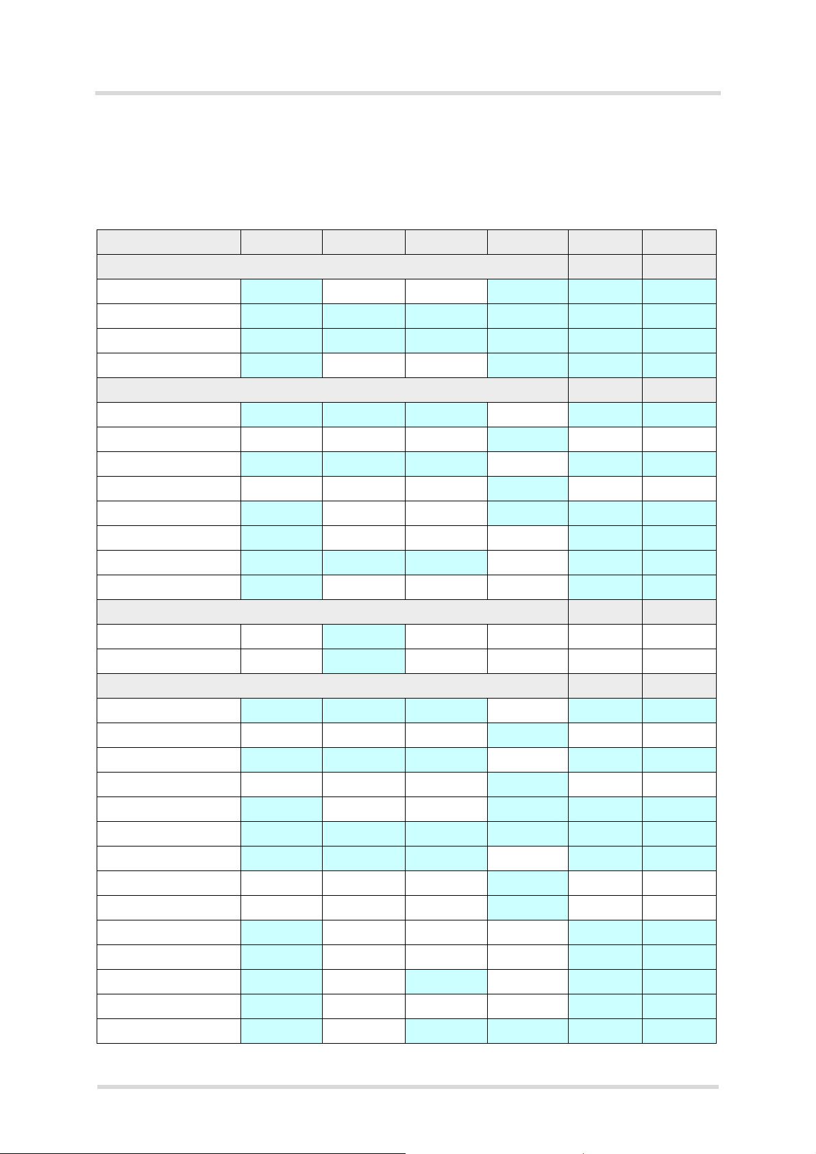
The following table lists the supported frequency bands for each of the ALAS66A product variants mentioned in Section 1.1.
Table 1: Supported frequency bands for each ALAS66A variant
Band -W -CN -E -US -J -K
GSM/GPRS/EDGE
850MHz x x x x
900MHz
1800MHz
1900MHz
UMTS/HSPA
Bd.I (2100MHz) x x x x x
Bd.II (1900MHz)
Bd.III (1800MHz)
Bd.IV (1700MHz)
Bd.V (850MHz)
Bd.VI (850MHz)
Bd.VIII (900MHz)
Bd.XIX (850MHz)
TD-SCDMA
Bd.34 (2000MHz) x
Bd.39 (1900MHz)
LTE-FDD
Bd.1 (2100MHz) x x x x x
1
x x x x x x
x x x x x x
x x x x
x
x x x x x
x
x x x x
x x x
x x x x x
x x x
x
Bd.2 (1900MHz)
Bd.3 (1800MHz)
Bd.4 (1700MHz)
Bd.5 (850MHz)
Bd.7 (2600MHz)
Bd.8 (900MHz)
Bd.12 (700MHz)
Bd.13 (700MHz)
Bd.18 (850MHz)
Bd.19 (850MHz)
Bd.20 (800MHz)
Bd.26 (850MHz)
Bd.28 (700MHz)
ALAS66A_HIO_v01.230/v01.228 2019-07-10
x x x x x
x x x x
x x x x x x
x x x x x
x x x
x x x
x x x x
x x x
x x x x x
Confidential / Released
x
x
x
x
Page 12
Cinterion® ALAS66A Hardware Interface Overview
Page 12 of 51
1.2 Key Features at a Glance
16
Table 1: Supported frequency bands for each ALAS66A variant
Band -W -CN -E -US -J -K
Bd.29 (700MHz)
x
<supplementary
downlink>
Bd.30 (2300MHz)
2
x
<supplementary
downlink only acc.
FCC regulation>
Bd.32 (1500MHz)
x x x x
<supplementary
downlink>
Bd.66 (1700MHz)
LTE-TDD
4
3
x
Bd.34 (2000MHz) x x x x
Bd.38 (2600MHz)
Bd.39 (1900MHz)
Bd.40 (2300MHz)
Bd.41 (2600MHz)
1. Bd.5, Bd.8, Bd.29, and Bd.32 support 2x2 MIMO only, whereas Bd.1, Bd.2, Bd.3, Bd.4, Bd.7, and Bd.66
support 4x4 MIMO in downlink. Also, Bd.2, Bd.3, Bd.4, Bd.5, Bd.8, Bd.12, Bd.13, Bd.18, Bd.19, Bd.20,
Bd.26, Bd.28 support 4 antenna RX Diversity (HoRXD).
2. Band 30 support is disabled by means of software due to AT&T advice.
3. With the Band 66 support, the frequency ranges 1755-1780 MHz and 2155-2180 MHz derived from pairing the 1710-1780 and 2110-2180 MHz frequency bands are compliant with §§27.5(h) and 27.75.
4. Bd.34 supports 2x2 MIMO only, whereas Bd.38, Bd.39, Bd.40, and Bd.41 support 4x4 MIMO in downlink.
5. Note: Out of the 3GPP specified frequency range for LTE Band 41, only that part which is used in China
and Japan (2545MHz to 2655MHz) is supported by ALAS66A. Therefore, support for Band 41 is disabled by means of software in ALAS66A-W and ALAS66A-K variants.
5
x x x x x
x x x x
x x x x
x x x x
1.2.2 Supported CA Configurations
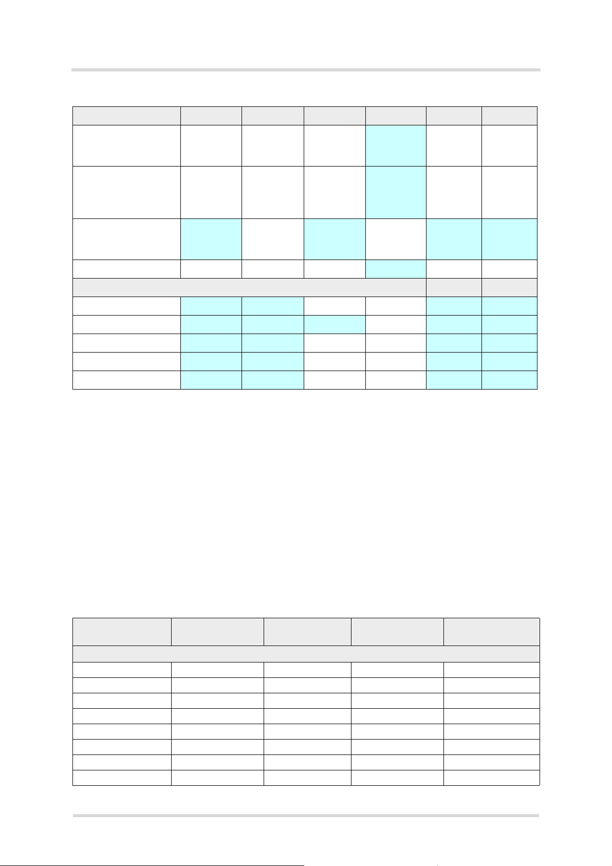
The following table lists the supported CA configurations for each of the ALAS66A product variants mentioned in Section 1.1.
Table 2: Supported CA configurations
Downlink CA Downlink
(4x4 MIMO)
Intra-band continuous
CA_1C 1C - 0,1 E, W, CN, J, K
CA_2C 2C - 0 US
CA_3C 3C CA_3C 0 E, W, CN, J, K
CA_5B - - 0,1 US, W, J, K
CA_7B 7B - 0 E, US, W, CN, J, K
CA_7C 7C CA_7C 0, 1, 2 E, US, W, CN, J, K
CA_8B - - 0 E, W, CN, J, K
CA_12B - - 0 US
ALAS66A_HIO_v01.230/v01.228 2019-07-10
Uplink CA Bandwidth
combination set
Confidential / Released
Product variants
(ALAS66A-...)
Page 13

Cinterion® ALAS66A Hardware Interface Overview
Page 13 of 51
1.2 Key Features at a Glance
16
Table 2: Supported CA configurations
Downlink CA Downlink
(4x4 MIMO)
CA_38C 38C CA_38C 0 E, W, CN, J, K
CA_40C 40C CA_40C 0, 1 W, CN, J, K
CA_40D - - 0,1 W, CN, J, K
CA_41C 41C CA_41C 0,1,2,3 CN, J
CA_41D - CA_41C 0 CN, J
CA_66B 66B - 0 US
CA_66C 66C - 0 US
Uplink CA Bandwidth
combination set
Product variants
(ALAS66A-...)
Intra-band non-continuous
CA_2A-2A 2A-2A - 0 US
CA_4A-4A 4A-4A - 0,1 US
CA_66A-66A 66A-66A - 0 US
Inter-band (two bands)
CA_1A-3A - - 0,1 E, W, CN, J, K
CA_1A-3C - CA_3C 0 E, W, CN, J, K
CA_1A-5A 1A CA_1A-5A 0, 1 W
CA_1A-7A - - 0 E, W, CN, J, K
CA_1A-8A 1A CA_1A-8A 0, 1, 2 E, W, CN, J, K
CA_1A-18A 1A CA_1A-18A 0, 1 W, J, K
CA_1A-19A 1A - 0 W, J, K
CA_1A-20A 1A - 0 E, W, J, K
CA_1A-26A 1A CA_1A-26A 0, 1 W, J, K
CA_1A-28A 1A CA_1A-28A 0, 1 E, W, J, K
CA_2A-2A-4A - - 0 US
CA_2A-2A-4A-4A - - 0 US
CA_2A-2A-5A 2A - 0 US
CA_2A-2A-12A 2A - 0 US
CA_2A-2A-13A 2A - 0 US
CA_2A-2A-66A - - 0 US
CA_2A-4A - - 0, 1, 2 US
CA_2A-4A-4A - - 0 US
CA_2A-5A 2A - 0, 1 US
CA_2A-12A 2A - 0, 1, 2 US
CA_2A-12B 2A - 0 US
CA_2A-13A 2A - 0, 1 US
CA_2A-28A 2A - 0 US
CA_2A-29A 2A - 0, 1, 2 US
CA_2A-66A - - 0,1,2 US
CA_2A-66A-66A - - 0 US
CA_2C-5A 2C - 0 US
CA_2C-12A 2C - 0 US
CA_2C-29A 2C - 0 US
CA_3A-3A-8A 3A CA_7C 0, 1 E, W, CN, J, K
ALAS66A_HIO_v01.230/v01.228 2019-07-10
Confidential / Released
Page 14

Cinterion® ALAS66A Hardware Interface Overview
Page 14 of 51
1.2 Key Features at a Glance
16
Table 2: Supported CA configurations
Downlink CA Downlink
(4x4 MIMO)
CA_3A-5A 3A CA_3A-8A 0, 1, 2, 3,4 W, J, K
CA_3A-7A - - 0, 1 E, W, CN, J, K
CA_3A-7B - CA_3A-20A 0 E, W, CN, J, K
CA_3A-7C - - 0, 1 E, W, CN, J, K
CA_3A-8A 3A - 0, 1, 2, 3 E, W, CN, J, K
CA_3A-19A 3A - 0 W, J, K
CA_3A-20A 3A CA_3C 0, 1 E, W, J, K
CA_3A-26A 3A - 0, 1 W, J, K
CA_3A-28A 3A CA_3A-20A 0,1 E, W, J, K
CA_3C-5A 3C - 0 W, J, K
CA_3C-7A - - 0 E, W, CN, J, K
CA_3C-7C - - 0,1 E, W, J, K
CA_3C-8A - CA_3C-8A, CA_3C 0 W, J, K
CA_3C-20A 3C - 0 E, W, J, K
CA_3C-28A 3C - 0 E, W, J, K
CA_4A-4A-5A 4A - 0 US
CA_4A-4A-7A - - 0, 1 US
CA_4A-4A-12A 4A - 0 US
CA_4A-4A-13A 4A - 0 US
CA_4A-5A 4A - 0, 1 US
CA_4A-7A - - 0, 1 US
CA_4A-12A 4A - 0,1,2,3,4,5 US
CA_4A-12B 4A - 0 US
CA_4A-13A 4A - 0, 1 US
CA_4A-28A - - 0 US
CA_4A-29A 4A - 0, 1, 2 US
CA_5A-7A 7A CA_5A-7A 0, 1 US, W, J, K
CA_5A-12A - - 0 US
CA_5A-66A 66A - 0 US
CA_5A-66A-66A 66A - 0 US
CA_7A-8A 7A - 0, 1,2 E, W, CN, J, K
CA_7A-12A 7A - 0 US
CA_7A-20A 7A CA_7A-20A 0, 1 E, W, J, K
CA_7A-28A 7A - 0, 1 E, US, W, J, K
CA_7B-28A 7B - 0 E, US, W, J, K
CA_7C-28A 7C CA_7C 0 E, US, W, J, K
CA_8A-20A - - 0, 1 E, W, J, K
CA_12A-66A 66A - 0,1,2,3,4,5 US
CA_12A-66A-66A 66A - 0 US
CA_13A-66A 66A - 0 US
CA_13A-66A-66A 66A - 0 US
CA_18A-28A - - 0 W, J, K
Uplink CA Bandwidth
combination set
Product variants
(ALAS66A-...)
ALAS66A_HIO_v01.230/v01.228 2019-07-10
Confidential / Released
Page 15
Cinterion® ALAS66A Hardware Interface Overview
Page 15 of 51
1.2 Key Features at a Glance
16
Table 2: Supported CA configurations
Downlink CA Downlink
(4x4 MIMO)
CA_20A-32A - - 0,1 E, W, J, K
CA_39A-41A - - 0 CN
CA_39A-41C - CA_41C 0 CN
CA_39C-41A - CA_39C 0 CN
Uplink CA Bandwidth
combination set
Product variants
(ALAS66A-...)
Inter-band (three bands)
CA_1A-3A-5A - CA_1A-5A,
CA_3A-5A
CA_1A-3A-8A - CA_1A-8A,
CA_3A-8A
CA_1A-3A-19A - - 0 W, J, K
CA_1A-3A-20A - CA_3A-20A 0 E, W, J, K
CA_1A-3A-26A - - 0 W, J, K
CA_1A-3A-28A - - 0 E, W, J, K
CA_1A-5A-7A - CA_1A-5A,
CA_5A-7A
CA_1A-7A-8A - - 0 E, W, CN, J, K
CA_1A-7A-20A - - 0,1 E, W, J, K
CA_1A-7A-28A - - 0,1,2 E, W, J, K
CA_1A-18A-28A 1A - 0, 1 W, J, K
CA_1A-19A-28A - - 0 W, J, K
CA_2A-2A-4A-12A - - 0 US
CA_2A-2A-12A-66A - - 0 US
CA_2A-4A-4A-12A - - 0 US
CA_2A-4A-5A - - 0 US
CA_2A-4A-12A - - 0 US
CA_2A-4A-13A - - 0 US
CA_2A-4A-29A - - 0 US
CA_2A-5A-66A - - 0 US
CA_2A-12A-66A - - 0 US
CA_2A-12A-66A-66A - - 0 US
CA_2A-13A-66A - - 0 US
CA_3A-7A-8A - CA_3A-8A 0, 1,2 E, W, CN, J, K
CA_3A-7A-28A - - 0 E, W, J, K
CA_3A-7C-28A - - 0 E, W, J, K
CA_4A-7A-12A - - 0, 1 US
0, 1 E, W, J, K
0,1,2,3 E, W, CN, J, K
0, 1 E, W, J, K
ALAS66A_HIO_v01.230/v01.228 2019-07-10
Confidential / Released
Page 16

Cinterion® ALAS66A Hardware Interface Overview
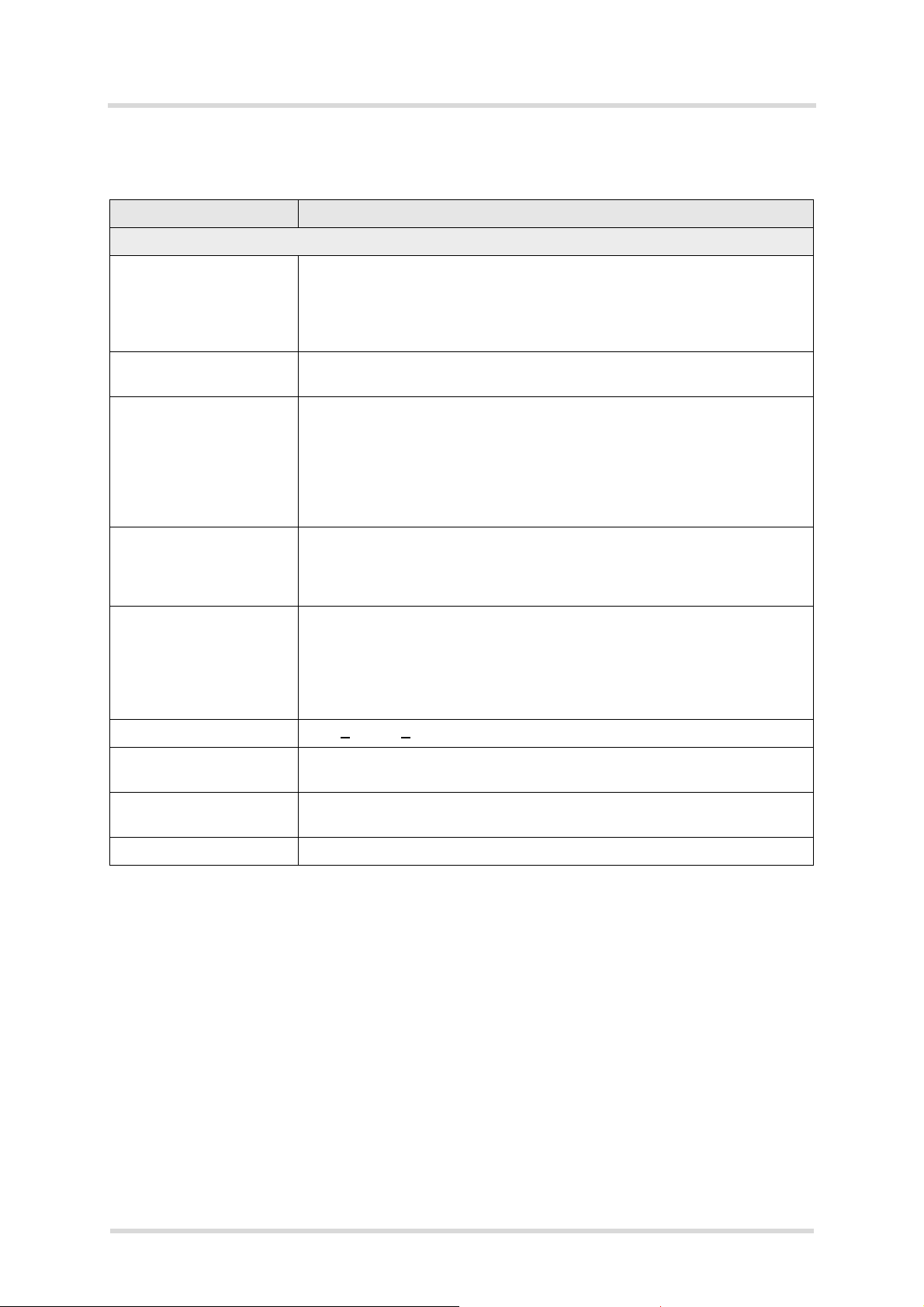
Power
Supply
IGT
EMERG_OF F
Application
Interfaces
ALAS66A
Application
VEXT
PWR_IND
Serial Interface
Digital
Audio
GNSS
Application
USIM
SIM
Card
Codec
GSM/UMTS/LTE
GPIO
Antenna-
diagnostic
4 x
ADC
I2S
I2C
I2C
Serial Interface
I2C
USB
2.0/3.0
ASC0
ASC1
I2C
Digital
Audio
GPIO
I2S
USB
Antenna-
diagnostic
External Antenna
Switch (optional)
TRX1 TRX2 RX3 RX4GNSS
GPIO
Power
Supp ly
eMMC
eMMC Interface
Power
Supply
PCIe
PCIe
3 x
ANT _SW
1.3 System Overview
16
1.3 System Overview
Page 16 of 51
Figure 1: ALAS66A system overview
ALAS66A_HIO_v01.230/v01.228 2019-07-10
Confidential / Released
Page 17

Cinterion® ALAS66A Hardware Interface Overview
BATT+
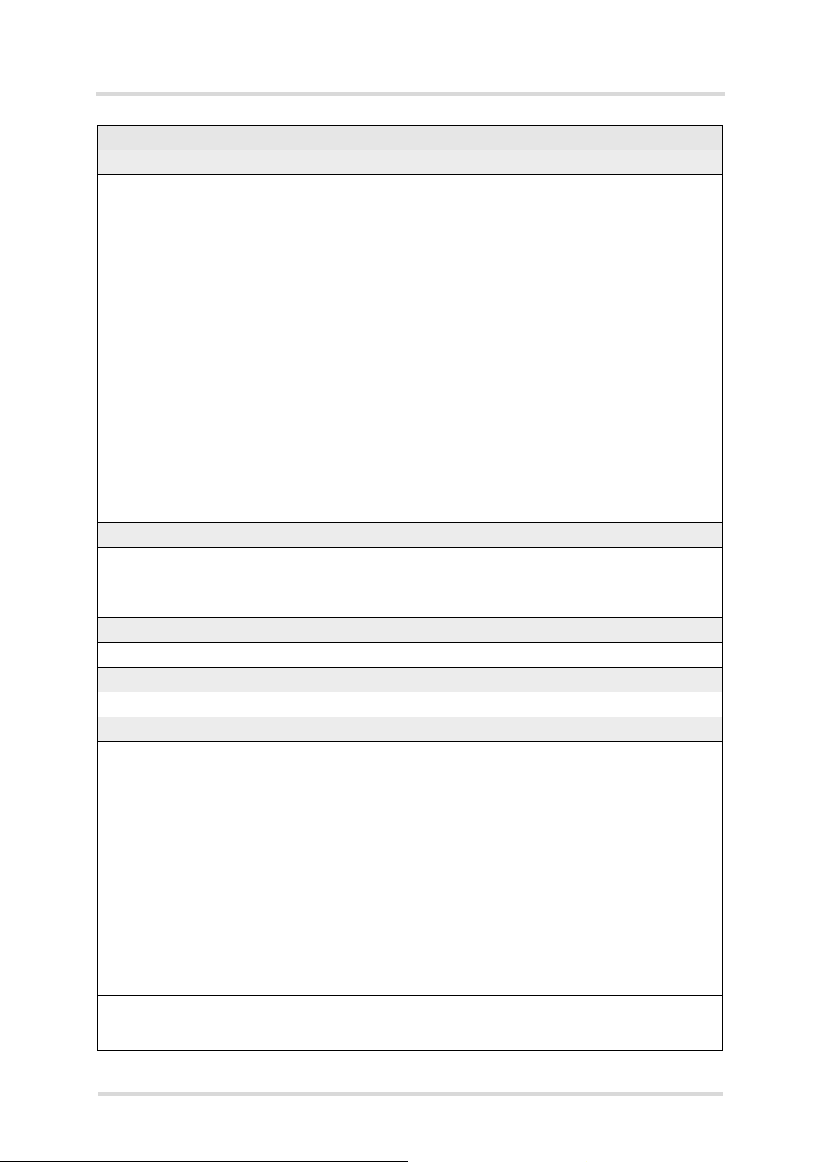
USB_DP
c)
lin. reg.
GND
Module
Detection only
VUSB_IN
b)
USB part
a)
a)
All serial (including RS) and pull -up resistors for data lines are implemented .
USB_DN
c)
c)
If the USB interface is operated with super or high speeds, it is recommended to take special care routing the data
lines. Application layout should implement a differential impedance of 90 ohms for proper signal integrity .
VBUS
1µF
b)
Since VUSB_IN is used for detection only it is recommended not to add any further blocking capacitors on
the VUSB_IN line.
USB_SSRX_N
c)
USB_SSRX_P
c)
USB_SSTX_N
c)
USB_SSTX_P
c)
USB_SS
_PHY
USB_HS
_PHY
USB 2.0
Controller
USB 3.0
Controller
2.0
2.0
3.0
100nF
100nF
SMT
Page 17 of 51
2 Interface Characteristics
33
2 Interface Characteristics
ALAS66A is equipped with an SMT application interface that connects to the external application. The SMT application interface incorporates the various application interfaces as well as
the RF antenna interface.
2.1 Application Interface
2.1.1 USB Interface
ALAS66A supports a USB 3.0 Super Speed (5Gbps) device interface, and alternatively a USB
2.0 device interface that is High Speed compatible. The USB interface is primarily intended for
use as debugging interface.
The USB host is responsible for supplying the VUSB_IN line. This line is for voltage detection
only. The USB part (driver and transceiver) is supplied by means of BATT+. This is because
ALAS66A is designed as a self-powered device compliant with the “Universal Serial Bus Specification Revision 3.0”
1
.
To properly connect the module's USB interface to the external application, a USB 3.0 or 2.0
Figure 2: USB circuit
compatible connector and cable or hardware design is required. Furthermore, the USB driver
distributed with ALAS66A needs to be installed.
1. The specification is ready for download on http://www.usb.org/developers/docs/
ALAS66A_HIO_v01.230/v01.228 2019-07-10
Confidential / Released
Page 18

Cinterion® ALAS66A Hardware Interface Overview
2.1 Application Interface
33
Page 18 of 51
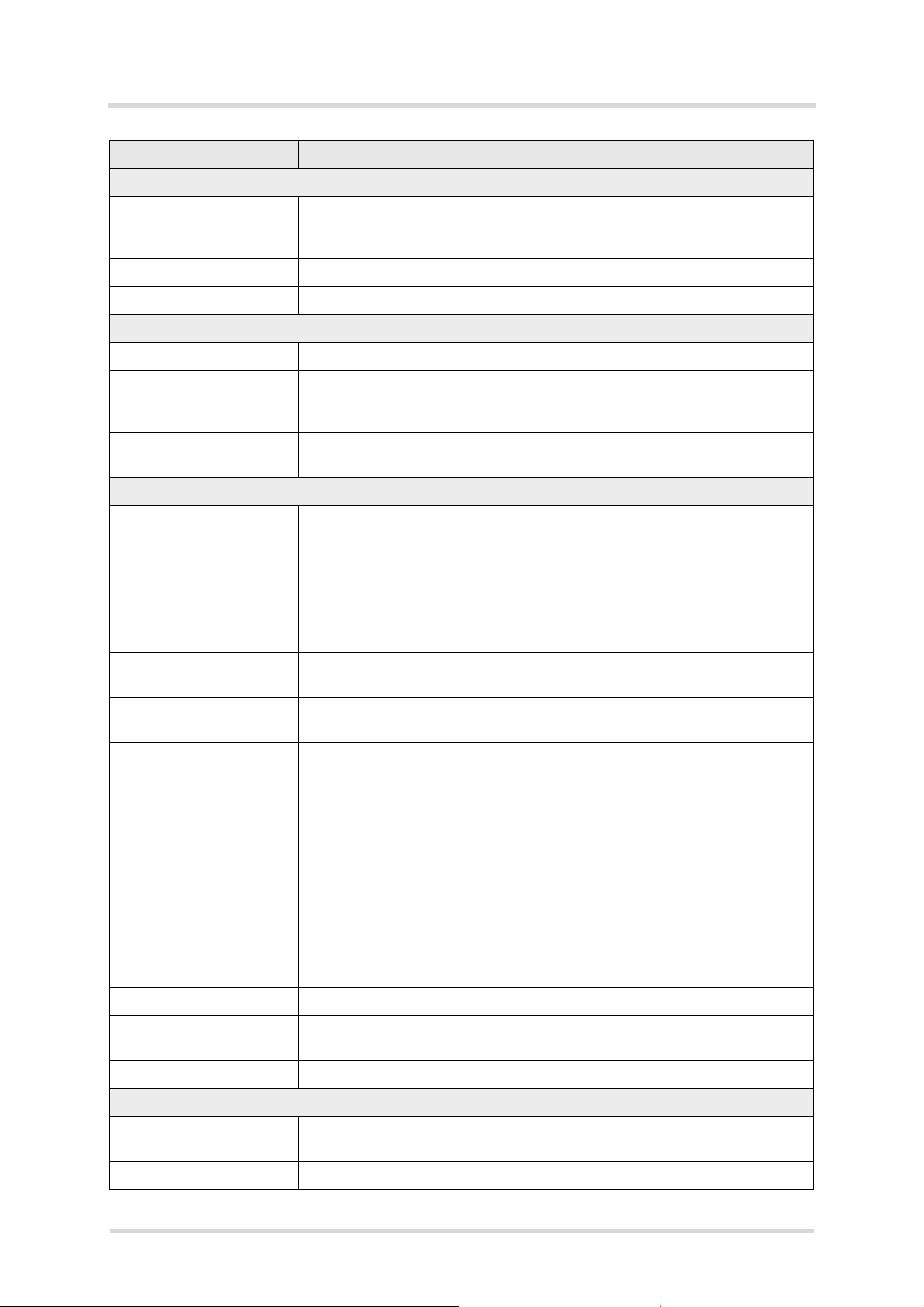
2.1.2 Serial Interface ASC0
ALAS66A offers a 4-wire (8-wire prepared) (plus GND) unbalanced, asynchronous interface
ASC0 conforming to ITU-T V.24 protocol DCE signaling. The electrical characteristics do not
comply with ITU-T V.28. The significant levels are 0V (for low data bit or active state) and 1.8V
(for high data bit or inactive state).
ALAS66A is designed for use as a DCE. Based on the conventions for DCE-DTE connections
it communicates with the customer application (DTE) using the following signals:
• Port TXD @ application sends data to the module’s TXD0 signal line
• Port RXD @ application receives data from the module’s RXD0 signal line
Figure 3: Serial interface ASC0
Features:
• Includes the data lines TXD0 and RXD0, the status lines RTS0 and CTS0. The modem control lines DTR0, DSR0, DCD0 and RING0 are not yet implemented.
• The RING0 signal serves to indicate incoming calls and other types of URCs (Unsolicited
Result Code). It can also be used to send pulses to the host application, for example to
wake up the application from power saving state. Not yet implemented.
• Configured for 8 data bits, no parity and 1 stop bit.
• ASC0 can be operated at fixed bit rates from 115,200 to 921,600bps.
• Supports RTS0/CTS0 hardware flow control.
Note: If the ASC0 serial interface is the application’s only interface, it is suggested to connect
test points on the USB signal lines as a potential tracing possibility.
ALAS66A_HIO_v01.230/v01.228 2019-07-10
Confidential / Released
Page 19

Cinterion® ALAS66A Hardware Interface Overview
2.1 Application Interface
33
Page 19 of 51
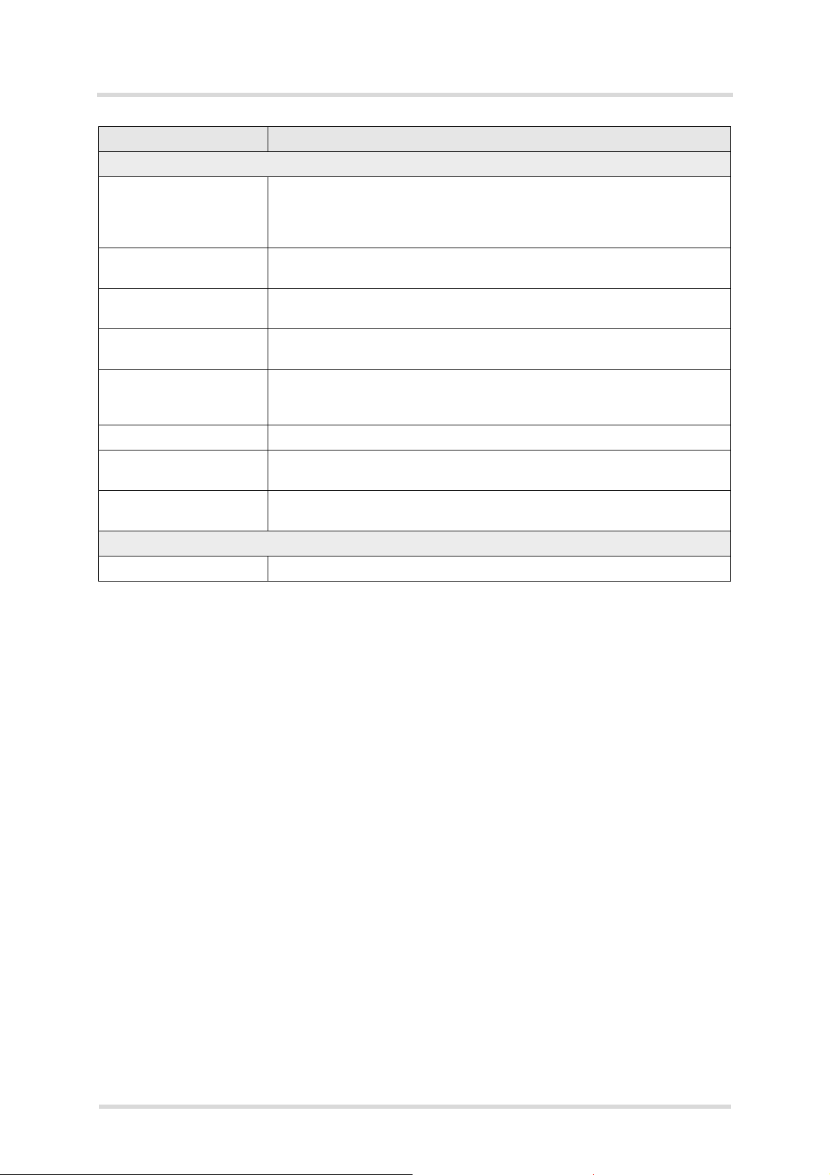
2.1.3 Serial Interface ASC1
Four ALAS66A lines can be configured as ASC1 interface signals to provide a 4-wire unbalanced, asynchronous interface ASC1 conforming to ITU-T V.24 protocol DCE signaling. The
electrical characteristics do not comply with ITU-T V.28. The significant levels are 0V (for low
data bit or active state) and 1.8V (for high data bit or inactive state).
ALAS66A is designed for use as a DCE. Based on the conventions for DCE-DTE connections
it communicates with the customer application (DTE) using the following signals:
• Port TXD @ application sends data to module’s TXD1 signal line
• Port RXD @ application receives data from the module’s RXD1 signal line
Figure 4: Serial interface ASC1
Features
• Includes only the data lines TXD1 and RXD1 plus RTS1 and CTS1 for hardware handshake.
• On ASC1 no RING line is available.
• Configured for 8 data bits, no parity and 1 or 2 stop bits.
• ASC1 can be operated at fixed bit rates from 115,200 bps to 921,600 bps.
• Supports RTS1/CTS1 hardware flow.
ALAS66A_HIO_v01.230/v01.228 2019-07-10
Confidential / Released
Page 20

Cinterion® ALAS66A Hardware Interface Overview
I2CCLK
I2CDAT
GND
I2CCLK
I2CDAT
GND
Module Application
VEXT
R pull up
R pull up
Page 20 of 51
2.1 Application Interface
33
2.1.4 I2C Interface
ALAS66A provides two I2C interfaces. I2C is a serial, 8-bit oriented data transfer bus for bit rates
up to 400kbps in Fast mode. It consists of two lines, the serial data line I2CDAT and the serial
clock line I2CCLK. The module acts as a single master device, e.g. the clock I2CCLK is driven
by the module. I2CDAT is a bi-directional line. Each device connected to the bus is software
addressable by a unique 7-bit address, and simple master/slave relationships exist at all times.
The module operates as master-transmitter or as master-receiver. The customer application
transmits or receives data only on request of the module.
The applications I
the VEXT line, the I
2
C interface can be powered via the VEXT line of ALAS66A. If connected to
2
C interface will properly shut down when the module enters the Power
Down mode.
In the application I2CDATx and I2CCLKx lines need to be connected to a positive supply voltage (e.g., VEXT) via a pull-up resistor.
Figure 5: I2C interface connected to VEXT
Note: Good care should be taken when creating the PCB layout of the host application: The
traces of I2CCLK and I2CDAT should be equal in length and as short as possible.
ALAS66A_HIO_v01.230/v01.228 2019-07-10
Confidential / Released
Page 21

Cinterion® ALAS66A Hardware Interface Overview
2.1 Application Interface
33
Page 21 of 51
2.1.5 UICC/SIM/USIM Interface
ALAS66A has a UICC/SIM/USIM interface compatible with the 3GPP 31.102 and ETSI 102
221. It is wired to the host interface in order to be connected to an external SIM card holder.
Five pads on the SMT application interface are reserved for the SIM interface.
The UICC/SIM/USIM interface supports 2.85V and 1.8V SIM cards.
The CCIN signal serves to detect whether a tray (with SIM card) is present in the card holder.
Using the CCIN signal is mandatory for compliance with the GSM 11.11 recommendation if the
mechanical design of the host application allows the user to remove the SIM card during operation. To take advantage of this feature, an appropriate SIM card detect switch is required on
the card holder. For example, this is true for the model supplied by Molex, which has been tested to operate with ALAS66A and is part of the Gemalto M2M reference equipment submitted
for type approval. See Chapter 7 for Molex ordering numbers.
Table 3: Signals of the SIM interface (SMT application interface)
Signal Description
GND Ground connection for SIM interfaces. Optionally a separate SIM ground line may be used
to improve EMC.
CCCLK Chipcard clock line for SIM interface.
CCVCC SIM supply voltage line for SIM interface.
CCIO Serial data line for SIM interface, input and output.
CCRST Chipcard reset line SIM interface.
CCIN Input on the baseband processor for detecting a SIM card tray in the holder. If the SIM is
removed during operation the SIM interface is shut down immediately to prevent destruction of the SIM. The CCIN signal is active low.
The CCIN signal is mandatory for applications that allow the user to remove the SIM card
during operation.
The CCIN signal is solely intended for use with a SIM card. It must not be used for any other
purposes. Failure to comply with this requirement may invalidate the type approval of
ALAS66A.
Note: No guarantee can be given, nor any liability accepted, if loss of data is encountered after
removing the SIM card during operation. Also, no guarantee can be given for properly initializing any SIM card that the user inserts after having removed the SIM card during operation. In
this case, the application must restart ALAS66A.
ALAS66A_HIO_v01.230/v01.228 2019-07-10
Confidential / Released
Page 22

Cinterion® ALAS66A Hardware Interface Overview
Module
open: Card removed
closed: Card inserted
CCRST
CCVCC
CCIO
CCCLK
CCIN
SIM /
UICC
1n
220n
SMT application interface
GND
2.1 Application Interface
33
Figure 6: First UICC/SIM/USIM interface
Page 22 of 51
The total cable length between the SMT application interface pads on ALAS66A and the pads
of the external SIM card holder must not exceed 100mm in order to meet the specifications of
3GPP TS 51.010-1 and to satisfy the requirements of EMC compliance.
To avoid possible cross-talk from the CCCLK signal to the CCIO signal be careful that both
lines are not placed closely next to each other. A useful approach is using the GND line to
shield the CCIO line from the CCCLK line.
ALAS66A_HIO_v01.230/v01.228 2019-07-10
Confidential / Released
Page 23

Cinterion® ALAS66A Hardware Interface Overview
2.1 Application Interface
33
Page 23 of 51
2.1.6 Digital Audio Interface
ALAS66A supports one digital audio interface that can be employed as inter IC sound (I2S) interface.
2.1.6.1 Inter IC Sound Interface (I2S)
The I2S Interface is a standardized bidirectional I2S ("Inter-IC Sound Interface") based digital
audio interface for transmission of mono voice signals for telephony services.
2
The I
S properties and capabilities comply with the requirements layed out in the Phillips I2S
Bus Specifications, revised June 5, 1996.
2.1.7 Analog-to-Digital Converter (ADC)
ALAS66A provides four unbalanced ADC input lines: ADC[1-2...4-5]_IN. They can be used to
measure four independent, externally connected DC voltages in the range of 0.1V to 1.7V.
2.1.8 GPIO Interface
ALAS66A has 18 GPIOs for external hardware devices. Each GPIO can be configured for use
as input or output.
2.1.9 eMMC Interface
ALAS66A has an eMMC interface that can be used for test purposes, e.g., to write crash dumps
from the module’s FFS to eMMC.
ALAS66A_HIO_v01.230/v01.228 2019-07-10
Confidential / Released
Page 24

Cinterion® ALAS66A Hardware Interface Overview
2.2 GSM/UMTS/LTE Antenna Interface
33
Page 24 of 51
2.2 GSM/UMTS/LTE Antenna Interface
The ALAS66A GSM/UMTS/LTE antenna interface comprises two GSM/UMTS/LTE main antennas as well as two UMTS/LTE Rx diversity/MIMO antennas to improve signal reliability and
quality
match at the antenna interface without any damage, even when transmitting at maximum RF
power.
The external antennas must be matched properly to achieve best performance regarding radiated power, modulation accuracy and harmonic suppression. Matching networks are not included on the ALAS66A PCB and should be placed in the host application, if the antenna does
not have an impedance of 50
Regarding the return loss ALAS66A provides the following values in the active band:
Table 4: Return loss in the active band
1
. The interface has an impedance of 50. ALAS66A is capable of sustaining a total mis-
.
State of module Return loss of module Recommended return loss of application
Receive >
Transmit Undefined mismatch >
8dB > 12dB
12dB
1. By delivery default the UMTS/LTE Rx diversity/MIMO antennas are configured as available for the module since its usage is mandatory for LTE. Please refer to [1] for details on how to configure antenna settings.
ALAS66A_HIO_v01.230/v01.228 2019-07-10
Confidential / Released
Page 25

Cinterion® ALAS66A Hardware Interface Overview
2.2 GSM/UMTS/LTE Antenna Interface
33
Page 25 of 51
2.2.1 Antenna Installation
The antennas are connected by soldering the antenna pads (ANT_TRX1, ANT_TRX2,
ANT_RX3, ANT_RX4; ANT_GNSS) and their neighboring ground pads directly to the application’s PCB.
The distance between the antenna pads and their neighboring GND pads has been optimized
for best possible impedance. To prevent mismatch, special attention should be paid to these
pads on the application’ PCB.
The wiring of the antenna connection, starting from the antenna pad to the application’s antenna must result in a 50
optimized with regard to the PCB’s layer stack.
To prevent receiver desensitization due to interferences generated by fast transients like high
speed clocks on the external application PCB, it is recommended to realize the antenna connection line using embedded Stripline rather than Micro-Stripline technology. Please see Sec-
tion 2.2.2 for instructions of how to design the antenna connection in order to achieve the
required 50
line impedance.
line impedance. Line width and distance to the GND plane need to be
For type approval purposes(i.e., FCC KDB 996369 related to modular approval requirements),
an external application must connect the RF signal in one of the following ways:
•Via 50
coaxial antenna connector (common connectors are U-FL or SMA) placed as close
as possible to the module's antenna pad.
• By soldering the antenna to the antenna connection line on the application’s PCB (without
the use of any connector) as close as possible to the module’s antenna pad.
• By routing the application PCB’s antenna to the module’s antenna pad in the shortest possible way.
ALAS66A_HIO_v01.230/v01.228 2019-07-10
Confidential / Released
Page 26

Cinterion® ALAS66A Hardware Interface Overview
2.2 GSM/UMTS/LTE Antenna Interface
33
Page 26 of 51
2.2.2 RF Line Routing Design
2.2.2.1 Line Arrangement Instructions
Several dedicated tools are available to calculate line arrangements for specific applications
and PCB materials - for example from http://www.polarinstruments.com/ (commercial software)
or from http://web.awrcorp.com/Usa/Products/Optional-Products/TX-Line/ (free software).
Embedded Stripline
This below figure shows line arrangement examples for embedded stripline.
Figure 7: Embedded Stripline line arrangement
ALAS66A_HIO_v01.230/v01.228 2019-07-10
Confidential / Released
Page 27

Cinterion® ALAS66A Hardware Interface Overview
2.2 GSM/UMTS/LTE Antenna Interface
33
Micro-Stripline
This section gives two line arrangement examples for micro-stripline.
Page 27 of 51
Figure 8: Micro-Stripline line arrangement samples
ALAS66A_HIO_v01.230/v01.228 2019-07-10
Confidential / Released
Page 28

Cinterion® ALAS66A Hardware Interface Overview
G N D
G N D
Edge of m odule PCB
Stripline (50 ohms) on top
layer of evaluation board from
antenna pad to module edge
Width = 0.50 mm
E.g., U.FL antenna
connector
50 ohms microstrip line
G N D G N D
Ground connection
e.g.
ANT_
TRX1
RF track under module:
Line/space: 500/350μm
RF track outside module:
Line/space:
750/300μm
Module ĞĚŐĞ
Page 28 of 51
2.2 GSM/UMTS/LTE Antenna Interface
33
2.2.2.2 Routing Examples
Interface to RF Connector
Figure 9 and Figure 10 show a sample connection of a module‘s antenna pad at the bottom
layer of the module PCB with an application PCB‘s coaxial antenna connector. Line impedance
depends on line width, but also on other PCB characteristics like dielectric, height and layer
gap. The sample stripline width of 0.50mm/0.75mm and the spaces of 0.35mm/0.3mm are only
recommended for an application with a PCB layer stack resembling the one of the ALAS66A
evaluation board, and with layer 2 as well as layer 3 cut clear. For different layer stacks the
stripline width will have to follow stripline routing rules, avoiding 90 degree corners and using
the shortest distance to the PCB’s coaxial antenna connector.
ALAS66A_HIO_v01.230/v01.228 2019-07-10
Figure 9: Routing to application‘s RF connector
Figure 10: Routing detail
Confidential / Released
Page 29

Cinterion® ALAS66A Hardware Interface Overview
V
GNSS
Active GNSS
Antenna
DC
+
-
Current Sensor
FAN4010
Is
Rs
(3.2V)
Io
Rv
Io
ADCx_ IN
Rg
Ug
GNSS
Receiver
Antenna
Matching
RF
DC
ANT _GNSS_ DC
ANT_GNSS
Module
Application:
3k3
1u
10k
ESD
Protection
LNA
100
1R0
LDO
BATT +
EN
IN OUT
GNSS_EN
LP3985IM5-3.2
10k
Si1023X_1
Si1023X_2
Page 29 of 51
2.3 GNSS Antenna Interface
33
2.3 GNSS Antenna Interface
In addition to the RF antenna interface ALAS66A also has a GNSS antenna interface. The
GNSS pad’s shape is the same as for the RF antenna interface (see Section 2.2.1).
It is possible to connect active or passive GNSS antennas. In either case they must have 50
impedance. The simultaneous operation of GSM/UMTS/LTE and GNSS is implemented.
ALAS66A provides the signal GNSS_EN to enable an active GNSS antenna power supply. Fig-
ure 11 shows the flexibility in realizing the power supply for an active GNSS antenna by giving
a sample circuit realizing the supply voltage for an active GNSS antenna.
Figure 11: Supply voltage for active GNSS antenna
ALAS66A_HIO_v01.230/v01.228 2019-07-10
Confidential / Released
Page 30

Cinterion® ALAS66A Hardware Interface Overview
GNSS_EN
ANT_ GNSS
Passive
GNSS
antenna
10nH
100nF
To GNSS
receiver
Module
SMT interface
ANT_ GNSS _DC
(Optional)
ESD
protection
0R
Not used
Page 30 of 51
2.3 GNSS Antenna Interface
33
Figure 12 shows a sample circuit realizing ESD protection for a passive GNSS antenna. Con-
necting the input ANT_GNSS_DC to GND prevents ESD from coupling into the module.
Figure 12: ESD protection for passive GNSS antenna
ALAS66A_HIO_v01.230/v01.228 2019-07-10
Confidential / Released
Page 31

Cinterion® ALAS66A Hardware Interface Overview
2.4 Sample Application
33
Page 31 of 51
2.4 Sample Application
Figure 13 shows a typical example of how to integrate an ALAS66A module with an application.
The PWR_IND line is an open collector that needs an external pull-up resistor which connects
to the voltage supply VCC µC of the microcontroller. Low state of the open collector pulls the
PWR_IND signal low and indicates that the ALAS66A module is active, high level notifies the
Power Down mode.
If the module is in Power Down mode avoid current flowing from any other source into the module circuit, for example reverse current from high state external control lines. Therefore, the
controlling application must be designed to prevent reverse flow.
While developing SMT applications it is strongly recommended to provide test points
for certain signals, i.e., lines to and from the module - for debug and/or test purposes.
The SMT application should allow for an easy access to these signals. For details on
how to implement test points see [2].
The EMC measures are best practice recommendations. In fact, an adequate EMC strategy for
an individual application is very much determined by the overall layout and, especially, the position of components.
Some LGA pads are connected to clocks or high speed data streams that might interfere with
the module’s antenna. The RF receiver would then be blocked at certain frequencies (self interference). The external application’s PCB tracks connected to these pads should therefore
be well shielded or kept away from the antenna. This applies especially to the USB and UICC/
SIM interfaces.
Depending on the micro controller used by an external application ALAS66A‘s digital input and
output lines may require level conversion.
Disclaimer:
No warranty, either stated or implied, is provided on the sample schematic diagram shown in
Figure 13 and the information detailed in this section. As functionality and compliance with na-
tional regulations depend to a great amount on the used electronic components and the individual application layout manufacturers are required to ensure adequate design and operating
safeguards for their products using ALAS66A modules.
ALAS66A_HIO_v01.230/v01.228 2019-07-10
Confidential / Released
Page 32

Cinterion® ALAS66A Hardware Interface Overview
USB_DP, USB_DN
CCVCC
CCRST
CCCLK
CCIN
CCIO
SIM
220nF
1nF
GND
GND
GND
ANT_TRX1
BATT+
GSM/UMTS/LTE
Module
All SIM components should be
close to car d holder. Keep SIM
wires low capac itive.
BATT +_RF
USB_SS...
47µF Ultra low ESR
GND
GND
ANT_TRX2
GSM/UMTS/LTE
EMERG _OF F
47k
IGT
47k
2
2
4 x 47µF
Ultra low ESR
NTC
+
Rechargeable
Lithium battery
Optio nal low
capacitanc e ESD
protection **
VUSB _IN
USB 2.0 HS
Mode
Or
USB 3 .0 SS
Mode
4
2
PCM 2_...
4
PCM interface lines
4
Level
Controller
VDD
(1.8 V)
VCC µC
V
CCA
V
CCB
OE
VEXT ( 1.8V )
PWR _IND
100k
VCC µC
GND
GND
ANT _RX3
UMTS/LTE
GND
GND
ANT _RX4
UMTS/LTE
GND
GND
ANT_ GNSS
GNSS
RXD0, TXD0, ...
Serial interface
ASC0
8
2.4 Sample Application
33
Page 32 of 51
Figure 13: ALAS66A sample application
ALAS66A_HIO_v01.230/v01.228 2019-07-10
Confidential / Released
Page 33

Cinterion® ALAS66A Hardware Interface Overview
3 GNSS Interface
33
Page 33 of 51
3 GNSS Interface
ALAS66A integrates a GNSS receiver that offers the full performance of GPS/GLONASS technology. The GNSS receiver is able to continuously track all satellites in view, thus providing accurate satellite position data.
The integrated GNSS receiver supports the NMEA protocol via USB or ASC0 interface. NMEA
is a combined electrical and data specification for communication between various (marine)
electronic devices including GNSS receivers. It has been defined and controlled by the US
based National Marine Electronics Association. For more information on the NMEA Standard
please refer to http://www.nmea.org.
Depending on the receiver’s knowledge of last position, current time and ephemeris data, the
receiver’s startup time (i.e., TTFF = Time-To-First-Fix) may vary: If the receiver has no knowledge of its last position or time, a startup takes considerably longer than if the receiver has still
knowledge of its last position, time and almanac or has still access to valid ephemeris data and
the precise time.
By default, the GNSS receiver is switched off. It has to be switched on and configured.
Dead Reckoning Sync Line:
Dead reckoning solutions are used in (automotive) platforms to determine the (vehicles) location even when there is no GNSS signal available (e.g. in tunnels, basement garages or even
between high buildings in cities).
In addition to dead reckoning related NMEA sentences, ALAS66A provides a dead reckoning
synchronization line (DR_SYNC line) to be employed in external dead reckoning applications.
DR_SYNC is derived from the GNSS signal clock as 1 pulse per second (1PPS) signal. The
DR_SYNC signal is provided as long as synchronized with the GNSS satellite clock, and continues after GNSS signal loss.
ALAS66A_HIO_v01.230/v01.228 2019-07-10
Confidential / Released
Page 34

Cinterion® ALAS66A Hardware Interface Overview
Top view
Bottom view
4 Mechanical Dimensions and Mounting
35
4 Mechanical Dimensions and Mounting
4.1 Mechanical Dimensions of ALAS66A
Page 34 of 51
Figure 14 shows a 3D view1 of ALAS66A and provides an overview of the board's mechanical
dimensions
Length: 48mm
Width: 36mm
Height: 3mm
2
. For further details see Figure 15.
Figure 14: ALAS66A – top and bottom view
1. The coloring of the 3D view does not reflect the module’s real color.
2. Note: The holes in the shielding (top view) are significantly smaller than the radiated wavelength from
the module. Gemalto guarantees that there will be no emissions outside the limits from these. The RF
circuitry of the module is fully shielded.
ALAS66A_HIO_v01.230/v01.228 2019-07-10
Confidential / Released
Page 35

Cinterion® ALAS66A Hardware Interface Overview
#
#
Öń
#
×ń
Þń
Ûń
ń
ń
ń æńĸń
Nń
ń
ĜĖ
MMĹs!
v ØEĠń çÏ
7
nńńnń5ń5ń
ńń
áń ĺń
Òń
ń
&
ń ń
ń ń ń
#
Õń ńĵ&&&Ļń ń
Ëń
Ķ
oń
!!
Ðń ń ÆF·FÅ ¼
ń ń
ńń
Ī
4
ğ
w
pń
9ń
Äń
ļń
ńńńńńń7?ńńńńńńńńń
Ľń
½ń
ńńħÑń ?7?ń ńńńń
Àń
®ľ
ńń
ń
¸ń tń
9ń
ń
9ń
Ŀ""""x±ń
E
Ô
čńķńÌ~ń
%ń
ń ńćńń £ń ¥ń
è
ŀń
Kńń 6ń ńrń¡ń ń¦ń §ń¨ń6Kń 6ń
Ł
y
5ń
4.1 Mechanical Dimensions of ALAS66A
35
Page 35 of 51
ALAS66A_HIO_v01.230/v01.228 2019-07-10
Figure 15: Dimensions of ALAS66A (all dimensions in mm)
Confidential / Released
Page 36

Cinterion® ALAS66A Hardware Interface Overview
Page 36 of 51
5 Regulatory and Type Approval Information
43
5 Regulatory and Type Approval Information
5.1 Directives and Standards
ALAS66A has been designed to comply with the directives and standards listed below.
It is the responsibility of the application manufacturer to ensure compliance of the final product
with all provisions of the applicable directives and standards as well as with the technical specifications provided in the "ALAS66A Hardware Interface Description".
Table 5: Directives
2014/53/EU Directive of the European Parliament and of the council of 16 April 2014 on
the harmonization of the laws of the Member States relating to the making
available on the market of radio equipment and repealing Directive 1999/
05/EC.
The product is labeled with the CE conformity mark.
1
2002/95/EC (RoHS 1)
2011/65/EC (RoHS 2)
Directive of the European Parliament and of the Council of
27 January 2003 (and revised on 8 June 2011) on the
restriction of the use of certain hazardous substances in
electrical and electronic equipment (RoHS)
Table 6: Standards of North American type approval1
CFR Title 47 Code of Federal Regulations, Part 22, Part 24, Part 27, and Part 90; US
Equipment Authorization FCC
OET Bulletin 65
(Edition 97-01)
Evaluating Compliance with FCC Guidelines for Human Exposure to
Radiofrequency Electromagnetic Fields
UL 60 950-1 Product Safety Certification (Safety requirements)
NAPRD.03 V5.35
2
Overview of PCS Type certification review board Mobile Equipment Type
Certification and IMEI control
PCS Type Certification Review board (PTCRB)
RSS132, RSS133,
Canadian Standard
RSS139
1. Standards apply to ALAS66A-W and ALAS66A-US only.
2. ALAS66A-US complies with NAPRD.03 V5.38.
Table 7: Standards of European type approval
3GPP TS 51.010-1 Digital cellular telecommunications system (Release 7); Mobile Station
(MS) conformance specification;
ETSI EN 301 511
V12.5.1
Global System for Mobile communications (GSM); Mobile Stations (MS)
equipment; Harmonized Standard covering the essential requirements of
article 3.2 of Directive 2014/53/EU
GCF-CC V3.70
1. Manufacturers of applications which can be used in the US shall ensure that their applications have a
PTCRB approval. For this purpose they can refer to the PTCRB approval of the respective module.
1
Global Certification Forum - Certification Criteria
ALAS66A_HIO_v01.230/v01.228 2019-07-10
Confidential / Released
Page 37

Cinterion® ALAS66A Hardware Interface Overview
5.1 Directives and Standards
43
Table 7: Standards of European type approval
Page 37 of 51
ETSI EN 301 489-01
V2.1.1
Draft ETSI EN 301 489-19
V2.1.0
Draft ETSI EN 301 489-52
V1.1.0
ETSI EN 301 908-01
V11.1.1
ETSI EN 301 908-02
V11.1.2
ETSI EN 301 908-13
V11.1.2
Electromagnetic Compatibility (EMC) standard for radio equipment and services; Part 1: Common technical requirements; Harmonized Standard covering the essential requirements of article 3.1(b) of Directive 2014/53/EU
and the essential requirements of article 6 of Directive 2014/30/EU
Electromagnetic Compatibility (EMC) standard for radio equipment and services; Part 19: Specific conditions for Receive Only Mobile Earth Stations
(ROMES) operating in the 1,5 GHz band providing data communications
and GNSS receivers operating in the RNSS band (ROGNSS) providing
positioning, navigation, and timing data; Harmonized Standard covering the
essential requirements of article 3.1(b) of Directive 2014/53/EU
Electromagnetic Compatibility (EMC) standard for radio equipment and services; Part 52: Specific conditions for Cellular Communication Mobile and
portable (UE) radio and ancillary equipment; Harmonized Standard covering the essential requirements of article 3.1(b) of Directive 2014/53/EU
IMT cellular networks; Harmonized Standard covering the essential requirements of article 3.2 of the Directive 2014/53/EU; Part 1: Introduction and
common requirements
IMT cellular networks; Harmonized Standard covering the essential requirements of article 3.2 of the Directive 2014/53/EU; Part 2: CDMA Direct
Spread (UTRA FDD) User Equipment (UE)
IMT cellular networks; Harmonized Standard covering the essential requirements of article 3.2 of the Directive 2014/53/EU; Part 13: Evolved Universal
Terrestrial Radio Access (E-UTRA) User Equipment (UE)
EN 60950-1:2006/
Safety of information technology equipment
A11:2009+A1:2010+A1
2:2011+A2:2013
1. ALAS66A-US complies with GCF-CC V3.72.
Table 8: Requirements of quality
IEC 60068 Environmental testing
DIN EN 60529 IP codes
Table 9: Standards of the Ministry of Information Industry of the People’s Republic of China
SJ/T 11363-2006 “Requirements for Concentration Limits for Certain Hazardous Substances
in Electronic Information Products” (2006-06).
SJ/T 11364-2006 “Marking for Control of Pollution Caused by Electronic
Information Products” (2006-06).
According to the “Chinese Administration on the Control of
Pollution caused by Electronic Information Products”
(ACPEIP) the EPUP, i.e., Environmental Protection Use
Period, of this product is 20 years as per the symbol
shown here, unless otherwise marked. The EPUP is valid only as long as
the product is operated within the operating limits described in the Hardware
Interface Description.
Please see Table 10 for an overview of toxic or hazardous substances or
elements that might be contained in product parts in concentrations above
the limits defined by SJ/T 11363-2006.
ALAS66A_HIO_v01.230/v01.228 2019-07-10
Confidential / Released
Page 38

Cinterion® ALAS66A Hardware Interface Overview
5.1 Directives and Standards
43
Table 10: Toxic or hazardous substances or elements with defined concentration limits
Page 38 of 51
ALAS66A_HIO_v01.230/v01.228 2019-07-10
Confidential / Released
Page 39

Cinterion® ALAS66A Hardware Interface Overview
5.2 SAR requirements specific to portable mobiles
43
Page 39 of 51
5.2 SAR requirements specific to portable mobiles
Mobile phones, PDAs or other portable transmitters and receivers incorporating a GSM module
must be in accordance with the guidelines for human exposure to radio frequency energy. This
requires the Specific Absorption Rate (SAR) of portable ALAS66A based applications to be
evaluated and approved for compliance with national and/or international regulations.
Since the SAR value varies significantly with the individual product design manufacturers are
advised to submit their product for approval if designed for portable use. For US and European
markets the relevant directives are mentioned below. It is the responsibility of the manufacturer
of the final product to verify whether or not further standards, recommendations or directives
are in force outside these areas.
Products intended for sale on US markets
ES 59005/ANSI C95.1 Considerations for evaluation of human exposure to electromagnetic
fields (EMFs) from mobile telecommunication equipment (MTE) in the
frequency range 30MHz - 6GHz
Products intended for sale on European markets
EN 50360 Product standard to demonstrate the compliance of mobile phones with
the basic restrictions related to human exposure to electromagnetic
fields (300MHz - 3GHz)
EN 62311:2008 Assessment of electronic and electrical equipment related to human
exposure restrictions for electromagnetic fields (0 Hz - 300 GHz)
IMPORTANT:
Manufacturers of portable applications based on ALAS66A modules are required to have their
final product certified and apply for their own FCC Grant and ISED Certificate related to the
specific portable mobile.
ALAS66A_HIO_v01.230/v01.228 2019-07-10
Confidential / Released
Page 40

Cinterion® ALAS66A Hardware Interface Overview
ALAS66A
GNSS
Te stequipm e nt
GSM/ WCDMA/ LT E
Teste quipme nt
Audio
Te stequipm e nt
PC
Te stequipm e nt
4.0V
Power
Supply
TRX 1
TRX 2
R
X
3
R
X
4
G
N
S
S
A
u
d
i
o
U
S
B
2
.
0
/
3
.
0
Capacitor
Bank
Page 40 of 51
5.3 Reference Equipment for Type Approval
43
5.3 Reference Equipment for Type Approval
The Gemalto M2M general reference setup submitted to type approve ALAS66A is shown in
the figure below: Figure 16 illustrates the setup for general tests and evaluation purposes. The
evaluation module can be plugged directly onto an Audio Adapter. The GSM/UMTS/LTE/
GNSS test equipment is still connected via SMA connectors on the evaluation module. The PC
is connected via USB interface on the evaluation module, and the audio test equipment via audio jack on the Audio Adapter.
Please note that for EMC and RF performance tests, slightly different reference equipment configurations are used. If necessary, please contact Gemalto for further details.
Figure 16: Reference equipment for type approval
ALAS66A_HIO_v01.230/v01.228 2019-07-10
Confidential / Released
Page 41

Cinterion® ALAS66A Hardware Interface Overview
5.4 Compliance with FCC and ISED Rules and Regulations
43
Page 41 of 51
5.4 Compliance with FCC and ISED Rules and Regulations
The Equipment Authorization Certification for the Gemalto M2M modules reference application
described in Section 5.3 will be registered under the following identifiers:
•ALAS66A-W:
FCC Identifier QIPALAS66A-W
Granted to Gemalto M2M GmbH
•ALAS66A-US:
FCC Identifier QIPALAS66A-US
ISED Certification Number: 7830A-ALAS66AUS
Granted to Gemalto M2M GmbH
1
Note
: Manufacturers of mobile or fixed devices incorporating ALAS66A-W/-US modules are
authorized to use the FCC Grants and ISED Certificates of the ALAS66A-W/-US modules for
their own final products according to the conditions referenced in these documents. In this
case, the FCC label of the module shall be visible from the outside, or the host device shall bear
a second label stating "Contains FCC ID: QIPALAS66A-W" or "Contains FCC ID: QIPALAS66A-US", and accordingly “Contains IC: 7830A-ALAS66AUS“. The integration is limited to
fixed or mobile categorized host devices, where a separation distance between the antenna
and any person of min. 20cm can be assured during normal operating conditions.
For mobile and fixed operation configurations the antenna gain, including cable loss, must not
exceed the limits listed in the following Table 11 and Table 12 for FCC and/or ISED.
Table 11: Antenna gain limits for FCC for ALAS66A-W
Maximum gain in operating band FCC limit Unit
850MHz (GSM) 3.4 dBi
1900MHZ (GSM) 2.6 dBi
Band V (UMTS) 8.5 dBi
Band 5 (LTE-FDD) 9.4 dBi
Band 7 (LTE-FDD) 6.3 dBi
Band CA_7C (LTE-FDD) 4.3 dBi
Band 26 (LTE-FDD) 9.8 dBi
1. Label note in French for ISED: Les fabricants d'équipement mobile ou fixe intégrant le module
ALAS66A-W/-US sont autorisés à utiliser les accords FCC et certificats d'Innovation, Sciences et Développement économique Canada (ISED) du module ALAS66A-W/-US pour leur propre produit final suivant les conditions référencées dans ces documents. Dans ce cas, le label FCC du module doit être
visible de l'extérieur, sinon l'équipement hôte doit disposer d'un second label avec la déclaration suivante
" Contains FCC ID : QIPALAS66A-W ", ou " Contains FCC ID : QIPALAS66A-US " et en conséquence "
Contains IC : 7830A-ALAS66AUS ". L'intégration est limitée aux catégories d'équipement hôte mobile
ou fixe, respectant une distance minimum de 20 centimètres entre l'antenne et toute personne avoisinante pour des conditions d'utilisation normale.
ALAS66A_HIO_v01.230/v01.228 2019-07-10
Confidential / Released
Page 42

Cinterion® ALAS66A Hardware Interface Overview
5.4 Compliance with FCC and ISED Rules and Regulations
43
Table 12: Antenna gain limits for FCC and ISED for ALAS66A-US
Maximum gain in operating band FCC limit ISED limit All limits Unit
850MHz (GSM) 3.4 0.1 0.1 dBi
1900MHZ (GSM) 2.0 2.5 2.0 dBi
Band II (UMTS) 7.5 7.5 7.5 dBi
Band IV (UMTS) 4.7 7.3 4.7 dBi
Band V (UMTS) 8.4 5.1 5.1 dBi
Band 2 (LTE-FDD) 9.1 8.5 8.5 dBi
Band 4 (LTE-FDD) 6.5 8.3 6.5 dBi
Band 5 (LTE-FDD) 9.4 6.1 6.1 dBi
Page 42 of 51
Band CA_5A_7A Pcc (LTE-FDD)
Band CA_5A_7A Scc (LTE-FDD)
Band 7 (LTE-FDD) 6.5 11.8 6.5 dBi
Band CA_7C (LTE-FDD)
Band 13 (LTE-FDD) 9.2 5.6 5.9 dBi
Band 12 (LTE-FDD) 8.7 5.9 5.6 dBi
Band 66(LTE-FDD) 6.4 8.3 6.4 dBi
8.7 5.4 5.4 dBi
7.4 8.5 7.4 dBi
4.3 8.7 4.3 dBi
IMPORTANT:
Manufacturers of portable applications incorporating ALAS66A-W/-US modules are required to
have their final product certified and apply for their own FCC Grant and/or ISED Certificate related to the specific portable mobile. This is mandatory to meet the SAR requirements for portable mobiles (see Section 5.2 for detail).
Changes or modifications not expressly approved by the party responsible for compliance
could void the user's authority to operate the equipment.
Note: This equipment has been tested and found to comply with the limits for a Class B digital
device, pursuant to part 15 of the FCC Rules and with ISED license-exempt RSS standard(s).
These limits are designed to provide reasonable protection against harmful interference in a
residential installation. This equipment generates, uses and can radiate radio frequency energy
and, if not installed and used in accordance with the instructions, may cause harmful interference to radio communications. However, there is no guarantee that interference will not occur
in a particular installation. If this equipment does cause harmful interference to radio or television reception, which can be determined by turning the equipment off and on, the user is encouraged to try to correct the interference by one or more of the following measures:
• Reorient or relocate the receiving anten
Increase the separation between the equipment and re
•
Connect the equipment into an outlet on a circuit different from that to which th
•
is conn
ected.
na.
ceiver.
e receiver
• Consult the dealer or an experienced radio/TV technician for help.
This Class B digital apparatus complies with Canadian ICES-003.
ALAS66A_HIO_v01.230/v01.228 2019-07-10
Confidential / Released
Page 43

Cinterion® ALAS66A Hardware Interface Overview
5.4 Compliance with FCC and ISED Rules and Regulations
43
Page 43 of 51
If Canadian approval is requested for devices incorporating ALAS66A modules the above note
will have to be provided in the English and French language in the final user documentation.
Manufacturers/OEM Integrators must ensure that the final user documentation does not contain any information on how to install or remove the module from the final product.
Notes (ISED):
(EN) This Class B digital apparatus complies with Canadian ICES-003 and RSS-GEN. Operation is subject to the following two conditions: (1) this device may not cause interference, and
(2) this device must accept any interference, including interference that may cause undesired
operation of the device.
(FR) Cet appareil numérique de classe B est conforme aux normes canadiennes ICES-003 et
RSS-GEN. Son fonctionnement est soumis aux deux conditions suivantes: (1) cet appareil ne
doit pas causer d'interférence et (2) cet appareil doit accepter toute interférence, notamment
les interférences qui peuvent affecter son fonctionnement.
(EN) Radio frequency (RF) Exposure Information
The radiated output power of the Wireless Device is below the Industry Canada (IC) radio frequency exposure limits. The Wireless Device should be used in such a manner such that the
potential for human contact during normal operation is minimized.
This device has also been evaluated and shown compliant with the IC RF Exposure limits under mobile exposure conditions. (antennas are greater than 20cm from a person‘s body).
(FR) Informations concernant l'exposltion aux fréquences radio (RF)
La puissance de sortie émise par l'appareil de sans fiI est inférieure à la limite d'exposition aux
fréquences radio d‘Industry Canada (IC). Utilisez l'appareil de sans fil de façon à minimiser les
contacts humains lors du fonctionnement normal.
Ce périphérique a également été évalué et démontré conforme aux limites d'exposition aux RF
d'IC dans des conditions d'exposition à des appareils mobiles (les antennes se situent à moins
de 20cm du corps d'une personne).
ALAS66A_HIO_v01.230/v01.228 2019-07-10
Confidential / Released
Page 44

Cinterion® ALAS66A Hardware Interface Overview
6 Document Information
48
6 Document Information
6.1 Revision History
Page 44 of 51
Preceding document: "Cinterion® ALAS66A Hardware Interface Overview" v00.001a
®
New document: "Cinterion
Chapter What is new
5.4 Updated Table 11 and Table 12 listing FCC antenna gain values.
Preceding document: "Cinterion
New document: "Cinterion
Chapter What is new
1.2.1 Revised support for LTE-FDD Band 41.
Added LTE-FDD Band 30.
Added note for LTE-FDD Band 66.
Added notes for LTE-FDD and LTE-TDD support.
4.1 Added note to Figure 14.
5.4 Revised section and added antenna gain limits.
New document: "Cinterion
Chapter What is new
-- Initial document setup.
ALAS66A Hardware Interface Overview" v01.230/01.228
®
®
®
ALAS66A Hardware Interface Overview" v00.001
ALAS66A Hardware Interface Overview" v00.001a
ALAS66A Hardware Interface Overview" v00.001
ALAS66A_HIO_v01.230/v01.228 2019-07-10
Confidential / Released
Page 45

Cinterion® ALAS66A Hardware Interface Overview
6.2 Related Documents
48
6.2 Related Documents
[1] ALAS66A Release Note
[2] Application Note 48: SMT Module Integration
[3] Universal Serial Bus Specification Revision 3.0
[4] Universal Serial Bus Specification Revision 2.0
6.3 Terms and Abbreviations
Abbreviation Description
ANSI American National Standards Institute
ARP Antenna Reference Point
CA Carrier Aggregation
Page 45 of 51
CE Conformité Européene (European Conformity)
CS Coding Scheme
CS Circuit Switched
CSD Circuit Switched Data
DL Download
dnu Do not use
DRX Discontinuous Reception
DSB Development Support Board
DTX Discontinuous Transmission
EDGE Enhanced Data rates for GSM Evolution
EGSM Extended GSM
EMC Electromagnetic Compatibility
ESD Electrostatic Discharge
ETS European Telecommunication Standard
ETSI European Telecommunications Standards Institute
FDD Frequency Division Duplex
GPRS General Packet Radio Service
GSM Global Standard for Mobile Communications
HiZ High Impedance
HSDPA High Speed Downlink Packet Access
I/O Input/Output
IMEI International Mobile Equipment Identity
ISED Innovation, Science and Economic Development Canada
ISO International Standards Organization
ALAS66A_HIO_v01.230/v01.228 2019-07-10
Confidential / Released
Page 46

Cinterion® ALAS66A Hardware Interface Overview
6.3 Terms and Abbreviations
48
Abbreviation Description
ITU International Telecommunications Union
kbps kbits per second
LED Light Emitting Diode
LGA Land Grid Array
LTE Long term evolution
MBB Moisture barrier bag
Mbps Mbits per second
MCS Modulation and Coding Scheme
MIMO Multiple Input Multiple Output
MLCC Multi Layer Ceramic Capacitor
eMMC Embedded MultiMediaCard
MO Mobile Originated
Page 46 of 51
MS Mobile Station, also referred to as TE
MSL Moisture Sensitivity Level
MT Mobile Terminated
nc Not connected
NTC Negative Temperature Coefficient
PCB Printed Circuit Board
PCIe Peripheral Component Interconnect Express
PCL Power Control Level
PCS Personal Communication System, also referred to as GSM 1900
PD Pull Down resistor
PDU Protocol Data Unit
PS Packet Switched
PSK Phase Shift Keying
PU Pull Up resistor
QAM Quadrature Amplitude Modulation
R&TTE Radio and Telecommunication Terminal Equipment
RF Radio Frequency
rfu Reserved for future use
ROPR Radio Output Power Reduction
RTC Real Time Clock
Rx Receive Direction
SAR Specific Absorption Rate
SELV Safety Extra Low Voltage
SIM Subscriber Identification Module
ALAS66A_HIO_v01.230/v01.228 2019-07-10
Confidential / Released
Page 47

Cinterion® ALAS66A Hardware Interface Overview
6.3 Terms and Abbreviations
48
Abbreviation Description
SMD Surface Mount Device
SMS Short Message Service
SMT Surface Mount Technology
SRAM Static Random Access Memory
SRB Signalling Radio Bearer
TE Terminal Equipment
TPC Transmit Power Control
TS Technical Specification
Tx Transmit Direction
UL Upload
UMTS Universal Mobile Telecommunications System
URC Unsolicited Result Code
Page 47 of 51
USB Universal Serial Bus
UICC USIM Integrated Circuit Card
USIM UMTS Subscriber Identification Module
WCDMA Wideband Code Division Multiple Access
ALAS66A_HIO_v01.230/v01.228 2019-07-10
Confidential / Released
Page 48

Cinterion® ALAS66A Hardware Interface Overview
6.4 Safety Precaution Notes
48
Page 48 of 51
6.4 Safety Precaution Notes
The following safety precautions must be observed during all phases of the operation, usage,
service or repair of any cellular terminal or mobile incorporating ALAS66A. Manufacturers of
the cellular terminal are advised to convey the following safety information to users and operating personnel and to incorporate these guidelines into all manuals supplied with the product.
Failure to comply with these precautions violates safety standards of design, manufacture and
intended use of the product. Gemalto M2M assumes no liability for customer’s failure to comply
with these precautions.
When in a hospital or other health care facility, observe the restrictions on the use of
mobiles. Switch the cellular terminal or mobile off, if instructed to do so by the guidelines posted in sensitive areas. Medical equipment may be sensitive to RF energy.
The operation of cardiac pacemakers, other implanted medical equipment and hearing aids can be affected by interference from cellular terminals or mobiles placed close
to the device. If in doubt about potential danger, contact the physician or the manufacturer of the device to verify that the equipment is properly shielded. Pacemaker
patients are advised to keep their hand-held mobile away from the pacemaker, while
it is on.
Switch off the cellular terminal or mobile before boarding an aircraft. Make sure it cannot be switched on inadvertently. The operation of wireless appliances in an aircraft is
forbidden to prevent interference with communications systems. Failure to observe
these instructions may lead to the suspension or denial of cellular services to the
offender, legal action, or both.
Do not operate the cellular terminal or mobile in the presence of flammable gases or
fumes. Switch off the cellular terminal when you are near petrol stations, fuel depots,
chemical plants or where blasting operations are in progress. Operation of any electrical equipment in potentially explosive atmospheres can constitute a safety hazard.
Your cellular terminal or mobile receives and transmits radio frequency energy while
switched on. Remember that interference can occur if it is used close to TV sets,
radios, computers or inadequately shielded equipment. Follow any special regulations
and always switch off the cellular terminal or mobile wherever forbidden, or when you
suspect that it may cause interference or danger.
IMPORTANT!
Cellular terminals or mobiles operate using radio signals and cellular networks.
Because of this, connection cannot be guaranteed at all times under all conditions.
Therefore, you should never rely solely upon any wireless device for essential communications, for example emergency calls.
Remember, in order to make or receive calls, the cellular terminal or mobile must be
switched on and in a service area with adequate cellular signal strength.
Some networks do not allow for emergency calls if certain network services or phone
features are in use (e.g. lock functions, fixed dialing etc.). You may need to deactivate
those features before you can make an emergency call.
Some networks require that a valid SIM card be properly inserted in the cellular terminal or mobile.
ALAS66A_HIO_v01.230/v01.228 2019-07-10
Confidential / Released
Page 49

Cinterion® ALAS66A Hardware Interface Overview
7 Appendix
50
7 Appendix
7.1 List of Parts and Accessories
Table 13: List of parts and accessories
Description Supplier Ordering information
ALAS66A Gemalto M2M Standard module
Gemalto M2M IMEI:
Packaging unit (ordering) number:
L30960-N5000-A100 (ALAS66A-W)
L30960-N5010-A100 (ALAS66A-E)
L30960-N5020-A100 (ALAS66A-CN)
L30960-N5030-A100(ALAS66A-US)
Module label number:
L30960-N5000-A100
L30960-N5010-A100
L30960-N5020-A100
L30960-N5030-A100
1
(ALAS66A-W)
1
(ALAS66A-E)
1
(ALAS66A-CN)
1
(ALAS66A-US)
Page 49 of 51
ALAS66A Evaluation module Gemalto M2M Ordering number:
L30960-N5001-A100 (ALAS66A-W)
L30960-N5011-A100 (ALAS66A-E)
L30960-N5021-A100 (ALAS66A-CN)
L30960-N5031-A100 (ALAS66A-US)
Audio Adapter for ALAS66A
Gemalto M2M Not available
Evaluation modules
Votronic Handset VOTRONIC /
Votronic ordering number: HH-SI-30.3/V1.1/0
Gemalto M2M
Votronic
Entwicklungs- und Produktionsgesellschaft für elektronische Geräte mbH
Saarbrücker Str. 8
66386 St. Ingbert
Germany
Phone: +49-(0)6 89 4 / 92 55-0
Fax: +49-(0)6 89 4 / 92 55-88
Email: contact@votronic.com
SIM card holder incl. push
button ejector and slide-in
tray
U.FL
antenna connector Molex or
Molex Ordering numbers: 91228
91236
Sales contacts are listed in Table 14.
Sales contacts are listed in Table 14 and Table 15.
Hirose
1. Note: At the discretion of Gemalto M2M, module label information can either be laser engraved on the
module’s shielding or be printed on a label adhered to the module’s shielding.
ALAS66A_HIO_v01.230/v01.228 2019-07-10
Confidential / Released
Page 50

Cinterion® ALAS66A Hardware Interface Overview
7.1 List of Parts and Accessories
50
Table 14: Molex sales contacts (subject to change)
Page 50 of 51
Molex
For further information please click:
http://www.molex.com
Molex China Distributors
Beijing,
Room 1311, Tower B, COFCO Plaza
No. 8, Jian Guo Men Nei Street, 100005
Beijing
P.R. China
Phone: +86-10-6526-9628
Fax: +86-10-6526-9730
Table 15: Hirose sales contacts (subject to change)
Hirose Ltd.
For further information please click:
http://www.hirose.com
Molex Deutschland GmbH
Otto-Hahn-Str. 1b
69190 Walldorf
Germany
Phone: +49-6227-3091-0
Fax: +49-6227-3091-8100
Email: mxgermany@molex.com
Molex Singapore Pte. Ltd.
110, International Road
Jurong Town,
Singapore 629174
Phone: +65-6-268-6868
Fax: +65-6-265-6044
Hirose Electric (U.S.A.) Inc
2688 Westhills Court
Simi Valley, CA 93065
U.S.A.
Phone: +1-805-522-7958
Fax: +1-805-522-3217
American Headquarters
Lisle, Illinois 60532
U.S.A.
Phone: +1-800-78MOLEX
Fax: +1-630-969-1352
Molex Japan Co. Ltd.
1-5-4 Fukami-Higashi,
Yamato-City,
Kanagawa, 242-8585
Japan
Phone: +81-46-265-2325
Fax: +81-46-265-2365
Hirose Electric Europe B.V.
German Branch:
Herzog-Carl-Strasse 4
73760 Ostfildern
Germany
Phone: +49-711-456002-1
Fax: +49-711-456002-299
Email: info@hirose.de
Hirose Electric Europe B.V.
UK Branch:
First Floor, St. Andrews House,
Caldecotte Lake Business Park,
Milton Keynes MK7 8LE
Great Britain
Phone: +44-1908-369060
Fax: +44-1908-369078
Hirose Electric Co., Ltd.
5-23, Osaki 5 Chome,
Shinagawa-Ku
Tokyo 141
Japan
Phone: +81-03-3491-9741
Fax: +81-03-3493-2933
Hirose Electric Europe B.V.
Hogehillweg 8
1101 CC Amsterdam Z-O
Netherlands
Phone: +31-20-6557-460
Fax: +31-20-6557-469
ALAS66A_HIO_v01.230/v01.228 2019-07-10
Confidential / Released
Page 51

51
About Gemalto
Since 1996, Gemalto has been pioneering groundbreaking M2M and IoT products that keep our
customers on the leading edge of innovation.
®
We work closely with global mobile network operators to ensure that Cinterion
in sync with wireless networks, providing a seamless migration path to protect your IoT technology
investment.
Cinterion products integrate seamlessly with Gemalto identity modules, security solutions and licensing
and monetization solutions, to streamline development timelines and provide cost efficiencies that
improve the bottom line.
As an experienced software provider, we help customers manage connectivity, security and
quality of service for the long lifecycle of IoT solutions.
modules evolve
For more information please visit
www.gemalto.com/m2m, www.facebook.com/gemalto, or Follow@gemaltoIoT on Twitter.
Gemalto M2M GmbH
Werinherstrasse 81
81541 Munich
Germany
GEMALTO.COM/M2M
© Gemalto 2019. All rights reserved. Gemalto, the Gemalto logo, are trademarks and service marks of Gemalto and are registered in certain countries.
 Loading...