

Page 1
Data Sheet
March 31, 2010
Document No: DS03-076 ver 1.4
PDF name: zephyr.pdf
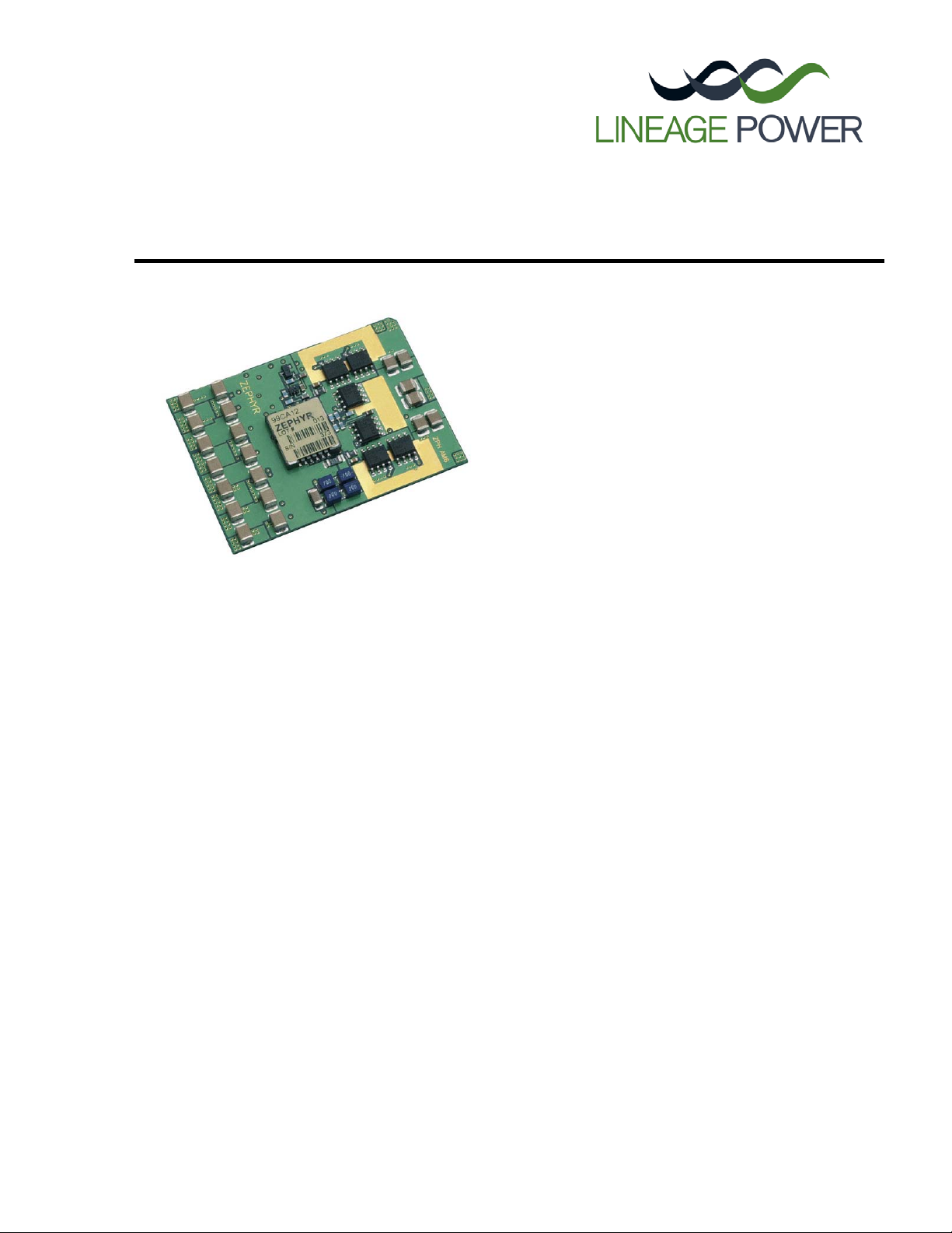
Titania™ Power Modules
Zephyr™ Non-Isolated SMT DC-DC Power Module:
0.8V to 3.5V @ 20A Output; 5V to 12V Input
RoHS Compliant
The Zephyr Power Module provides precise
voltage and very fast transient response in the
industry’s smallest footprint while offering very
high reliability and high efficiency.
Applications
Workstations
Servers
Desktop c omputers
Data processing applications
Distributed power architecture s
Telecommunications equipment
LAN/WAN applications
Description
The Zephyr Power Module is designed to meet the
precise voltage and fast transient requirements of
today’s and tomorrow’s high performance
microprocessor, DSP, memory boards and system level
applications in a distributed power architecture.
Advanced circuit techniques, high-frequency switching,
custom passive and active components, and very highdensity, surface-mount packaging technology deliver
high-quality, ultra compact, non-isolated DC-DC
conversion.
Features
Compliant to RoHS EU Directive 2002/95/EC (-Z
version)
Complian t to ROHS EU Directive 2002/95/EC with
lead solder exemption (non-Z versions)
Transient response met from 0A to rated full load
(up to 600 A/μS)
Exceeds VRM 8.x load transient requirements
No external bulk output capacitors required for
transient response
Wide input range 4.5 V to 12.6V
Wide output range 0.8V to 3.5V
Operation down to zero airflow
Small size and very low profile
Small size: ideal for minimizing motherboard area
in multiprocessor/multi-chip applications
High reliability: 200 FITs/5 million hour MTBF
Surface mount design shipped in JEDEC tray
Single control pin for margining
Single pin for output voltage setting
High efficiency
89% typical @ 16A, V
88% typical @ 18A, V
83% typical @ 20A, V
75% typical @ 20A, V
Remote sense
Programmable output voltage via resistor or
voltage source
Voltage trim capa bility using resistor
Output enable and module OK signals
Output overvoltage, overcurrent, short circuit, and
thermal protection
No heat sink require d
Low inductance surface-mount connections
UL* 1950 Recognized, CSA† C22.2 No. 950-95
Certified, and VDE 0805 (EN60950, IEC950)
Licensed. CE mark meets 73/23/EEC and
93/68/EEC directives
Dimensions: 52.32 mm x 37.08 mm x 5.66 mm
(2.06 in. x 1.460 in. x 0.223 in.)
Total weight: 15.5g (0.55 oz.)
IN = 5V, VOUT = 3.3V
IN = 5V, VOUT = 2.5V
IN = 5V, VOUT = 1.5V
IN = 5V, VOUT = 0.8V
‡
* UL is a registered trademark of Underwriters Laboratories,
Inc.
†
CSA is a registered trademark of Canadian Standards
Association.
‡
This product is intended for integration into end-use
equipment. All the required procedures for CE marking of
end-use equipment should be followed.
LINEAGE POWER 1
Page 2
Absolute Maximum Ratings
Stresses in excess of the absolute maximum ratings can cause permanent damage to the device. These are
absolute stress ratings only. Functional operation of the device is not implied at these or any other
conditions in excess of those given in the operations sections of the data sheet. Exposure to absolute
maximum ratings for extended periods can adversely affect device reliability.
Table 1. Absolute Maximum Ratings
Parameter Device Symbol Min Max Unit
Input Voltage (continuous)
OUTEN Terminal Voltage
Maximum Ambient
Storage Temperature
External Voltage applied
between V
ADJUST+ and VADJUST-
⎯
⎯
⎯
⎯
⎯
VIN – 0.5 13 V
VOUTEN – 0.5 6 V
TMAX
⎯
85 °C
VSTG – 40 150 °C
VEXT
0
3.5
V
Electrical Specifications
Table 2. Input Specifications
Parameter Device Symbol Min Typical Max Unit
Operating Input Voltage
Operating Input Current
• V
IN = 12V, VOUT = 3.3V,
I
OUT = 16A
• V
IN = 5V, VOUT = 3.3V,
I
OUT = 16A
∗
Depends on output voltage
⎯
⎯
⎯
VIN 4.5 12.6 V
I
IN
IIN
⎯
⎯
⎯
⎯
5.5
13.5
∗
∗
A
A
LINEAGE POWER 2
Page 3

Data Sheet
March 31, 2010
Table 3. Output Specifications (TA = 0 °C to 70 °C, VIN = 5V to 12V)
Output Voltage Set Point∗
Zephyr
% error = 1.4 + (0.75/V
V
∗
Static Regulation
Static output voltage variation measured at
output pins on system board with sense
pins connected to measured pins
1. Line Regulation
Output voltage variation as input voltage
changes from 5V to 12V with 50% load
2. Load Regulation
Output voltage variation as load changes
Zephyr Non-Isolated SMT DC-DC Power Module:
0.8V to 3.5V @ 20A Output, 5V to 12V Input
Parameter Symbol Min Typical Max Unit
+ 2.7/(13.44 + R
OUT = 3.3V
OUT [V])
ADJ[kΩ]) [%]
V
OUT
– 1.6
TRIM pin not connected
V
OUT
VOUT
⎯
⎯
from 0% to 100%
Transient Response, see Figures 5 – 16.
Measured as load changes from IOUT = 0A to
OUT = 16A at slew rate of ΔIOUT/Δt = 600 A/μs
I
1. Peak Deviation
• V
IN = 12V, 0.8V < VOUT < 1.3V
• V
IN = 12V, 1.5V < VOUT < 3.3V
• V
IN = 5V, 0.8V < VOUT < 1.3V
• V
IN = 5V, 1.5V < VOUT < 3.3V
2. Setting Time (time until V
OUT returns to
10% of peak deviation)
• V
IN = 12V, 0.8V < VOUT < 3.3V
• V
IN = 5V, 0.8V < VOUT < 3.3V
Measured as load changes from IOUT = 16A to
OUT = 0A at slew rate of ΔIOUT/Δt = 600 A/μs
I
1. Peak Deviation
• V
IN = 12V, 0.8V < VOUT < 1.3V
• V
IN =12V, 1.5V < VOUT < 3.3V
• V
IN = 5V, 0.8V < VOUT < 1.3V
• V
IN = 5V, 1.5V < VOUT < 3.3V
2. Setting Time (time until V
OUT returns to
10% of peak deviation)
• V
IN = 12V, 0.8V < VOUT < 3.3V
• V
IN = 5V, 0.8V < VOUT < 3.3V
VOUT
V
OUT
V
OUT
V
OUT
T
SET1
T
SET1
VOUT
V
OUT
V
OUT
V
OUT
T
SET2
TSET2
⎯
⎯
⎯
⎯
⎯
⎯
⎯
⎯
⎯
⎯
⎯
⎯
⎯
1
1
– 50
– 60
– 70
– 80
30
40
60
70
80
90
30
40
1.6
⎯
⎯
⎯
⎯
⎯
⎯
⎯
⎯
⎯
⎯
⎯
⎯
⎯
⎯
%
mV
mV
mV
mV
mV
mV
μs
μs
mV
mV
mV
mV
μs
μs
LINEAGE POWER 3
Page 4

Zephyr Non-Isolated SMT DC-DC Power Module:
0.8V to 3.5V @ 20A Output, 5V to 12V Input
Table 3. Output Specifications (TA = 0 °C to 70 °C, VIN = 5V to 12V), continued
Output Voltage Ripple and Noise, see
Figures 17 – 20. Measured with I
1. RMS Value
• V
IN = 12V, 0.8V < VOUT < 1.8V
• V
IN = 12V, 2.0V < VOUT < 3.3V
• V
IN = 5V, 0.8V < VOUT < 3.3V
2. Peak-to-peak (DC to 100 MHz)
• V
IN = 12V, 0.8V < VOUT < 2.0V
• V
IN = 12V, 2.5V < VOUT < 3.3V
• V
IN = 5V, 0.8V < VOUT < 3.3V
Total Regulation
Maximum output voltage error in static or
transient condition including ripple and
noise
OUT = 0.8V
• V
• V
OUT = 1.3V
• V
OUT = 1.5V
• V
OUT = 1.8V
• V
OUT = 2.0V
• V
OUT = 2.5V
• V
OUT = 3.3V
Maximum Output Current, depends on
output voltage. See thermal derating curves
for details, Figures 26 – 37.
Airflow: 0 LFM – 400 LFM
Ambient: 25 °C – 70 °C
• V
IN = 5V
• V
IN = 12V
Efficiency, see Figures 38 – 39
T
A = 25 °C, 0 LFM, IOUT = 16A
• V
OUT = 2.5V
V
V
• V
V
V
IN = 12V
IN = 5V
OUT = 0.8V
IN = 12V
IN = 5V
OUT = 16A.
VOUT/RMS
VOUT/RMS
VOUT/RMS
V
OUT/p-p
VOUT/p-p
VOUT/p-p
VOUT
VOUT
VOUT
VOUT
VOUT
VOUT
VOUT
IOUT
IOUT
η
η
η
η
⎯
⎯
⎯
⎯
⎯
⎯
– 104
– 113
– 126
– 131
– 133
– 144
– 152
14
13
⎯
⎯
⎯
⎯
4
5
3
16
20
10
⎯
⎯
⎯
⎯
⎯
⎯
⎯
⎯
⎯
86
89
73
78
Data Sheet
March 31, 2010
⎯
⎯
⎯
⎯
⎯
⎯
mVrms
mVrms
mVrms
114
123
136
141
143
154
162
26
24
⎯
⎯
⎯
⎯
mV
mV
mV
mV
mV
mV
mV
mV
mV
mV
A
A
%
%
%
%
LINEAGE POWER 4
Page 5

Data Sheet
March 31, 2010
Table 3. Output Specifications (TA = 0 °C to 70 °C, VIN = 5V to 12V), continued
Efficiency, see Figures 40 – 41
T
V
V
V
V
Zephyr Non-Isolated SMT DC-DC Power Module:
0.8V to 3.5V @ 20A Output, 5V to 12V Input
A = 60 °C, 300 LFM, IOUT = 16A
• V
OUT = 2.5V
IN = 12V
IN = 5V
• V
OUT = 0.8V
IN = 12V
IN = 5V
η
η
η
η
⎯
⎯
⎯
⎯
86
88
71
77
⎯
⎯
⎯
⎯
%
%
%
%
Output Current Slew Rate
Step function current from I
16A with no external load capacitors
OUT = 0A to
External Load Capacitance∗
(NOT REQUIRED FOR TRANSIENT RESPONSE)
• VIN = 12V
V
V
V
V
V
V
V
• V
V
V
V
V
V
V
V
∗
Maximum capacitance on output into which
OUT = 0.8V
OUT = 1.3V
OUT = 1.5V
OUT = 1.8V
OUT = 2.0V
OUT = 2.5V
OUT = 3.3V
IN = 5V
OUT = 0.8V
OUT = 1.3V
OUT = 1.5V
OUT = 1.8V
OUT = 2.0V
OUT = 2.5V
OUT = 3.3V
module can start with maximum current
Output Current-limit Inception, for IOUTMAX at
25 °C, 400 LFM. See thermal derating
curves, Figures 26 – 37
Turn-on Response Time, see Figures 1 – 2
Measured at I
OUT = 16A and with maximum
external load capacitor as specified above
ΔI
OUT/Δt
CL
CL
C
L
CL
CL
CL
CL
CL
CL
CL
CL
CL
CL
CL
IOUTLIM
ON — 5.0 10.0
T
0
0
0
0
0
0
0
0
0
0
0
0
0
0
0
105
—
—
—
—
—
—
—
—
—
—
—
—
—
—
—
⎯
600
10,000
6,800
3,300
1,000
1,000
1,000
1,000
10,000
10,000
6,800
3,300
3,300
3,300
1,000
160
A/µs
μF
μF
μF
μF
μF
μF
μF
μF
μF
μF
μF
μF
μF
μF
% IOUTMAX
ms
General Specifications
Table 4. Calculated FIT Rate and Weight
Parameter Min Typ Max Unit
Calculated FIT Rate — — 200 Per 109 device hours
Weight — — 15.5 (0.55) grams (oz.)
LINEAGE POWER 5
Page 6

Zephyr Non-Isolated SMT DC-DC Power Module:
v
v
v
V
,
V
,
0.8V to 3.5V @ 20A Output, 5V to 12V Input
Data Sheet
March 31, 2010
Safety Considerations
Module’s printed circuit board meets the standards of UL flammability specificatio ns per UL94V-0.
Feature Descriptions
Static Voltage Regulation
The output voltage measured at the converter output pins on the system board will be within the range
shown in Table 3, except during turn-on and turn-off periods. The static limits apply to ambient temperatures
between 0 °C and 70 °C. Static voltage regulation includes:
• DC output initial voltage and set point adjust
• Output load ranges specified in tables above
• Temperature and warm-up input voltage tolerances specified in input voltage and current
Turn-on Response Time
The output voltage will be within the specified range within 10 ms of the input voltage reaching 90% of its
nominal value with O
be inside its specified range within 10 ms. Figure 1 and Figure 2 represent typical start-up waveforms with
the maximum load current and load capacitor on the output indicated in Table 3. A pull-up resi stor of 10 kΩ
is used between Module OK pin and 5V.
UTEN present. When OUTEN is applied with input voltage present, the output voltage will
OUTEN, 5 V/div OUTEN, 5 V/di
MODULE OK, 5 V/di
OUT
0.5 V/div
2 ms/div 2 ms/div
MODULE OK, 5 V/di
OUT
1.0 V/div
Figure 1. Turn-on Waveform: V
OUT = 0.8V, 16A resistive load + 10,000 μF VOUT = 3.3V, 16A resistive load + 1,000 μF
V
IN = 12V, Figure 2. Turn-on Waveform: VIN = 5V,
LINEAGE POWER 6
Page 7
Data Sheet
March 31, 2010
Zephyr Non-Isolated SMT DC-DC Power Module:
0.8V to 3.5V @ 20A Output, 5V to 12V Input
Overshoot at Turn-on or Turn-off
Overshoot in application or removal of the input voltage, or application or removal of the O
UTEN signal is 5%
above the initially set output voltage. No negative voltage will be present on the output during turn-on or
turn-off.
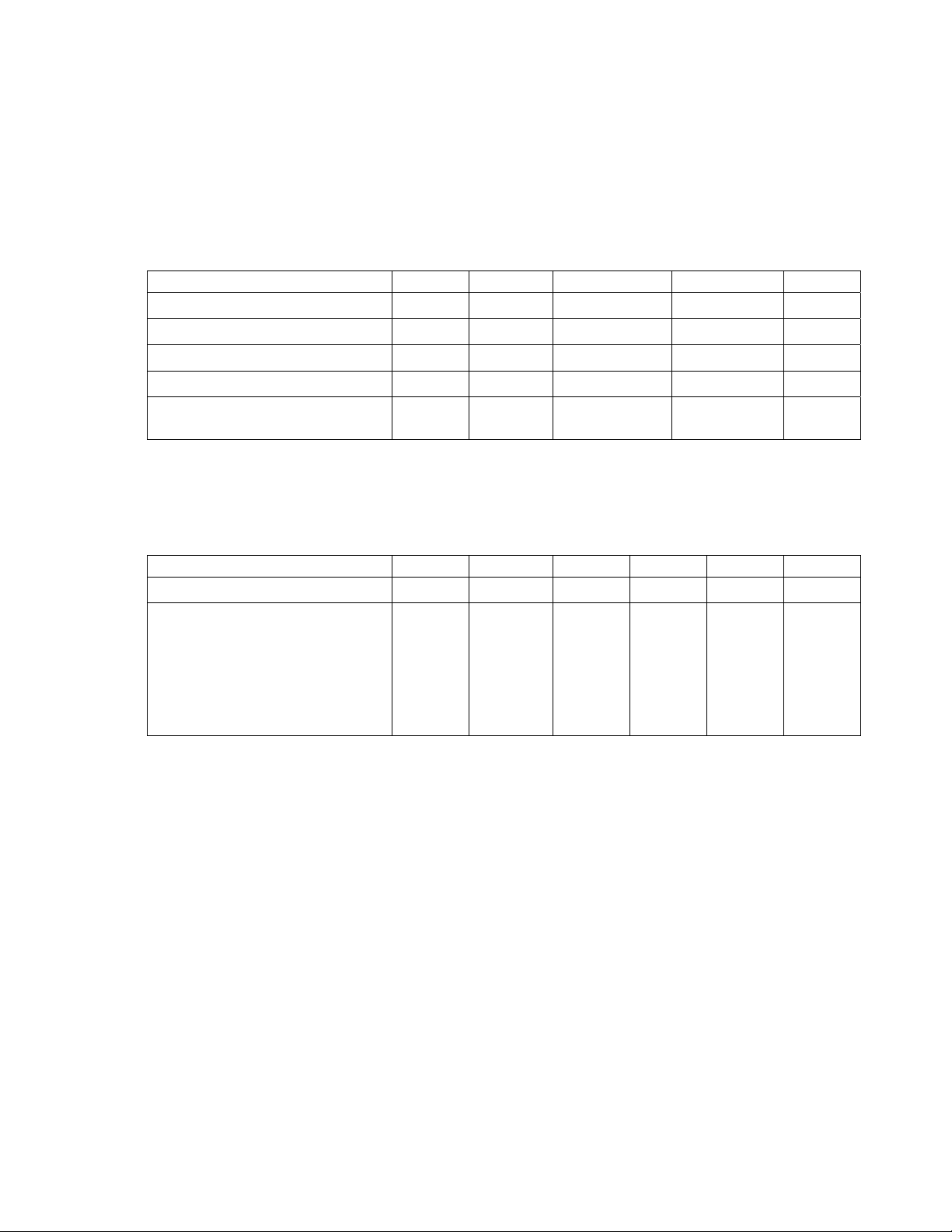
Module OK
An open collector signal with 2.0 mA current sinking capability is provided. The signal is in the low
impedance (less than 250Ω) state whenever V
is no input voltage, and in the open (more than 100 kΩ) state whenever V
The Module OK pin has an internal 0.1
μF capacitor connected to the output voltage return (GND).
OUT is off by more than ± 11% from its nominal value or there
OUT is within its specified range.
P-1 MOD_OK
Isink < 2mA
0.1u
Figure 3. Module OK Circuitry
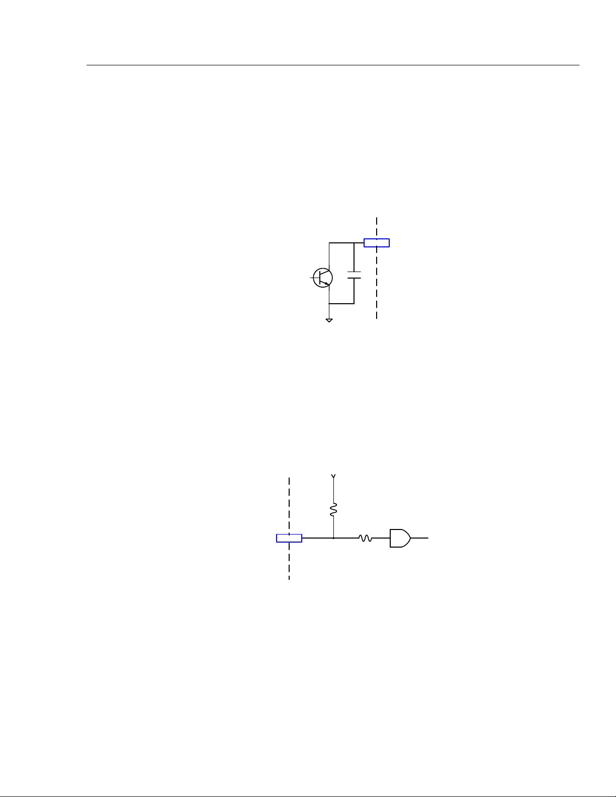
Output Enable — OUTEN
The module will accept an open collector signal consistent with TTL DC specifications for controlling the
output voltage. The module is enabled when this signal is above 2.0V and disabled when this signal is less
than 0.8V. The module does not source this signal with more than 0.6 mA. It is referenced to output voltage
return (G
ND).
+5V
10k
P-2OUTEN
820
Figure 4. Output Enable Circuitry
LINEAGE POWER 7
Page 8
Zephyr Non-Isolated SMT DC-DC Power Module:
0.8V to 3.5V @ 20A Output, 5V to 12V Input
Data Sheet
March 31, 2010
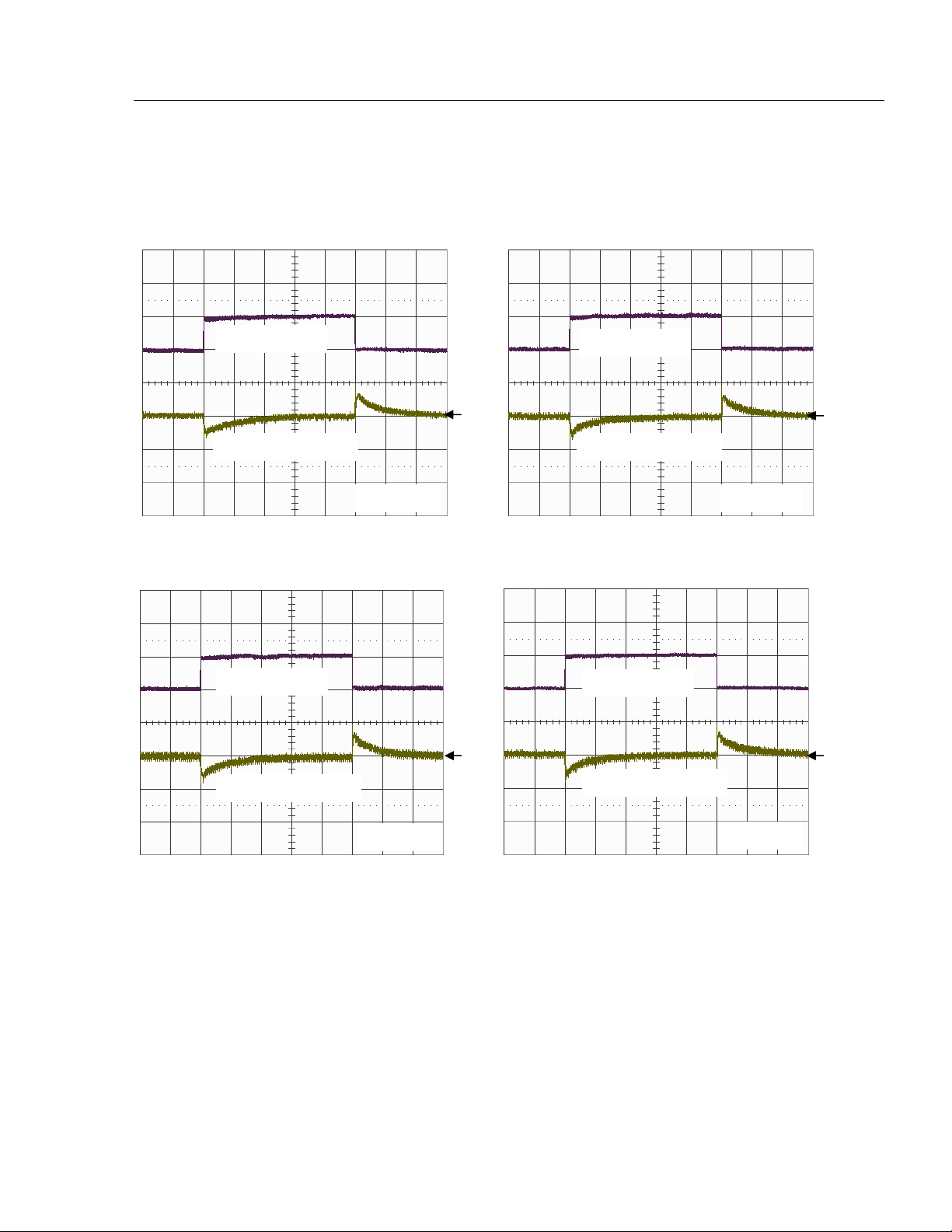
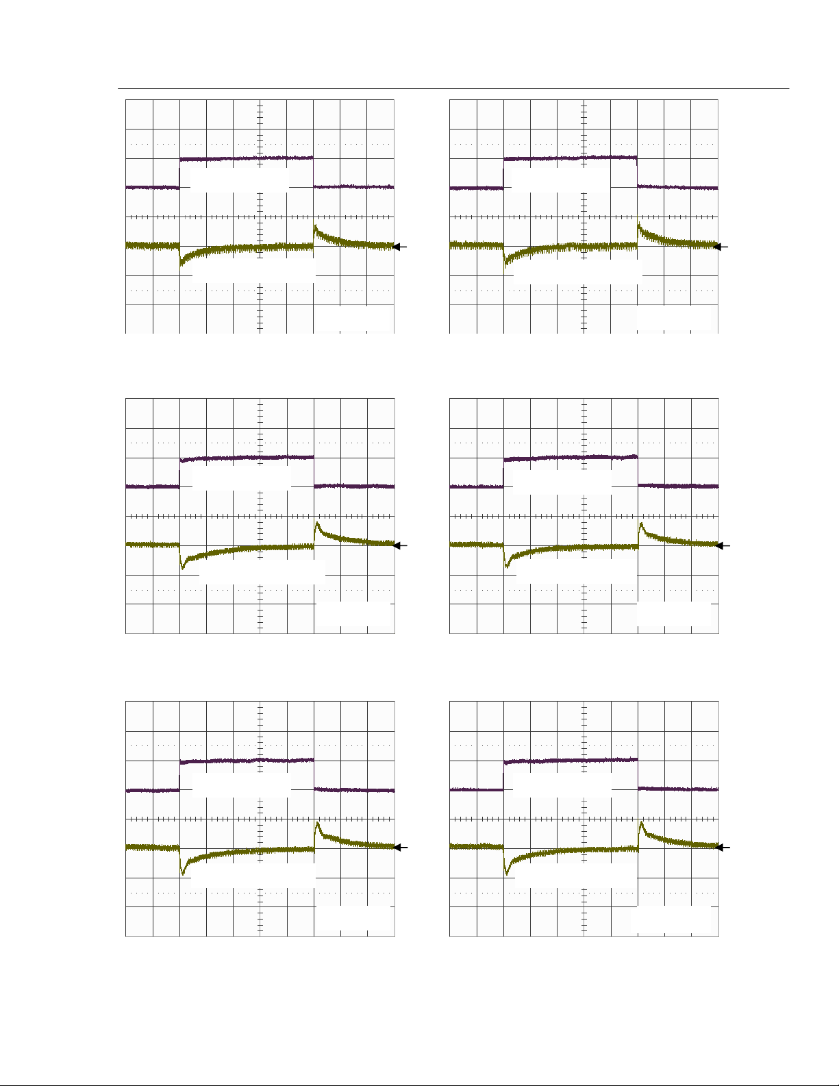
Transient Response
The output voltage measured at the converter output pins on the system board is within the transient range
shown in Table 3. The transient response is measured with DC – 200 MHz frequency band width, and at
ambient temperatures between 0 °C and 70 °C.
Typical transient response and noise waveforms are shown in Figures 5 – 16.
IOUT, 16 A/div
0.8 V
VOUT, 100 mV/div
20 μs/div 20 μs/div
IOUT, 16 A/div
VOUT, 100 mV/div
Figure 5. Transient Response: VIN = 12V, Figure 6. Transient Response: VIN = 12V,
OUT = 0.8V, ΔI = 16A, dI/dt = 600 A/μs VOUT = 1.3V, ΔI = 16A, dI/dt = 600 A/μs
V
IOUT, 16 A/div
1.8 V
VOUT, 100 mV/div
IOUT, 16 A/div
VOUT, 100 mV/div
1.3 V
2.0 V
20 μs/div
20 μs/div
Figure 7. Transient Response: VIN = 12V, Figure 8. Transient Response: VIN = 12V,
OUT = 1.8V, ΔI = 16A, dI/dt = 600 A/μs VOUT = 2.0V, ΔI = 16A, dI/dt = 600 A/μs
V
LINEAGE POWER 8
Page 9
Data Sheet
March 31, 2010
Zephyr Non-Isolated SMT DC-DC Power Module:
0.8V to 3.5V @ 20A Output, 5V to 12V Input
IOUT, 16 A/div IOUT, 16 A/div
2.5 V
VOUT, 100 mV/div
20 μs/div
VOUT, 100 mV/div
20 μs/div
Figure 9. Transient Response: V
OUT = 2.5V, ΔI =16A, dI/dt = 600 A/μs VOUT = 3.3V, ΔI = 16A, dI/dt = 600 A/μs
V
IN = 12V, Figure 10. Transient Response: VIN = 12V,
IOUT, 16 A/div
0.8 V
VOUT, 100 mV/div
20 μs/div 20 μs/div
IOUT, 16 A/div
VOUT, 100 mV/div
Figure 11. Transient Response: V
OUT = 0.8V, ΔI = 16A, dI/dt = 600 A/μs VOUT = 1.3V, ΔI = 16A, dI/dt = 600 A/μs
V
IN = 5V, Figure 12. Transient Response: VIN = 5V,
3.3 V
1.3 V
IOUT, 16 A/div IOUT, 16 A/div
1.8 V 2.0 V
VOUT, 100 mV/div VOUT, 100 mV/div
20 μs/div 20 μs/div
20 μs/div
Figure 13. Transient Response: V
OUT = 1.8V, ΔI = 16A, dI/dt = 600 A/μs VOUT = 2.0V, ΔI = 16A, dI/dt = 600 A/μs
V
LINEAGE POWER 9
IN = 5V, Figure 14. Transient Response: VIN = 5V,
Page 10

Zephyr Non-Isolated SMT DC-DC Power Module:
0.8V to 3.5V @ 20A Output, 5V to 12V Input
IOUT, 16 A/div IOUT, 16 A/div
2.5 V 3.3 V
VOUT, 100 mV/div VOUT, 100 mV/div
Data Sheet
March 31, 2010
20 μs/div 20 μs/div
Figure 15. Transient Response: V
OUT = 2.5V, ΔI = 16A, dI/dt = 600 A/μs VOUT = 3.3V, ΔI = 16A, dI/dt = 600 A/μs
V
IN = 5V, Figure 16. Transient Response: VIN =5V,
Output Voltage Ripple and Noise
Output voltage ripple and noise are defined as periodic or random signals measured at the output pins on
the system board with DC – 200 MHz frequency bandwidth and constant load. Figures 17 – 20 represent
output voltage ripple and noise at characteristic input and output voltages, measured with 200 MHz
bandwidth and 16A constant current load.
VOUT, 10 mV/div VOUT, 10 mV/div
0.5 μs/div 0.5 μs/div
Figure 17. Output Voltage Ripple and Noise: Figure 18. Output Voltage Ripple and Noise:
IN = 12V, VOUT = 0.8V, 16A static load VIN = 12V, VOUT = 3.3V, 16A static load
V
LINEAGE POWER 10
Page 11

Data Sheet
March 31, 2010
VOUT, 10 mV/div VOUT, 10 mV/div
Zephyr Non-Isolated SMT DC-DC Power Module:
0.8V to 3.5V @ 20A Output, 5V to 12V Input
0.5 μs/div 0.5 μs/div
Figure 19. Output Voltage Ripple and Noise: Figure 20. Output Voltage Ripple and Noise:
IN = 5V, VOUT = 0.8V, 16A static load VIN = 5V, VOUT = 3.3V, 16A static load
V
Input Voltage Ripple and Noise
Power
Source
1000 μF Electrolytic Cap.
Trace Inductance
1 μF Ceramic Cap.
Zephyr M odule
Load
Figure 21. Test Circuit for Input Voltage Ripple and Noise Measurement
Figures 22 – 25 represent input voltage ripple and noise, measured at the input pins of the system board at
characteristic input and output voltages with 200 MHz bandwidth, under 16A constant current load. The
measurement was made using 50Ω coax cable terminated with 50Ω at the oscilloscope. The input
capacitance consists of two Nichicon PL electrolytic capacitors, 1000 μF/16V each. The printed wiring board
(PWB) trace inductance is 2.1 nH. A ceramic capacitor of 1 μF is attached to the measurement point (input
pins on the system board, see Figure 21).
LINEAGE POWER 11
Page 12

Zephyr Non-Isolated SMT DC-DC Power Module:
0.8V to 3.5V @ 20A Output, 5V to 12V Input
VIN, 100 mV/div VIN, 100 mV/div
Data Sheet
March 31, 2010
0.5 μs/div
0.5 μs/div
Figure 22. Input Voltage Ripple and Noise: Figure 23. Input Voltage Ripple and Noise:
IN = 12V, VOUT = 0.8V, 16A static load VIN = 12V, VOUT = 3.3V, 16A static load
V
VIN, 100 mV/div VIN, 100 mV/div
0.5 μs/div 0.5 μs/div
Figure 24. Input Voltage Ripple and Noise: Figure 25. Input Voltage Ripple and Noise:
IN = 5V, VOUT = 0.8V, 16A static load VIN = 5V, VOUT = 3.3V, 16A static load
V
LINEAGE POWER 12
Page 13

Data Sheet
March 31, 2010
Zephyr Non-Isolated SMT DC-DC Power Module:
0.8V to 3.5V @ 20A Output, 5V to 12V Input
Thermal Ratings
Figures 26 – 37 show thermal derating curves for 12V and 5V input voltages, at different output voltages,
and with different ambient temperatures and airflow.
THERMAL DERATING 12 VIN / 0.8 VOUT
25
24
23
22
21
20
Output Current [A]
0 LFM
19
100 LFM
18
200 LFM
17
300 LFM
400 LFM
25 30 40 50 60 70
Ambient Temperature [°C]
Figure 26. Thermal Derating: VIN = 12V, VOUT = 0.8V Figure 27. Thermal Derating: VIN = 12V, VOUT = 1.3V Figure 26. Thermal Derating: VIN = 12V, VOUT = 0.8V Figure 27. Thermal Derating: VIN = 12V, VOUT = 1.3V
THERMAL DERATING 12 VIN / 1.8 VOUT
22
21
20
19
18
Output Current [A]
0 LFM
17
100 LFM
16
200 LFM
15
300 LFM
400 LFM
25 30 40 50 60 70
Ambient Temperature [°C]
Figure 28. Thermal Derating: VIN = 12V, VOUT = 1.8V Figure 29. Thermal Derating: VIN = 12V, VOUT = 2.0V Figure 28. Thermal Derating: VIN = 12V, VOUT = 1.8V Figure 29. Thermal Derating: VIN = 12V, VOUT = 2.0V
THERMAL DERATING 12 VIN / 2.5 VOUT
20
19
18
17
16
15
Output Current [A]
14
0 LFM
100 LFM
200 LFM
300 LFM
400 LFM
25 30 40 50 60 70
Ambient Temperature [°C]
Figure 30. Thermal Derating: VIN = 12V, VOUT = 2.5V Figure 31. Thermal Derating: VIN = 12V, VOUT = 3.3V Figure 30. Thermal Derating: VIN = 12V, VOUT = 2.5V Figure 31. Thermal Derating: VIN = 12V, VOUT = 3.3V
THERMAL DERATING 12 VIN / 1.3 VOUT
23
22
21
20
19
18
Output Current [A]
17
16
0 LFM
100 LFM
200 LFM
300 LFM
400 LFM
25 30 40 50 60 70
Ambient Temperature [°C]
THERMAL DERATING 12 VIN / 2.0 VOUT
22
21
20
19
18
0 LFM
17
Output Current [A]
100 LFM
16
200 LFM
15
300 LFM
400 LFM
25 30 40 50 60 70
Ambient Temperature [°C]
THERMAL DERATING 12 VIN / 3.3 VOUT
18.5
17.5
16.5
15.5
14.5
Output Current [A]
13.5
12.5
0 LFM
100 LFM
200 LFM
300 LFM
400 LFM
25 30 40 50 60 70
Ambient Temperature [°C]
LINEAGE POWER 13
Page 14

Zephyr Non-Isolated SMT DC-DC Power Module:
0.8V to 3.5V @ 20A Output, 5V to 12V Input
Data Sheet
March 31, 2010
THERMAL DERATING 5 VIN / 0.8 VOUT
THERMAL DERATING 5 VIN / 1.3 VOUT
27
26
25
24
23
Output Current [A]
0 LFM
22
100 LFM
21
200 LFM
20
300 LFM
400 LFM
25 30 40 50 60 70
Ambient Temperature [°C]
25
24
23
22
21
0 LFM
20
100 LFM
Output Current [A]
19
200 LFM
300 LFM
18
400 LFM
25 30 40 50 60 70
Ambient Temperature [°C]
Figure 32. Thermal Derating: VIN = 5V, VOUT = 0.8V Figure 33. Thermal Derating: VIN = 5V, VOUT = 1.3V
THERMAL DERATING 5 VIN / 1.8 VOUT
THERMAL DERATING 5 VIN / 2.0 VOUT
22
21
20
19
18
17
Output Current [A]
16
0 LFM
100 LFM
200 LFM
300 LFM
400 LFM
25 30 40 50 60 70
Ambient Temperature [°C]
22
21
20
19
0 LFM
18
100 LFM
17
Output Current [A]
200 LFM
16
300 LFM
400 LFM
25 30 40 50 60 70
Ambient Temperature [°C]
Figure 34. Thermal Derating: VIN = 5V, VOUT = 1.8V Figure 35. Thermal Derating: VIN = 5V, VOUT = 2.0V
THERMAL DERATING 5 VIN / 2.5 VOUT
THERMAL DERATING 5 VIN / 3.3 VOUT
20
19.5
19
18.5
18
17.5
17
16.5
16
Output Current [A]
15.5
15
0 LFM
100 LFM
200 LFM
300 LFM
400 LFM
25 30 40 50 60 70
Ambient Temperature [°C]
18.5
18
17.5
17
16.5
16
15.5
0 LFM
15
100 LFM
14.5
Output Current [A]
13.5
200 LFM
14
300 LFM
400 LFM
25 30 40 50 60 70
Ambient Temperature [°C]
Figure 36. Thermal Derating: VIN = 5V, VOUT = 2.5V Figure 37. Thermal Derating: VIN = 5V, VOUT = 3.3V
LINEAGE POWER 14
Page 15

Data Sheet
March 31, 2010
Zephyr Non-Isolated SMT DC-DC Power Module:
0.8V to 3.5V @ 20A Output, 5V to 12V Input
Efficiency
Figures 38 – 41 show typical efficiency charts for 12V and 5V input voltages, at different output voltages, and
with different ambient temperatures and airflow.
90
85
80
75
70
65
60
Total Efficiency [%]
55
50
2 4 6 8 10 12 14 16 18 20
0.8 Vout
1.3 Vout
1.5 Vout
1.8 Vout
2 Vout
2.5 Vout
3.3 Vout
Output Current [A]
90
85
80
75
70
65
60
Total Efficiency [%]
55
50
2 4 6 8 10 12 14 16 18
0.8 Vout
1.3 Vout
1.5 Vout
1.8 Vout
2 Vout
2.5 Vout
3.3 Vout
Output Current [A]
Figure 38. Efficiency: VIN = 12V, 25 °C, no airflow Figure 39. Efficiency: VIN = 12V, 60 °C, 300 LFM
95
90
85
80
75
70
Total Efficiency [%]
65
60
2468101214161820
0.8 Vout
1.3 Vout
1.5 Vout
1.8 Vout
2 Vout
2.5 Vout
3.3 Vout
Output Current [A]
95
90
85
80
75
70
Total Efficiency [%]
65
60
2 4 6 8 101214161820
0.8 Vout
1.3 Vout
1.5 Vout
1.8 Vout
2 Vout
2.5 Vout
3.3 Vout
Output Current [A]
Figure 40. Efficiency: V
IN = 5V, 25 °C, no airflow Figure 41. Efficiency: VIN = 5V, 60 °C, 300 LFM
LINEAGE POWER 15
Page 16

Zephyr Non-Isolated SMT DC-DC Power Module:
−
⋅
(
+
⋅
⋅
+
0.8V to 3.5V @ 20A Output, 5V to 12V Input
Data Sheet
March 31, 2010
Output control
There are two ways to set the output voltage of the Zephyr:
1. A resistor calculated from the following equation can be inserted between V
pin.
OUT
V
V
−
3.3
or
R
=
ADJ
44.33.3
=
For example, to get the output voltage of 2.5V, R
should be attached between these two pins.
Shorting and opening of these pins will give the output voltage of 0.844V and 3.30V, respectively. For the
output voltage beyond this range (up to ± %5), the use of T
The additional output voltage error due to the tolerance R
%
This error should be added to the error given in the “Output Voltage Set Point” section of Table 3 to get
the total DC output voltage error.
2. An external voltage V
voltage. The relation between V
V [%] (3)
V
OUT
⎛
⎜
⎜
=±
_
RADJOUT
EXT [V] can be applied between VADJUST + pin and VADJUST − pin to control output
V
OUT
44.13
⎜
44.3
⎜
⎜
⎝
+
OUT and VEXT is described as follows.
=
R
44.13
+
+
R
ADJ
R
ADJ
1035.11
35.1144.13
OUT
⋅
V
R
ADJ
EXT
[kΩ] (1)
)
ADJ
[V] (2)
ADJ = 27.8 kΩ, the closest standard resistor of 27.7 kΩ
RIM pin is recommended.
ADJ_TOL [%] of RADJ [kΩ] is described as follows.
R
⎛
⎜
144.3
R
ADJ
R
ADJ
[V] (4)
±⋅+
⎜
⎝
⎛
⎜
⎜
⎝
100
R
144.13
±⋅+
100
ADJUST + pin and VADJUST −
⎞
⎞
_
TOLADJ
_
TOLADJ
⎟
⎟
⎟
⎟
⎠
⎞
⎟
⎟
⎠
1001
⋅
−
⎟
⎟
⎟
⎠
44.13
Therefore, in order to set the output voltage to 2.5V, V
specified external voltage (such as DAC) is applied between V
voltage identification code with each corresponding voltage V
resulting output voltages of the module V
ADJUST- pins are open circuit, VOUT = 3.3V (default value).
and V
OUT calculated from the equation (4). Note that if the VADJUST+
EXT = 2.23V. The equation (4) is valid even when
ADJUST+ and VADJUST −. Table 5 shows
EXT supplied from standard DAC, as well as
LINEAGE POWER 16
Page 17

Data Sheet
March 31, 2010
Table 5. Voltage Identification Code with Output Voltage of Module
The additional output voltage error due to the tolerance V
This error should be added to the error given in the “Output Voltage Set Point” section of Table 3, using
ADJ = 0 kΩ, to get the total DC output voltage error.
R
Zephyr Non-Isolated SMT DC-DC Power Module:
0.8V to 3.5V @ 20A Output, 5V to 12V Input
VID Pins
EXT [ V ]
VID4 VID3 VID2 VID1 VID0
0 1 1 1 1 1.30 1.811
0 1 1 1 0 1.35 1.849
0 1 1 0 1 1.40 1.886
0 1 1 0 0 1.45 1.923
0 1 0 1 1 1.50 1.961
0 1 0 1 0 1.55 1.998
0 1 0 0 1 1.60 2.035
0 1 0 0 0 1.65 2.072
0 0 1 1 1 1.70 2.110
0 0 1 1 0 1.75 2.147
0 0 1 0 1 1.80 2.184
0 0 1 0 0 1.85 2.221
0 0 0 1 1 1.90 2.258
0 0 0 1 0 1.95 2.295
0 0 0 0 1 2.00 2.333
0 0 0 0 0 2.05 2.370
1 1 1 1 1 No Output 3.300
1 1 1 1 0 2.1 2.407
1 1 1 0 1 2.2 2.481
1 1 1 0 0 2.3 2.556
1 1 0 1 1 2.4 2.630
1 1 0 1 0 2.5 2.705
1 1 0 0 1 2.6 2.779
1 1 0 0 0 2.7 2.853
1 0 1 1 1 2.8 2.928
1 0 1 1 0 2.9 3.002
1 0 1 0 1 3.0 3.077
1 0 1 0 0 3.1 3.151
1 0 0 1 1 3.2 3.225
1 0 0 1 0 3.3 3.300
1 0 0 0 1 3.4 3.374
1 0 0 0 0 3.5 3.449
⎛
⎛
⎜
⎜
⎜
⎜
⎝
%
V
=±
_
VEXTOUT
⎜
⎜
V
V
⎛
⎜
V
EXT
()
±⋅⋅+
11035.11
⎜
⎝
⋅+
1035.11
V
EXT
⎜
⎝
VOUT [ V ]
EXT_TOL [%] of VEXT is described as follows:
⎞
_
TOLEXT
⎟
100
⎟
⎠
0 = Closed
(Connected to Ground)
1 = Open
⎞
⎞
⎟
⎟
⎟
⎟
⎠
−
⎟
[%] (5)
1001
⋅
⎟
⎟
⎠
LINEAGE POWER 17
Page 18

Zephyr Non-Isolated SMT DC-DC Power Module:
⋅−⋅
⋅−⋅
0.8V to 3.5V @ 20A Output, 5V to 12V Input
Data Sheet
March 31, 2010
Trim
RIM pin is provided to margin high/low the output voltage by certain percentages independent of the output
T
voltage. The equation to margin low by connecting a resistor, R
NOMOUT
VV
R
LOW
=
621654
OUTNOM
VV
⋅−⋅
22
To margin low by 2.5%, R
LOW = 332.0 kΩ. Shorting TRIM pin to OUTSENSE + pin provides the maximum
negative adjustment of 5.0%.
The equation to margin high by connecting a resistor, R
HIGH, from TRIM pin to OUTSENSE – pin is:
R
HIGH
=
588621
NOMOUT
VV
⋅−⋅
22
OUTNOM
VV
To margin high by 2.5%, R
HIGH = 365.0 kΩ. Shorting TRIM pin to OUTSENSE – pin provides the maximum
positive adjustment of 5.0%.
RIM is not connected to OUTSENSE + or OUTSENSE −, VOUT = VNOM.
If T
LOW, from TRIM pin to OUTSENSE + pin is:
[kΩ] (6)
[kΩ] (7)
LINEAGE POWER 18
Page 19

Data Sheet
March 31, 2010
Zephyr Non-Isolated SMT DC-DC Power Module:
0.8V to 3.5V @ 20A Output, 5V to 12V Input
Output Overvoltage Protection
Protection level: The converter provides overvoltage protection by latching off when the output
voltage rises beyond V
voltage. Care must be taken because the voltage increase due to T
contribute to V
Overvoltage protection circuit protects against shorted feedback/sense connections.
Voltage sequencing: No allowed variation of input voltages or output current or control signals will falsely
trigger an OVP event or damage the module.
TRIP.
TRIP. VTRIP is between 112% and 120% of the nominal output
RIM can also
Reset After Shutdown
If the module goes into an overvoltage shutdown state, the module cannot return to normal operation mode
even after the fault has been removed. Input voltage of the module must be reset to restart the module.
Output Overcurrent Protection
Overcurrent protection is provided to protect the module from damage caused by excessive output current.
Current overload is from 5% to 60% over the maximum output current values given in the thermal derating
curves (at 25 °C, 400 LFM, see thermal derating curves Figure 26 – 37). The module will shut down until the
overload is removed, and then will automatically restart.
Overtemperature Protection
The module is protected against failure from overtemperature conditions created by high ambient
temperature or by low or no airflow condition. It will either operate properly within the requirements or shut
down (nonlatching). The module will function as specified under overtemperature conditions until disabled
(nonlatching) by the protection circuit.
LINEAGE POWER 19
Page 20

Zephyr Non-Isolated SMT DC-DC Power Module:
0.8V to 3.5V @ 20A Output, 5V to 12V Input
Data Sheet
March 31, 2010
Remote Sense
The remote sense inputs (OUTSENSE + and OUTSENSE -) should be connected to the load, using separate
sense traces on the system board as shown in Figure 42. Remote sense can compensate for the total output
voltage drop by up to the amount indicated in Table 6. These values are calculated to prevent unwanted
overvoltage protection by the module under the worst possible voltage error listed in Table 3 (including
transient error). In the event of an open remote sense lines, the module will maintain local sense regulation
through 100Ω internal resistors connected to the V
OUT pins, with an additional + 0.3% DC error in VOUT.
Table 6. Maximum Remote Sense Compensation
V
OUT [V] VMAXCOMP [V]
0.8 0.02
1.3 0.10
1.5 0.12
1.8 0.16
2.0 0.19
2.5 0.26
3.3 0.38
VIN +
OUTSENSE +
OUT+
V
RTRACE +
Zephyr Module
Load
TRACE -
IN -
V
UTSENSE -
O
V
OUT-
R
Figure 42. Remote Sense Connection to Load
LINEAGE POWER 20
Page 21

Data Sheet
March 31, 2010
Zephyr Non-Isolated SMT DC-DC Power Module:
0.8V to 3.5V @ 20A Output, 5V to 12V Input
Environmental
Design including materials is consistent with environmental stan dards in Table 7.
Table 7. Environmental and Reliability Specifications
Temperature
Humidity
Ambient 0 °C to 70 °C at zero to
400 LFM, full load (see Thermal Ratings)
with a maximum rate of change of
5 °C/10 minutes minimum but no more
than 10 °C/hour
To 85% relative humidity To 95% relative humidity
Operating Nonoperating
Ambient – 40 °C to 70 °C with a maximum rate
of change of 20 °C/hour (Thermal shock of
– 40 °C to 70 °C, 10 cycles; transfer time shall
not exceed 5 minutes; duration of exposure to
temperature extremes shall be 20 minutes)
(noncondensing)
Altitude 0 to 10,000 feet 0 to 50,000 feet
Reliability
Calculated MTBF of 5 million hours assuming continuous operation at 55 °C, at 200 LFM
airflow nominal input voltage and 80% maximum load
EMI Complies with the limits of FCC Class B and VDE 243 Level B for radiated emissions
Electrostatic
discharge
15 KV initialization level per specification
number EN61000-3-2. The direct ESD
event shall cause no out-of-regulation
conditions.
(Includes overshoot,
25 KV initialization level
undershoot, and nuisance trips of the
overvoltage protection, overcurrent
protection, or remote shutdown circuitry)
LINEAGE POWER 21
Page 22

Zephyr Non-Isolated SMT DC-DC Power Module:
0.8V to 3.5V @ 20A Output, 5V to 12V Input
Module Pin-out
The pin-out of Zephyr modules is indicated in
Figure 43 and Table 8.
Figure 43. Top View of Board
(Pins are located on the bottom side)
Table 8. Pin-out of Zephyr Module
1 MODULE OK
2 OUTEN
3 OUTSENSE 4 OUTSENSE+
5 VOUT +
6 VOUT -
7 VOUT +
8 VOUT -
9 VOUT +
10 VOUT 11 VOUT +
12 VOUT 13 VADJUST +
14 VADJUST 15 TRIM
16 RESERVED
17 VIN +
18 VIN +
19 VIN +
20 VIN 21 VIN 22 VIN -
Data Sheet
March 31, 2010
LINEAGE POWER 22
Page 23

Data Sheet
March 31, 2010
Zephyr Non-Isolated SMT DC-DC Power Module:
0.8V to 3.5V @ 20A Output, 5V to 12V Input
Mechanical Specifications
Mechanical specifications (Table 9) and module outline (Figure 44) are illustrated below. The pin layout and
the recommended pad size are shown in Figure 45 and Figure 46.
Table 9. Mechanical Specifications
Parameter Symbol Min Typical Max Unit
Physical Size L
W
H
—
—
—
37.08 (1.460)
52.32 (2.060)
5.66 (0.223)
37.21 (1.465)
52.45 (2.065)
6.12 (0.241)
Weight — — — 15.5 (0.55) grams (oz.)
0.223 [5.66] NOM.
0.241 [6.12] MAX.
mm (in.)
mm (in.)
mm (in.)
DATE CODE
ZEPHYR
LOT NUM.
SERIAL NUM.
L
T
u
e
c
c
e
h
n
n
t
o
lo
g
ie
s
Z
E
P
H
Y
R
Z
P
H
A
M
2
P22
P21
P20
P19
P18
P17
P1
P16 P15
P2
P5
P3
P4
P6
P7
P8
P9
P10
P11
P13P1 4
P12
Figure 44. Outline of Zephyr Module
LINEAGE POWER 23
Page 24

Zephyr Non-Isolated SMT DC-DC Power Module:
0.8V to 3.5V @ 20A Output, 5V to 12V Input
P1 P2
P22
P21
P20
P19
P18
P17
P16 P15
Data Sheet
March 31, 2010
P5
P4P3
P6
P7
P8
P9
P10
P11
P13P1 4
P12
Figure 45. Pin Layout of Zephyr Module
Recom mended PAD Size and Layout
P5
P6
P7
P8
P9
P10
P11
P12
P4 P3
P13 P14
P1P2
P22
P21
P20
P19
P18
P17
P16P1 5
Figure 46. Recommended Pad Size and Layout
LINEAGE POWER 24
Page 25

Data Sheet
March 31, 2010
Zephyr Non-Isolated SMT DC-DC Power Module:
0.8V to 3.5V @ 20A Output, 5V to 12V Input
Fusing Considerations
A 10A fuse is required for input voltages of 10.6V and higher. It is not required for input voltages below
10.6V. The following fuse or equivalent is recommended:
2
Characteristic Fuse Parameter Littlefuse R451010 Nano
SMF
Fuse Current Rating 10A 10A
Voltage Rating 32 minimum 125
I2t 100 a2sec maximum 26.4 a2sec
DC Interruption Rating
(must be DC rated, not just
35A minimum 35A
AC rated)
UL Recognized Mandatory Yes
The fuse should be located in the input voltage bus side of the input capacitor to minimize inductance
between the input capacitor and the Zephyr Power Module. The fuse shoul d not be located in proximity to
any object which might abnormally ‘preheat’ the fuse, causing undesired melting.
The Zephyr Power Module begins regulating with an input voltage above approximately 4V and will draw
more input current at lower voltages. If the input voltage rise times and fall times are too slow, shorter fuse
life and nuisance opening may occur. To minimize such fuse input current stresses, the module should be
enabled after input voltage is applied and disabled before input voltage is removed, by using the OUTEN pi n.
Fuse, 10A
Minimize this
distance and
inductance
V
IN+
Zephyr Module
DC
Input
Bus
To other
modules
or circuits
Input
Capacitor
V
IN -
OUTEN
Figure 47. Fuse Placement
LINEAGE POWER 25
Page 26

Zephyr Non-Isolated SMT DC-DC Power Module:
0.8V to 3.5V @ 20A Output, 5V to 12V Input
Data Sheet
March 31, 2010
Surface Mount Information
Pick and Place
The Zephyr SMT modules use an open frame construction and are designed for a fully automated assembly
process. The modules are fitted with a label designed to provide a large surface area for pick and place
operations. The label meets all the requirements for surface mount processing, as well as safety standards,
and is able to withstand reflow temperatures of up to 300
as product code, serial number and the location of manufacture.
Nozzle Recommendations
The module weight has been kept to a minimum by using open frame construction. Even so, these modules
have a relatively large mass when compared to conventional SMT components. Variables such as nozzle
size, tip style, vacuum pressure and placement speed should be considered to optimize this process. The
minimum recommended nozzle diameter for reliable operation is 6mm. The maximum nozzle outer diameter,
which will safely fit within the allowable component spacing, is 9 mm. Oblong or oval nozzles up to 11 x 9
mm may also be used within the space available.
Tin Lead Soldering
The Zephyr SMT power modules are lead free modules and can be soldered either in a lead-free solder
process or in a conventional Tin/Lead (Sn/Pb) process. It is recommended that the customer review data
sheets in order to customize the solder reflow profile for each application board assembly. The following
instructions must be observed when soldering these units. Failure to observe these instructions may result
in the failure of or cause damage to the modules, and can adversely affect long-term reliability.
In a conventional Tin/Lead (Sn/Pb) solder process peak reflow temperatures are limited to less than 235
Typically, the eutectic solder melts at 183
o
C, wets the land, and subsequently wicks the device connection.
Sufficient time must be allowed to fuse the plating on the connection to ensure a reliable solder joint. There
are several types of SMT reflow technologies currently used in the industry. These surface mount power
modules can be reliably soldered using natural forced convection, IR (radiant infrared), or a combination of
convection/IR. For reliable soldering the solder reflow profile should be established by accurately measuring
the modules CP connector temperatures.
Lead Free Soldering
The –Z version Austin SuperLynx II SMT modules are lead-free (Pb-free) and RoHS compliant and are both
forward and backward compatible in a Pb-free and a SnPb soldering process. Failure to observe the
instructions below may result in the failure of or cause damage to the modules and can adversely affect longterm reliability.
o
C. The label also carries product information such
o
C.
LINEAGE POWER 26
Page 27

Data Sheet
March 31, 2010
Zephyr Non-Isolated SMT DC-DC Power Module:
0.8V to 3.5V @ 20A Output, 5V to 12V Input
300
250
200
150
10 0
REFLOW TEMP (°C)
50
0
Peak Temp 235oC
Hea t zone
oCs-1
max 4
Soak zone
30-240s
Preheat zone
oCs-1
max 4
REFLOW TIME (S)
T
lim
205
Cooling
zone
1- 4
above
o
C
oCs-1
Figure 48. Reflow Profile for Tin/Lead (Sn/Pb) process
240
235
230
225
220
215
210
MAX TEMP SOLDER (°C)
205
200
0 102030405060
Figure 49. Time Limit Curve Above 205
o
C for Tin/Lead (Sn/Pb) process
Pb-free Reflow Profile
Power Systems will comply with J-STD-020 Rev. C (Moisture/Reflow Sensitivity Classification for
Nonhermetic Solid State Surface Mount Devices) for both Pb-free solder profiles and MSL classification
procedures. This standard provides a recommended forced-air-convection reflow profile based on the
volume and thickness of the package. The suggested Pb-free solder paste is Sn/Ag/Cu (SAC). The
recommended linear reflow profile using Sn/Ag/Cu solder is shown in Fig. 50.
300
Per J-STD-020 Rev. C
250
200
150
100
Reflow Temp (°C)
50
0
Heating Zone
1°C/Se c o nd
Peak Temp 260°C
* Min. Time Above 235°C
15 Seco nds
*Time Above 217°C
60 Seco nds
Reflow Time (Seconds)
Cooling
Zone
Figure 50. Recommended linear reflow profile using Sn/Ag/Cu solder.
LINEAGE POWER 27
Page 28

Zephyr Non-Isolated SMT DC-DC Power Module:
0.8V to 3.5V @ 20A Output, 5V to 12V Input
Data Sheet
March 31, 2010
MSL Rating
The Zephyr SMT modules have a MSL rating of 1.
Storage and Handling
The recommended storage environment and handling procedures for moisture-sensitive surface mount
packages is detailed in J-STD-033 Rev. A (Handling, Packing, Shipping and Use of Moisture/Reflo w
Sensitive Surface Mount Devices). Moisture barrier bags (MBB) with desiccant are required for MSL ratings
of 2 or greater. These sealed packages should not be broken until time of use. Once the original package is
broken, the floor life of the product at conditions of ≤ 30°C and 60% relative humidity varies according to the
MSL rating (see J-STD-033A). The shelf life for dry packed SMT packages will be a minimum of 12 months
from the bag seal date, when stored at the following conditions: < 40° C, < 90% relative humidity.
Post Solder Cleaning and Drying Considerations
Post solder cleaning is usually the final circuit-board assembly process prior to electrical board testing. The
result of inadequate cleaning and drying can affect both the reliability of a power module and the testability of
the finished circuit-board assembly. For guidance on appropri ate soldering, cleaning and drying procedures,
refer to Board Mounted Power Modules: Soldering and Cleaning Application Not e (AN0 4-001).
LINEAGE POWER 28
Page 29

Data Sheet
a
©
March 31, 2010
Zephyr Non-Isolated SMT DC-DC Power Module:
0.8V to 3.5V @ 20A Output, 5V to 12V Input
Ordering Information
Please contact your Lineage Power Account Manager or Field Application engineer for pricing and
availability.
Table 10. Coding Scheme for Ordering
Product Description Comcode Expanded Product Description
5 V
IN to12 VIN; 0.8 VOUT to 3.3 VOUT; 20 A IOUT;
Zephyr 5/12 V 0.8/3.5 V 20A J 108601220
ZRA020A0F-VZ 108995148
-Z version refers to RoHS-compliant code.
Zephyr Power Modules are shipped in packages of four JEDEC tra y s with fifteen modules per tray.
World Wide Headquarters
Lineage Power Corporation
601 Shiloh Road, Plano, TX 75074, USA
+1-800-526-7819
(Outside U.S.A.: +1-972-244-9428)
www.lineagepower.com
e-mail: techsupport1@lineagepower.com
Lineage Power reserves the right to make changes to the product(s) or information contained herein without notice. No liability is assumed as a result of their use or
pplication. No rights under any patent accompany the sale of any such product(s) or information.
Lineage Power DC-DC products are protected under various patents. Information on these patents is available at www.lineagepower.com/patents.
2009 Lineage Power Corporation, (Plano, Texas) All International Rights Reserved.
LINEAGE POWER 29
600 A/μsec transient rate; surface mount LISMC
connector; JEDEC tray package
IN to12 VIN; 0.8 VOUT to 3.3 VOUT; 20 A IOUT;
5 V
600 A/μsec transient rate; surface mount LISMC
connector; JEDEC tray package
RoHS Compliant
Asia-Pacific Headquarters
Tel: +65 6593 7211
Europe, Middle-East and Africa Headquarters
Tel: +49 898 780 672 80
India Headquarters
Tel: +91 80 28411633
Document No: DS03-076 ver 1.4
PDF name: zephyr.pdf
 Loading...