

GE Industrial Solutions WattStation Pedestal EVSE Charger MODBUS Register Mapping Guide User Manual
Page 1

GE Energy
TM
GE WattStation
EVSE Charger
MODBUS Register Mapping Guide
Pedestal
Page 2

WattStationTM EV Charger MODBUS Register Guide
CCOONNTTEENNTTSS
1! Publications........................................................................................................................................................................................... 3!
2! MODBUS Communication Overview .........................................................................................................................................4!
2.1! General Overview...............................................................................................................................................................................4!
2.2! MODBUS/TCP Overview................................................................................................................................................................... 6!
3! EVSE MODBUS Communication Architecture....................................................................................................................... 7!
3.1! MODBUS/TCP Communication Topologies ............................................................................................................................ 7!
3.2! MODBUS Access Control................................................................................................................................................................. 9!
3.3! MODBUS Function Codes Supported........................................................................................................................................ 9!
3.4! MODBUS Exception Codes Supported....................................................................................................................................13!
3.5! MODBUS Operations.......................................................................................................................................................................14!
4! EVSE MODBUS Register Map.......................................................................................................................................................14!
4.1! EVSE MODBUS Register Data Module Information Registers......................................................................................14!
4.2! EVSE MODBUS Operation Status Registers..........................................................................................................................16!
4.3! EVSE Identification Register ........................................................................................................................................................17!
4.4! EVSE Current Charging Information Diagnostic Registers ...........................................................................................18!
4.5! EVSE MODBUS Diagnostic Registers .......................................................................................................................................20!
4.6! EVSE MODBUS Connection Table Diagnostic Registers.................................................................................................21!
4.7! Summary of EVSE MODBUS Data Registers ........................................................................................................................23!
!
2 GE Energy ©2012 GE Company All Rights Reserved
Page 3

Reeff.. NNoo..
WattStationTM EV Charger MODBUS Register Guide
1 Publications
Reference Documents
R
DEH - 41579 WattStationTM Pedestal Installation Manual
DEH - 41580 WasttStationTM Pedestal User Manual
TTiittllee
3 GE Energy ©2012 GE Company All Rights Reserved
Page 4

WattStationTM EV Charger MODBUS Register Guide
Request
2 MODBUS Communication Overview
2.1 General Overview
MODBUS is an application layer messaging protocol for device communications over different types
of buses or networks. MODBUS communication adopts client and server model. MODBUS Client
initials the MODBUS communication by issuing MODBUS Request and the MODBUS Server processes
the request and sends back the MODBUS Response as shown in Figure 2.1.
MODBUS Client
MODBUS client/server model.
2.1.1 MODBUS Protocol Data Unit (PDU)
MODBUS protocol itself defines a simple protocol data unit ((PPDDUU)) independent of the underlying
communication layers as shown in Figure 2.2.
Function Code
MODBUS PDU format.
Figure - 2.2
Field Description
Function Code Tell MODBUS server what kind of action to perform. For some function
code, sub function code is added to define multiple actions.
Data Contains data information
4 GE Energy ©2012 GE Company All Rights Reserved
MODBUS
MODBUS
Response
Figure 2.1
MODBUS PDU
MODBUS PDU field description
Data
Table – 2.1
MODBUS Server
Page 5

WattStationTM EV Charger MODBUS Register Guide
2.1.2 MODBUS Application Data Unit (ADU)
Based on the underlying communication bus, additional bus related fields are added to the beginning
(and tailor) of the MODBUS PDU to form MODBUS Application Data Unit. Figure 2-3 shows a MODBUS
Serial ADU format. The MODBUS/TCP ADU format will be addressed in section 2.2.
MODBUS ADU
Address
Function Code
MODBUS RTU ADU format
Figure – 2.3
2.1.3 MODBUS Data Model
MODBUS uses a ‘big-Endian’ representation for addresses and data items. MODBUS data model maps
data into four different kinds of register ranges each of which has distinguishing characteristics as
shown in Table 2.2. Each MODBUS register is a 16 bits field.
Register Type Object Type Type of Access Comments
Coil Single bit Read-Write This data in this type of registers
Discrete Input Single bit Read-Only This type of data can be provided
Input Register 16 bits word Read-Only This type of data can be provided
Holding Register 16 bits word Read-Write This data in this type of registers
MODBUS data register types
Table – 2.2
Data
CRC
can be alterable by an application
program.
by an I/O system.
by an I/O system.
can be alterable by an application
program.
5 GE Energy ©2012 GE Company All Rights Reserved
Page 6

WattStationTM EV Charger MODBUS Register Guide
MUUSSTT
2.2 MODBUS/TCP Overview
MODBUS communication over TCP has already become a de-facto automation standard. Figure 2.4
shows the MODBUS/TCP ADU format.
MODBUS/TCP ADU format.
Figure – 2.4
A dedicated header called the MBAP header (MODBUS Application Protocol header) is used to identify
the MODBUS/TCP Application Data Unit as Figure 2.5.
MODBUS/TCP MBAP Header
The MBAP header is 7 bytes long:
Transaction ID Protocol ID Length Unit ID
MODBUS/TCP ADU
Function Code Data MBAP Header
Figure – 2.5
• Transaction Identifier - It is used for transaction pairing. The MODBUS Client, MODBUS
Gateway, and the MODBUS server will use it to correspond the response to the
corresponding request. The MODBUS server MUST copy in the response the transaction
identifier of the request.
• Protocol Identifier – It is used for intra-system multiplexing. The MODBUS protocol MUST
be identified by the value 0.
• Length
Identifier and data fields.
• Unit Identifier – This field is used for intra-system routing purpose. It is typically used to
communicate to a MODBUS or a MODBUS+ serial line slave through a gateway between
an Ethernet TCP-IP network and a MODBUS serial line. This field is set by the MODBUS
Client in the request and M
server. In this architecture design, the unit ID is ignored by the EVSE.
- The length field is a byte count of the following fields, It includes the Unit
be returned with the same value in the response by the
6 GE Energy ©2012 GE Company All Rights Reserved
Page 7

WattStationTM EV Charger MODBUS Register Guide
MODBUS/TCP Request
MODBUS Request
Non Ethernet
Ethernet
3 EVSE MODBUS Communication Architecture
3.1 MODBUS/TCP Communication Topologies
EVSE adopts MODBUS/TCP communication acting as a MODBUS/TCP server for integrating with the
building management system. In this architecture, a MODBUS Gateway may be needed to connect
BMS from its field bus network to the Ethernet network as shown in Figure 3.1.
The MODBUS Gateway:
• is implemented as a MODBUS/TCP Client
• identifies the EVSE (MODBUS/TCP server) using EVSE IP address
• maintains the Unit ID of EVSE
• is responsible for corresponding the Unit ID to the EVSE IP address.
Inside the BMS, each EVSE may have a unique unite ID to distinguish each other. The MODBUS Client
devices in the BMS recognize each EVSE with its unit ID for MODBUS communication.
The architecture and design of the MODBUS Gateway and MODBUS/TCP clients are out of the scope
of this specification.
MODBUS
Client in
BMS
MODBUS Response
MODBUS
Gateway
MODBUS/TCP Request
MODBUS/TCP Response
EVSE
(MODBUS/TCP
Server)
EVSE and BMS MODBUS communication topology architecture
Figure – 3.1
In any deployment environments, MODBUS/TCP client devices can directly communicate with EVSE if
they have the access privileges as shown in Figure 3.2.
MODBUS/TCP
Client
EVSE MODBUS/TCP communication topology
Figure – 3.2
MODBUS/TCP Response
MODBUS/TCP
Server
7 GE Energy ©2012 GE Company All Rights Reserved
Page 8
WattStationTM EV Charger MODBUS Register Guide
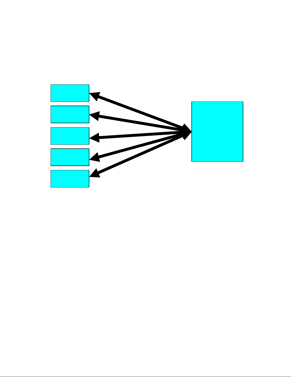
EVSE allows up to 5 MODBUS/TCP connections concurrently, which means that it allows 5
MODBUS/TCP clients devices to communicate with it at the same time assumed that each
MODBUS/TCP client device only open one connection.
The first client which connects to the MODBUS server will have command priority, meaning all of the
EVSE basic command functionality will be driven from this first client. Any additional client
connections will only have monitoring capabilities.
MODBUS/TCP
Client
MODBUS/TCP
Client
EVSE
MODBUS/TCP
Client
(MODBUS/TCP
Server)
MODBUS/TCP
Client
MODBUS/TCP
Client
EVSE supports 5 MODBUS/TCP communication connections
Figure – 3.3
GE WattStation Connect™ (a.k.a. GE Back end) server commands will take precedence over any
commands issued over the MODBUS protocol. BES will also have the capability to Enable/Disable the
MODBUS feature completely.
8 GE Energy ©2012 GE Company All Rights Reserved
Page 9

WattStationTM EV Charger MODBUS Register Guide
3.2 MODBUS Access Control
MODBUS protocol itself does not provide security feature. But in this architecture design, the EVSE
MODBUS communication application module adopts MODBUS access control based on the
MODBUS/TCP client IP address and access privilege. The authorized MODBUS/TCP clients and their
access privileges are set up through EVSE configuration.
MODBUS/TCP
Client IP Address
IP Address 1 Bit 0---Data Module 1
.
.
Bit 63---Data Module 64
Value of each bit of
0----read the corresponding
data module is not allowed.
1----read the corresponding
data module is allowed.
IP Address 2
IP Address 3
EVSE MODBUS/TCP messaging is just over TCP, not over SSL (Secure Socket Layer).
3.3 MODBUS Function Codes Supported
In this architecture design, all data MODBUS can access are mapped into the Holding registers, see
Chapter 20 for detail.
In the following descriptions, the MBAP header is omitted.
In this architecture design, EVSE supports the following function codes:
3.3.1 Function Code 3 (0x03): Read Holding Registers (Multiple)
Function code 0x03 is used to read the contents of a contiguous block of holding registers in EVSE.
The MODBUS Function code 0x03 Request PDU specifies the starting register address and the number
of registers to be read. In the PDU Registers are addressed starting at zero. Therefore registers
numbered 1-16 are addressed as 0-15.
Access Privilege
Read Write
Bit 0---Data Module 1
.
.
Bit 63---Data Module 64
Value of each bit of
0----read the corresponding data module
is not allowed.
1----read the corresponding data module
is allowed.
In this version, only Control Command
Module is designed for write.
MODBUS Access Control Table
Table – 3.1
9 GE Energy ©2012 GE Company All Rights Reserved
Page 10

WattStationTM EV Charger MODBUS Register Guide
MOODDBBUUSS FFCC 33 RReeqquueesstt
• M
Field Length (bytes) Value (hex)
Function Code 1 0x03
Starting Address 2 0x0000 to 0xFFFF
Number of Registers 2 0x1 to 0x7D (1 to 125)
Table – 3.2
The register data in the response message are packed as two bytes per register, with the binary
contents right justified within each byte.
For each register, the first byte contains the high order bits and the second contains
the low order bits.
• MODBUS FC 3 Response
Field Length (bytes) Value (hex)
Function Code 1 0x03
Byte Count 1 2 × N
Register Value 2 × N
Table – 3.3
Note: N is the number of registers specified in the request.
3.3.2 Function Code 4 (0x04): Read Input registers (multiple)
Function code 4 is used to read the contents of a contiguous block of input registers (read only) in
EVSE. The MODBUS Function code 4 Request PDU specifies the starting register address and the
number of registers to be read. In the PDU Registers are addressed starting at zero. Therefore
registers numbered 1-16 are addressed as 0-15.
• MODBUS FC 4 Request
Field Length (bytes) Value (hex)
Function Code 1 0x04
Starting Address 2 0x0000 to 0xFFFF
Number of Registers 2 0x1 to 0x7D (1 to 125)
Table – 3.4
The register data in the response message are packed as two bytes per register, with the binary
contents right justified within each byte. For each register, the first byte contains the high order bits
and the second contains the low order bits.
10 GE Energy ©2012 GE Company All Rights Reserved
Page 11

WattStationTM EV Charger MODBUS Register Guide
MOODDBBUUSS FFCC 44 RReessppoonnssee
MOODDBBUUSS FFCC 66 RReessppoonnssee
• M
(note N = Quantity of input registers)
Field Length (bytes) Value (hex)
Function Code 1 0x04
Byte Count 1 2 × N
Register Value 2 × N
3.3.3 Function Code 6 (0x06): Write single register
Table – 3.5
Function code 6 is used to write a single holding register in EVSE. The MODBUS Function code 6
Request PDU specifies the address if the register to be written. In the PDU Registers are addressed
starting at zero. Therefore registers numbered 1 is addressed as 0.
MODBUS FC 6 Request
Field Length (bytes) Value (hex)
Function Code 1 0x06
Register Address 2 0x0000 to 0xFFFF
Register Value 2 0x0000 to 0xFFFF
Table – 3.6
The register data in the response message are packed as two bytes per register, with the binary
contents right justified within each byte. For each register, the first byte contains the high order bits
and the second contains the low order bits.
• M
Field Length (bytes) Value (hex)
Function Code 1 0x06
Register Address 2 0x0000 to 0xFFFF
3.3.4 Function Code 16 (0x10): Write Multiple Holding Registers
Register Value 2 0x0000 to 0xFFFF
Table – 3.7
Function code 16 (0x10) is used to write data into a contiguous block of holding registers in EVSE.
The MODBUS Function code 16 (0x10) Request PDU specifies the starting register address, the number
of registers to be written, the data length, and the data values. In the PDU Registers are addressed
starting at zero. Therefore registers numbered 1-16 are addressed as 0-15.
11 GE Energy ©2012 GE Company All Rights Reserved
Page 12

WattStationTM EV Charger MODBUS Register Guide
• MODBUS FC 16 Request
(note N = quantity of registers to write to)
Field Length (bytes) Value (hex)
Function Code 1 0x10
Starting Address 2 0x0000 to 0xFFFF
Number of Registers 2 0x0001 to 0x7B (1 to 123)
Byte Count 1 2 × N
Registers Value N × 2 Value
Table – 3.8
The Normal MODBUS function code 16 (0x10) Response PDU specifies the starting register address
and the number of registers to be written.
• MODBUS FC 16 Response
Field Length (bytes) Value (hex)
Function Code 1 0x10
Starting Address 2 0x0000 to 0xFFFF
Quantity of Registers 2 0x0000 to 0x7B (1 to 123)
Table – 3.9
3.3.5 Function Code 23 (0x17): Read and Write Holding Registers
Function code 23 (0x17) performs a combination of one read operation and one write operation in a
single MODBUS transaction. The write operation is performed before the read.
The MODBUS Function code 23 (0x17) Request PDU specifies the read starting register address, the
number of registers to be read, the write starting register address, the number of registers to be
written, the write data length, and the write data values. In the PDU Registers are addressed starting
at zero. Therefore registers numbered 1-16 are addressed as 0-15.
• MODBUS FC 23 Request (note N = Quantity of registers to Write)
Field Length (bytes) Value (hex)
Function Code 1 0x17
Read Starting Address 1 0x0000 to 0xFFFF
Number of Registers to Read 2 0x0001 to 0x7D (1 to 125)
Write Starting Address 2 0x0000 to 0xFFFF
Number of Registers to Write 2 0x0001 to 0x79 (1 to 121)
Write Byte Count 1 2 × N
Write Registers Value N × 2 Value
Table – 3.10
12 GE Energy ©2012 GE Company All Rights Reserved
Page 13

WattStationTM EV Charger MODBUS Register Guide
The function code received in the MODBUS
The data address received in the MODBUS
The data address received in the MODBUS
Write request is not an allowable value for
the
The Normal MODBUS function code 23 Response PDU contains the data from the group of registers
that were read. The byte count field specifies the quantity of bytes to follow in the read data field.
• MODBUS FC 23 Response
Field Length (bytes) Value (hex)
Function Code 1 0x17
Read Byte Count 1 2 × N
Read Registers Value N × 2 Value
3.4 MODBUS Exception Codes Supported
In this version architecture design, the MODBUS in EVSE supports the following Exception Codes as
shown in following table.
Exception Code Exception Code Name Description
1 Illegal Function Code
2 Illegal Data Address
(N = Quantity of registers to Read)
Table – 3.11
request is not an allowable action in EVSE.
request is not an allowable address in EVSE.
3 Illegal Data Value
4 Slave Device Failure An unrecoverable error occurred when
Table – 3.12
• MMOODDBBUUSS EExxcceeppttiioonn RReessppoonnssee
Field Length (bytes) Value (hex)
Function Code 1 0x80 | Function Code
Exception Code 2 1-6
Table – 3.13
EVSE.
server (or the slave) was attempting to perform
the requested action.
(or pure addition operation)
13 GE Energy ©2012 GE Company All Rights Reserved
Page 14

WattStationTM EV Charger MODBUS Register Guide
0xx00000011
Moodduullee IIDD
0xx00
3.5 MODBUS Operations
3.5.1 Read EVSE MODBUS Register Data Module Info
In this architecture design, the authorized master device can get the MODBUS Register Data Module
information which includes the ID, address offset, and length of the data module w/ Function Code 3.
3.5.2 Read EVSE MODBUS Register Data
The authorized master device can read any valid MODBUS registers using Function code 3 or 23 as
shown in section 3.3.
3.5.3 Control EVSE
In this architecture design, the authorized master device can issue MODBUS Control command to
control EVSE by writing an appropriate value to the corresponding command register using function
code 16 or 23.
The supported
4.2.
MODBUS Control commands are defined and mapped to MODBUS registers in section
4 EVSE MODBUS Register Map
4.1 EVSE MODBUS Register Data Module Information Registers
EVSE Module Register Data Module
• Version of MODBUS Register Map.
• Number of MODBUS Data Register Modules in this version of MODBUS Register
Map.
• Data Module ID, Address Offset, and length of each module in the MODBUS
Register Map.
The address offset for EVSE Module Register Data Module
is defined as 0
MODBUS Data Model: Input registers (Read only)
The M
Address
(hex)
in this version of MODBUS Register Map.
for EVSE Module Register Data Module Information Registers is defined as 0
MODBUS
Register
Information Registers are designed to provide the information on
Information Registers
.
Variable
Name
Data
Range
Description Properties
(decimal)
Offset 1 MODBUS
Register
Data Module
Information
Registers
Validity
Offset+1 2 MODBUS >= Indicate the version of
0-1 Indicates whether the
values in the MODBUS
Data Module Information
Registers are valid or not.
0---Invalid
1---Valid
R
R
14 GE Energy ©2012 GE Company All Rights Reserved
Page 15

WattStationTM EV Charger MODBUS Register Guide
Data Module
Offset+2 3 MODBUS
Offset+3 4 Number of
Offset+4 5 Data Module
Offset+5 6 Data Module
Offset+6 7 Data Module
… … … … …
Offset+2+3×N 2+3×N Data Module
Offset+3+3×N 3+3×N Data Module
Offset+4+3×N 4+3×N Data Module
EVSE MODBUS Register Data Module Information Registers
Information
Map Version
Register
Registers
Version
Register
MODBUS
Register
Data
Modules
1 ID
1 Offset
1 Length
N ID
N Offset
N Length
Table - 4.1
0x1000 EVSE MODBUS Data
Module Information
Register
High byte ---- main
version.
Low byte ---- minor
version.
The current version of
EVSE MODBUS Data
Module Information
Register is 1.0.
>=
0x1000
1-65535 The number of data
Indicate the ID of Data
0x0000-
0xFFFF
Indicate the number of
Indicate the ID of Data
0x0000-
0xFFFF
Indicate the number of
Indicate the version of
EVSE MODBUS Register
Map
High byte ---- main
version.
Low byte ---- minor
version.
The current version of
EVSE MODBUS Register
Map is 1.0.
modules defined in the
current version of EVSE
MODBUS Register Map,
including this data
module.
Module 1.
Indicate the Address
offset of Data Module 1.
MODBUS Registers in the
data module 1.
Module N.
Indicate the Address
offset of Data Module N.
MODBUS Registers in the
data module N.
R
R
R
R
R
…
R
R
R
15 GE Energy ©2012 GE Company All Rights Reserved
Page 16

WattStationTM EV Charger MODBUS Register Guide
0xx001122DD ((330011ddeecciimmaall
MOODDBBUUSS DDaattaa MMooddeell
0xx11
4.2 EVSE MODBUS Operation Status Registers
Address
(hex)
MODBUS
Register
Variable
Name
(decimal)
Offset 301 EVSE
Operation
Status
Register
Validity
Offset+1 302 EVSE
0x1000 Indicate the version of EVSE
Operation
Status
Register
Version
Offset +
2
Offset +
3
Offset +
4
Offset +
5
EVSE Operation Status Register is used to give the user a quick and big picture
on the current EVSE operation status.
The address offset for EVSE Operation Status Register is defined as 0
nnoottaattiioonn)) in this version of MODBUS Register Map
M
The Module ID for EVSE Operation Status Registers is defined as 0
303 EVSE
Faulted
304 EV
Connected
305 EV
Charging
306 EVSE
Mode
: Input registers (Read only)
MODBUS Operation Status Registers
Data
Description Properties
Range
0-1 Indicates whether the values
in the EVSE Operation Status
Registers are valid or not.
0---Invalid
1---Valid
Operation Status Register
High byte ---- main version.
Low byte ---- minor version.
The current version of EVSE
Operation Status Register is
1.0.
0-1 EVSE faulted state
0—Not Faulted
1—EVSE Faulted
0-1 EV Connected state
0—No EV connected
1—EV Connected
0-1 EV Charging state
0—EV not charging
1—EV Charging
0-2 EVSE Mode of operation
0-Unknown Mode
1-Online
2- Offline
3- Online Auth. Disabled
4-Reserved
5-Configuration mode
6- Update mode
.
Table – 4.2
R
R
R
R
R
R
16 GE Energy ©2012 GE Company All Rights Reserved
Page 17

WattStationTM EV Charger MODBUS Register Guide
0xx00114411 ((332211 ddeecciimmaall nnoottaattiioonn))
0xx22
Register is 1.0.
4.3 EVSE Identification Register
EVSE Identification Register is used to give the user a quick and big picture on what features the
current EVSE supports.
The address offset for EVSE Identification Register is defined as 0
in this version of MODBUS Register Map.
MODBUS Data Model: Input registers (Read only)
The Module ID for EVSE Identification Registers is defined as 0
Address
(hex)
Offset 321 EVSE
Offset+1 322 EVSE
MODBUS
Register
(decimal)
Parameter Data
Identification
Register
Validity
Identification
Register
Version
Description Properties
Range
0-1 Indicates whether
the values in the
EVSE Identification
Registers are valid
or not.
0---Invalid
1---Valid
0x1000 Indicate the version
of EVSE
Identification
Register
High byte ---- main
version.
Low byte ---- minor
version.
The current version
of EVSE
Identification
R
R
17 GE Energy ©2012 GE Company All Rights Reserved
Offset+2+15 323+15 EVSE
15 ASCII
Identification
Register—
Station ID
EVSE Identification Registers
characters
Table – 4.3
EVSE Station unique
identifier
R
Page 18

WattStationTM EV Charger MODBUS Register Guide
addddrreessss ooffffsseett
Moodduullee IIDD
Register is 1.0.
4.4 EVSE Current Charging Information Diagnostic Registers
EEVVSSEE CCuurrrreenntt CChhaarrggiinngg IInnffoorrmmaattiioonn RReeggiisstteerrss provide the user information about the current
charging being performed.
The a
ddeecciimmaall nnoottaattiioonn)) in this version of MODBUS Register Map.
MMOODDBBUUSS DDaattaa MMooddeell: Input registers (Read only)
The M
Address
(hex)
Offset 341 Current
Offset+1 342 Current
MODBUS
Register
(decimal)
for EVSE current Charging Information registers is defined as 00xx00115555 ((334411 iinn
for EVSE last Charging Information registers is defined as 00xx33.
Parameter Data
Charging
Information
Registers
Validity
Charging
Information
Registers
Version
Description Properties
Range
0-1 This field indicates
whether the current
charging Registers
information are valid
or not.
0----Invalid
1----Valid
0x1000 Indicate the version
of EVSE Current
Charging Information
Register
High byte ---- main
version.
Low byte ---- minor
version.
The current version
of EVSE Current
Charging Information
R
R
18 GE Energy ©2012 GE Company All Rights Reserved
Offset+2 343 Current
Offset + 3 344 Temperature -100-
Offset + 4 345 Current 0-500A Current being
Offset+5 346 Current
Offset+6 347 Current 0-300V R
Charging
Status
Charging
Maximum
Current
0-1 This field indicates
whether EVSE
charging or not.
0----No Current
Charging
1----Current
Charging
The temperature
100C
6current
rating
inside the
WattStation
supplied to EV
Maximum current
allowed to send to EV
R
R
R
Page 19

WattStationTM EV Charger MODBUS Register Guide
Charging
Voltage
Offset+7 348 Current
Charging
Consumed
Power (high
16 bit)
Offset+8 349 Current
Charging
Consumed
Power(low 16
bit)
Offset+9 350 Current
Charging
Consumed
Energy(high
16 bit)
Offset+A 351 Current
Charging
Consumed
Energy(low 16
bit)
Offset+B 352 Current
Charging
time--seconds(high
16 bit)
Offset+C 353 Current
Charging
time--seconds(low
16 bit)
Offset+D 354 Connected
time--seconds(high
16 bit)
Offset+E 355 Connected
time--seconds(low
16 bit)
Current Charging Information Diagnostic Registers
065535
065535
065535
065535
065535
065535
065535
065535
Table – 4.4
The high 16 bit
values of the current
charging consumed
power.
The low 16 bit values
of the current
charging consumed
power.
The unit of power is
in Watt.
The high 16 bit
values of the current
charging consumed
energy.
The low 16 bit values
of the current
charging consumed
energy.
The unit of energy is
in Watt Hour.
The high 16 bit
values of Number of
seconds EV has been
charging
The low 16 bit values
of Number of
seconds EV has been
charging
The high 16 bit
values of Number of
seconds EV has been
connected
The low 16 bit values
of Number of
seconds EV has been
connected
R
R
R
R
R
R
R
R
19 GE Energy ©2012 GE Company All Rights Reserved
Page 20

WattStationTM EV Charger MODBUS Register Guide
0xx0011FF55
0xx44
Register is 1.0.
4.5 EVSE MODBUS Diagnostic Registers
EVSE SNTP Diagnostics Registers
The address offset for EVSE MODBUS Diagnostics registers is defined as 0
notation) in this version of MODBUS Register Map.
MODBUS Data Model: Input registers (Read only)
The Module ID for EVSE MODBUS Diagnostics registers is defined as 0
Address
(hex)
Offset 501 EVSE MODBUS
Offset+1 502 EVSE MODBUS
MODBUS
Register
(dec)
allow the user to view the EVSE MODBUS Diagnostics
Parameter Data
Diagnostic
Register Validity
Diagnostic
Register Version
.
Description Properties
Range
Indicate if the
MODBUS
Diagnostics
register is valid or
not.
0----Invalid
1----Valid
0x1000 High byte ----
main version.
Low byte ---minor version.
The current
version of EVSE
MODBUS
Diagnostics
data.
(501 in Decimal
R
R
Offset+2 503 MODBUS Service
Offset+3 504 MB Version
Offset+4 505 Maximum
Offset+5 506 Number of
Offset+6 507 Number of
Offset+7 508 Number of 0- R
20 GE Energy ©2012 GE Company All Rights Reserved
Feature Selected
Application
Version
Number MODBUS
Connections
MODBUS
Requests
Received
Bytes 3 and 2
MODBUS
Requests
Received
Bytes 1 and 0
0-2 0- Disabled
1- Basic function
2- Full function
R
R
R
065535
R
R
Page 21

WattStationTM EV Charger MODBUS Register Guide
0xx00225599
0xx55..
Register is 1.0.
MODBUS
Responses Sent
Bytes 3 and 2
Offset+8 509 Number of
MODBUS
Responses Sent
Bytes 1 and 0
Offset+9 510 Number of
MODBUS
Exceptions Sent
from the
Application
EVSE MODBUS Diagnostic Registers
4.6 EVSE MODBUS Connection Table Diagnostic Registers
EVSE MODBUS Connection Table Diagnostics Registers
Connection Table Diagnostics
The address offset for EVSE MODBUS Connection Table Diagnostics registers is defined as 0
(601 in decimal notation) in this version of MODBUS Register Map.
MODBUS Data Model: Input registers (Read only)
The Module ID for EVSE MODBUS Connection Table Diagnostics registers is defined as 0
Address
(hex)
Offset 601 MODBUS
Offset+1 602 MODBUS
MODBUS
Register
(dec)
data.
Parameter Data
Connection Table
Diagnostic
Register Validity
Connection Table
Diagnostic
Register Version
65535
065535
065535
Table – 4.5
Range
Indicate if the
0x1000 High byte ----
R
R
allow the user to view the EVSE MODBUS
Description Properties
R
MODBUS
Connection Table
Diagnostics
register is valid or
not.
0----Invalid
1----Valid
R
main version.
Low byte ---minor version.
The current
version of EVSE
MODBUS
Connection Table
Diagnostics
Offset+2 603 Client Connection
21 GE Energy ©2012 GE Company All Rights Reserved
1 Active
Indicate if
connection 1 is a
R
Page 22

WattStationTM EV Charger MODBUS Register Guide
Offset+3 604 Remote IP
Address
Bytes 3 and 2
Offset+4 605 Remote IP
Address
Bytes 1 and 0
Offset+5 606 Remote Port
Number
EVSE MODBUS Connection Table Diagnostic Registers
Remote MODBUS
065535
Remote MODBUS
Table – 4.6
currently opened
connection or not.
0----NOT
1----YES
R
Client IP address.
R
R
Client TCP port
number.
22 GE Energy ©2012 GE Company All Rights Reserved
Page 23

WattStationTM EV Charger MODBUS Register Guide
4.7 Summary of EVSE MODBUS Data Registers
Data Module Name Data Module ID MODBUS Address Offset
MODBUS Reg. Data Info. 0x0 0x0000
EVSE Op. Status Reg. 0x1 0x012D
EVSE ID Reg. 0x2 0x0141
Current charging info Reg. 0x3 0x0155
EVSE MODBUS Diag. Reg. 0x4 0x01F5
MODBUS connection
table Diag.
0x6
0x7
0x8
0x9
0xA
0xB
0xC
0xD
0xE
0xF
0x10
0x11
0x12
0x13
0x14
0x15
0x16
0x17
0x18
0x19
0x1A
0x5 0x0259
HEX
(DEC)
(0)
(301)
(321)
(341)
(501)
(601)
Table – 4.7
23 GE Energy ©2012 GE Company All Rights Reserved
Page 24

WattStationTM EV Charger MODBUS Register Guide
The instructions do not purport to cover all details or variations in equipment nor to provide for every
possible contingency to be met in connection with installation, operation or maintenance. Should
further information be desired or should particular problems arise which are not covered sufficiently
for the purchaser’s purposes, the matter should be referred to the GE Company.
24 GE Energy ©2012 GE Company All Rights Reserved
Page 25

GE Industrial Solutions
41 Woodford Ave.
Plainville, CT 06062
www.geindustrial.com
WattStationTM is a trademark of General Electric Company.
Information provided is subject to change without notice. Please verify all details with GE. All
Values are design or typical values when measured under laboratory conditions and GE makes
no warranty or guarantee, express or implied, that such performance will be obtained under enduse conditions.
DEH-41581A (4/12)
 Loading...