

Page 1
GE
Datasheet
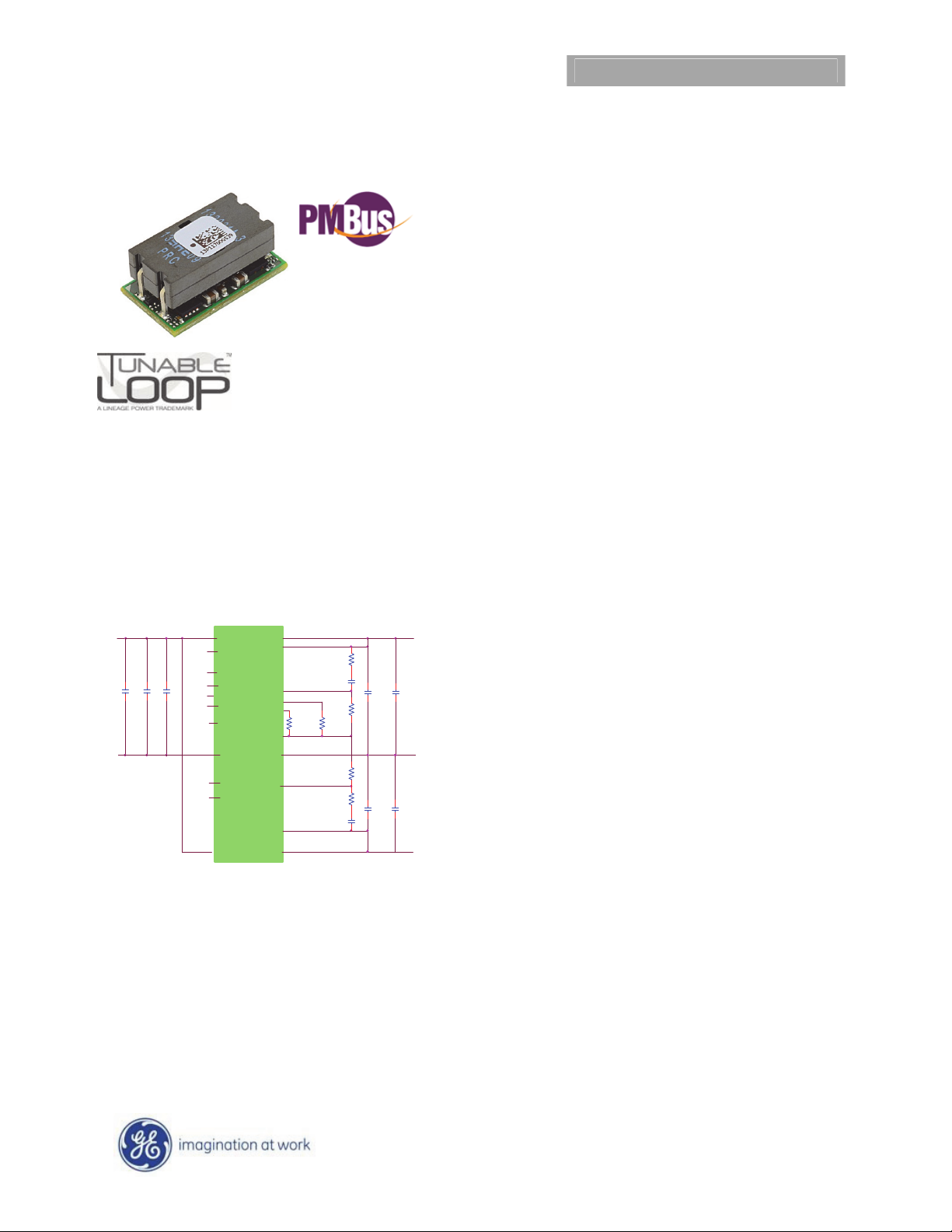
2 × 12A Digital Dual Output MicroDLynxTM: Non-Isolated DC-DC Power
Modules
4.5Vdc –14.4Vdc input; 0.51Vdc to 5.5Vdc output; 2 × 12A Output Current
Features
Wide Input voltage range (4.5Vdc-14.4Vdc)
Each Output voltage programmable from 0.6Vdc to
5.5Vdc via external resistor. Digitally adjustable down
to 0.51Vdc
Small size: 20.32 mm x 11.43 mm x 8.5 mm
(0.8 in x 0.45 in x 0.335 in)
RoHS Compliant
Applications
Distributed power architectures
Intermediate bus voltage applications
Telecommunications equipment
Servers and storage applications
Networking equipment
Industrial equipment
Vin+
CI2
CI3
CI1
GND
VIN1
PGOO D1
MODULE
SYNC
CLK
DA TA
SMBALRT#
ON/OFF1
PGND
ON/OFF2
PGOO D2
VIN2
VOUT1
VS+1
TRIM1
ADDR0
ADDR1
SIG_GND
PGND
TRIM2
VS+2
VOUT2
RADDR1
RTUNE1
CTUNE2
RTrim1
RADDR0
RTrim2
RTUNE2
CTUNE2
Vout+
CO1
CO3
CO2
CO4
Description
The 2 × 12A Digital Dual MicroDlynxTM power modules are non-isolated dc-dc converters that can deliver up to 2 × 12A of output
current. These modules operate over a wide range of input voltage (V
voltages from 0.51Vdc to 5.5Vdc, programmable via an external resistor and PMBus control. Features include a digital interface
using the PMBus protocol, remote On/Off, adjustable output voltage, over current and over temperature protection. The PMBus
interface supports a range of commands to both control and monitor the module. The module also includes the Tunable Loop
feature that allows the user to optimize the dynamic response of the converter to match the load with reduced amount of output
capacitance leading to savings on cost and PWB area.
*
UL is a registered trademark of Underwriters Laboratories, Inc.
†
CSA is a registered trademark of Canadian Standards Association.
‡
VDE is a trademark of Verband Deutscher Elektrotechniker e.V.
** ISO is a registered trademark of the International Organization of Standards
#
The PMBus name and logo are registered trademarks of the System Management Interface Forum (SMIF)
Wide operating temperature range -40°C to 85°C
TM #
Digital interface through the PMBus
Tunable Loop
TM
to optimize dynamic output voltage
protocol
response
Power Good signal for each output
Fixed switching frequency with capability of external
synchronization
180° Out-of-phase to reduce input ripple
Output overcurrent protection (non-latching)
Output Overvoltage protection
Over temperature protection
Remote On/Off
Ability to sink and source current
Start up into Pre-biased output
Cost efficient open frame design
Compliant to RoHS II EU “Directive 2011/65/EU”
Compatible in a Pb-free or SnPb reflow environment
Compliant to REACH Directive (EC) No 1907/2006
Compliant to IPC-9592 (September 2008), Category 2,
Class II
UL* 60950-1 2
60950-1-07 Certified, and VDE
nd
Ed. Recognized, CSA† C22.2 No.
‡
(EN60950-1 2nd Ed.)
Licensed
ISO** 9001 and ISO 14001 certified manufacturing
facilities
= 4.5Vdc-14.4Vdc) and provide precisely regulated output
IN
TM
February 14, 2014 ©2014 General Electric Corporation. All rights reserved.
Page 2
GE
Datasheet
2 × 12A Digital Dual MicroDlynxTM: Non-Isolated DC-DC Power Modules
4.5Vdc –14.4Vdc input; 0.51Vdc to 5.5Vdc output; 2 × 12A Output Current
Absolute Maximum Ratings
Stresses in excess of the absolute maximum ratings can cause permanent damage to the device. These are absolute stress
ratings only, functional operation of the device is not implied at these or any other conditions in excess of those given in the
operations sections of the data sheet. Exposure to absolute maximum ratings for extended periods can adversely affect the
device reliability.
Parameter Device Symbol Min Max Unit
Input Voltage All V
Continuous
VS+1, VS+2, SMBALERT# All -0.3 7 V
CLK, DATA, SYNC, All -0.3 3.6 V
Operating Ambient Temperature All T
(see Thermal Considerations section)
Storage Temperature All T
Electrical Specifications
Unless otherwise indicated, specifications apply over all operating input voltage, resistive load, and temperature conditions.
Parameter Device Symbol Min Typ Max Unit
Operating Input Voltage All
Maximum Input Current All
(VIN=3V to 14.4V, IO=I
Input No Load Current
= 12Vdc, IO = 0, module enabled)
(V
IN
Input Stand-by Current
= 12Vdc, module disabled)
(V
IN
Inrush Transient All I
Input Reflected Ripple Current, peak-to-peak
(5Hz to 20MHz, 1H source impedance; V
I
= I
; See Test Configurations)
O
Omax
Input Ripple Rejection (120Hz) All
)
O, max
V
= 0.6 Vdc
O,set
V
= 5.5Vdc
O,set
All
=4.5 to 14V,
IN
All
and V
IN1
IN2
A
stg
and
V
IN1
V
IN2
I
IN1,max &
I
IN2,max
I
IN1,No load &
I
IN2,No load
I
IN,1No load &
I
IN2,No load
I
IN1,stand-by &
I
IN2,stand-by
2
2
t & I
t 1 A2s
1
2
Both
Inputs
Both
Inputs
-0.3 15 V
-40 85 °C
-55 125 °C
4.5
⎯
23 Adc
72 mA
210 mA
14 mA
25 mAp-p
-68 dB
14.4 Vdc
February 14, 2014 ©2014 General Electric Corporation. All rights reserved. Page 2
Page 3
GE
Datasheet
2 × 12A Digital Dual MicroDlynxTM: Non-Isolated DC-DC Power Modules
4.5Vdc –14.4Vdc input; 0.51Vdc to 5.5Vdc output; 2 × 12A Output Current
Electrical Specifications (continued)
Parameter Device Symbol Min Typ Max Unit
Output Voltage Set-point (with 0.1% tolerance for external
resistor used to set output voltage)
Output Voltage (Over all operating input voltage, resistive load,
and temperature conditions until end of life)
All
All
Adjustment Range (selected by an external resistor)
(Some output voltages may not be possible depending on the
input voltage – see Feature Descriptions Section)
All VO1 & VO2 0.6* 5.5 Vdc
*0.51V possible through PMBus command
PMBus Adjustable Output Voltage Range All VO1,adj, VO2,adj -15 0 +10 %V
PMBus Output Voltage Adjustment Step Size All Both outputs 0.4 %V
Remote Sense Range All Both outputs 0.5 Vdc
Output Regulation (for VO 2.5Vdc) Both Outputs
Line (VIN=V
Load (IO=I
IN, min
O, min
to V
) All Both Outputs
IN, max
to I
) All Both Outputs
O, max
Output Regulation (for VO < 2.5Vdc)
Line (VIN=V
Load (IO=I
Temperature (T
IN, min
O, min
to V
) All Both Outputs
IN, max
to I
) All Both Outputs
O, max
to T
ref=TA, min
) All Both Outputs
A, max
Output Ripple and Noise on nominal output at 25°C
(VIN=V
output)
IN, nom
and IO=I
O, min
to I
Co = 2×0.1 + 2×47uF per
O, max
Peak-to-Peak (5Hz to 20MHz bandwidth) All
RMS (5Hz to 20MHz bandwidth) All 20 38 mV
External Capacitance1
Without the Tunable Loop
TM
ESR 1 m All C
With the Tunable Loop
TM
ESR 0.15 m All C
ESR 10 m All C
Output Current (in either sink or source mode) All I
Output Current Limit Inception (Hiccup Mode)
(current limit does not operate in sink mode)
All I
Output Short-Circuit Current All I
(VO250mV) ( Hiccup Mode )
Efficiency V
VIN= 12Vdc, TA=25°C V
IO=I
O, max , VO
= V
V
O,set
V
V
V
= 0.6Vdc 1, 2 79 %
O,set
= 1.2Vdc 1, 2 88 %
O, set
= 1.8Vdc 1, 2 91 %
O,set
= 2.5Vdc 1, 2 93 %
O,set
= 3.3Vdc 1, 2 94 %
O, set
= 5.0Vdc 1, 2 95 %
O,set
Switching Frequency All f
1
External capacitors may require using the new Tunable LoopTM feature to ensure that the module is stable as well as getting the best transient
response. See the Tunable Loop
TM
section for details.
VO1, set & VO2,
set
Vo1, set & VO2,
set
O, max
O, max
O, max
o
O, lim
, I
O1, s/c
O1, s/c
sw
-1.0 +1.0
-3.0
⎯
⎯
⎯
⎯
⎯
⎯
⎯
50 100 mV
+3.0
+0.4 % V
10 mV
5 mV
10 mV
0.4 % V
2×47
⎯
⎯
⎯
2×47 F
1000 F
5000 F
0 12x2 Adc
150 % I
6 Arms
500
⎯
⎯
% VO,
set
% VO,
set
O,set
O,set
O, set
O, set
pk-pk
rms
o,max
kHz
February 14, 2014 ©2014 General Electric Corporation. All rights reserved. Page 3
Page 4
GE
Datasheet
2 × 12A Digital Dual MicroDlynxTM: Non-Isolated DC-DC Power Modules
4.5Vdc –14.4Vdc input; 0.51Vdc to 5.5Vdc output; 2 × 12AOutput Current
Electrical Specifications (continued)
Parameter Device Symbol Min Typ Max Unit
Frequency Synchronization All
Synchronization Frequency Range All -20% +20% kHz
High-Level Input Voltage All VIH 2.0 V
Low-Level Input Voltage All VIL 0.4 V
Input Current, SYNC All ISYNC 100 nA
Minimum Pulse Width, SYNC All tSYNC 100 ns
Maximum SYNC rise time All tSYNC_SH 100 ns
General Specifications
Parameter Device Min Typ Max Unit
Calculated MTBF (IO=0.8I
Weight
, TA=40°C) Telecordia Issue 2 Method 1 Case 3 All 75,767,425 Hours
O, max
⎯
4.5 (0.16)
⎯
g (oz.)
Feature Specifications
Unless otherwise indicated, specifications apply over all operating input voltage, resistive load, and temperature conditions. See
Feature Descriptions for additional information.
Parameter Device Symbol Min Typ Max Unit
On/Off Signal Interface
(VIN=V
Signal referenced to GND)
Device Code with no suffix – Negative Logic (See Ordering Information)
(On/OFF pin is open collector/drain logic input with
external pull-up resistor; signal referenced to GND)
Logic High (Module OFF)
Input High Current All IIH1, IIH2 — — 1 mA
Input High Voltage All VIH1, VIH2 2 — V
Logic Low (Module ON)
Input low Current All IIL1, IIL2 — — 20 A
Input Low Voltage All VIL1, VIL2 -0.2 — 0.6 Vdc
Turn-On Delay and Rise Times
(VIN=V
Case 1: On/Off input is enabled and then input power is
applied (delay from instant at which V
10% of V
Case 2: Input power is applied for at least one second and
then the On/Off input is enabled (delay from instant at
which Von/Off is enabled until V
Output voltage Rise time (time for Vo to rise from
10% of Vo, set to 90% of Vo, set)
Output voltage overshoot (TA = 25oC
V
IN
With or without maximum external capacitance
= V
IN, min
IN, nom
IN, min
to V
, IO=I
o, set)
to V
; open collector or equivalent,
IN, max
to within ±1% of steady state)
O, max , VO
Tdelay1,
Tdelay2
Tdelay1,
Tdelay2
Trise2
Both
Outputs
— 2 — msec
— 800 —
— 5 — msec
3.0 % V
IN, max,IO
= V
until Vo =
IN
IN, min
o = 10% of Vo, set)
All
All
All Trise1,
= I
to I
O, min
O, max
)
Vdc
IN, max
μsec
O, set
February 14, 2014 ©2014 General Electric Corporation. All rights reserved. Page 4
Page 5

GE
Datasheet
2 × 12A Digital Dual MicroDlynxTM: Non-Isolated DC-DC Power Modules
4.5Vdc –14.4Vdc input; 0.51Vdc to 5.5Vdc output; 2 × 12A Output Current
Feature Specifications (cont.)
Parameter Device Symbol Min Typ Max Units
Over Temperature Protection
(See Thermal Considerations section)
PMBus Over Temperature Warning Threshold* All T
Input Undervoltage Lockout
All T
ref
WARN
Turn-on Threshold All Both Inputs 4.5 Vdc
Turn-off Threshold All Both Inputs
Hysteresis All Both Inputs
PMBus Adjustable Input Under Voltage Lockout Thresholds All Both Inputs
Resolution of Adjustable Input Under Voltage Threshold All Both Inputs
PGOOD (Power Good)
135 °C
125 °C
4.25 Vdc
0.15 0.2 Vdc
4 14 Vdc
250 mV
Signal Interface Open Drain, V
supply
≤ 5VDC
Overvoltage threshold for PGOOD ON All Both Outputs 108.33 %V
Overvoltage threshold for PGOOD OFF All Both Outputs
Undervoltage threshold for PGOOD ON All Both Outputs
Undervoltage threshold for PGOOD OFF All Both Outputs
Pulldown resistance of PGOOD pin All Both Outputs
Sink current capability into PGOOD pin All Both Outputs
112.5 %V
91.67 %V
87.5 %V
40 70
5 mA
* Over temperature Warning – Warning may not activate before alarm and unit may shutdown before warning
Ω
O, set
O, set
O, set
O, set
February 14, 2014 ©2014 General Electric Corporation. All rights reserved. Page 5
Page 6
GE
Datasheet
2 × 12A Digital Dual MicroDlynxTM: Non-Isolated DC-DC Power Modules
4.5Vdc –14.4Vdc input; 0.51Vdc to 5.5Vdc output; 2 × 12AOutput Current
Digital Interface Specifications
Unless otherwise indicated, specifications apply over all operating input voltage, resistive load, and temperature conditions. See
Feature Descriptions for additional information.
Parameter Conditions Symbol Min Typ Max Unit
PMBus Signal Interface Characteristics
Input High Voltage (CLK, DATA) VIH 2.1 V
Input Low Voltage (CLK, DATA) VIL 0.8 V
Input high level current (CLK, DATA) IIH -10 10 A
Input low level current (CLK, DATA) IIL -10 10 mA
Output Low Voltage (CLK, DATA, SMBALERT#) I
Output high level open drain leakage current (DATA,
SMBALERT#)
Pin capacitance CO 0 1 pF
PMBus Operating frequency range Slave Mode FPMB 10 400 kHz
Data hold time
Data setup time
Measurement System Characteristics
Output current measurement range
Output current measurement gain accuracy (at 25°C)
V
measurement range
OUT
V
measurement accuracy
OUT
=2mA VOL 0.4? V
OUT
V
=3.6V I
OUT
Receive Mode
Transmit Mode
tSU:DAT
OH
tHD:DAT
I
RNG
I
ACC
V
OUT(rng)
0 10 A
0
300
250 ns
0 18 A
±1 A
0.5 5.8 V
-2 2 %
ns
February 14, 2014 ©2014 General Electric Corporation. All rights reserved. Page 6
Page 7

,
GE
Datasheet
2 × 12A Digital Dual MicroDlynxTM: Non-Isolated DC-DC Power Modules
4.5Vdc –14.4Vdc input; 0.51Vdc to 5.5Vdc output; 2 × 12A Output Current
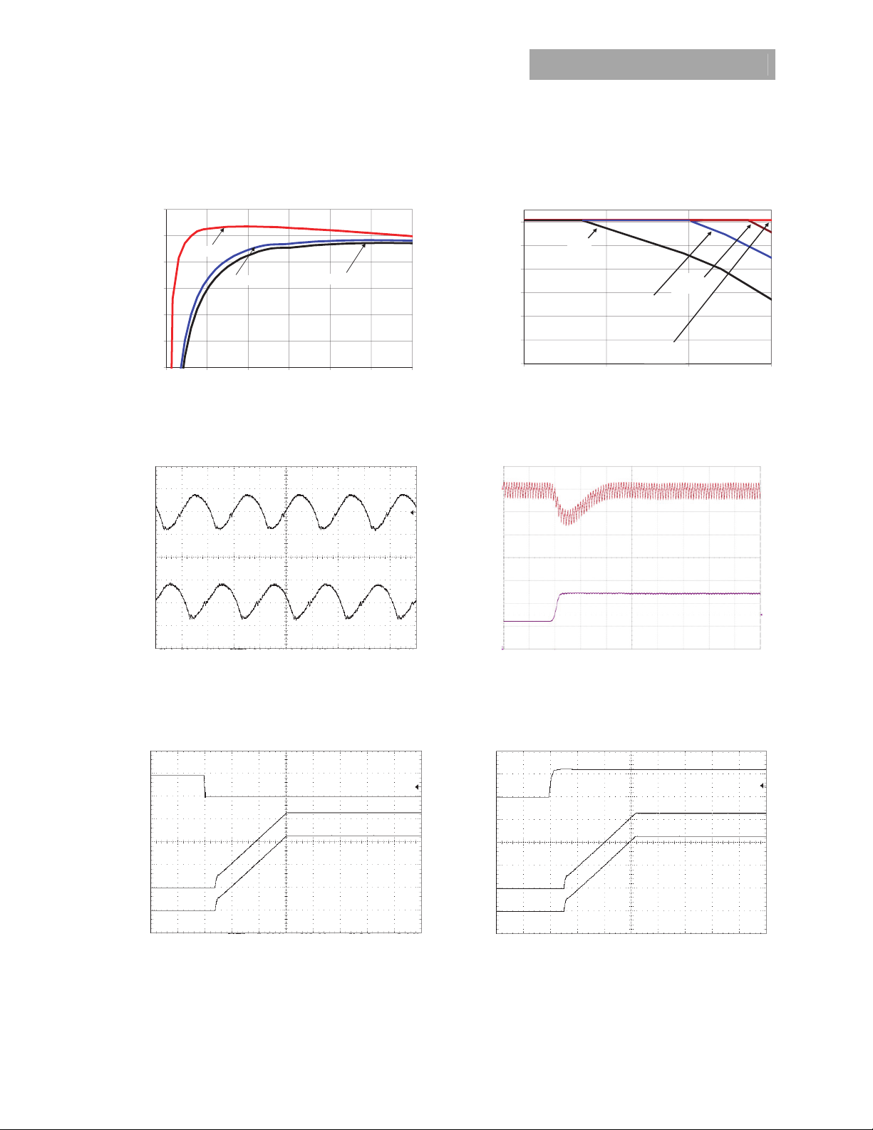
Characteristic Curves
The following figures provide typical characteristics for the 2 × 12A Digital Dual MicroDlynxTM at 0.6Vo and 25oC.
90
85
80
75
70
65
60
EFFICIENCY, η (%)
55
50
Vin=4.5V
Vin=12V
2x0 2x2 2x4 2x6 2x8 2x10 2x12
OUTPUT CURRENT, IO (A) AMBIENT TEMPERATURE, TA OC
Vin=14V
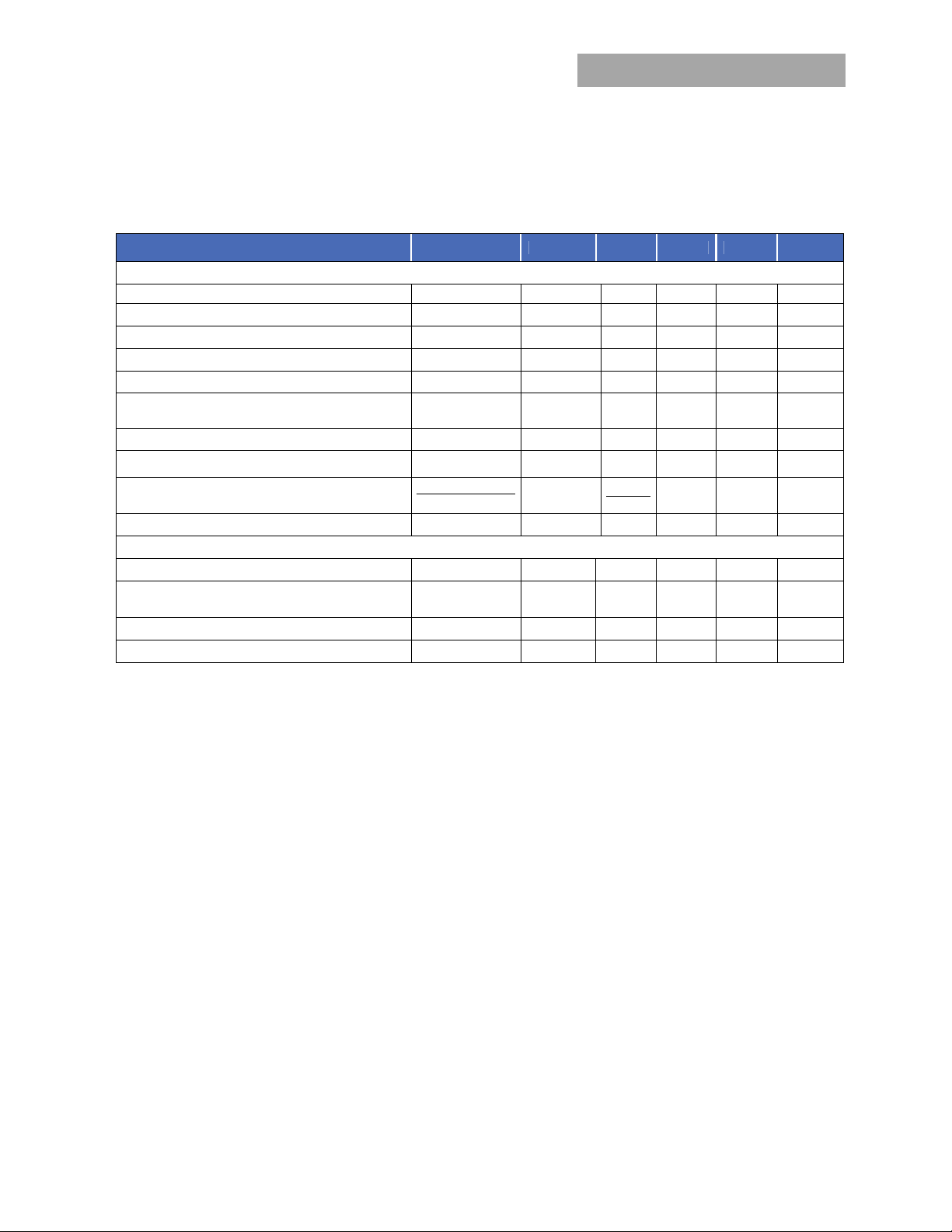
Figure 1. Converter Efficiency versus Output Current.
Figure 2. Derating Output Current versus Ambient
Temperature and Airflow.
12
Derating curve applies
10
to Both Outputs
8
6
4
2
OUTPUT CURRENT, Io (A)
0
55 60 65 70 75 80 85
(V) (30mV/div)
O
V
OUTPUT VOLTAGES
TIME, t (1μs/div) TIME, t (20μs /div)
Figure 3. Typical output ripple and noise (CO=
IN
2×0.1uF+2×47uF ceramic, V
(V) (5V/div)
ON/OFF
(V) (200mV/div) V
O
= 12V, Io = I
o1,max, Io2,max,
(20mV/div)
O
(A) (5Adiv) V
O
I
OUTPUT CURRENT, OUTPUT VOLTAGE
Figure 4. Transient Response to Dynamic Load Change from
).
50% to 100% on one output at 12Vin,
Cout=2x47uF+7x330uF
CTune=12nF, RTune=300
(V) (10V/div)
IN
(V) (200mV/div) V
O
OUTPUT VOLTAGES ON/OFF VOLTAGE
V
Figure 5. Typical Start-up Using On/Off Voltage (Vin=12V, Io=
o1,max, Io2,max,
I
).
TIME, t (2ms/div) TIME, t (2ms/div)
OUTPUT VOLTAGES INPUT VOLTAGE
V
Figure 6. Typical Start-up Using Input Voltage (V
o1,max, Io2,max,
I
).
IN
= 12V, Io=
February 14, 2014 ©2014 General Electric Corporation. All rights reserved. Page 7
Page 8
GE
Datasheet
2 × 12A Digital Dual MicroDlynxTM: Non-Isolated DC-DC Power Modules
4.5Vdc –14.4Vdc input; 0.51Vdc to 5.5Vdc output; 2 × 12AOutput Current
Characteristic Curves
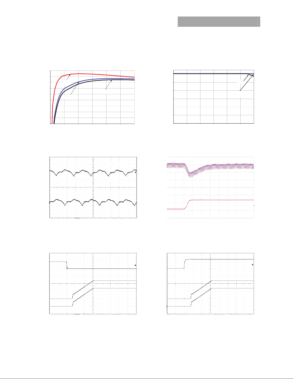
The following figures provide typical characteristics for the 2 × 12A Digital Dual MicroDlynxTM at 1.2Vo and 25oC.
95
90
85
80
75
70
65
60
EFFICIENCY, η (%)
55
50
Vin=4.5V
Vin=14V
Vin=12V
2x0 2x2 2x4 2x6 2x8 2x10 2x12
OUTPUT CURRENT, IO (A) AMBIENT TEMPERATURE, TA OC
Figure 7. Converter Efficiency versus Output Current.
Figure 8. Derating Output Current versus Ambient
Temperature and Airflow.
12
Derating curve applies
10
to Both Outputs
8
6
4
2
OUTPUT CURRENT, Io (A)
0
55 60 65 70 75 80 85
0.5m/s
(100LFM)
NC
(V) (30mV/div)
O
V
OUTPUT VOLTAGES
TIME, t (1μs/div) TIME, t (20μs /div)
Figure 9. Typical output ripple and noise (CO=
2×0.1uF+2×47uF ceramic, V
(V) (5V/div)
ON/OFF
(V) (500mV/div) V
O
IN
= 12V, Io = I
o1,max, Io2,max
(20mV/div)
O
(A) (5Adiv) V
O
I
OUTPUT CURRENT, OUTPUT VOLTAGE
Figure 10. Transient Response to Dynamic Load Change on
).
one output from 50% to 100% at 12Vin,
Cout=3x47uF+3x330uF, CTune=2700pF & RTune=300
(V) (10V/div)
IN
(V) (500mV/div) V
O
OUTPUT VOLTAGES ON/OFF VOLTAGE
V
Figure 1. Typical Start-up Using On/Off Voltage (VIN= 12V, I
= I
o1,max, Io2,max
).
TIME, t (2ms/div) TIME, t (2ms/div)
o
OUTPUT VOLTAGES INPUT VOLTAGE
V
Figure 12. Typical Start-up Using Input Voltage (V
I
o1,max, Io2,max
).
IN
= 12V, Io=
February 14, 2014 ©2014 General Electric Corporation. All rights reserved. Page 8
Page 9
t
GE
Datasheet
2 × 12A Digital Dual MicroDlynxTM: Non-Isolated DC-DC Power Modules
4.5Vdc –14.4Vdc input; 0.51Vdc to 5.5Vdc output; 2 × 12A Output Current
Characteristic Curves
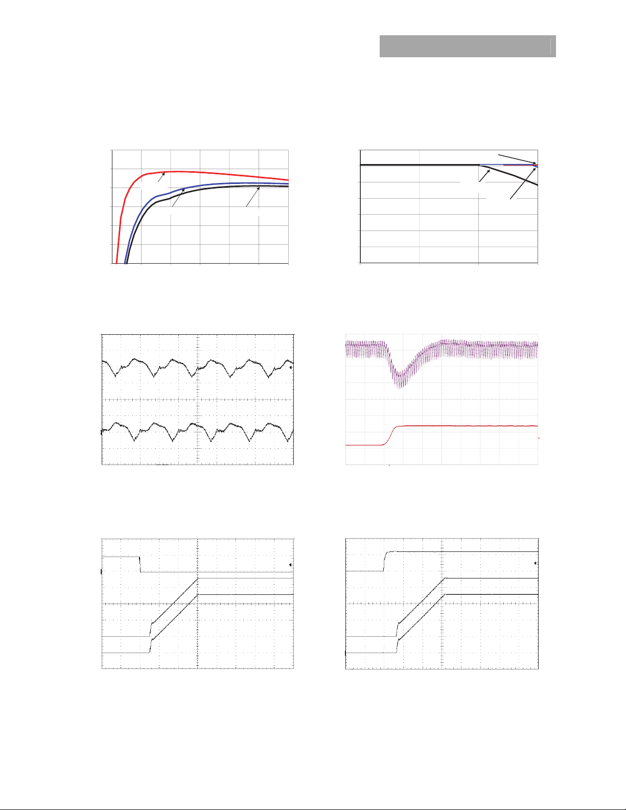
The following figures provide typical characteristics for the 2 × 12A Digital Dual MicroDlynxTM at 1.8Vo and 25oC.
100
95
90
85
80
EFFICIENCY, η (%)
75
70
2x0 2x2 2x4 2x6 2 x8 2x10 2x12
Vin=4.5V
Vin=12V
OUTPUT CURRENT, IO (A) AMBIENT TEMPERATURE, TA OC
Vin=14V
Figure 13. Converter Efficiency versus Output Current.
14
12
Derating curve applies
10
to Both Outputs
8
6
4
2
OUTPUT CURRENT, Io (A)
0
55 65 75 85
Figure 14. Derating Output Current versus Ambient
Temperature and Airflow.
1.0m/s
(200LFM)
NC
0.5m/s
(100LFM)
(V) (30mV/div)
O
V
OUTPUT VOLTAGES
TIME, t (1μs/div) TIME, t (20μs /div)
Figure 15. Typical output ripple and noise (CO=
IN
2×0.1uF+2×47uF ceramic, V
(V) (5V/div)
ON/OFF
(V) (500mV/div) V
O
= 12V, Io = I
o1,max, Io2,max
(20mV/div)
O
(A) (5Adiv) V
O
I
OUTPUT CURRENT, OUTPUT VOLTAGE
Figure 16. Transient Response to Dynamic Load Change on
).
one output from 50% to 100% at 12Vin, Cout =
3x47uF+2x330uF, CTune = 1800pF & RTune = 300
(V) (10V/div)
IN
(V) (500mV/div) V
O
OUTPUT VOLTAGES ON/OFF VOLTAGE
V
Figure 17. Typical Start-up Using On/Off Voltage (VIN= 12V, I
= I
o1,max, Io2,max
).
TIME, t (2ms/div) TIME, t (2ms/div)
OUTPUT VOLTAGES INPUT VOLTAGE
V
o
Figure 18. Typical Star
I
o1,max, Io2,max
).
-up Using Input Voltage (VIN= 12V, Io=
February 14, 2014 ©2014 General Electric Corporation. All rights reserved. Page 9
Page 10
t
GE
Datasheet
2 × 12A Digital Dual MicroDlynxTM: Non-Isolated DC-DC Power Modules
4.5Vdc –14.4Vdc input; 0.51Vdc to 5.5Vdc output; 2 × 12AOutput Current
Characteristic Curves
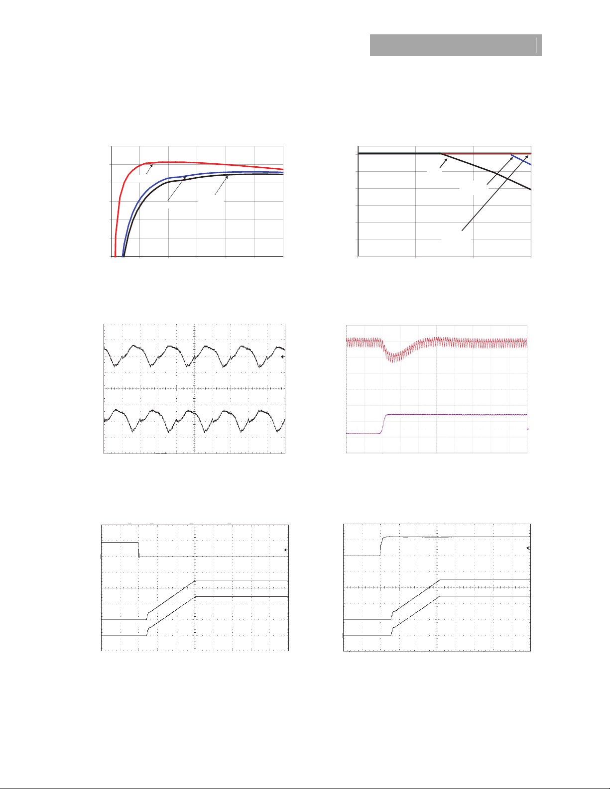
The following figures provide typical characteristics for the 2 × 12A Digital Dual MicroDlynxTM at 2.5Vo and 25oC.
100
95
90
85
80
EFFICIENCY, η (%)
75
70
Vin=4.5V
Vin=12V
2x0 2x2 2x4 2x6 2 x8 2x10 2x12
OUTPUT CURRENT, IO (A) AMBIENT TEMPERATURE, TA OC
Vin=14V
Figure 19. Converter Efficiency versus Output Current.
Figure 20. Derating Output Current versus Ambient
Temperature and Airflow.
12
10
Derating curve applies
8
to Both Outputs
6
4
2
OUTPUT CURRENT, Io (A)
0
55 65 75 85
NC
1m/s
(200LFM)
0.5m/s
(100LFM)
(V) (30mV/div)
O
V
OUTPUT VOLTAGES
TIME, t (1μs/div) TIME, t (20μs /div)
Figure 21. Typical output ripple and noise (CO=
2x0.1uF+2x47uF ceramic, V
(V) (5V/div)
ON/OFF
(V) (1V/div) V
O
IN
= 12V, Io = I
o1,max, Io2,max
(50mV/div)
O
(A) (5Adiv) V
O
I
OUTPUT CURRENT, OUTPUT VOLTAGE
Figure 22. Transient Response to Dynamic Load Change on
).
one output from 50% to 100% at 12Vin,
Cout=3x47uF+2x330uF, CTune=1500pF & RTune = 300
(V) (10V/div)
IN
(V) (1V/div) V
O
OUTPUT VOLTAGES ON/OFF VOLTAGE
V
Figure 23. Typical Start-up Using On/Off Voltage (VIN= 12V, I
= I
o1,max, Io2,max
).
TIME, t (2ms/div) TIME, t (2ms/div)
OUTPUT VOLTAGES INPUT VOLTAGE
V
o
Figure 24. Typical Star
I
o1,max, Io2,max
).
-up Using Input Voltage (VIN= 12V, Io=
February 14, 2014 ©2014 General Electric Corporation. All rights reserved. Page 10
Page 11
GE
Datasheet
2 × 12A Digital Dual MicroDlynxTM: Non-Isolated DC-DC Power Modules
4.5Vdc –14.4Vdc input; 0.51Vdc to 5.5Vdc output; 2 × 12A Output Current
Characteristic Curves
The following figures provide typical characteristics for the 2 × 12A Digital Dual MicroDlynxTM at 3.3Vo and 25oC.
100
95
Vin=4.5V
90
85
80
EFFICIENCY, η (%)
75
70
2x0 2x2 2x4 2x6 2 x8 2x10 2x12
Vin=12V
OUTPUT CURRENT, IO (A) AMBIENT TEMPERATURE, TA OC
Vin=14V
Figure 25. Converter Efficiency versus Output Current.
Figure 26. Derating Output Current versus Ambient
Temperature and Airflow.
12
10
Derating curve applies
8
to Both Outputs
6
4
2
OUTPUT CURRENT, Io (A)
0
55 65 75 85
NC
1m/s
(200LFM)
0.5m/s
(100LFM)
1.5m/s
(300LFM)
(V) (30mV/div)
O
V
OUTPUT VOLTAGES
TIME, t (1μs/div) TIME, t (20μs /div)
Figure 27. Typical output ripple and noise (CO=
IN
2x0.1uF+2x47uF ceramic, V
(V) (5V/div)
ON/OFF
(V) (1V/div) V
O
= 12V, Io = I
o1,max, Io2,max
(V) (50mV/div)
O
(A) (5Adiv) V
O
I
OUTPUT CURRENT, OUTPUT VOLTAGE
Figure 28 Transient Response to Dynamic Load Change on
).
one output from 50% to 100% at 12Vin,
Cout=3x47uF+1x330uF, CTune = 1200pF & RTune = 300
(V) (10V/div)
IN
(V) (1V/div) V
O
OUTPUT VOLTAGES ON/OFF VOLTAGE
V
Figure 29. Typical Start-up Using On/Off Voltage (VIN= 12V, I
= I
o1,max, Io2,max
).
TIME, t (2ms/div) TIME, t (2ms/div)
o
OUTPUT VOLTAGES INPUT VOLTAGE
V
Figure 30. Typical Start-up Using Input Voltage (V
I
o1,max, Io2,max
).
IN
= 12V, Io=
February 14, 2014 ©2014 General Electric Corporation. All rights reserved. Page 11
Page 12

GE
Datasheet
2 × 12A Digital Dual MicroDlynxTM: Non-Isolated DC-DC Power Modules
4.5Vdc –14.4Vdc input; 0.51Vdc to 5.5Vdc output; 2 × 12AOutput Current
Characteristic Curves
The following figures provide typical characteristics for the 2 × 12A Digital Dual MicroDlynxTM at 5Vo and 25oC.
100
95
90
85
80
EFFICIENCY, η (%)
75
70
Figure 31. Converter Efficiency versus Output Current.
Vin=7V
Vin=12V
2x0 2x2 2x4 2x6 2 x8 2x10 2x12
OUTPUT CURRENT, IO (A) AMBIENT TEMPERATURE, TA OC
Vin=14V
OUTPUT CURRENT, Io (A)
Figure 32. Derating Output Current versus Ambient
Temperature and Airflow.
(V) (30mV/div)
O
V
OUTPUT VOLTAGES
TIME, t (1μs/div) TIME, t (20μs /div)
Figure 33. Typical output ripple and noise (C
2×47uF ceramic, V
(V) (5V/div)
ON/OFF
(V) (2V/div) V
O
IN
= 12V, Io = I
o1,max, Io2,max
= 2×0.1uF +
O
).
(50mV/div)
O
(A) (5Adiv) V
O
I
OUTPUT CURRENT, OUTPUT VOLTAGE
Figure 34. Transient Response to Dynamic Load Change on
one output from 50% to 100% at 12Vin, Cout=6x47uF,
CTune=470pF & RTune=300
(V) (10V/div)
IN
(V) (2V/div) V
O
OUTPUT VOLTAGES ON/OFF VOLTAGE
V
Figure 35. Typical Start-up Using On/Off Voltage (VIN = 12V, Io
o1,max, Io2,max
= I
).
TIME, t (2ms/div) TIME, t (2ms/div)
OUTPUT VOLTAGES INPUT VOLTAGE
V
Figure 36. Typical Start-up Using Input Voltage (V
o1,max, Io2,max
I
).
IN
= 12V, Io =
February 14, 2014 ©2014 General Electric Corporation. All rights reserved. Page 12
Page 13

GE
Datasheet
2 × 12A Digital Dual MicroDlynxTM: Non-Isolated DC-DC Power Modules
4.5Vdc –14.4Vdc input; 0.51Vdc to 5.5Vdc output; 2 × 12A Output Current
Design Considerations
Input Filtering
The2 × 12A Digital Dual MicroDlynxTM module should be
connected to a low ac-impedance source. A highly
inductive source can affect the stability of the module. An
input capacitance must be placed directly adjacent to the
input pin of the module, to minimize input ripple voltage
and ensure module stability.
To minimize input voltage ripple, ceramic capacitors are
recommended at the input of the module. Figure 37
shows the input ripple voltage for various output voltages
at2 x 12A of load current with 2x22 µF or 3x22 µF ceramic
capacitors and an input of 12V.
200
150
100
Ripple (mVp-p)
50
0
0.511.522.533.544.55
Figure 37. Input ripple voltage for various output
voltages with 4x22 µF or 6x22 µF ceramic capacitors at
the input (2 x 12A load). Input voltage is 12V.
Output Filtering
These modules are designed for low output ripple voltage
and will meet the maximum output ripple specification with
0.1 µF ceramic and 22 µF ceramic capacitors at the output
of the module. However, additional output filtering may be
required by the system designer for a number of reasons.
First, there may be a need to further reduce the output
ripple and noise of the module. Second, the dynamic
response characteristics may need to be customized to a
particular load step change.
To reduce the output ripple and improve the dynamic
response to a step load change, additional capacitance at
the output can be used. Low ESR polymer and ceramic
capacitors are recommended to improve the dynamic
response of the module. Figure 38 provides output ripple
information for different external capacitance values at
various Vo and a full load current of2 x 12A. For stable
operation of the module, limit the capacitance to less than
the maximum output capacitance as specified in the
electrical specification table. Optimal performance of the
module can be achieved by using the Tunable Loop
feature described later in this data sheet.
4x22uF
6x22uF
Output Voltage(Volts)
TM
80
70
60
2x47uF each output
3x47uF each output
4x47uF each output
50
40
30
20
Ripple (mVp-p)
10
0
0.51.52.53.54.5
Output Voltage(Volts)
Figure 38. Output ripple voltage for various output
voltages with total external 4x47 µF, 6x47 µF or 8x47 µF
ceramic capacitors at the output (2 x 12A load). Input
voltage is 12V.
Safety Considerations
For safety agency approval the power module must be
installed in compliance with the spacing and separation
requirements of the end-use safety agency standards, i.e.,
UL 60950-1 2nd, CSA C22.2 No. 60950-1-07, DIN EN 609501:2006 + A11 (VDE0805 Teil 1 + A11):2009-11; EN 609501:2006 + A11:2009-03.
For the converter output to be considered meeting the
requirements of safety extra-low voltage (SELV), the input
must meet SELV requirements. The power module has
extra-low voltage (ELV) outputs when all inputs are ELV.
The input to these units is to be provided with a fast-acting
fuse with a maximum rating of 30A in the positive input
. (Littelfuse 456 Series or equivalent)
lead
February 14, 2014 ©2014 General Electric Corporation. All rights reserved. Page 13
Page 14

GE
Datasheet
2 × 12A Digital Dual MicroDlynxTM: Non-Isolated DC-DC Power Modules
4.5Vdc –14.4Vdc input; 0.51Vdc to 5.5Vdc output; 2 × 12AOutput Current
Analog Feature Descriptions
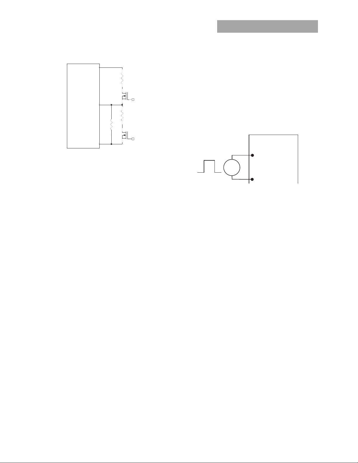
Remote On/Off
The module can be turned ON and OFF either by using the
ON/OFF pin (Analog interface) or through the PMBus
interface (Digital). The module can be configured in a
number of ways through the PMBus interface to react to the
two ON/OFF inputs:
• Module ON/OFF can be controlled only through
the analog interface (digital interface ON/OFF
commands are ignored)
• Module ON/OFF can be controlled only through
the PMBus interface (analog interface is ignored)
• Module ON/OFF can be controlled by either the
analog or digital interface
The default state of the module (as shipped from the factory)
is to be controlled by the analog interface only. If the digital
interface is to be enabled, or the module is to be controlled
only through the digital interface, this change must be made
through the PMBus. These changes can be made and
written to non-volatile memory on the module so that it is
remembered for subsequent use.
Analog On/Off
The2 × 12A Digital Dual MicroDlynxTM power modules
feature an On/Off pin for remote On/Off operation. Two
On/Off logic options are available. In the Positive Logic
On/Off option, (device code suffix “4” – see Ordering
Information), the module turns ON during a logic High on the
On/Off pin and turns OFF during a logic Low. With the
Negative Logic On/Off option, (no device code suffix, see
Ordering Information), the module turns OFF during logic
High and ON during logic Low. The On/Off signal should be
always referenced to ground. For either On/Off logic option,
leaving the On/Off pin disconnected will turn the module ON
when input voltage is present.
For positive logic modules, the circuit configuration for using
the On/Off pin is shown in Figure 39. For negative logic
On/Off modules, the circuit configuration is shown in Fig. 40.
Digital On/Off
Please see the Digital Feature Descriptions section.
TBD
Figure 39. Circuit configuration for using positive On/Off
logic.
Output 1
+VI N
DUAL OUTPUT MODULE
Rpullup
I
ON/OF F1
+
Q2
V
ON/OFF1
_
22K
GND
+3. 3V
47K
ENABLE1
Q1
22K
Output 2
+VI N
DUAL OUTPUT MODULE
Rpullup
I
ON/OF F2
+
Q2
V
ON/OFF2
_
22K
GND
+3. 3V
47K
ENABLE2
Q2
22K
Figure 40. Circuit configuration for using negative On/Off
logic.
Monotonic Start-up and Shutdown
The module has monotonic start-up and shutdown behavior
for any combination of rated input voltage, output current
and operating temperature range.
Startup into Pre-biased Output
The module can start into a prebiased output on either or
both outputs as long as the prebias voltage is 0.5V less than
the set output voltage.
Analog Output Voltage Programming
The output voltage of each output of the module shall be
programmable to any voltage from 0.6dc to 5.5Vdc by
connecting a resistor between the 2 Trims and SIG_GND
pins of the module. Certain restrictions apply on the output
voltage set point depending on the input voltage. These are
shown in the Output Voltage vs. Input Voltage Set Point Area
plot in Fig. 1. The Upper Limit curve shows that for output
voltages lower than 1V, the input voltage must be lower
than the maximum of 14.4V. If the module can operate at
14.4V below 1V then that is preferable over the existing
upper curve. The Lower Limit curve shows that for output
voltages higher than 0.6V, the input voltage needs to be
larger than the minimum of 4.5V.
February 14, 2014 ©2014 General Electric Corporation. All rights reserved. Page 14
Page 15

GE
Datasheet
2 × 12A Digital Dual MicroDlynxTM: Non-Isolated DC-DC Power Modules
4.5Vdc –14.4Vdc input; 0.51Vdc to 5.5Vdc output; 2 × 12A Output Current
16
14
12
10
8
6
4
Input Voltage (v)
2
0
0.511.522.533.544.555.56
Upper
Lower
Output Voltage (V)
Figure 41. Output Voltage vs. Input Voltage Set Point Area
plot showing limits where the output voltage can be set
for different input voltages.
V
(+)
IN1
V
(+)
IN2
ON/OFF1
ON/OFF2
SIG_GND
VO1(+)
VO2(+)
VS+1
VS+2
TRIM1
TRIM2
GND
R
trim2
LOAD
R
trim1
Caution – Do not connect SIG_GND to GND elsewhere in the
layout
Figure 42. Circuit configuration for programming output
voltage using an external resistor.
Without an external resistor between Trim and SIG_GND
pins, each output of the module will be 0.6Vdc.To calculate
Rtrim
the value of the trim resistor,
for a desired output
voltage, should be as per the following equation:
12
−
Ω
6.0
= k
Rtrim
()
Vo
Rtrim is the external resistor in k
Vo
is the desired output voltage.
Table 1 provides Rtrim values required for some common
output voltages.
Table 1
V
(V) Rtrim (K)
O, set
0.6 Open
0.9 40
1.0 30
1.2 20
1.5 13.33
Digital Output Voltage Adjustment
Please see the Digital Feature Descriptions section.
Remote Sense
The power module has a Remote Sense feature to minimize
the effects of distribution losses by regulating the voltage
between the sense pins (VS+ and VS-) for each of the 2
outputs. The voltage drop between the sense pins and the
VOUT and GND pins of the module should not exceed 0.5V. If
there is an inductor being used on the module output, then
the tunable loop feature of the module should be used to
ensure module stability with the proposed sense point
location. If the simulation tools and loop feature of the
module are not being used, then the remote sense should
always be connected before the inductor. The sense trace
should also be kept away from potentially noisy areas of the
board
Analog Voltage Margining
Output voltage margining can be implemented in the
module by connecting a resistor, R
to the ground pin for margining-up the output voltage and
by connecting a resistor, R
output pin for margining-down. Figure 43 shows the circuit
configuration for output voltage margining. The POL
Programming Tool, available at www.lineagepower.com
under the Downloads section, also calculates the values of
R
and R
margin-up
margin. Please consult your local Lineage Power technical
representative for additional details.
1.8 10
2.5 6.316
3.3 4.444
5.0 2.727
margin-down
MODULE
SIG_GND
, from the Trim pin
margin-up
margin-down
for a specific output voltage and %
Vo1
Trim1
Rtrim1
, from the Trim pin to
Rmargin-down
Q2
Rmargin-up
Q1
February 14, 2014 ©2014 General Electric Corporation. All rights reserved. Page 15
Page 16
─
GE
Datasheet
2 × 12A Digital Dual MicroDlynxTM: Non-Isolated DC-DC Power Modules
4.5Vdc –14.4Vdc input; 0.51Vdc to 5.5Vdc output; 2 × 12AOutput Current
Vo2
Rmargin-down
MODULE
Q4
Trim2
Rmargin-up
Rtrim1
Q3
SIG_GND
Figure 43. Circuit Configuration for margining Output
voltage.
Digital Output Voltage Margining
Please see the Digital Feature Descriptions section.
Overcurrent Protection
To provide protection in a fault (output overload) condition,
the unit is equipped with internal current-limiting circuitry on
both outputs and can endure current limiting continuously.
At the point of current-limit inception, the unit enters hiccup
mode. The unit operates normally once the output current is
brought back into its specified range.
Digital Adjustable Overcurrent Warning
Please see the Digital Feature Descriptions section.
Overtemperature Protection
To provide protection in a fault condition, the unit is
equipped with a thermal shutdown circuit. The unit will shut
down if the overtemperature threshold of 135
exceeded at the thermal reference point T
o
C(typ) is
.Once the unit
ref
goes into thermal shutdown it will then wait to cool before
attempting to restart.
Digital Temperature Status via PMBus
Please see the Digital Feature Descriptions section.
Digitally Adjustable Output Over and Under Voltage
Protection
Please see the Digital Feature Descriptions section.
Input Undervoltage Lockout
At input voltages below the input undervoltage lockout limit,
the module operation is disabled. The module will begin to
operate at an input voltage above the undervoltage lockout
turn-on threshold.
Digitally Adjustable Input Undervoltage Lockout
Please see the Digital Feature Descriptions section.
Digitally Adjustable Power Good Thresholds
Please see the Digital Feature Descriptions section.
Synchronization
The module switching frequency can be synchronized to a
signal with an external frequency within a specified range.
Synchronization can be done by using the external signal
applied to the SYNC pin of the module as shown in Fig. 45,
with the converter being synchronized by the rising edge of
the external signal. The Electrical Specifications table
specifies the requirements of the external SYNC signal. If the
SYNC pin is not used, the module should free run at the
default switching frequency. If synchronization is not being
used, connect the SYNC pin to GND.
MODULE
SYNC
+
SIG_GND
Figure 45. External source connections to synchronize
switching frequency of the module.
Measuring Output Current, Output Voltage and
Input Voltage
Please see the Digital Feature Descriptions section.
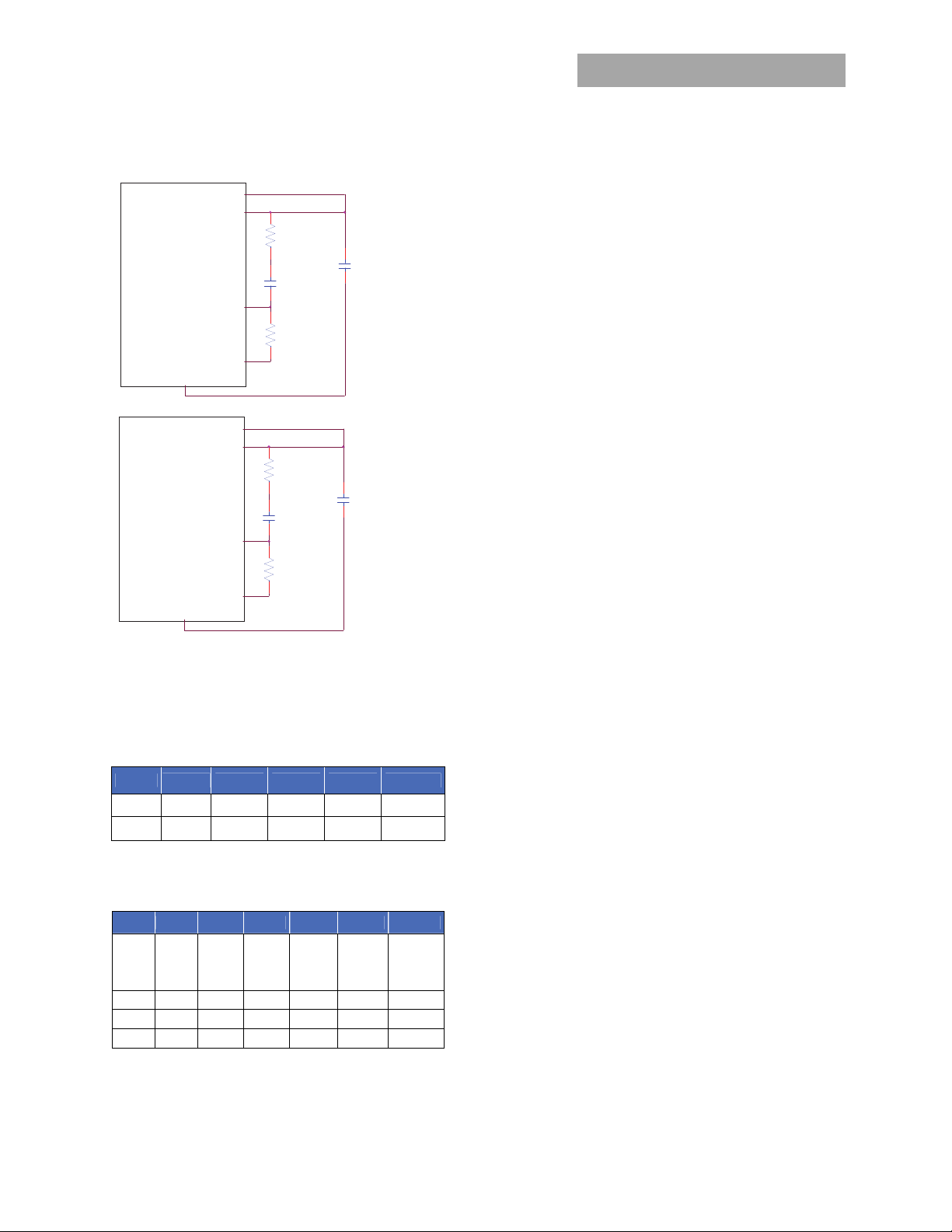
Tunable Loop
The module has a feature that optimizes transient response
of the module called Tunable Loop
External capacitors are usually added to the output of the
module for two reasons: to reduce output ripple and noise
(see Figure 38) and to reduce output voltage deviations from
the steady-state value in the presence of dynamic load
current changes. Adding external capacitance however
affects the voltage control loop of the module, typically
causing the loop to slow down with sluggish response.
Larger values of external capacitance could also cause the
module to become unstable.
The Tunable Loop
voltage control loop to match the filter network connected
to the output of the module. The Tunable Loop
implemented by connecting a series R-C between the VS+
and TRIM pins of the module, as shown in Fig. 47. This R-C
allows the user to externally adjust the voltage loop
feedback compensation of the module.
TM
TM
.
TM
allows the user to externally adjust the
TM
is
February 14, 2014 ©2014 General Electric Corporation. All rights reserved. Page 16
Page 17
GE
Datasheet
2 × 12A Digital Dual MicroDlynxTM: Non-Isolated DC-DC Power Modules
4.5Vdc –14.4Vdc input; 0.51Vdc to 5.5Vdc output; 2 × 12A Output Current
VOUT1
VS+1
MODULE
TRIM1
SIG_GND
GND
RTune
CTune
RTrim
CO
VOUT2
VS+2
RTune
MODULE
TRIM2
CTune
CO
RTrim
SIG_GND
GND
Figure. 47. Circuit diagram showing connection of R
and C
to tune the control loop of the module.
TUNE
TUME
Table 2. General recommended values of of R
for Vin=12V and various external ceramic capacitor
C
TUNE
TUNE
and
combinations.
Co
3x47μF 4x47μF 6x47μF 10x47μF 20x47μF
R
TUNE
300 300 300 300 300
C
TUNE
220pF 330pF 1000pF 1800pF 3900pF
Table 3. Recommended values of R
TUNE
and C
TUNE
to obtain
transient deviation of 2% of Vout for a 6A step load with
Vin=12V.
Vo 5V 3.3V 2.5V 1.8V 1.2V 0.6V
3x47μF
3x47μF
+
2x330μF
Polymer
3x47μF +
2x330μF
Polymer
Co
6x47μF
R
TUNE
300 300 300 300 300 300
C
TUNE
470pF 1200pF 1500pF 1800pF 2700pF 12nF
ΔV
84mV 39mV 30mV 27mV 20mV 10mV
+
330μF
Polymer
3x47μF +
3x330μF
Polymer
2x47μF +
7x330μF
Polymer
Note: The capacitors used in the Tunable Loop tables are
47 F/2 m ESR ceramic and 330 F/12 m ESR polymer
capacitors.
Recommended values of R
TUNE
and C
for different output
TUNE
capacitor combinations are given in Table 2. Table 2 shows
the recommended values of R
TUNE
and C
for different
TUNE
values of ceramic output capacitors up to 1000uF that
might be needed for an application to meet output ripple
and noise requirements. Selecting R
TUNE
and C
according
TUNE
to Table 2 will ensure stable operation of the module.
In applications with tight output voltage limits in the
presence of dynamic current loading, additional output
capacitance will be required. Table 3 lists recommended
values of R
TUNE
and C
in order to meet 2% output
TUNE
voltage deviation limits for some common output voltages
in the presence of a 6A to 12A step change (50% of full load),
with an input voltage of 12V.
Please contact your GE technical representative to obtain
more details of this feature as well as for guidelines on how
to select the right value of external R-C to tune the module
for best transient performance and stable operation for
other output capacitance values.
February 14, 2014 ©2014 General Electric Corporation. All rights reserved. Page 17
Page 18
A
A
GE
Datasheet
2 × 12A Digital Dual MicroDlynxTM: Non-Isolated DC-DC Power Modules
4.5Vdc –14.4Vdc input; 0.51Vdc to 5.5Vdc output; 2 × 12AOutput Current
Digital Feature Descriptions
PMBus Interface Capability
The 2 × 12A Digital Dual MicroDlynxTM power modules have
a PMBus interface that supports both communication and
control. The PMBus Power Management Protocol
Specification can be obtained from www.pmbus.org. The
modules support a subset of version 1.1 of the specification
(see Table 6 for a list of the specific commands supported).
Most module parameters can be programmed using PMBus
and stored as defaults for later use.
All communication over the module PMBus interface must
support the Packet Error Checking (PEC) scheme. The PMBus
master must generate the correct PEC byte for all
transactions, and check the PEC byte returned by the
module.
The module also supports the SMBALERT# response
protocol whereby the module can alert the bus master if it
wants to talk. For more information on the SMBus alert
response protocol, see the System Management Bus
(SMBus) specification.
The module has non-volatile memory that is used to store
configuration settings. Not all settings programmed into the
device are automatically saved into this non-volatile
memory, only those specifically identified as capable of
being stored can be saved (see Table 6 for which command
parameters can be saved to non-volatile storage).
PMBus Data Format
For commands that set thresholds, voltages or report such
quantities, the module supports the “Linear” data format
among the three data formats supported by PMBus. The
Linear Data Format is a two byte value with an 11-bit, two’s
complement mantissa and a 5-bit, two’s complement
exponent. The format of the two data bytes is shown below:
Data Byte High
7 6 5 4 3 2 1 0 7 6 5 4 3 2 1 0
Exponent
MSB
The value is of the number is then given by
PMBus Addressing
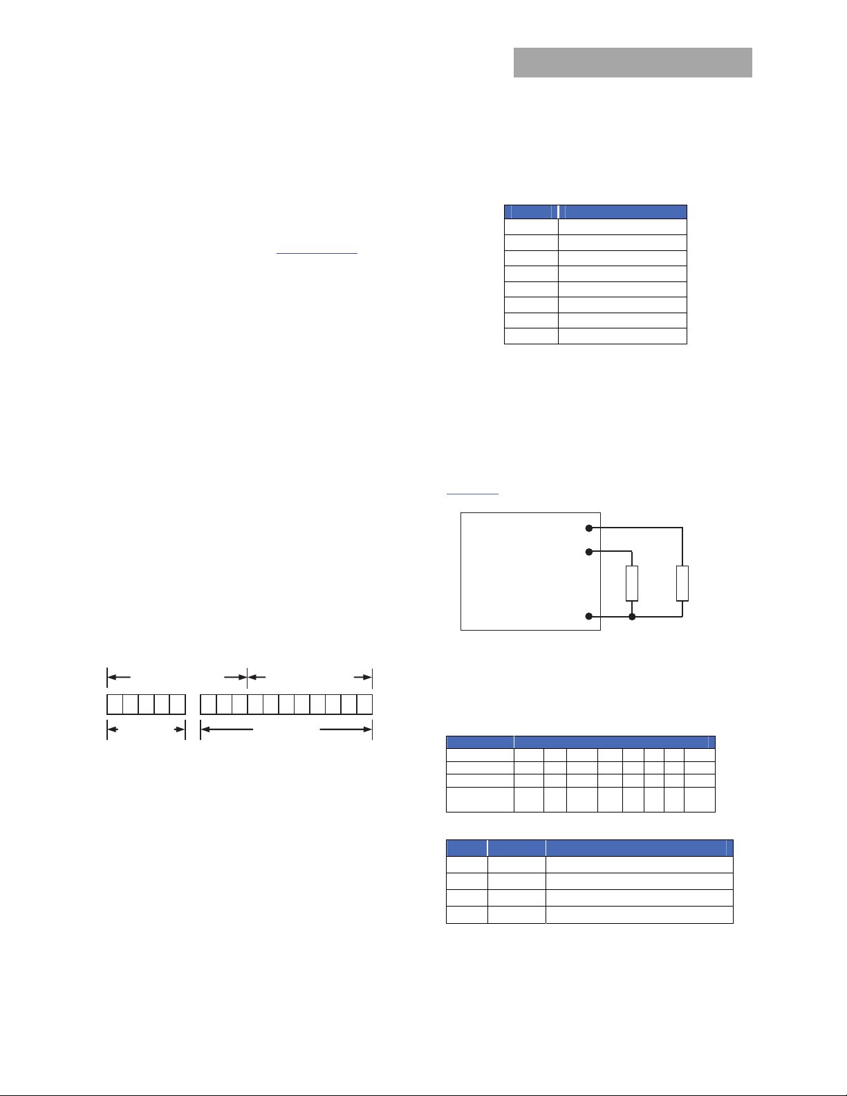
The power module can be addressed through the PMBus
using a device address. The module has 64 possible
addresses (0 to 63 in decimal) which can be set using
resistors connected from the ADDR0 and ADDR1 pins to
SIG_GND. Note that some of these addresses (0, 1, 2, 3, 4, 5,
6, 7, 8, 9, 10, 11 12, 40, 44, 45, 55 in decimal) are reserved
according to the SMBus specifications and may not be
useable. The address is set in the form of two octal (0 to 7)
digits, with each pin setting one digit. The ADDR1 pin sets
the high order digit and ADDR0 sets the low order digit. The
resistor values suggested for each digit are shown in Table 4
(1% tolerance resistors are recommended). Note that if
MSB
Value = Mantissa x 2
Data Byte Low
Mantissa
Exponent
either address resistor value is outside the range specified in
Table 4, the module will respond to address 127.
Table 4
Digit Resistor Value (K)
0 11
1 18.7
2 27.4
3 38.3
4 53.6
5 82.5
6 127
7 187
The user must know which I
2
C addresses are reserved in a
system for special functions and set the address of the
module to avoid interfering with other system operations.
Both 100kHz and 400kHz bus speeds are supported by the
module. Connection for the PMBus interface should follow
the High Power DC specifications given in section 3.1.3 in the
SMBus specification V2.0 for the 400kHz bus speed or the
Low Power DC specifications in section 3.1.2. The complete
SMBus specification is available from the SMBus web site,
smbus.org.
DDR1
DDR0
SIG_GND
R
ADDR0
R
ADDR1
Figure 48. Circuit showing connection of resistors used to
set the PMBus address of the module.
PAGE
Both the outputs of the module can be configured,
controlled and monitored through only one physical address
Format
Bit Position
Access
Function
Default
Value
7 6 5 4 3 2 1 0
r/w r r r
PA X X X X X X P0
0 X X X X X X 0
Unsigned Binary
r r r r/w
PAGE Command Truth Table
PA P0 Logic Results
0 0
0 1
1 0
1 1
If PAGE=11, then any read commands affect the first
channel. Any value to ready-only registers is ignored.
All Commands address first output
All Commands address second output
Illegal input, Ignore write
All Commands address both outputs
February 14, 2014 ©2014 General Electric Corporation. All rights reserved. Page 18
Page 19
GE
Datasheet
2 × 12A Digital Dual MicroDlynxTM: Non-Isolated DC-DC Power Modules
4.5Vdc –14.4Vdc input; 0.51Vdc to 5.5Vdc output; 2 × 12A Output Current
Operation (01h)
This is a paged register. The OPERATION command can be
use to turn the module on or off in conjunction with the
ON/OFF pin input. It is also used to margin up or margin
down the output voltage
PMBus Enabled On/Off
The module can also be turned on and off via the PMBus
interface. The OPERATION command is used to actually turn
the module on and off via the PMBus, while the
ON_OFF_CONFIG command configures the combination of
analog ON/OFF pin input and PMBus commands needed to
turn the module on and off. Bit [7] in the OPERATION
command data byte enables the module, with the following
functions:
0 : Output is disabled
1 : Output is enabled
This module uses the lower five bits of the ON_OFF_CONFIG
data byte to set various ON/OFF options as follows:
Bit Position 4 3 2 1 0
Access r/w r/w r/w r r
Function PU CMD CPR POL CPA
Default Value 1 0 1 1 0
PU: Sets the default to either operate any time input power
is present or for the ON/OFF to be controlled by the analog
ON/OFF input and the PMBus OPERATION command. This bit
is used together with the CP, CMD and ON bits to determine
startup.
Bit Value Action
Module powers up any time power is
0
present regardless of state of the analog
ON/OFF pin
Module does not power up until
commanded by the analog ON/OFF pin and
1
the OPERATION command as programmed
in bits [2:0] of the ON_OFF_CONFIG register.
CMD: The CMD bit controls how the device responds to the
OPERATION command.
Bit Value Action
Module ignores the ON bit in the
0
OPERATION command
Module responds to the ON bit in the
1
OPERATION command
CPR: Sets the response of the analog ON/OFF pin. This bit is
used together with the CMD, PU and ON bits to determine
startup.
Bit Value Action
Module ignores the analog ON/OFF pin, i.e.
0
ON/OFF is only controlled through the
PMBUS via the OPERATION command
Module requires the analog ON/OFF pin to
1
be asserted to start the unit
CPA: Sets the action of the analog ON/OFF pin when turning
the controller OFF. This bit is internally read and cannot be
modified by the user
PMBus Adjustable Soft Start Rise Time
The soft start rise time can be adjusted in the module via
PMBus. When setting this parameter, make sure that the
charging current for output capacitors can be delivered by
the module in addition to any load current to avoid nuisance
tripping of the overcurrent protection circuitry during
startup. The TON_RISE command sets the rise time in ms,
and allows choosing soft start times between 600s and
9ms, with possible values listed in Table 5. Note that the
exponent is fixed at -4 (decimal) and the upper two bits of
the mantissa are also fixed at 0.
February 14, 2014 ©2014 General Electric Corporation. All rights reserved. Page 19
Page 20

GE
Datasheet
2 × 12A Digital Dual MicroDlynxTM: Non-Isolated DC-DC Power Modules
4.5Vdc –14.4Vdc input; 0.51Vdc to 5.5Vdc output; 2 × 12AOutput Current
Table 5
Rise Time Exponent Mantissa
600s 11100 00000001010
900s 11100 00000001110
1.2ms 11100 00000010011
1.8ms 11100 00000011101
2.7ms 11100 00000101011
4.2ms 11100 00001000011
6.0ms 11100 00001100000
9.0ms 11100 00010010000
Output Voltage Adjustment Using the PMBus
The VREF_TRIM parameter is important for a number of
PMBus commands related to output voltage trimming, and
margining. Each of the 2 output voltages of the module shall
be set as the combination of the voltage divider formed by
RTrim and a 20k upper divider resistor inside the module,
and the internal reference voltage of the module. The
reference voltage V
the output regulation voltage is then given by
V ×
V ×
Hence the module output voltages shall be dependent on
the value of RTrim1 and Rtrim2 which are connected
external to the module.
The VREF_TRIM parameter is used to apply a fixed offset
voltage to the reference voltage shall be specified using the
“Linear” format and two bytes. The exponent is fixed at –9
(decimal). The resolution of the adjustment is 7 bits, with a
resulting step size of approximately 0.4%. The maximum
trim range is -20% to +10% of the nominal reference
voltage(600mV) in 2mV steps. Permissible values range from
-120mV to +60mV
When PMBus commands are used to trim or margin the
output voltage, the value of V
the module, which in turn changes the regulated output
voltage of the module.
The nominal output voltage of the module shall be
adjustable with a minimum step size of 0.4% over a +10% to
-20% range from nominal using the VREF_TRIM command
over the PMBus.
The VREF_TRIM command shall be used to apply a fixed
offset voltage to either of the output voltage command
value using the “Linear” mode with the exponent fixed at –9
(decimal). The value of the offset voltage shall be given by
shall be nominally set at 600mV, and
REF
)(
+
RTrim
+
RTrim
is what is changed inside
REF
=
1.
=
2.
offsetREF
RTrim
1
RTrim
2
120000
220000
V
REFOUT
×= TRIMVREFV
V
REFOUT
9
−
2_
This offset voltage shall be added to the voltage set through
the divider ratio and nominal V
output voltage. If a value outside of the +10%/-20%
adjustment range is given with this command, the module
shall set it’s output voltage to the upper or lower limit value
(as if VOUT_TRIM, assert SMBALRT#, set the CML bit in
STATUS_BYTE and the invalid data bit in STATUS_CML.
to produce the trimmed
REF
Output Voltage Margining Using the PMBus
Each output of the module shall also have its output voltage
margined via PMBus commands. The command
STEP_VREF_MARGIN_HIGH shall set the margin high voltage,
while the command STEP_VREF_MARGIN_LOW sets the
margin low voltage. Both the STEP_VREF_MARGIN_HIGH
and STEP_VREF_MARGIN_LOW commands shall use the
“Linear” mode with the exponent fixed at –9 (decimal). Two
bytes shall be used for the mantissa with the upper bit [7] of
the high byte shall be fixed at 0. The actual margined output
voltage shall be a combination of the
STEP_VREF_MARGIN_HIGH or STEP_VREF_MARGIN_LOW
and the VREF_TRIM values as shown below.
V
=
MHREF
)(
TRIMVREFHIGHMARGINVREFSTEP
V
=
MLREF
)(
TRIMVREFLOWMARGINVREFSTEP
The net permissible voltage range change shall be -30% to
+10% for the margin high command and -20% to 0% for the
margin low command
The module shall support the margined high or low voltages
using the OPERATION command. Bits [5:2] shall be used to
enable margining as follows:
00XX : Margin Off
0101 : Margin Low (Act on Fault)
0110 : Margin Low (Act on Fault)
1001 : Margin High (Act on Fault)
1010 : Margin High (Act on Fault)
PMBus Adjustable Overcurrent Warning
The module can provide an overcurrent warning via the
PMBus. The threshold for the overcurrent warning can be
set using the parameter IOUT_OC_WARN_LIMIT. This
command uses the “Linear” data format with a two byte
data word where the upper five bits [7:3] of the high byte
represent the exponent and the remaining three bits of the
high byte [2:0] and the eight bits in the low byte represent
the mantissa. The exponent is fixed at –1 (decimal). The
upper five bits of the mantissa are fixed at 0 while the lower
six bits are programmable with a default value of 19A
(decimal). The resolution of this warning limit is 500mA. The
value of the IOUT_OC_WARN_LIMIT can be stored to nonvolatile memory using the STORE_DEFAULT_ALL command.
Temperature Status via PMBus
The module will provide information related to temperature
of the module through the READ_TEMPERATURE_2
command. The command returns external temperature in
degrees Celsius. This command shall use the “Linear” data
9
−
2)____(
×+
9
−
2)____(
×+
February 14, 2014 ©2014 General Electric Corporation. All rights reserved. Page 20
Page 21

GE
Datasheet
2 × 12A Digital Dual MicroDlynxTM: Non-Isolated DC-DC Power Modules
4.5Vdc –14.4Vdc input; 0.51Vdc to 5.5Vdc output; 2 × 12A Output Current
format with a two byte data word where the upper five bits
[7:3] of the high byte shall represent the exponent and the
remaining three bits of the high byte [2:0] and the eight bits
in the low byte shall represent the mantissa. The exponent
is fixed at 0 (decimal). The lower 11 bits are the result of the
ADC conversion of the external temperature
PMBus Adjustable Output Over, Under Voltage
Protection and Power Good
The module has a common command to set the PGOOD,
VOUT_UNDER_VOLTAGE(UV) and VOUT_OVER_VOLTAGE (OV)
limits as a percentage of nominal. Refer to Table 6 of the
next section for the available settings. The PMBus command
VOUT_OVER_VOLTAGE (OV) shall be used to set the output
over voltage threshold from two possible values: +12.5% or
+16.67% of the commanded output voltage for each output.
The module provides a Power Good (PGOOD) for each output
signal that shall be implemented with an open-drain output
to indicate that the output voltage is within the regulation
limits of the power module. The PGOOD signal shall be deasserted to a low state if any condition such as
overtemperature, overcurrent or loss of regulation occurs
that would result in the output voltage going outside the
specified thresholds. The PGOOD thresholds shall be user
selectable via the PMBus (the default values are as shown in
the Feature Specifications Section). Each threshold shall be
set up symmetrically above and below the nominal value.
The PGL (POWERGOODLOW) command shall set the output
voltage level above which PGOOD is asserted (lower
threshold). The PGH(POWERGOODHIGH) command shall set
the level above which the PGOOD command is de-asserted.
This command shall also set two thresholds symmetrically
placed around the nominal output voltage. Normally, the
PGL threshold shall be set higher than the PGH threshold.
The PGOOD terminal can be connected through a pullup
resistor (suggested value 100KΩ) to a source of 5VDC or
lower. The current through the PGood terminal should be
limited to a max value of 5mA
PMBus Adjustable Input Undervoltage Lockout
The module allows for adjustment of the input under voltage
lockout and hysteresis. The command VIN_ON allows setting
the input voltage turn on threshold for each output, while
the VIN_OFF command shall set the input voltage turn off
threshold. For the VIN_ON command, possible values are
4.25V to 16V in variable steps. For the VIN_OFF command,
possible values are 4V to 15.75V in 0.5V steps. If other values
are entered for either command, they shall be mapped to
the closest of the allowed values.
Both the VIN_ON and VIN_OFF commands use the “Linear”
format with two data bytes. The upper five bits shall
represent the exponent (fixed at -2) and the remaining 11
bits shall represent the mantissa. For the mantissa, the four
most significant bits are fixed at 0.
Measurement of Output Current, Output Voltage
and Input Voltage
The module is capable of measuring key module
parameters such as output current and voltage for each
outputs and input voltage for each input and providing this
information through the PMBus interface.
Measuring Output Current Using the PMBus
The module measures current by using the inductor winding
resistance as a current sense element. The inductor winding
resistance is then the current gain factor used to scale the
measured voltage into a current reading. This gain factor is
the argument of the IOUT_CAL_GAIN command, and
consists of two bytes in the linear data format. The exponent
uses the upper five bits [7:3] of the high data byte in two-s
complement format and is fixed at –15 (decimal). The
remaining 11 bits in two’s complement binary format
represent the mantissa. During manufacture, each module
is calibrated by measuring and storing the current gain
factor into non-volatile storage.
The current measurement accuracy is also improved by
each module being calibrated during manufacture with the
offset in the current reading. The IOUT_CAL_OFFSET
command is used to store and read the current offset. The
argument for this command consists of two bytes
composed of a 5-bit exponent (fixed at -4d) and a 11-bit
mantissa. This command has a resolution of 62.5mA and a
range of -4000mA to +3937.5mA.
The READ_IOUT command provides module average output
current information. This command only supports positive or
current sourced from the module. If the converter is sinking
current a reading of 0 is provided. The READ_IOUT
command returns two bytes of data in the linear data
format. The exponent uses the upper five bits [7:3] of the
high data byte in two-s complement format and is fixed at –
4 (decimal). The remaining 11 bits in two’s complement
binary format represent the mantissa with the 11
at 0 since only positive numbers are considered valid.
th
bit fixed
Measuring Output Voltage Using the PMBus
The module provides output voltage information using the
READ_VOUT command for each output. In this module the
output voltage is sensed at the remote sense amplifier
output pin so voltage drop to the load is not accounted for.
The command shall return two bytes of data all representing
the mantissa while the exponent is fixed at -9 (decimal).
Reading the Status of the Module using the PMBus
The module supports a number of status information
commands implemented in PMBus. However, not all
features are supported in these commands. A 1 in the bit
position indicates the fault that is flagged.
STATUS_BYTE : Returns one byte of information with a
summary of the most critical device faults.
Bit
Position
7 X 0
6 OFF 0
5 VOUT Overvoltage 0
4 IOUT Overcurrent 0
Flag
Default
Value
February 14, 2014 ©2014 General Electric Corporation. All rights reserved. Page 21
Page 22
GE
Datasheet
2 × 12A Digital Dual MicroDlynxTM: Non-Isolated DC-DC Power Modules
4.5Vdc –14.4Vdc input; 0.51Vdc to 5.5Vdc output; 2 × 12AOutput Current
3 VIN Undervoltage 0
2 Temperature 0
1 CML (Comm. Memory Fault) 0
0 None of the above 0
STATUS_WORD : Returns two bytes of information with a
summary of the module’s fault/warning conditions.
Bit
Position
7 X 0
6 OFF 0
5 VOUT Overvoltage 0
4 IOUT Overcurrent 0
3 VIN Undervoltage 0
2 Temperature 0
1 CML (Comm. Memory Fault) 0
0 None of the above 0
Low Byte
Flag
Default
Value
High Byte
Bit
Position
7 VOUT fault or warning 0
6 IOUT fault or warning 0
5 X 0
4 MFR 0
3 POWER_GOOD# (is negated) 0
2 X 0
1 X 0
0 X 0
STATUS_VOUT : Returns one byte of information relating to
the status of the module’s output voltage related faults.
Bit
Position
7 VOUT OV Fault 0
6 X 0
5 X 0
4 VOUT UV Fault 0
3 X 0
2 X 0
1 X 0
0 X 0
STATUS_IOUT : Returns one byte of information relating to
the status of the module’s output voltage related faults.
Bit
Position
7 IOUT OC Fault 0
6 X 0
5 IOUT OC Warning 0
4 X 0
3 X 0
2 X 0
1 X 0
0 X 0
Flag
Flag
Flag
Default
Value
Default
Value
Default
Value
STATUS_TEMPERATURE : Returns one byte of information
relating to the status of the module’s temperature related
faults.
Bit
Position
7 OT Fault 0
6 OT Warning 0
5 X 0
4 X 0
3 X 0
2 X 0
1X 0
0 X 0
Flag
Default
Value
STATUS_CML : Returns one byte of information relating to
the status of the module’s communication related faults.
Bit
Position
7 Invalid/Unsupported Command 0
6 Invalid/Unsupported Command 0
5 Packet Error Check Failed 0
4 Memory Fault Detected 0
3 X 0
2 X 0
1 Other Communication Fault 0
0 X 0
Flag
Default
Value
MFR_VIN_MIN : Returns minimum input voltage as two data
bytes of information in Linear format (upper five bits are
exponent – fixed at -2, and lower 11 bits are mantissa in
two’s complement format – fixed at 12)
MFR_VOUT_MIN : Returns minimum output voltage as two
data bytes of information in Linear format (upper five bits
are exponent – fixed at -10, and lower 11 bits are mantissa
in two’s complement format – fixed at 614)
MFR_SPECIFIC_00 : Returns information related to the type
of module and revision number. Bits [7:2] in the Low Byte
indicate the module type (xxxxxx corresponds to the
UDXS1212 series of module), while bits [7:3] indicate the
revision number of the module.
Bit
Position
7:2 Module Name 000011
1:0 Reserved 10
Low Byte
Flag
Default
Value
High Byte
Bit
Position
7:3 Module Revision Number None
2:0 Reserved 000
Flag
Default
Value
February 14, 2014 ©2014 General Electric Corporation. All rights reserved. Page 22
Page 23
GE
Datasheet
2 × 12A Digital Dual MicroDlynxTM: Non-Isolated DC-DC Power Modules
4.5Vdc –14.4Vdc input; 0.51Vdc to 5.5Vdc output; 2 × 12A Output Current
Summary of Supported PMBus Commands
Please refer to the PMBus 1.1 specification for more details of these commands.
Table 6
Hex
Code
00 PAGE
01 OPERATION
02 ON_OFF_CONFIG
03 CLEAR_FAULTS
10 WRITE_PROTECT
Command Brief Description
Ability to configure, control and monitor each output by using only one physical
address of the module
Format
Bit Position
Access
Function
Default Value
PAGE Command Truth Table
PA P0 Logic Results
0 0
0 1
1 0
1 1
Turn Module on or off. Also used to margin the output voltage
Format
Bit Position
Access
Function
Default Value
Bit 7: 0 Output switching disabled
1 Output switching enabled
Margin: 00XX Margin Off
0101 Margin Low ( Act on fault)
0110 Margin Low (Act on fault)
1001 Margin High (Act on fault)
1010 Margin High (Act on fault)
Configures the ON/OFF functionality as a combination of analog ON/OFF pin
and PMBus commands
Format
Bit Position
Access
Function
Default Value
Refer to Page 19 for details on pu, cmd, cpr, pol and cpa
Clear any fault bits that may have been set, also releases the SMBALERT# signal
if the device has been asserting it.
Used to control writing to the module via PMBus. Copies the current register
setting in the module whose command code matches the value in the data byte
into non-volatile memory (EEPROM) on the module
Format
Bit Position
Access
Function
Default Value
Bit5: 0 – Enables all writes as permitted in bit6 or bit7
1 – Disables all writes except the WRITE_PROTECT, PAGE OPERATION
and ON_OFF_CONFIG (bit 6 and bit7 must be 0)
Bit 6: 0 – Enables all writes as permitted in bit5 or bit7
1 – Disables all writes except for the WRITE_PROTECT, PAGE and
OPERATION commands (bit5 and bit7 must be 0)
Bit7: 0 – Enables all writes as permitted in bit5 or bit6
1 – Disables all writes except for the WRITE_PROTECT command
(bit5 and bit6 must be 0)
7 6 5 4 3 2 1 0
r/w r r r r r r r/w
PA X X X X X X P0
0 X X X X X X 0
All Commands address first output
All Commands address second output
All Commands address both outputs
7 6 5 4 3 2 1 0
r/w r r/w r/w r/w r/w r r
On X Margin X X
0 0 0 0 0 0 X X
7 6 5 4 3 2 1 0
r r r r/w r/w r/w r/w r
X X X pu cmd cpr pol cpa
0 0 0 1 0 1 1 0
7 6 5 4 3 2 1 0
r/w r/w r/w x x x x x
bit7 bit6 bit5 X X X X X
0 0 0 X X X X X
Unsigned Binary
Illegal input, Ignore write
Unsigned Binary
Unsigned Binary
Unsigned Binary
Non-Volatile
Memory Storage
YES
YES
15 STORE_USER_ALL
February 14, 2014 ©2014 General Electric Corporation. All rights reserved. Page 23
Stores all of the current storable register settings in the EEPROM memory as the
new defaults on power up
Page 24
GE
Datasheet
2 × 12A Digital Dual MicroDlynxTM: Non-Isolated DC-DC Power Modules
4.5Vdc –14.4Vdc input; 0.51Vdc to 5.5Vdc output; 2 × 12AOutput Current
Hex
Code
16 RESTORE_USER_ALL
19 CAPABILITY
20 VOUT_MODE
35 VIN_ON
36 VIN_OFF
Command Brief Description
Restores all of the storable register settings from the non-volatile memory
(EEPROM). The command should not be used while the device is actively
switching
This command helps the host system/GUI/CLI determine key capabilities of the
module
Format
Bit Position
Access
Function
Default Value
PEC – 1 Supported
SPD -01 – max of 400kHZ
ALRT – 1 – SMBALERT# supported
The module has MODE set to Linear and Exponent set to -10. These values
cannot be changed
Bit Position
Access
Function
Default Value
Mode: Value fixed at 000, linear mode
Exponent: Value fixed at 10111, Exponent for linear mode values is -9
Sets the value of input voltage at which the module turns on
Format
Bit Position
Access
Function
Default Value
Bit Position
Access
Function
Default Value
Exponent -2 (dec), fixed
Mantissa
The upper four bits are fixed at 0
The lower seven are programmable with a default value of 9(dec). This
corresponds to a default of 4.25V. Allowable values are
• 4.25, in steps of 0.25V upto 9.5V.
• 9.5V to 13V in increments of 0.5V
• 13V to 16V in increments of 1V
Sets the value of input voltage at which the module turns off
Format
Bit Position
Access
Function
Default Value
Bit Position
Access
Function
Default Value
Exponent -2 (dec), fixed
Mantissa
The upper four bits are fixed at 0
The lower seven are programmable with a default value of 8(dec). This
corresponds to a default of 4.0V.
Allowable values are
• 4.00, in steps of 0.25V upto 9.75V.
• 10.25V to 11.75V in increments of 0.5V
• 12V
• 13.75V to 16.75V in increments of 1V
7 6 5 4 3 2 1 0
r r r r r r r r
PEC SPD ALRT Reserved
1 0 1 1 0 0 0 0
7 6 5 4 3 2 1 0
r r r r r r r r
Mode Exponent
0 0 0 1 0 1 1 1
7 6 5 4 3 2 1 0
r r r r r r r r
1 1 1 1 0 0 0 0
7 6 5 4 3 2 1 0
r r/w r/w r/w r/w r/w r/w r/w
0 0 0 1 0 0 0 1
7 6 5 4 3 2 1 0
r r r r r r r r
1 1 1 1 0 0 0 0
7 6 5 4 3 2 1 0
r r/w r/w r/w r/w r/w r/w r/w
0 0 0 0 1 0 0 0
Unsigned Binary
Linear, two’s complement binary
Exponent Mantissa
Mantissa
Linear, two’s complement binary
Exponent Mantissa
Mantissa
Non-Volatile
Memory Storage
YES
YES
February 14, 2014 ©2014 General Electric Corporation. All rights reserved. Page 24
Page 25
GE
Datasheet
2 × 12A Digital Dual MicroDlynxTM: Non-Isolated DC-DC Power Modules
4.5Vdc –14.4Vdc input; 0.51Vdc to 5.5Vdc output; 2 × 12A Output Current
Hex
Code
Command Brief Description
38 IOUT_CAL_GAIN
39 IOUT_CAL_OFFSET
46
IOUT_OC_FAULT_LIMIT
Value maybe locked
47 IOUT_OC_FAULT_RESPONSE
4A
IOUT_OC_WARN_LIMIT
Value may be locked
Returns the value of the gain correction term used to correct the measured
output current
Format
Bit Position
Access
Function
Default Value
Bit Position
Access
Function
Default Value
7 6 5 4 3 2 1 0
r r r r r r r r/w
1 0 0 0 1 0 0 V
7 6 5 4 3 2 1 0
r/w r/w r/w r/w r/w r/w r/w r/w
Linear, two’s complement binary
Exponent Mantissa
Mantissa
V: Variable based on factory calibration
Returns the value of the offset correction used to correct the measured output
current
Format
Bit Position
Access
Function
Default Value
Bit Position
Access
Function
Default Value
7 6 5 4 3 2 1 0
r r r r r r/w r r
1 1 1 0 0 V V V
7 6 5 4 3 2 1 0
r r r/w r/w r/w r/w r/w r/w
Linear, two’s complement binary
Exponent Mantissa
Mantissa
V: Variable based on factory calibration
Sets the output overcurrent fault level in A (cannot be changed)
Format
Bit Position
Access
Function
Default Value
Bit Position
Access
Function
Default Value
7 6 5 4 3 2 1 0
r r r r r r r r
1 1 1 1 1 0 0 0
7 6 5 4 3 2 1 0
r r/w r/w r/w r/w r/w r/w r/w
0 0 1 0 1 0 0 0
Linear, two’s complement binary
Exponent Mantissa
Mantissa
Determines module action in response to an IOU_OC_FAULT_LIMIT or a VOUT
undervoltage (UV) fault
Format
Bit Position
Access
Function
Default Value
7 6 5 4 3 2 1 0
r r r/w r/w r/w r r r
X X
0 0 1 1 1 1 0 0
Unsigned Binary
RS
RS
[2]
[1]
RS
x X X
[0]
RS[2:0] – Retry Setting
000 Unit does not attempt to restart
111 Unit goes through normal soft start continuously
Any other value is not acceptable
Sets the output overcurrent warning level in A
Format
Bit Position
Access
Function
Default Value
Bit Position
Access
Function
Default Value
7 6 5 4 3 2 1 0
r r r r r r r r
1 1 1 1 1 0 0 0
7 6 5 4 3 2 1 0
r r/w r/w r/w r/w r/w r/w r/w
0 0 1 0 0 1 1 0
Linear, two’s complement binary
Exponent Mantissa
Mantissa
Non-Volatile
Memory Storage
YES
YES
YES
YES
February 14, 2014 ©2014 General Electric Corporation. All rights reserved. Page 25
Page 26

GE
Datasheet
2 × 12A Digital Dual MicroDlynxTM: Non-Isolated DC-DC Power Modules
4.5Vdc –14.4Vdc input; 0.51Vdc to 5.5Vdc output; 2 × 12AOutput Current
Hex
Code
Command Brief Description
4F
OT_FAULT_LIMIT
Value may be locked
51
OT_WARN_LIMIT
Value may be locked
61 TON_RISE
78 STATUS_BYTE
79 STATUS_WORD
7A STATUS_VOUT
Sets the overtemperature fault level in °C
Format
Bit Position
Access
Function
Default Value
Bit Position
Access
Function
Default Value
7 6 5 4 3 2 1 0
r r r r r r r r
0 0 0 0 0 0 0 0
7 6 5 4 3 2 1 0
r/w r/w r/w r/w r/w r/w r/w r/w
1 0 0 0 0 1 1 1
Linear, two’s complement binary
Exponent Mantissa
Mantissa
Sets the over temperature warning level in °C
Format
Bit Position
Access
Function
Default Value
Bit Position
Access
Function
Default Value
7 6 5 4 3 2 1 0
r r r r r r r r
0 0 0 0 0 0 0 0
7 6 5 4 3 2 1 0
r/w r/w r/w r/w r/w r/w r/w r/w
0 1 1 1 1 1 0 1
Linear, two’s complement binary
Exponent Mantissa
Mantissa
Sets the rise time of the output voltage during startup.
Supported Values – 0.6, 0.9, 1.2, 1.8, 2.7, 4.2, 6.0, 9.0msec. Value of 0 instructs unit to
bring its output to programmed value as quickly as possible
Format
Bit Position
Access
Function
Default Value
Bit Position
Access
Function
Default Value
7 6 5 4 3 2 1 0
r r r r r r r r/w
1 1 1 0 0 0 0 0
7 6 5 4 3 2 1 0
r/w r/w r/w r/w r/w r/w r/w r/w
0 0 1 0 1 0 1 1
Linear, two’s complement binary
Exponent Mantissa
Mantissa
Returns one byte of information with a summary of the most critical module faults
Format
Bit Position
Access
Flag
Default Value
7 6 5 4 3 2 1 0
r r r r r r r r
X OFF
0 0 0 0 0 0 0 0
Unsigned Binary
VOUT
IOUT_
_OV
OC
VIN_U
V
TEMP CML
None
of the
Above
Returns two bytes of information with a summary of the module’s fault/warning
conditions
Format
Bit Position
Access
Default Value
Bit Position
Access
Default Value
Flag
Flag
7 6 5 4 3 2 1 0
r r r r r r r r
IOUT/P
VOUT
OUT
0 0 0 0 0 0 0 0
7 6 5 4 3 2 1 0
r r r r r r r r
X OFF
0 X 0 0 0 0 0 0
Unsigned Binary
X MFR PGOOD X X X
VOUT_
OV
IOUT_
OC
VIN_U
V
TEMP CML
None
of the
above
Returns one byte of information with the status of the module’s output voltage related
faults
Format
Bit Position
Access
Flag
Default Value
7 6 5 4 3 2 1 0
r r r r r r r r
VOUT_OV X X VOUT_UV X X X X
0 0 0 0 0 0 0 0
Unsigned Binary
Non-Volatile
Memory Storage
YES
YES
YES
February 14, 2014 ©2014 General Electric Corporation. All rights reserved. Page 26
Page 27

GE
Datasheet
2 × 12A Digital Dual MicroDlynxTM: Non-Isolated DC-DC Power Modules
4.5Vdc –14.4Vdc input; 0.51Vdc to 5.5Vdc output; 2 × 12A Output Current
Hex
Code
7B STATUS_IOUT
7D STATUS_TEMPERATURE
7E STATUS_CML
80 STATUS_MFR_SPECIFIC
8B READ_VOUT
8C READ_IOUT
Command Brief Description
Returns one byte of information with the status of the module’s output current related
faults
Format
Bit Position
Access
Flag
Default Value
Returns one byte of information with the status of the module’s temperature related
faults
Format
Bit Position
Access
Flag
Default Value
Returns one byte of information with the status of the module’s communication related
faults
Format
Bit Position
Access
Flag
Default Value
Returns one byte of information with the status of the module specific faults or warning
Format
Bit Position
Access
Flag
Default Value
OTFI – Internal Temperature above Thermal Shutdown threshold
IVADDR – PMBUs address is not valid
TWOPH_EN – Module is in 2 phase mode
Returns the value of the output voltage of the module. Exponent is fixed at -9.
Format
Bit Position
Access
Function
Default Value
Bit Position
Access
Function
Default Value
Returns the value of the output current of the module
Format
Bit Position
Access
Function
Default Value
Bit Position
Access
Function
Default Value
V - Variable
7 6 5 4 3 2 1 0
r r r r r
IOUT_OC Fault X IOUT OC Warning X X X X X
0 0 0 0 0 0 0 0
7 6 5 4 3 2 1 0
r r r r r r r r
OT_FAULT OT_WARN X X X X X X
0 0 0 0 0 0 0 0
7 6 5 4 3 2 1 0
r r r r r r r r
Invalid
Command
7 6 5 4 3 2 1 0
r r r r r r r R
OTFI x X IVADDR X X X TWOPH_EN
0 0 0 0 0 0 0 0
Invalid
Data
0 0 0 0 0 0 0 0
Linear, two’s complement binary
7 6 5 4 3 2 1 0
r r r r r r r r
0 0 0 0 0 0 0 0
7 6 5 4 3 2 1 0
r r r r r r r r
0 0 0 0 0 0 0 0
Linear, two’s complement binary
7 6 5 4 3 2 1 0
r r r r R r r r
Exponent Mantissa
1 1 1 0 0 V V V
7 6 5 4 3 2 1 0
r r r r r r r r
V V V V V V V 0
Unsigned Binary
Unsigned Binary
Unsigned Binary
Memory
PEC
fault
Fail
detected
Unsigned Binary
Mantissa
Mantissa
Mantissa
X X
r r r
Other
Comm
Fault
X
Non-Volatile
Memory Storage
February 14, 2014 ©2014 General Electric Corporation. All rights reserved. Page 27
Page 28

GE
Datasheet
2 × 12A Digital Dual MicroDlynxTM: Non-Isolated DC-DC Power Modules
4.5Vdc –14.4Vdc input; 0.51Vdc to 5.5Vdc output; 2 × 12AOutput Current
Table 6 (Continued)
Hex
Code
8E READ_TEMPERATURE_2
98 PMBUS_REVISION
D0 MFR_SPECIFIC_00
D4 VREF_TRIM
D5 STEP_VREF_MARGIN_HIGH
Command Brief Description
Returns the value of the external temperature in degree Celsius
Format
Bit Position
Access
Function
Default Value
Bit Position
Access
Function
Default Value
V - Variable
Returns one byte indicating the module is compliant to PMBus Spec. 1.1 (read only)
Format
Bit Position
Access
Default Value
Returns module name information
Format
Bit Position
Access
Function
Default Value
Bit Position
Access
Function
Default Value
Applies a fixed offset to the reference voltage. Max trim range is -20% to +10% in 2mV
steps. Permissible values range between -120mV and +60mV. The offset is calculated
as VREF_TRIMx2
Format
Bit Position
Access
Function
Default Value
Bit Position
Access
Function
Default Value
Applies a fixed offset to the reference voltage. Adjustment is 0% to +10% in 2mV steps.
Permissible values range between 0mV and +60mV. The offset is calculated as
(STEP_VREF_MARGIN_HIGH + VREF_TRIM)x2
voltage includes VREF_TRIM adjustment and ranges from -30% to 10%
Format
Bit Position
Access
Function
Default Value
Bit Position
Access
Function
Default Value
7 6 5 4 3 2 1 0
r r r r R r r r
0 0 0 0 0 V V V
7 6 5 4 3 2 1 0
r r r r r r r r
V V V V V V V 0
7 6 5 4 3 2 1 0
r r r r r r r r
0 0 0 1 0 0 0 1
7 6 5 4 3 2 1 0
r r r r r r r r
1 1 1 0 1 0 0 0
7 6 5 4 3 2 1 0
r r r r r r r r
0 0 0 0 1 1 1 0
-9
. Exponent fixed at -9(dec)
7 6 5 4 3 2 1 0
r/w r r r r r r r
V V V V V V V V
7 6 5 4 3 2 1 0
r r r/w r/w r/w r/w r/w r/w
V V V V V V V V
7 6 5 4 3 2 1 0
r r r r r r r r
V V V V V V V V
7 6 5 4 3 2 1 0
r r r r/w r/w r/w r/w r/w
V V V V V V V V
Linear, two’s complement binary
Exponent Mantissa
Mantissa
Unsigned Binary
Unsigned Binary
Reserved
Module Name Reserved
Linear, two’s complement binary
Mantissa
Mantissa
-9
. Exponent fixed at -9(dec). Net output
Linear, two’s complement binary
Mantissa
Mantissa
Non-Volatile
Memory Storage
YES
YES
YES
February 14, 2014 ©2014 General Electric Corporation. All rights reserved. Page 28
Page 29

GE
Datasheet
2 × 12A Digital Dual MicroDlynxTM: Non-Isolated DC-DC Power Modules
4.5Vdc –14.4Vdc input; 0.51Vdc to 5.5Vdc output; 2 × 12A Output Current
Table 6 (Continued)
Hex
Code
D6 STEP_VREF_MARGIN_LOW
D7 PCT_VOUT_FAULT_PG_LIMIT
D8 SEQUENCE_TON_TOFF_DELAY
Command Brief Description
Applies a fixed negative offset to the reference voltage. Adjustment is -20% to 0% in
2mV steps. Permissible values range between -120mV and 0mV) The offset is
calculated as (STEP_VREF_MARGIN_HIGH + VREF_TRIM)x2
Net output voltage includes VREF_TRIM adjustment and ranges from -30% to 10%
Format
Bit Position
Access
Function
Default Value
Bit Position
Access
Function
Default Value
Single command to set PGOOD, VOUT_UNDER_VOLTAGE(UV) and
VOUT_OVER_VOLTAGE(OV) limits as percentage of nominal
Format
Bit Position
Access
Function
Default Value
PAGE Command Truth Table
PCT_M
Used to set delay to turn-on or turn-off modules as a ratio of TON_RISE. Values can
range from 1 to 7
Default Value
PCT_L
SB
0 0 -16.67 -12.5 -8.33 12.5 8.33 16.67
0 1 -12.5 -8.33 -4.17 8.33 4.17 12.5
1 0 -29.17 -20.83 -16.67 8.33 4.17 12.5
1 1 -41.67 -37.5 -33.33 8.33 4.17 12.5
Format
Bit Position
Access
7 6 5 4 3 2 1 0
r r r r r r r r
V V V V V V V V
7 6 5 4 3 2 1 0
r r r/w r/w r/w r/w r/w r/w
V V V V V V V V
UV (%) PGL
SB
7 6 5 4 3 2 1 0
r/w r/w r/w r r/w r/w r/w r
0 0 0 0 0 0 0 0
Linear, two’s complement binary
Mantissa
Mantissa
Unsigned Binary
7 6 5 4 3 2 1 0
r r r
X X X X X X
0 X X X X X X 0
r r r r/w r/w
LOW
(%)
PGL
HIGH
(%)
Unsigned Binary
-9
.Exponent fixed at -9(dec).
PCT_
MSB
PGH
HIGH
(%)
PGH
LOW
(%)
OV (%)
Non-Volatile
Memory
Storage
YES
PCT_
LSB
February 14, 2014 ©2014 General Electric Corporation. All rights reserved. Page 29
Page 30

Air
GE
Datasheet
2 × 12A Digital Dual MicroDlynxTM: Non-Isolated DC-DC Power Modules
4.5Vdc –14.4Vdc input; 0.51Vdc to 5.5Vdc output; 2 × 12AOutput Current
Thermal Considerations
Power modules operate in a variety of thermal
environments; however, sufficient cooling should always be
provided to help ensure reliable operation.
Considerations include ambient temperature, airflow,
module power dissipation, and the need for increased
reliability. A reduction in the operating temperature of the
module will result in an increase in reliability. The thermal
data presented here is based on physical measurements
taken in a wind tunnel. The test set-up is shown in Figure
49. The preferred airflow direction for the module is in
Figure 50.
25.4_
Wind Tunnel
PWBs
(1.0)
Power Module
The thermal reference points, T
are also shown in Figure 50. For reliable operation the
temperatures at these points should not exceed 135
output power of the module should not exceed the rated
power of the module (Vo,set x Io,max).
Please refer to the Application Note “Thermal
Characterization Process For Open-Frame Board-Mounted
Power Modules” for a detailed discussion of thermal
aspects including maximum device temperatures.
used in the specifications
ref
o
C. The
Figure 50. Preferred airflow direction and location of hotspot of the module (Tref).
x
12.7_
(0.50)
76.2_
(3.0)
Probe Location
for measuring
airflow and
ambient
temperature
flow
Figure 49. Thermal Test Setup.
February 14, 2014 ©2014 General Electric Corporation. All rights reserved. Page 30
Page 31

A
A
GE
Datasheet
2 × 12A Digital Dual MicroDlynxTM: Non-Isolated DC-DC Power Modules
4.5Vdc –14.4Vdc input; 0.51Vdc to 5.5Vdc output; 2 × 12A Output Current
Example Application Circuit
Requirements:
Vin: 12V
Vout: 1.8V
Iout: 2 × 9A max., worst case load transient is from 6A to 9A
ΔVout: 1.5% of Vout (27mV) for worst case load transient
Vin, ripple 1.5% of Vin (180mV, p-p)
CI3
Vin+
CI2
CI1
VIN1
PGOOD1
MODULE
SYNC
CLK
DATA
SMBALRT#
ON/OFF1
VOUT1
VS+1
TRIM1
DDR0
DDR1
SIG_GND
RADDR1
RTUNE1
CTUNE2
RTrim1
RADDR0
Vout+
CO1
CO2
CO3
PGND
TRIM2
VS+2
VOUT2
RTrim2
RTUNE2
CTUNE2
CO4
CO5
CO6
GND
PGND
ON/OFF2
PGOOD2
VIN2
CI1 Decoupling cap - 4x0.1μF/16V, 0402 size ceramic capacitor
CI2 4x22μF/16V ceramic capacitor (e.g. Murata GRM32ER61C226KE20)
CI3 470μF/16V bulk electrolytic
CO1 Decoupling cap - 2x0.1μF/16V, 0402 size ceramic capacitor
CO2 3 x 47μF/6.3V ceramic capacitor (e.g. Murata GRM31CR60J476ME19)
CO3 1 x 330μF/6.3V Polymer (e.g. Sanyo Poscap)
CO4 Decoupling cap - 2x0.1μF/16V, 0402 size ceramic capacitor
CO5 3 x 47μF/6.3V ceramic capacitor (e.g. Murata GRM31CR60J476ME19)
CO6 1 x 330μF/6.3V Polymer (e.g. Sanyo Poscap)
CTune1 1200pF ceramic capacitor (can be 1206, 0805 or 0603 size)
RTune1 300 ohms SMT resistor (can be 1206, 0805 or 0603 size)
RTrim1 10kΩ SMT resistor (can be 1206, 0805 or 0603 size, recommended tolerance of 0.1%)
CTune2 1200pF ceramic capacitor (can be 1206, 0805 or 0603 size)
RTune2 300 ohms SMT resistor (can be 1206, 0805 or 0603 size)
RTrim2 10kΩ SMT resistor (can be 1206, 0805 or 0603 size, recommended tolerance of 0.1%)
Note: The DATA, CLK and SMBALRT pins do not have any pull-up resistors inside the module. Typically, the SMBus master
controller will have the pull-up resistors as well as provide the driving source for these signals.
February 14, 2014 ©2014 General Electric Corporation. All rights reserved. Page 31
Page 32
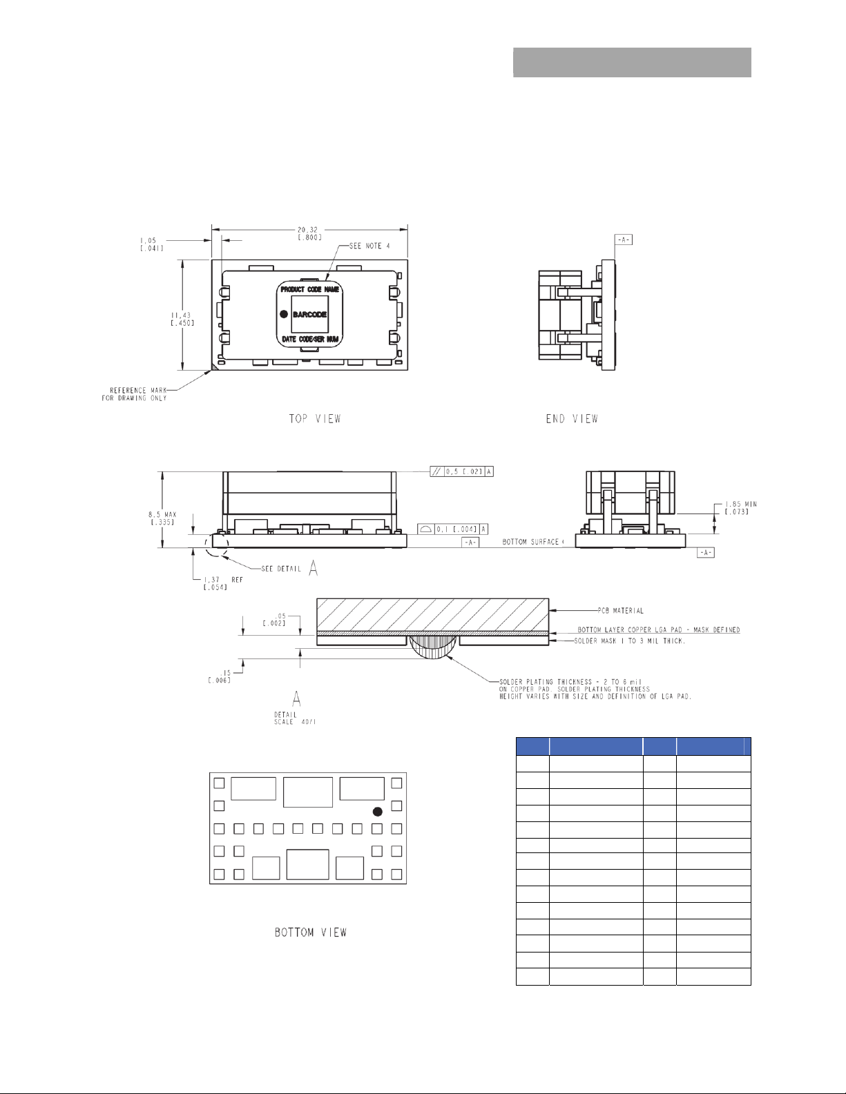
GE
Datasheet
2 × 12A Digital Dual MicroDlynxTM: Non-Isolated DC-DC Power Modules
4.5Vdc –14.4Vdc input; 0.51Vdc to 5.5Vdc output; 2 × 12AOutput Current
Mechanical Outline
Dimensions are in millimeters and (inches).
Tolerances: x.x mm
x.xx mm
±
0.5 mm (x.xx in. ± 0.02 in.) [unless otherwise indicated]
±
0.25 mm (x.xxx in ± 0.010 in.)
1
18
19
17
28
16
15 14
2
20
22 23 2425
21
12
13
11
5
43
6
26
7
27
8
10
9
PIN FUNCTION PIN FUNCTION
1 VSNS1 15 ADDR1
2 VOUT1 16 TRIM1
3 PGND 17 Sig_GND
4 VOUT2 18 TRIM2
5 VSNS2 19 SYNC
6 SMBALERT# 20 PGND
7 DATA 21 PGND
8 CLK 22 PGND
9 ENABLE1 23 PGND
10 ENABLE2 24 PGND
11 VIN 25 PGND
12 PGND 26 PGND
13 VIN 27 PGOOD2
14 ADDRO 28 PGOOD1
February 14, 2014 ©2014 General Electric Corporation. All rights reserved. Page 32
Page 33
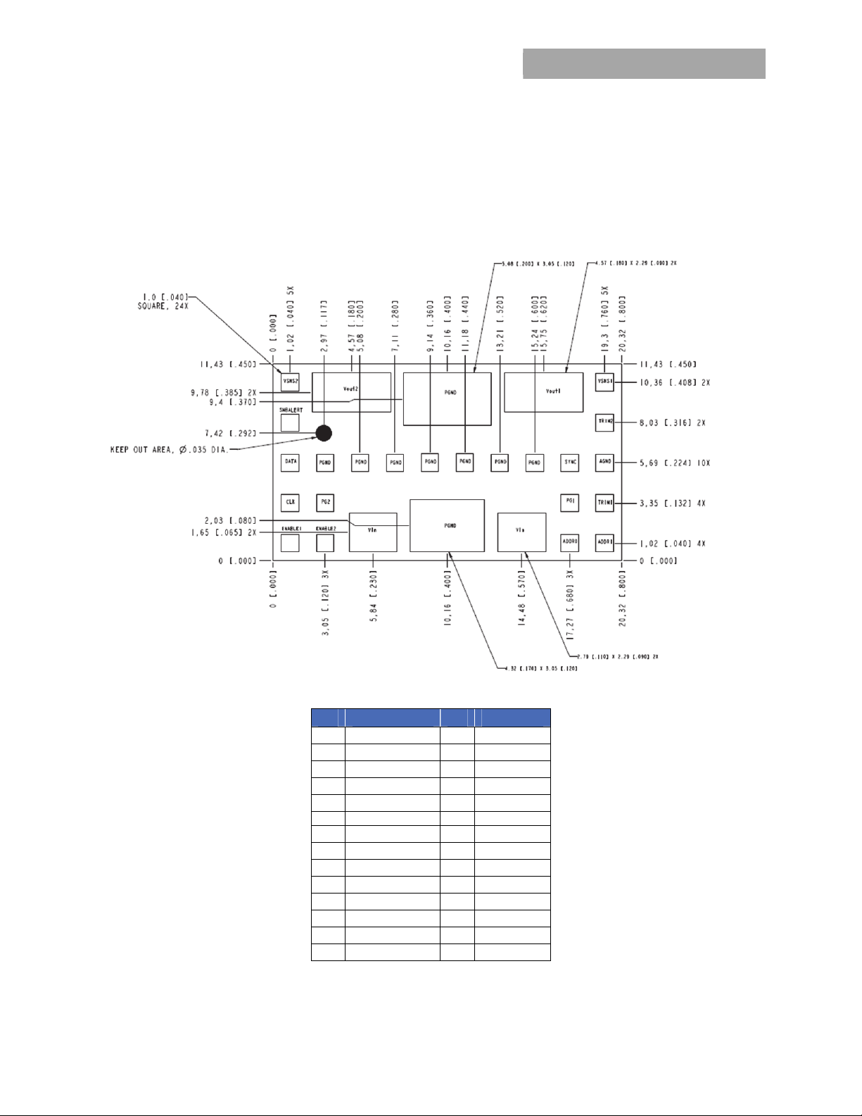
GE
Datasheet
2 × 12A Digital Dual MicroDlynxTM: Non-Isolated DC-DC Power Modules
4.5Vdc –14.4Vdc input; 0.51Vdc to 5.5Vdc output; 2 × 12A Output Current
Recommended Pad Layout
Dimensions are in millimeters and (inches).
Tolerances: x.x mm
x.xx mm
±
0.5 mm (x.xx in. ± 0.02 in.) [unless otherwise indicated]
±
0.25 mm (x.xxx in ± 0.010 in.)
February 14, 2014 ©2014 General Electric Corporation. All rights reserved. Page 33
PIN FUNCTION PIN FUNCTION
1 VSNS1 15 ADDR1
2 VOUT1 16 TRIM1
3 PGND 17 Sig_GND
4 VOUT2 18 TRIM2
5 VSNS2 19 SYNC
6 SMBALERT# 20 PGND
7 DATA 21 PGND
8 CLK 22 PGND
9 ENABLE1 23 PGND
10 ENABLE2 24 PGND
11 VIN 25 PGND
12 PGND 26 PGND
13 VIN 27 PGOOD2
14 ADDRO 28 PGOOD1
Page 34
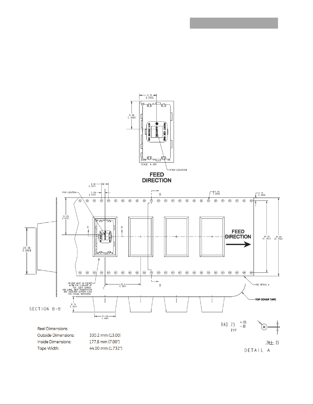
GE
Datasheet
2 × 12A Digital Dual MicroDlynxTM: Non-Isolated DC-DC Power Modules
4.5Vdc –14.4Vdc input; 0.51Vdc to 5.5Vdc output; 2 × 12AOutput Current
Packaging Details
The 12V Digital Dual MicroDlynxTM2 × 12A modules are supplied in tape & reel as standard. Modules are shipped in quantities of
200 modules per reel.
All Dimensions are in millimeters and (in inches).
Reel Dimensions:
Outside Dimensions: 330.2 mm (13.00)
Inside Dimensions: 177.8 mm (7.00”)
Tape Width: 44.00 mm (1.732”)
February 14, 2014 ©2014 General Electric Corporation. All rights reserved. Page 34
Page 35
GE
Datasheet
2 × 12A Digital Dual MicroDlynxTM: Non-Isolated DC-DC Power Modules
4.5Vdc –14.4Vdc input; 0.51Vdc to 5.5Vdc output; 2 × 12A Output Current
Surface Mount Information
Pick and Place
The2 × 12A Digital Dual MicroDlynxTM modules use an open
frame construction and are designed for a fully automated
assembly process. The modules are fitted with a label
designed to provide a large surface area for pick and place
operations. The label meets all the requirements for surface
mount processing, as well as safety standards, and is able
to withstand reflow temperatures of up to 300
also carries product information such as product code,
serial number and the location of manufacture.
Nozzle Recommendations
The module weight has been kept to a minimum by using
open frame construction. Variables such as nozzle size, tip
style, vacuum pressure and placement speed should be
considered to optimize this process. The minimum
recommended inside nozzle diameter for reliable operation
is 3mm. The maximum nozzle outer diameter, which will
safely fit within the allowable component spacing, is 7 mm.
Bottom Side / First Side Assembly
This module is not recommended for assembly on the
bottom side of a customer board. If such an assembly is
attempted, components may fall off the module during the
second reflow process.
Lead Free Soldering
The modules are lead-free (Pb-free) and RoHS compliant
and fully compatible in a Pb-free soldering process. Failure
to observe the instructions below may result in the failure of
or cause damage to the modules and can adversely affect
long-term reliability.
Pb-free Reflow Profile
Power Systems will comply with J-STD-020 Rev. D
(Moisture/Reflow Sensitivity Classification for Nonhermetic
Solid State Surface Mount Devices) for both Pb-free solder
profiles and MSL classification procedures. This standard
provides a recommended forced-air-convection reflow
profile based on the volume and thickness of the package
(table 4-2). The suggested Pb-free solder paste is Sn/Ag/Cu
(SAC). The recommended linear reflow profile using
Sn/Ag/Cu solder is shown in Fig. 50. Soldering outside of the
recommended profile requires testing to verify results and
performance.
MSL Rating
The2 x 12A Digital Dual MicroDlynxTM modules have a MSL
rating of 3
o
C. The label
packages should not be broken until time of use. Once the
original package is broken, the floor life of the product at
conditions of
according to the MSL rating (see J-STD-033A). The shelf life
for dry packed SMT packages will be a minimum of 12
months from the bag seal date, when stored at the following
conditions: < 40° C, < 90% relative humidity.
Figure 51. Recommended linear reflow profile using
Sn/Ag/Cu solder.
≤
30°C and 60% relative humidity varies
Post Solder Cleaning and Drying Considerations
Post solder cleaning is usually the final circuit-board
assembly process prior to electrical board testing. The result
of inadequate cleaning and drying can affect both the
reliability of a power module and the testability of the
finished circuit-board assembly. For guidance on
appropriate soldering, cleaning and drying procedures, refer
to
Board Mounted Power Modules: Soldering and Cleaning
Application Note (AN04-001).
Storage and Handling
The recommended storage environment and handling
procedures for moisture-sensitive surface mount packages
is detailed in J-STD-033 Rev. A (Handling, Packing, Shipping
and Use of Moisture/Reflow Sensitive Surface Mount
Devices). Moisture barrier bags (MBB) with desiccant are
required for MSL ratings of 2 or greater. These sealed
February 14, 2014 ©2014 General Electric Corporation. All rights reserved. Page 35
Page 36
GE
Datasheet
2 × 12A Digital Dual MicroDlynxTM: Non-Isolated DC-DC Power Modules
4.5Vdc –14.4Vdc input; 0.51Vdc to 5.5Vdc output; 2 × 12AOutput Current
Ordering Information
Please contact your GE Sales Representative for pricing, availability and optional features.
Table 9. Device Codes
Device Code
Input
Voltage Range
UDXS1212A0X3-SRZ 4.5 – 14.4Vdc 0.51 – 5.5 Vdc 12Ax2 Negative No 150026732
Table 10. Coding Scheme
Package
Identifier
Family Sequencing
Option
Input
Voltage
U D X S 1212A0 X 3 -SR Z
P=Pico
U=Micro
M=Mega
D=Dlynx
Digital
V = DLynx
Analog.
T=with EZ
Sequence
X=without
sequencing
Special:
4.5 –
14V
G=Giga
GE Digital Non-Isolated DC-DC products use technology lic ensed from Power-One, protected by US patents: US20040246754, US2004090219A1, US2004093533A1, US2004123164A1,
US2004123167A1, US2004178780A1, US2004179382A1, US20050200344, US20050223252, US2005289373A1, US20060061214, US2006015616A1, US20060174145, US20070226526,
US20070234095, US20070240000, US20080052551, US20080072080, US20080186006, US6741099, US6788036, US6936999, US6949916, US7000125, US7049798, US7068021, US7080265,
US7249267, US7266709, US7315156, US7372682,
Outside the US the Power-One licensed technology is protected by patents: AU3287379AA, AU3287437AA, AU3290643AA, AU3291357AA, CN10371856C, CN1045261OC, CN10458656C,
CN10459360C, CN10465848C, CN11069332A, CN11124619A, CN11346682A, CN1685299A, CN1685459A, CN1685582A, CN1685583A, CN1698023A, CN1802619A, EP1561156A1, EP1561268A2,
EP1576710A1, EP1576711A1, EP1604254A4, EP1604264A4, EP1714369A2, EP1745536A4, EP1769382A4, EP1899789A2, EP1984801A2, W004044718A1, W004045042A3, W004045042C1,
W004062061 A1, W004062062A1, W004070780A3, W004084390A3, W004084391A3, W005079227A3, W005081771A3, W006019569A3, W02007001584A3, W02007094935A3
US7373527, US7394445, US7456617, US7459892, US7493504, US7526660.
Output
Voltage
Output
current
Output
voltage
2 × 12A X =
programm
able output
Output
Current
On/Off
logic
4 =
positive
No entry
=
negative
On/Off
Logic
Sequencing Comcodes
Remote
Sense Options
3 =
Remote
Sense
S = Surface
Mount
R = Tape &
Reel
ROHS Compliance
Z = ROHS6
Contact Us
For more information, call us at
USA/Canada:
+1 888 546 3243, or +1 972 244 9288
Asia-Pacific:
+86.021.54279977*808
Europe, Middle-East and Africa:
+49.89.74423-206
India:
+91.80.28411633
February 14, 2014 ©2014 General Electric Corporation. All rights reserved. Version 1.2
www.gecriticalpower.com
 Loading...