GEC Plessey Semiconductors ZN448E, ZN449D, ZN449E Datasheet
ZN448/ZN449
8-BIT MICROPROCESSOR COMPATIBLE A-D CONVERTER
The ZN448 and ZN449 are 8-bit successive
approximation A-D converters designed to be easily
interfaced to microprocessors. All active circuitry is contained
on-chip including a clock generator and stable 2.5V bandgap
reference, control logic and double buffered latches with
reference.
Only a reference resistor and capacitor, clock resistor and
capacitor and input resistors are required for operation with
either unipolar or bipolar input voltage.
FEATURES
■ Easy Interfacing to Microprocessor, or operates as a
'Stand-Alone' Converter
■ Fast: 9 microseconds Conversion time Guaranteed
■ Choice of Linearity: 0.5 LSB - ZN448, 1 LSB - ZN449
■ On-Chip Clock
■ Choice of On-Chip or External Reference Voltage
■ Unipolar or Bipolar Input Ranges
■ Commercial Temperature Range
ORDERING INFORMATION
Device type
ZN448E
ZN449D
ZN449E
Linearity
error (LSB)
0.5
1
1
Operating
temperature
0°C to +70°C
0°C to +70°C
0°C to +70°C
Package
DP18
MP18
DP18
DS3013 - 2.2
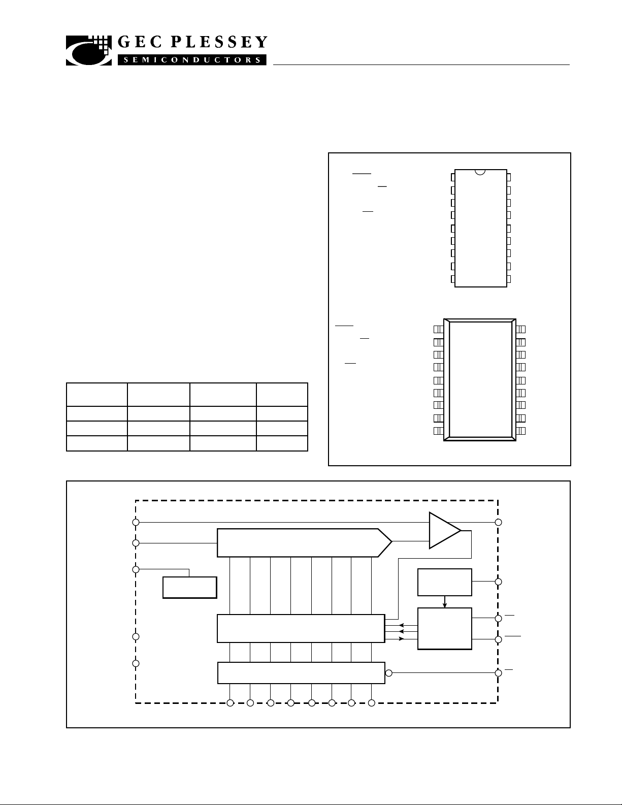
BUSY (END OF CONVERSION) DB0 (LSB)
RD (OUTPUT ENABLE) DB
CLOCK DB
WR (START CONVERSION)
R
EXT
V
IN
V
REF
IN DB
V
REF
OUT DB7 (MSB)
GROUND +V
181
172
1
163
2
154
DB
3
145
DB
4
136
DB
5
6
127
118
CC
109
(+5V)
ZN448/9E (DP18)
BUSY (END OF CONVERSION) DB0 (LSB)
RD (OUTPUT ENABLE) DB
CLOCK DB
WR (START CONVERSION)
R
EXT
V
IN
V
REF
IN DB
V
REF
OUT DB7 (MSB)
GROUND +V
181
172
163
154
145
136
127
118
109
DB
DB
DB
CC
1
2
3
4
5
6
(+5V)
ZN449D (MP18)
ANALOGUE
INPUT
V
REF
V
OUT
REF
GROUND
V
(+5V)
CC
Fig.1 Pin connection - top view
6
7
IN
8
2.5V
REFERENCE
9
10
11
DB
7
8-BIT DAC
SUCCESSIVE
APPROXIMATION REGISTER
3-STATE BUFFERS
DB
18171615141312
0
COMPARATOR
+
-
CLOCK
GENERATOR
INTERFACE
AND
CONTROL
LOGIC
5
3
4
1
2
R
EXT
CK RC OR
EXT CLOCK
WR
BUSY
RD
Fig.2 System diagram
ZN448/9
ABSOLUTE MAXIMUM RATINGS
Supply voltage VCC +7
Max. voltage, logic and VREF input +VCC
Operating temperature range 0°C to +70°C (MP and DP package)
Storage temperature range -55°C to +125°C
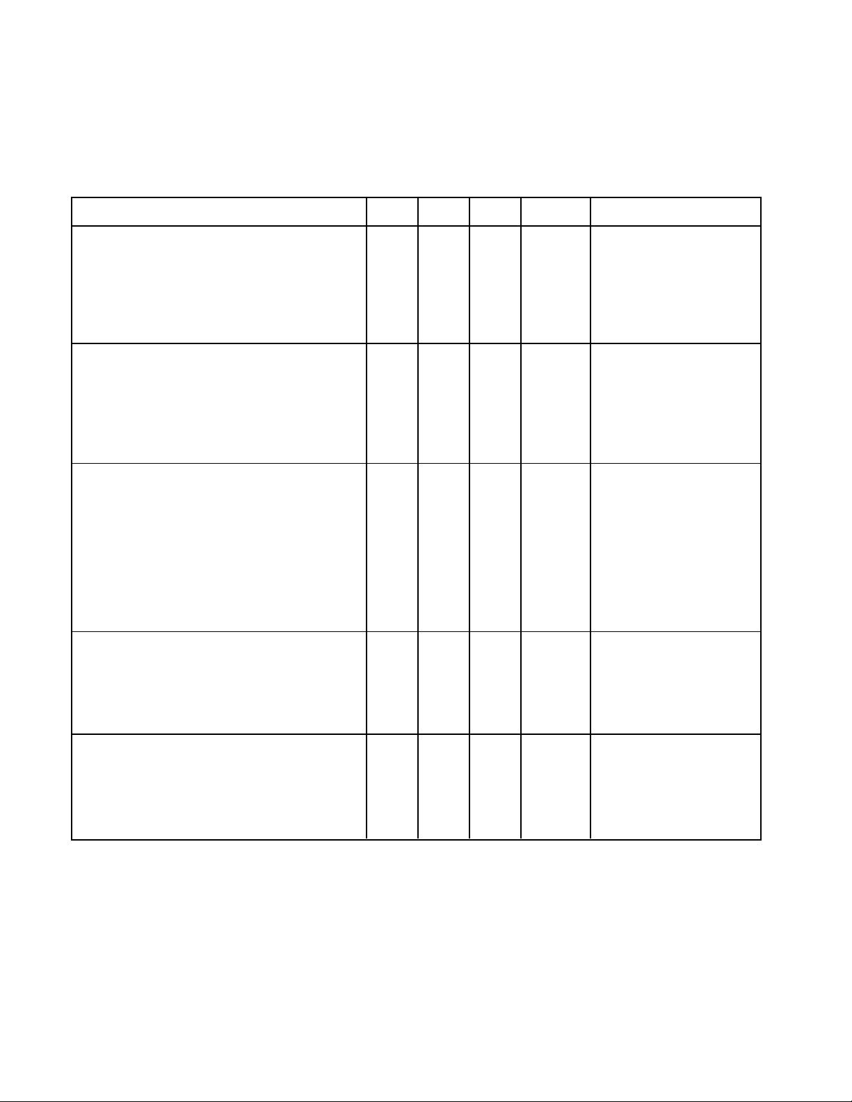
ELECTRICAL CHARACTERISTICS (at VCC = 5V, Tamb = 25°C and fCLK = 1.6MHz unless otherwise specified).
Parameter
ZN448
Linearity error
Differential linearity error
Zero transition
(00000000→00000001)
Full-scale→transition
(11111110 11111111)
ZN449
Linearity error
Differential linearity error
Zero transition
(00000000→00000001)
Full-scale→transition
(11111110 11111111)
All Types
Resolution
Linearity temperature coefficient
Differential linearity temperature coefficient
Full-scale temperature coefficient
Zero temperature coefficient
Reference input range
Supply voltage
Supply current
Power consumption
Min.
-
-
12
2.545
-
-
7
10
2.542
8
-
-
-
-
1
4.5
-
-
Typ. Max.
-
±0.5
-
±0.75
15
2.550
-
12
15
2.550
18
2.555
±1
±1
17
20
2.558
-
±3
±6
±2.5
±8
-
5
25
125
3
5.5
40
200
Units Conditions
LSB
LSB
mV
V
DP package
VREF = 2.560V
LSB
LSB
mV
mV
V
-
-
-
-
-
bits
ppm/°C
ppm/°C
ppm/°C
µV/°C
MP package
DP package
VREF = 2.560V
V
V
mA
mW
Comparator
Input current
Input resistance
Tail current
Negative supply
Input voltage
On-chip reference
Output voltage ZN448
ZN449
Slope resistance
V
temperature coefficient
REF
Reference current
2
-
-
25
-3
-0.5
2.520
2.520
-
-
4
1
100
65
-5
-
2.550
2.550
0.5
50
-
-
-
150
-30
+3.5
2.580
2.600
2
-
15
µA
kΩ
µA
V
V
V
Ω
ppm/°C
mA
VIN = +3V, R
V - = -5V
R
= 390Ω
REF
C
= 4µ7
REF
= 82kΩ
EXT
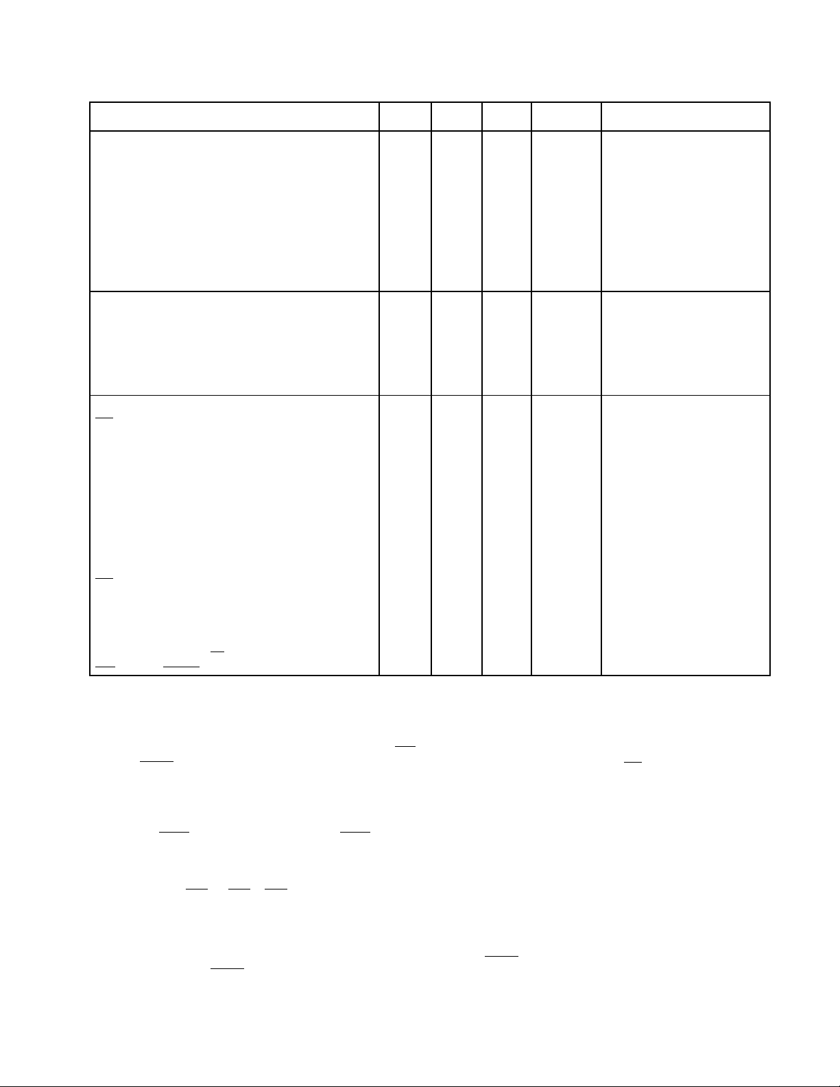
ELECTRICAL CHARACTERISTICS (Cont.)
ZN448/9
Parameter
Clock
On-chip clock frequency
Clock frequency temperature coefficient
Clock resistor
Maximum external clock frequency
Clock pulse width
High level input voltage V
Low level input voltage VIL
High level input current IIH
Low level input current IIL
Logic (over operating temperature range)
Convert input
High level input voltage VIH
Low level input voltage VIL
High level input current IIH
Low level input current IIL
RD input
High level input voltage VIH
Low level input voltage VIL
High level input current IIH
Low level input current IIL
High level output voltage VOH
Low level output voltage VOL
High level output current IOH
Low level output current IOL
Three-state disable output leakage
Input clamp diode voltage
RD input to data output
Enable/disable delay times T
Convert pulse width tWR
WR input to BUSY output
IH
E1
TE0
TD1
TD0
Min.
-
-
-
0.9
500
4
-
-
-
2
-
-
-
2
-
-
-
2.4
-
-
-
-
-
-
180
60
80
60
200
-
Typ. Max.
-
+0.5
-
-
-
-
-
-
-
-
300
±10
-
-
+150
-300
-
-
-
-
-
180
210
80
110
80
-
-
1
2
1
-
-
0.8
800
-500
-
0.8
-
-
-
0.8
-
-
-
0.4
-100
1.6
2
-1.5
250
260
100
140
100
-
250
Units Conditions
MHz
%/°C
kΩ
MHz
ns
V
V
µA
µA
V
= +4V, VCC = MAX
IN
VIN = +0.8V, VCC = MAX
V
V
µA
µA
VIN = +2.4V, VCC = MAX
VIN = +0.4V, VCC = MAX
V
V
µA
µA
V
V
VIN = +2.4V, VCC = MAX
VIN = +0.4V, VCC = MAX
IOH = +2.4V, VCC = MAX
IOL = +0.4V, VCC = MAX
µA
mA
µA
V
V
OUT
= +2V
ns
ns
ns
ns
ns
ns
ns
GENERAL CIRCUIT OPERATION
The ZN448/9 utilises the successive approximation
technique. Upon receipt of a negative-going pulse at the WR
input the BUSY output goes low, the MSB is set to 1 and all
other bits are set to 0, which produces an output voltage of
V
from the DAC. This is compared to the input voltage VIN;
REF/2
a decision is made on the next negative clock edge to reset the
V
MSB to 0 if < VIN or leave it set to 1 if < VIN.
REF
2
Bit 2 is set to 1 on the same clock edge, producing an output
from the DAC of or + depending on the state
V
REF
4
V
V
REF
REF
2
4
of the MSB. This voltage is compared to VIN and on the next
clock edge a decision is made regarding bit 2, whilst bit 3 is set
to 1. This procedure is repeated for all eight bits. On the eighth
negative clock edge BUSY goes high indicating that the
conversion is complete.
V
REF
2
During a conversion the RD input will normally be held high to
keep the three-state buffers in their high impedance state.
Data can be read out by taking RD low, thus enabling the
three-state output. Readout is non-destructive.
CONVERSION TIMING
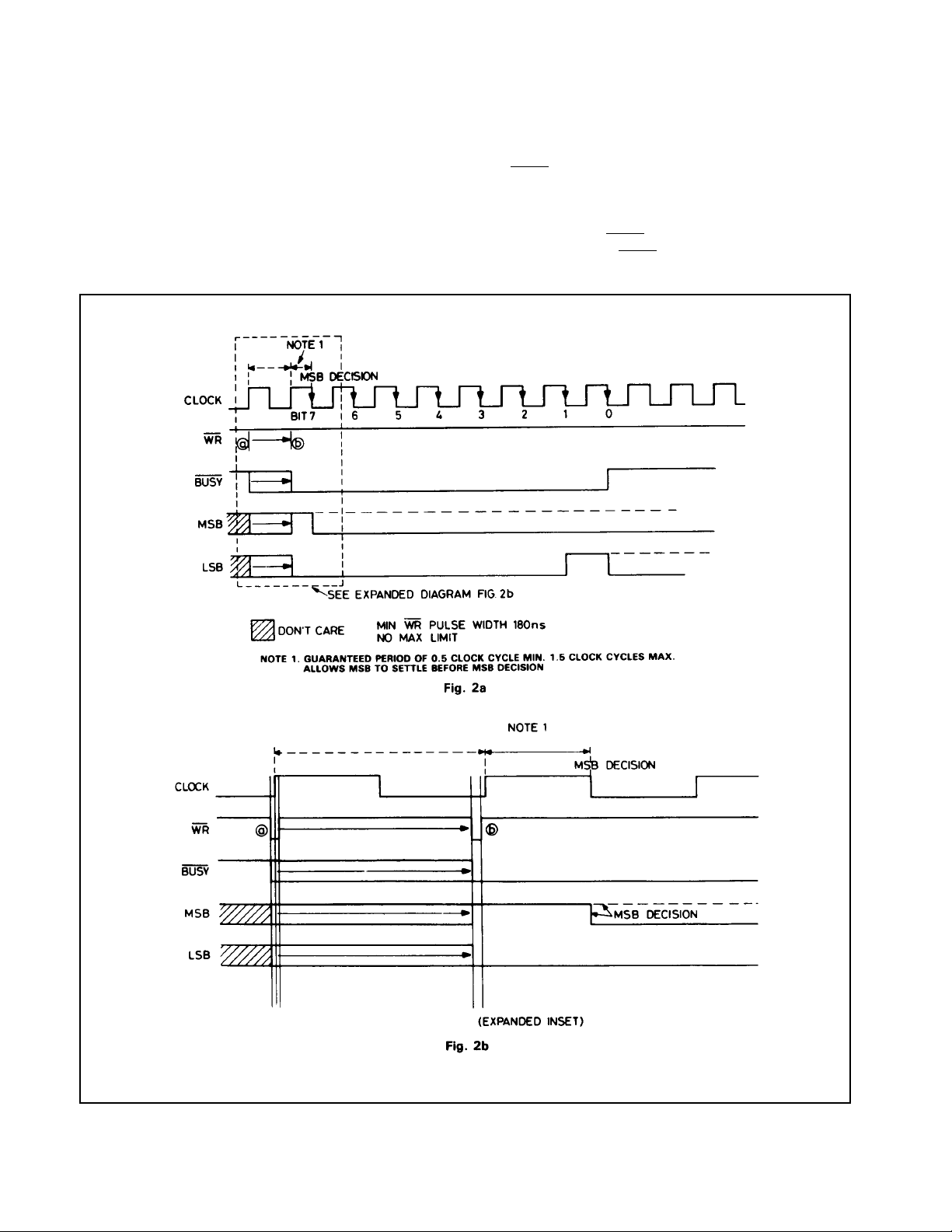
The ZN448/9 will accept a low-going CONVERT pulse, which
can be completely asynchronous with respect to the clock,
and will produce valid data between 7.5 and 8.5 clock pulses
later depending on the relative timing of the clock and
CONVERT signals. Timing diagrams for the conversion are
shown in Fig.3.
The converter is cleared by a low-going CONVERT pulse,
which sets the most significant bit and results all the other bits
and the BUSY flag. Whilst the CONVERT input is low the MSB
output of the DAC is continuously compared with the analogue
input, but otherwise the converter is inhibited.
3
ZN448/9
After the CONVERT input goes high again the MSB decision
is made and the successive approximation routine runs to
completion.
The CONVERT pulse can be as short as 200ns; however the
MSB must be allowed to settle for at least 550ns before the
MSB decision is made. To ensure that this criterion is met
even with short CONVERT pulses the converter waits, after
the CONVERT input goes high, for a rising clock edge followed
by a falling clock edge, the MSB decision being taken on the
falling clock edge. This ensures that the MSB is allowed to
settle for at least half a clock period, or 550ns at maximum
clock frequency. The CONVERT input is not locked out during
a conversion and if it is oulsed low at any time the converter
will restart.
The BUSY output goes high simultaneously with the LSB
decision, at the end of a conversion indicating data valid. Note
that if the three-state data outputs are enabled during a
conversion the valid data will be available at the outputs after
the rising edge of the BUSY signal. If, however the outputs are
not enabled until after BUSY goes high then the data will be
subject to the propagation delay of the three-state buffers.
(See under DATA OUTPUTS).
Fig.3 ZN448/9 timing diagram
4
ZN448/9
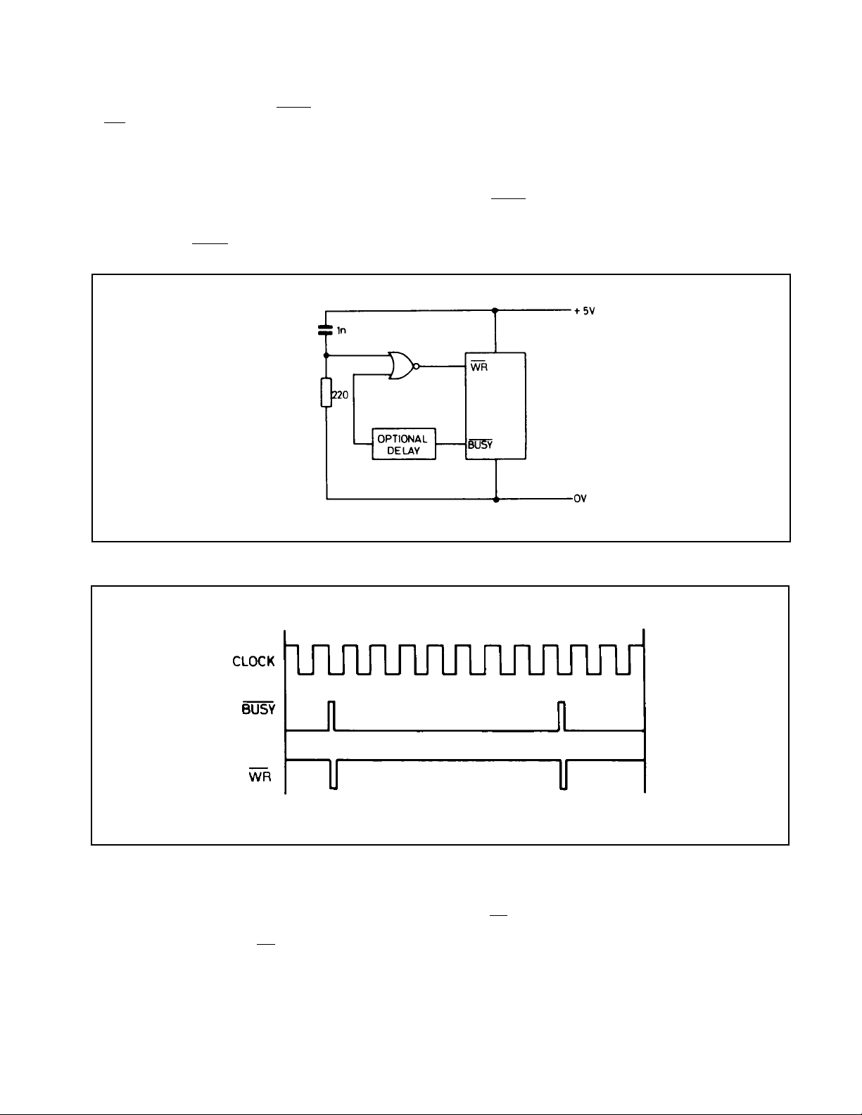
If a free-running conversion is required, then the converter can
be made to cycle by inverting the BUSY output and feeding it
to WR. To ensure that the converter starts reliably after powerup an initial start pulse is required. This can be ensured by
using a NOR gate instead of an inverter and feeding it with a
positive-going pulse which can be derived from a simple RC
network that gives a single pulse when power is applied, as
shown in Fig.4a.
The ADC will complete a conversion on every eighth clock
pulse, with the BUSY output going high for a period
determined by the propagation delay of the NOR gate, during
which time the data can be stored in a latch. The time available
for storing data can be increased by inserting delays into the
inverter path.
A timing diagram for the continuous conversion mode is
shown in Fig.3b.
As the BUSY output uses a passive pull-up the rise time of this
output depends on the RC time constant of the pull-up resistor
and load capacitance. In the continuous conversion mode the
use of a 4k7 external pull-up resistor is recommended to
reduce the risetime and ensure that a logic 1 level is reached.
Fig.4a Circuit for continuous conversion
Fig.4b Timing for continuous conversion
DATA OUTPUTS
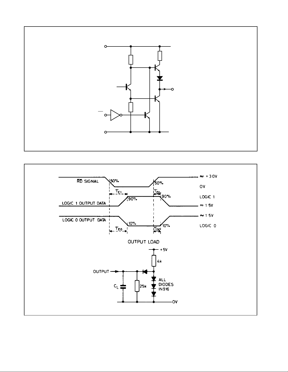
The data outputs are provided with three-state buffers to allow
connection to a common data bus. An equivalent circuit is
shown in Fig.5. Whilst the RD input is high both output
transistors are turned off and the ZN448/9 presents only a high
impedance load to the bus.
RD is low the data outputs will assume the logic states
When
present at the outputs of the successive register.
A test circuit and timing diagram for the output enable/disable
delays are given in Fig.6.
5
ZN448/9
RD
(PIN 2)
GROUND
V
CC
500Ω
20k
BITS 1-8
(PINS 11-18)
10k
Fig.5 Data output
Fig.6 Output enable/disable delays
6
 Loading...