THIS DOCUMENT IS FOR MAINTENANCE
PURPOSES ONLY AND IS NOT
RECOMMENDED FOR NEW DESIGNS

DP14
1
2
3
4
5
6
7
BIT 6
BIT 8 (LSB)
9
10
BIT 2
(MSB) BIT 1
ANALOG OUTPUT
V
REF
IN
BIT 7
NC
0V
11
12
13
14
BIT 3
BIT 4
BIT 5
+V
CC
(+5V)
NC
1
2
3
4
5
6
7
8
BIT 6
BIT 8
9
10
BIT 3
BIT 2
BIT 1
ANALOG OUTPUT
BIT 7
V
REF
IN
+V
CC
11
12
13
14
GROUND
NC
BIT 4
BIT 5
GROUND
8
ZN429E8
ZN429D
MP14
■
■
■
■
■
■
MAY 1994
DS3008-2.0
ZN429E8/ZN429D
LOW COST 8-BIT D-A CONVERTER
The ZN429 is a monolithic 8-bit D-A converter
containing an R-2R ladder network of diffused resistors with
precision bipolar switches.
FEATURES
Linearity Error ±
Single +5V Supply
Low Power Consumption 25mW Typical
Settling Time 1 Microsecond Typical
TTL and 5V CMOS Compatible
Designed for Low Cost Applications
1
/
2
LSB
ABSOLUTE MAXIMUM RATINGS
Supply voltage, V
Max. voltage, logic and V
Storage temperature range -55 ° C to +125 ° C
CC
ORDERING INFORMATION
Ambient operating temperature -40 ° C to +85 ° C
Package, ZN429D MP14
Package, ZN429E8 DP14
inputs +5.5V
REF
+7.0V
Fig.1 Pin connections (not to scale) - top view

µ V/ °
±
±
µ
µ
ZN429
ELECTRICAL CHARACTERISTICS
(at T
= 25 ° C and V
amb
= +5V unless otherwise specified)
CC
µ
Parameter Symbol
Min. Typ. Max.
Units Conditions
Converter
Resolution 8 - - bits
Accuracy 8 - - bits
Non-linearity - Differential non-linearity -
0.5 - LSB Note 1
Settling time to 0.5LSB - 1.0 Settling time to 0.5LSB - 2.0 -
0.5 LSB
s 1 LSB step
s All bits ON to OFF
or OFF to ON
Offset voltage ZN429E8, ZN429D V
V
temperature coefficient - 5 -
OS
OS
- 3.0 5.0 mV All bits OFF
C
Full-scale output 2.545 2.550 2.555 V All bits ON
Ext. V
Full-scale temp. coefficient - 3 - ppm/ ° C Ext. V
= 2.56V
REF
= 2.560V
REF
Non-linearity temp. coefficient - 7.5 - ppm/ ° C Relative to F.S.R.
Analog output resistance R
O
-10- k
Ω
External reference voltage 0 - 3.0 V
Supply voltage V
Supply current I
High level input voltage V
Low level input voltage V
High level input current I
CC
S
IH
IL
IH
4.5 - 5.5 V
-59mA
2.0 - - V
- - 0.7 V
--10
- - 100
Low level input current I
IL
- - -0.18 mA V
NOTE 1: Monotonic over full temperature range.
INTRODUCTION
The ZN429 is an 8-bit D-A converter. It contains an
advanced design of R-2R ladder network and an array of
precision bipolar switches on a single monolithic chip.
The special design of the ladder network results in full
8-bit accuracy using normal diffused resistors.
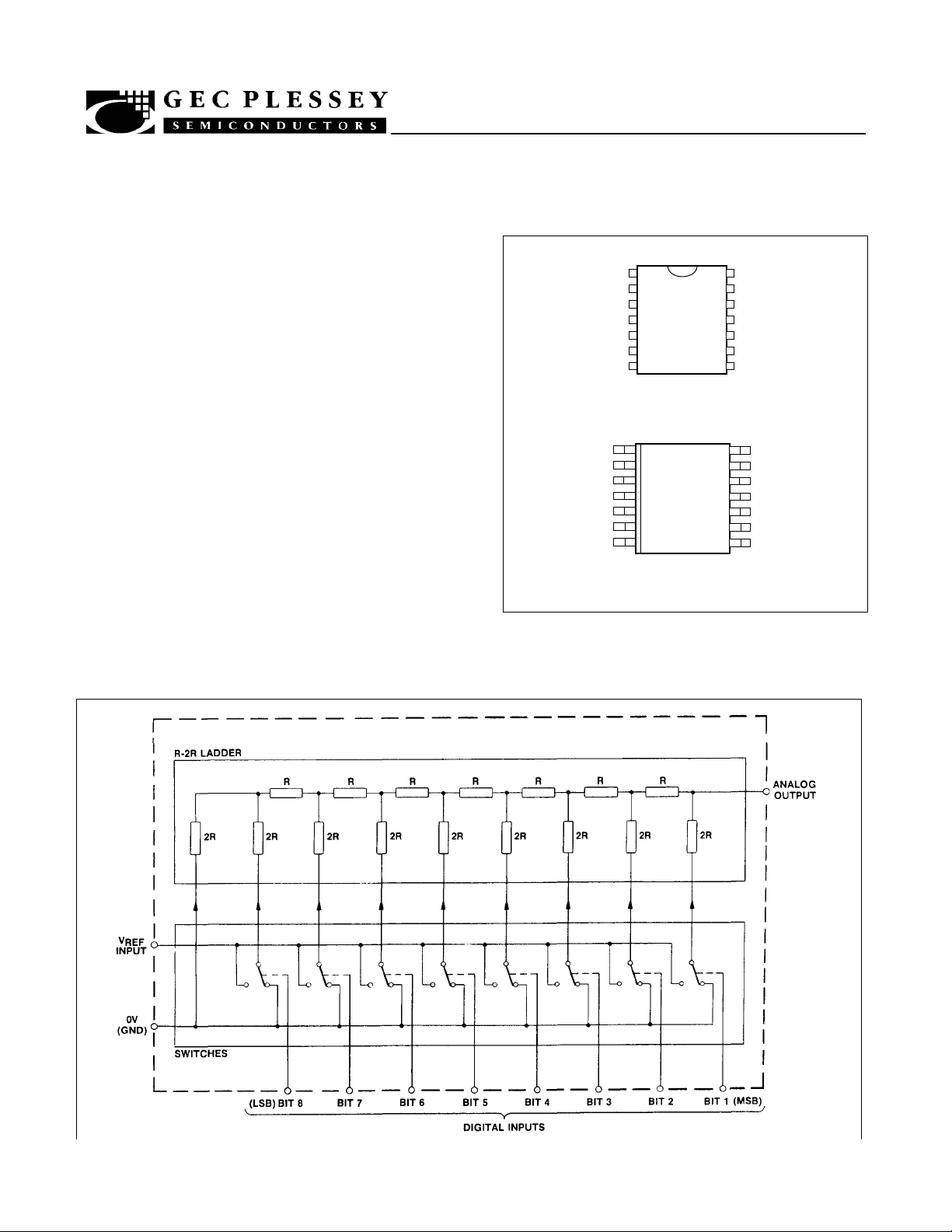
The converter is of the voltage switching type and uses
an R-2R resistor ladder network as shown in Fig.3.
Each 2R element is connected either to 0V or V
transistor switches specially designed for low offset voltage
(typically 1mV).
REF
by
µ
AV
AV
CC
V
= 2.4V
I
CC
V
= 5.5V
I
CC
V
= 0.3V
I
= max.
= max.
= max.
Binary weighted voltages are produced at the output of
the R-2R ladder, the value depending on the digital number
applied to the bit inputs.
An external fixed or varying reference is required which
should have a slope resistance less than 2 Ω .
Suggested external reference sources are the ZN404 or
one of the ZN458 range. Each ZN404 is capab le of supplying
up to five ZN429 circuits and this is increased to ten for the
ZN458 range.
 Loading...