GEC Plessey Semiconductors ZN428D, ZN428E8, ZN428J8 Datasheet

THIS DOCUMENT IS FOR MAINTENANCE
PURPOSES ONLY AND IS NOT
RECOMMENDED FOR NEW DESIGNS

DC16
1
2
3
4
5
6
7
BIT 3
BIT 1 (MSB)
9
10
BIT 8
NC
ANALOG OUTPUT
V
REF
IN
BIT 2
V
REF
OUT
ANALOG GROUND
11
12
13
14
BIT 7
BIT 5
BIT 4
BIT 6
+V
CC
(+5V)
1
2
3
4
5
6
7
8
9
10
11
12
13
14
15
16
ZN428J8
ZN428D
MP16 WIDE BODY
8
15
16
ENABLE
DIGITAL GROUND
ZN428E8
DP16
BIT 8
NC
ANALOG OUTPUT
V
REF
IN
V
REF
OUT
ANALOG GROUND
BIT 7
ENABLE
BIT 3
BIT 1 (MSB)
BIT 2
BIT 5
BIT 4
BIT 6
+V
CC
(+5V)
DIGITAL GROUND
■
■
■
■
■
■
■
■
AUGUST 1994
DS3007-2.1
ZN428E8/ZN428J8/ZN428D
8-BIT LATCHED INPUT D-A CONVERTER
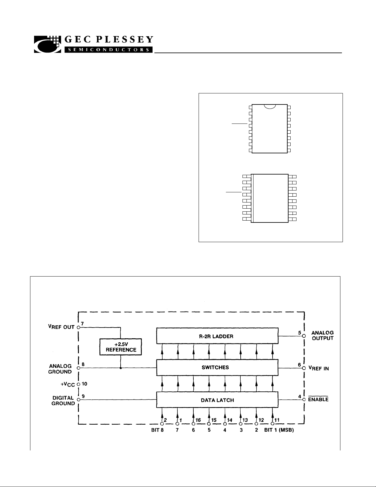
The ZN428 is a monolithic 8-bit D-A converter with input
latches to facilitate updating from a data bus. The latch is
transparent when enable is LOW and the data is held when
enable is taken HIGH. The ZN428 also contains a 2.5V
reference the use of which is pin optional to retain flexibility.
An external fixed or varying reference may therefore be
substituted.
FEATURES
Contains DAC with Data Latch and On-Chip
Reference
Guaranteed Monotonic over the Full Operating
Temperature Range
Single +5V Supply
Microprocessor Compatible
TTL and 5V CMOS Compatible
800ns Settling Time
Complementary to ZN427 A to D Series
Commercial or Military Temperature Range
ORDERING INFORMATION
Device Type Operating temperature Package
ZN428D 0 ° C to +70 ° C MP16W
ZN428E8 0 ° C to +70 ° C DP16
ZN428J8 -55 ° C to +125 ° C DC16
Fig.1 Pin connections (not to scale) - top view

±
≤
±
±
±
Ω
±
° C °
µ
±
ZN428
ABSOLUTE MAXIMUM RA TINGS
Supply voltage V
Max.voltage, logic and V
Operating temperature range 0 ° C to +70 ° C (ZN428E8, ZN428D)
CC
inputs +V
REF
Storage temperature range -55 ° C to +125 ° C
Analog ground to digital ground
ELECTRICAL CHARACTERISTICS
(V
= +5V, T
CC
= 25 ° C unless otherwise specified)
amb
+7.0V
CC
-55 ° C to +125 ° C (ZN428J8)
200mV
Parameter
Min. Typ. Max.
Units Conditions
Internal V oltage Reference
Output voltage 2.475 2.550 2.625 V
Slope resistance - 0.5 2
V
REF OUT
T .C . - 50 - ppm/ ° C
123
R
C
REF
REF
= 390 Ω
= 1 µ F
Reference current 4 - 15 mA Note 1
D-A Converter
Linearity error - Differential non-linearity Linearity error T.C. Differential non-linearity T.C. -
0.5 - LSB
3 - ppm/ ° C
6 - ppm/ ° C
0.5 LSB 2.0V ≤ V
Offset voltage - 2 5 mV All bits off
Offset voltage T.C. Full-scale output 2.545 2.550 2.555
Full-scale output T.C. - 2 - ppm/ ° C
6-
µ
V/ ° C
External reference
V
REF
123
all bits ON
Analog output resistance - 4 - k Ω
REF IN
= 2.560V,
IN
3.0V
External reference voltage 0 - 3.0 V
Settling time to 0.5 LSB -
800
-
ns
1 LSB major transition
(Note 2)
-
1.25
-
s
All bits ON to OFF or
OFF to ON (Note 2)
Operating temperature range:
ZN428D and ZN428 E8
Supply voltage (V
ZN428J8
) 4.5 5.0 5.5 V
CC
0
-55
-
-
70
125
C
Supply current - 20 30 mA Note 3
Power consumption - 100 - mW
Note 1: See REFERENCE
Note 2: R
Note 3: All inputs HIGH (V
= 10M Ω , C
L
= 10pF
L
IH
= 3.5V)
 Loading...