

GEC Plessey Semiconductors ZN427E8, ZN427J8 Datasheet

THIS DOCUMENT IS FOR MAINTENANCE
PURPOSES ONLY AND IS NOT
RECOMMENDED FOR NEW DESIGNS
ZN427E8 / ZN427J8
WR (START CONVERSION)
BUSY (END OF CONVERSION) BIT 8 (LSB)
RD (OUTPUT ENABLE) BIT 7
CLOCK BIT 6
BIT 5
R
EXT
BIT 4
V
IN
BIT 3
V
REF
IN BIT 2
V
REF
OUT BIT 1 (MSB)
GROUND +V
CC
(+5V)
181
172
163
154
145
136
127
118
109
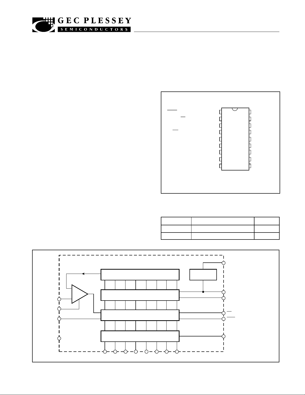
MICROPROCESSOR COMPATIBLE
8-BIT SUCCESSIVE APPROXIMATION A-D CONVERTER
The ZN427 is an 8-bit successive approximation converter
with three-state outputs to permit easy interfacing to a
common data bus. The IC contains a voltage switching DAC,
a fast comparator, successive approximation logic and a
2.56V precision bandgap reference, the use of which is pin
optional to retain flexibility. An external fixed or varying
reference may therefore be substituted, thus allowing
ratiometic operation
Only passive external components are required for
operation of the converter.
FEATURES
■ Easy Interfacing to Microprocessor, or Operates as a
'Stand-Alone' Converter
■ Fast: 10 microseconds Conversion time Guaranteed
■ No Missing Codes over Operating Temperature Range
■ Data Outputs Three-State TTL Compatible, other
Logic Inputs and Output TTL and CMOS Compatible
■ Choice of On-Chip or External Reference Voltage
■ Ratiometric Operation
■ Unipolar or Bipolar Input Ranges
■ Complementary to ZN428 DAC
■ Commercial or Military Temperature Range
ZN427J8 (DC18)
ZN427E8 (DP18)
Fig.1 Pin connection - top view
ORDERING INFORMATION
Device type
ZN427E8
ZN427J8
0°C to +70°C
-55°C to +125°C
DS3006 - 2.1
PackageOperating temperature
DP18
DC18
D TO A OUTPUT
COMPARATOR
-
6
V
IN
R
EXT
CLOCK
INPUT
V
CC
(+5V)
+
5
3
10
MSB
R-2R LADDER
ANALOGUE VOLTAGE SWITCHES
SUCCESSIVE
APPROXIMATION REGISTER
3-STATE BUFFERS
11
Fig.2 System diagram
LSB
8
V
OUT
REF
+2.5V
REFERENCE
9
GROUND
7
V
IN
REF
4
WR (START CONVERSION)
1
BUSY (END CONVERSION)
2
RD (OUTPUT ENABLE)
18171615141312
ZN427
ABSOLUTE MAXIMUM RATINGS
Supply voltage VCC +7.0V
Max. voltage, logic and VREF input +VCC
Operating temperature range 0°C to +70°C (ZN427E8)
-55°C to +125°C (ZN427J8)
Storage temperature range -55°C to +125°C
ELECTRICAL CHARACTERISTICS (at VCC = 5V, Tamb = 25°C unless otherwise specified).
Parameter
Converter
Resolution
Linearity error
Differential non-linearity
Linearity error T.C.
Differential non-linearity T.C.
Full-scale (gain) T.C.
Zero T.C.
Zero transition 00000000
to 00000001
F.S. transition 11111110
to 11111111
Conversion time
External reference voltage
Supply voltage (VCC)
Supply current
Power consumption
Min.
12
10
2.545
1.5
4.5
8
-
-
-
-
-
-
-
-
-
Typ. Max.
-
-
±0.5
±3
±6
±2.5
±8
15
13
2.550
-
-
-
25
125
-
±0.5
-
-
-
-
18
16
2.555
10
3.0
5.5
40
-
Units Conditions
Bits
LSB
LSB
ppm/°C
ppm/°C
ppm/°C
µV/°C
mV
mV
V
µs
V
V
mA
mW
External Ref. 2.5V
DC Package
DP Package
V
= 2.560V
REF IN
See note 1
Comparator
Input current
Input resistance
Tail current, I
Negative supply, V–
EXT
Input voltage
-
-
25
-3.0
-0.5
1
100
-
-
-
Internal voltagee reference
Output voltage
Slope resistance
V
temperature coefficient
REF
Reference current
2.475
-
-
4
2.560
0.5
50
-
Logic (over operating temperature range)
High level input voltage VIH
Low level input voltage VIL
High level input current,
WR and RD inputs I
High level input current,
Clock input I
Low level input current IIL
IH
IH
High level output current IOH
Low level output current IOL
High level output voltage VOH
Low level output voltage VOL
Disable output leakage
Input clamp diode voltage
Read input to data output
Enable/disable delay time t
Start pulse width tWR
RD
WR to BUSY propagation delay t
Clock pulse width
Maximum clock frequency
BD
2.0
-
-
-
-
-
-
-
-
2.4
-
-
-
-
-
250
500
900
-
-
-
-
-
-
-
-
-
-
-
-
-
180
160
-
-
1000
Note 1: A 900kHz clock gives a conversion time of 10µs (9 clock periods).
-
-
15
-30.0
3.5
2.625
2
-
15
-
0.8
50
15
100
30
-5
-100
1.6
-
0.4
2
-1.5
250
250
-
250
-
-
µA
kΩ
µA
V
V
V
Ω
ppm/°C
mA
V
V
µA
µA
µA
µA
µA
µA
mA
V
V
µA
V
ns
ns
ns
ns
ns
kHz
VIN = +3V, R
V - = -5V
= 82kΩ
EXT
See comparator (page x-xx)
R
= 390Ω, C
REF
REF
= 4µ7
See reference (page x-xx)
VIN = 5.5V, VCC = max.
VIN = 2.4V, VCC = max.
VIN = 5.5V, VCC = max.
VIN = 2.4V, VCC = max.
VIN = 0.4V, VCC = max.
IOH = max., VCC = min.
IOL = max., VCC = min.
VO = 2.4V
See Fig.9
See Fig.9
See note 1
2
ZN427
GENERAL CIRCUIT OPERATION
The ZN427 utilises the successive approximation technique.
Upon receipt of a negative-going pulse at the WR input the
BUSY output goes low, the MSB is set to 1 and all other bits
are set to 0, which produces an output voltage of V
DAC. This is compared to the input voltage VIN; a decision is
made on the next negative clock edge to reset the
V
MSB to 0 if > VIN or leave it set to 1 if < VIN.
REF
2
Bit 2 is set to 1 on the same clock edge, producing an output
from the DAC of or + depending on the state
V
REF
4
V
V
REF
REF
2
4
of the MSB. This voltage is compared to VIN and on the next
clock edge a decision is made regarding bit 2, whilst bit 3 is set
REF/2
V
from the
REF
2
to 1. This procedure is repeated for all eight bits. On the ninth
negative clock edge BUSY goes high indicating that the
conversion is complete.
During a conversion the RD input will normally be held high to
keep the three-state buffers in their high impedance state.
Data can be read out by taking RD high, thus enabling the
three-state output. Readout is non-destructive. The BUSY
output may be tied to the RD input to automatically enable the
outputs when the data is valid.
For reliable operation of the converter the start pulse applied
to the WR input must meet certain timing criteria with respect
to the converter clock. These are detailed in the timing
diagram of Fig.3.
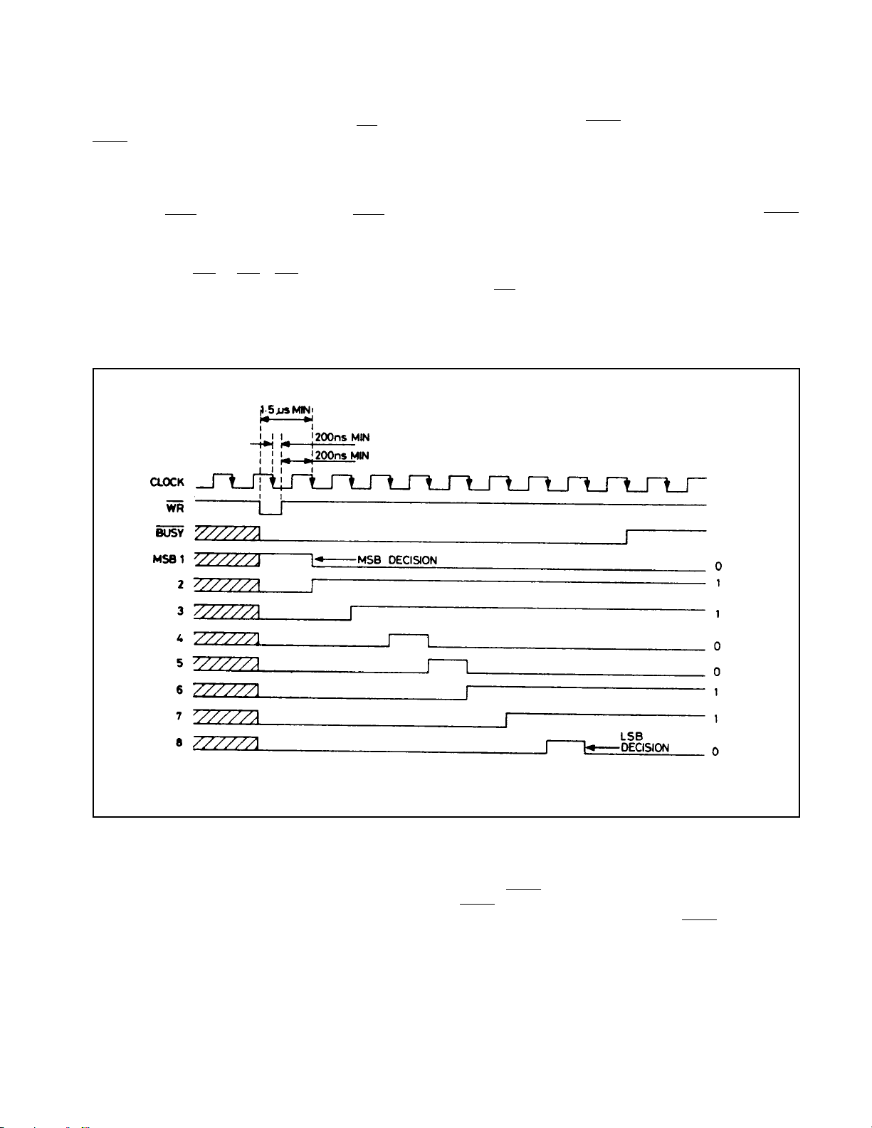
Fig.3 Timing diagram
NOTES ON TIMING DIAGRAM
1. A conversion sequence is shown for the digital word
01100110. For clarity the three-state outputs are shown as
being enabled during the conversion, but normal practice
would be to disable them until the conversion was complete.
2. The BUSY output goes low during a conversion. When
BUSY goes high at the end of a conversion the output data is
valid. In a microprocessor system the BUSY output can be
used to generate an interrupt request when the conversion is
complete.
3
ZN427
3. In the timing diagram cross hatching indicates a 'don't
care' condition.
4. The start pulse operates as an asynchronous
(independent of clock) reset that sets the MSB output to 1 and
sets all other outputs and the end of conversion flag to 0. This
resetting occurs on the low-going edge of the start pulse and
as long as WR is low the converter is inhibited. Conversion
commences on the first active (negative going) clock edge
after the WR input has gone high again, when the MSB
decision is made. A number of timing constraints thus supply
to the start pulse.
(a) The minimum duration of the start pulse is 250ns, to allow
reliable resetting of the converter logic circuits.
(b) There is no limit to the maximum duration of the start pulse.
(c) To allow the MSB to settle at least 1.5µs must elapse
between the negative going edge of the start pulse and the first
active clock edge that indicates the MSB desicion.
(d) To ensure relaible clocking the positive-going edge of the
start pulse should not occur within 200ns of an active
(negative-going) clock edge. The ideal place for the positivegoing edge of the start pulse is coincident with a positive-going
clock edge. As a special case of the above conditions that
start pulse may be synchronous with a negative-going clock
pulse.
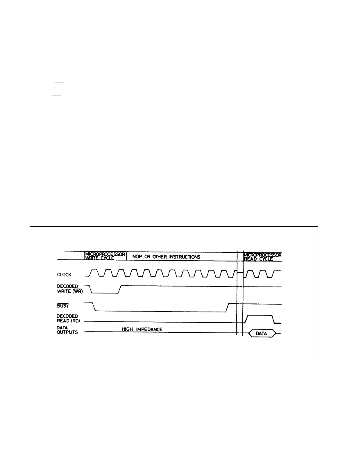
PRACTICAL CLOCK AND SYNCHRONISING
CIRCUITS
The actual method of generating the clock signal and
synchronising it to the start conversion system in which the
ZN427 is incorporated.
When used with a microprocessor the ZN427 can be treated
as RAM and can be assigned a memory address using an
address decoder. If the µP clock is used to drive the ZN427
and the µP write pulse meets the ZN427 timing criteria with
respect to the µP clock then generating the start pulse is
simply a matter of gating the decoded address with the
microprocessor write pulse. Whilst the conversion is being
performed the microprocesor can perform other instructions
or No operation (NOP). when the conversion is complete the
outputs can be enabled onto the bus by gating the decoded
address with the read pulse. A timing diagram for this
sequence of operation is given in Fig.4.
An advantage of using the microprocessor clock is that the
conversion time is known precisely in terms of machine
cycles. the data outputs may therefore be read after a fixed
delay of at least nine clock cycles after the end of the WR
pulse, when the conversion will be complete.
Alternatively the read operation may be initiated by using the
BUSY output to generate interrupt request.
Fig.4 Typical timing diagram using µP clock and write pulse
In some systems, for example single-chip microcomputers
such as the 8048, this simple method may not be feasible for
one or more of the following reasons:
4
(a) The MPU clock is not available externally.
(b) The clock frequency is too high.
ZN427
(c) The write pulse timing criteria make it unsuitable for direct
use as a start conversion pulse.
If any of these conditions apply then the self-synchronising
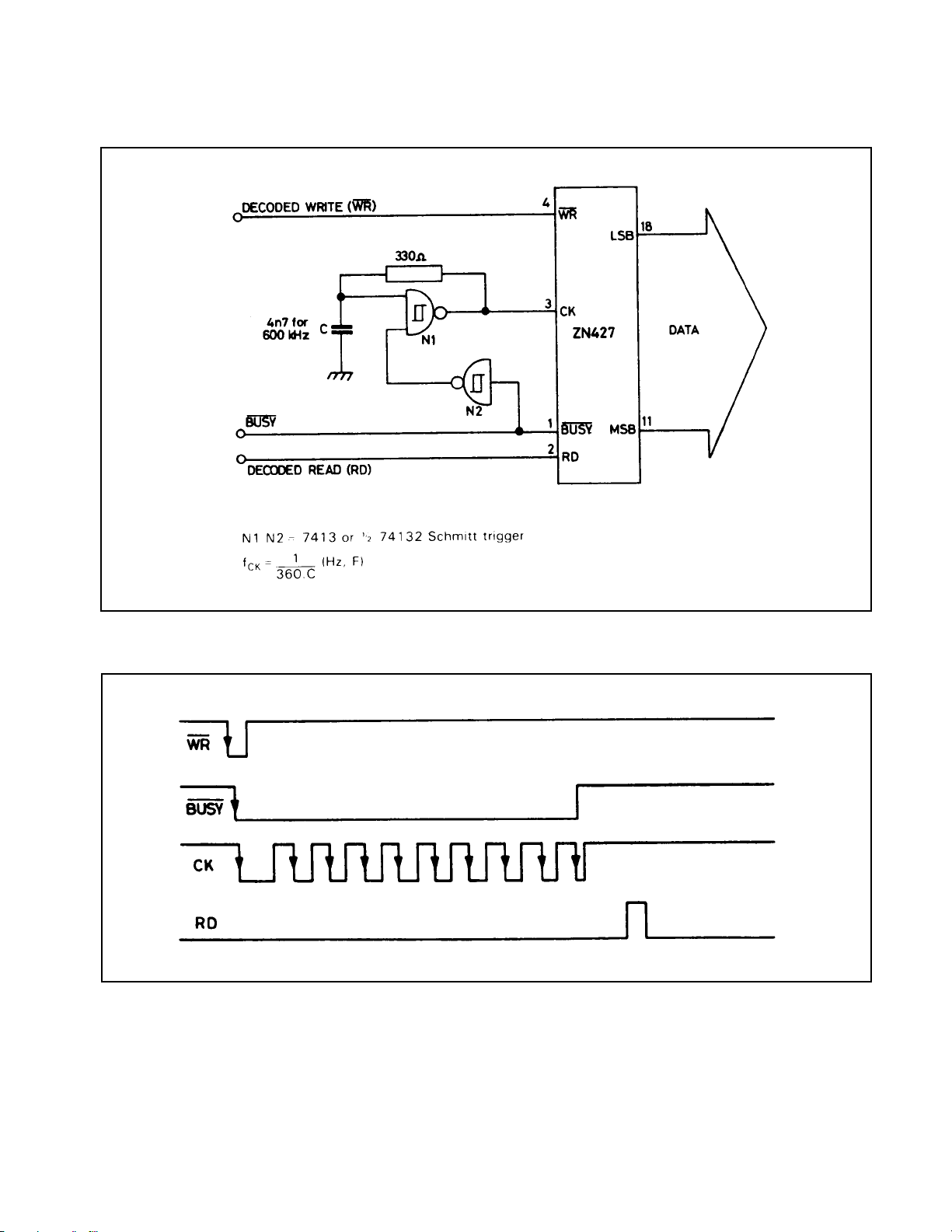
clock circuit of Fig.5a is recommended.
Fig.5a Self-synchronising clock circuit
Fig.5b Timing diagram for circuit of Fig.5a
5
 Loading...