GEC Plessey Semiconductors SP8792, SP8793 Datasheet

THIS DOCUMENT IS FOR MAINTENANCE
PURPOSES ONLY AND IS NOT
RECOMMENDED FOR NEW DESIGNS

SP8792 225MHz ÷ 80/81
SP8793 225MHz ÷ 40/41
WITH ON-CHIP VOLTAGE REGULATOR
The SP8792 AND SP8793 are low power programmable
÷80/81 and ÷40/41 counter, temperature range: -40°C to
+85°C.They divide by 80(40) when control input is in the high
state and by 81(41) when in the low state. An internal voltage
regulator allows operation from a wide range of supply
voltages.
FEATURES
Very Low Power
Control Input and Output CMOS/TTL Compatible
AC Coupled Input
Operation up to 9.5V using Internal Regulator
QUICK REFERENCE DATA
Supply Voltage 5.2V or 6.8V to 9.5V
Power consumption: 26mW Typical
DS 3294- 1
MODULUS CONTROL INPUT 1 Vcc 18
OUTPUT Vcc 2 2 Vcc 27
OUTPUT 3 INTERNAL DECOUPLING6
0V) 4 INPUT5
DP8
MP8
Figure 1 Pin connections - top view
ABSOLUTE MAXIMUM RATINGS
Supply voltage 6.0V pins 7 & 8 tied
Supply voltage 13.5V pin 8, pin 7 decoupled
Storage temperature range -55°C to +125°C
Max. Junction temperature +175°C
Max. clock input voltage 2.5V p-p
Vcc2 max. 10V
CLOCK
INPUT
1n
1n
DECOUPLING
VCC1
VCC2
2
5
6
VEE (0V)
DIVIDE BY 80/81
DIVIDE BY 40/41
4
(SP8792)
(SP8793)
16k
13
CONTROL
INPUT
OUTPUT
100n
8
VOLTAGE
REGULATOR
7
100n
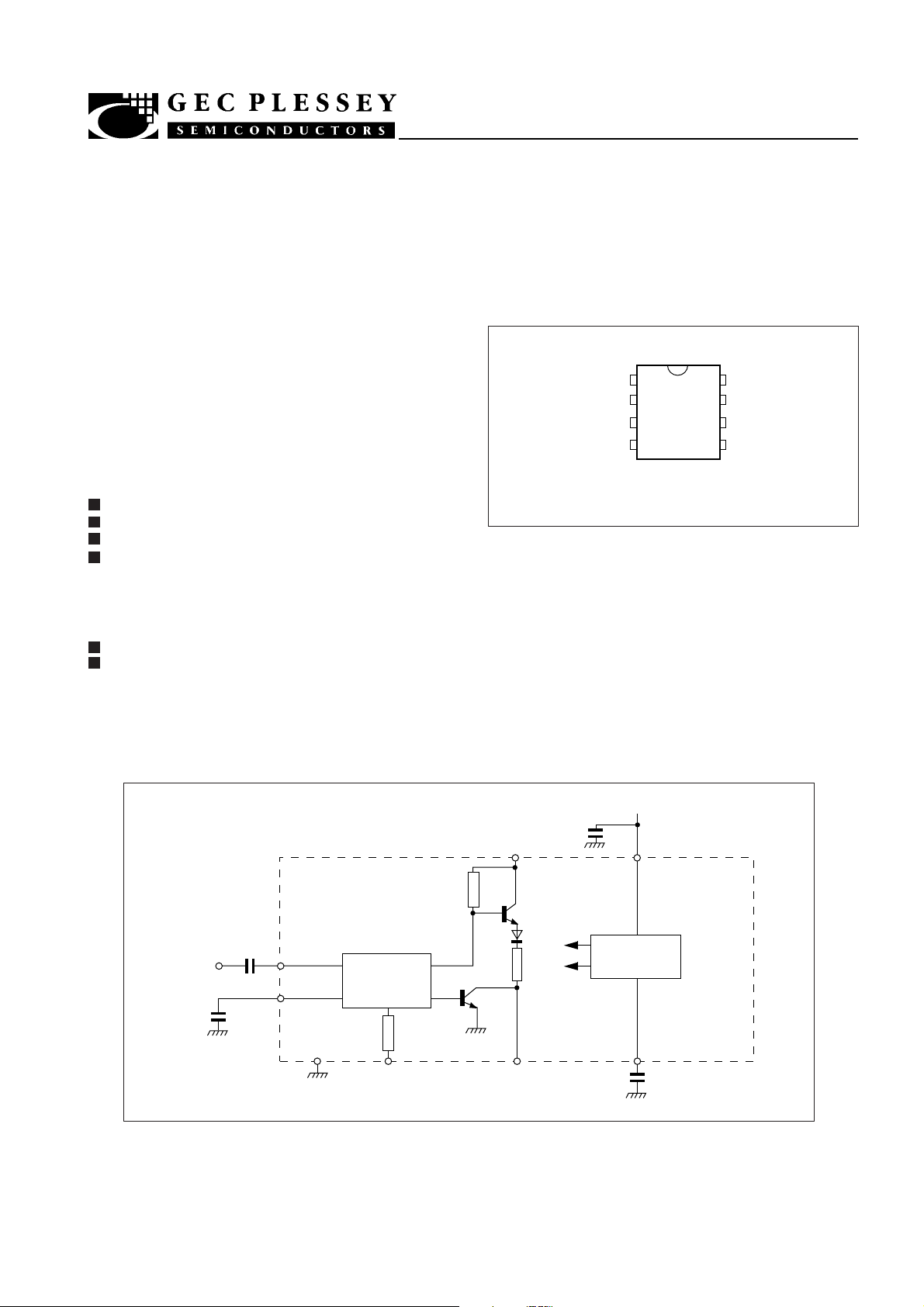
Figure 2 : Functional diagram SP8799
 Loading...