GEC Plessey Semiconductors SL560CCM, SL560CDP Datasheet

THIS DOCUMENT IS FOR MAINTENANCE
PURPOSES ONLY AND IS NOT
RECOMMENDED FOR NEW DESIGNS

SL560
300MHz LOW NOISE AMPLIFIER
This monolithic circuit contains three very high performance
transistors and associated biasing components in an eightlead TO-5 package forming a 300MHz low noise amplifier. The
configuration employed permits maximum flexibility with
minimum use of external components. The SL560C is a
general purpose low noise, high frequency gain block.
The device is also available as the SL560AC which has
guaranteed operation over the fully Military Temperatures
Range and is screened to MIL-STD-883 Class B. Data is
available separately.
FEATURES
■ Gain up to 40dB
■ Noise Figures less than 2dB (Rs 200 ohm)
■ Bandwidth 300MHz
■ Supply Voltage 2-15V (Depending on Configuration)
■ Low Power Consumption
APPLICATIONS
■ Radar IF Preamplifiers
■ Infra-Red Sysems Head Amplifiers
■ Amplifiers in Noise Measurement Systems
■ Low Power Wideband Amplifiers
■ Instrumentation Preamplifiers
■ 50 ohm Line Drivers
■ Wideband Power Amplifiers
■ Wideband Dynamic Range IF Amplifiers
■ Aerial Preamplifiers
ABSOLUTE MAXIMUM RATINGS
Supply voltage +15V
Storage temperature
SL560C DP -55°C to +150°C
SL560C CM -65°C to +150°C
Junction temperature
SL560C DP +150°C
SL560C CM +175°C
Operating temperature range
SL560C DP -30°C to +85°C
SL560C CM -55°C to +125°C
Thermal resistance
Chip-to-ambient
SL560C CM 225°C/W
SL560C DP 111°C/W
Chip-to-case
SL560C CM 65°C/W
SL560C DP 71°C/W
ADVANCE INFORMATION
INPUT
GAIN SET
50 APPLICATIONS
8
71
6
SL560
53
4
Vcc
INPUT
COMMON BASE
CONFIGURATION
INPUT
COMMON EMITTER
CONFIGURATION
Bottom view
Vcc
1
2
SL
560
3
4
GROUND
OUTPUT CURRENT SET
OUTPUT
Top view
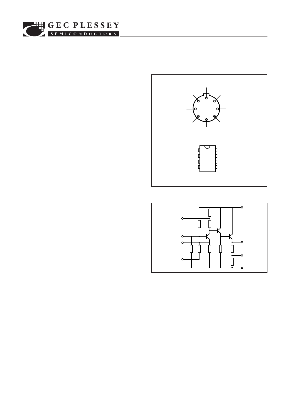
Fig.1 Pin connections
GAIN SET 5
10k
INPUT
(COMMON EMITTER
CONFIGURATION)
INPUT
(COMMON BASE
CONFIGURATION)
INPUT
(50 APPLICATIONS)
6
7
8
Fig.2 SL560C circuit diagram
ORDERING INFORMATION
SL560 C CM
SL560 C DP
5962-90520 (SMD)
DS3297 - 2.1
GROUND
2
OUTPUT CURRENT SET
OUTPUT
8
INPUT 50 OHMS APPLICATIONS
7
INPUT COMMON BASE
6
INPUT COMMON EMITTER
GAIN SET
5
4 Vcc
560
240
TR1
TR3TR2
3 OUTPUT
5003010k 1k 200
2
2k
1 GROUND
SL560
CM8
DP8
OUTPUT CURRENT
SET

SL560
SUPPLY DECOUPLING
CAPACITOR
+V
CC
GROUND
O/P
6
75
4
SUBVIS/BNC
8
13
2
LINK
SOCKET
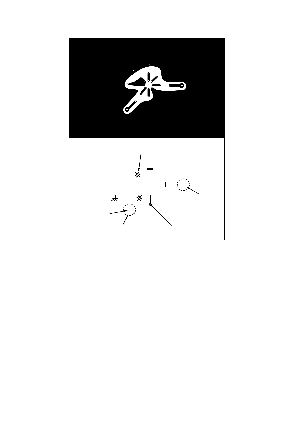
Fig.3 PC layout for 50Ω line driver (see Fig.6)
I/P
 Loading...