

GEC Plessey Semiconductors NJ8820MA, NJ8820BA Datasheet

THIS DOCUMENT IS FOR MAINTENANCE
PURPOSES ONLY AND IS NOT
RECOMMENDED FOR NEW DESIGNS
NJ8820
ABSOLUTE MAXIMUM RATINGS
Supply voltage, VDD2V
SS
Input voltage
Open drain outputs, pins 3 and 13
All other pins
Storage temperature
Storage temperature
20·5V to 7V
7V
V
SS
20·3V to VDD10·3V
265°C to 1150°C
(DG package, NJ8820MA)
255°C to 1125°C
(DP and MP packages, NJ8820)
PROGRAM
ENABLE (PE)
OSC IN
OSC OUT
D0
D1
D2
D3
F
IN
V
DD
V
SS
LATCH 1 LATCH 2 LATCH 3
‘M’ COUNTER
(10 BITS)
CONTROL LOGIC
LATCH 4 LATCH 5
‘A’ COUNTER
(7 BITS)
FREQUENCY/
PHASE
DETECTOR
V
SS
PDA
PDB
LOCK DETECT (LD)
MODULUS
CONTROL
OUTPUT (MC)
RB CH
15 16 17
f
v
REFERENCE COUNTER
(11BITS)
LATCH 6 LATCH 7 LATCH 8
42
SAMPLE/HOLD
PHASE
DETECTOR
f
r
PULSE
DETECT
SEQUENCE
COUNTER
DS0 DS1 DS2
14
7
8
9
10
11
12
4
6
5
TO
INTERNAL
LATCHES
MEMORY ENABLE
(ME)
DATA SELECT
OUTPUTS
19 2013
1
2
3
18
DATA
INPUTS
NJ8820
FREQUENCY SYNTHESISER (PROM INTERFACE)
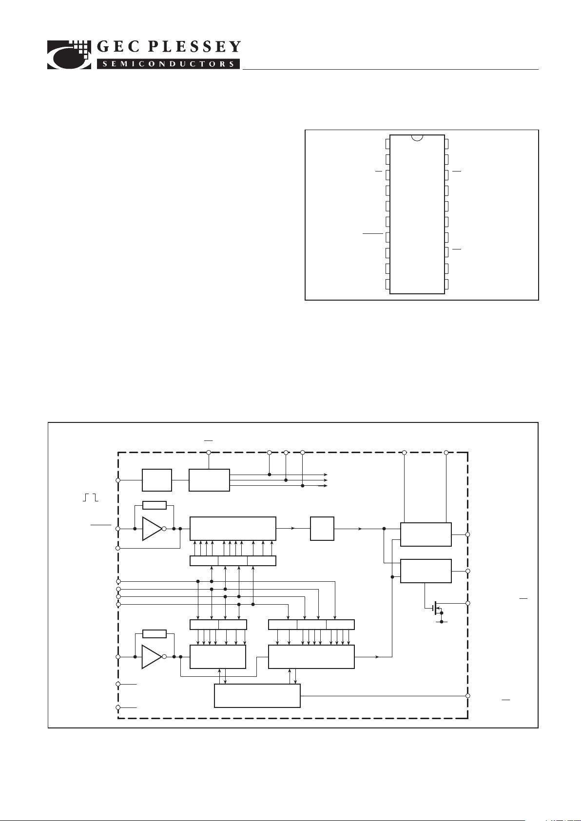
Fig.1 Pin connections - top view
T
he NJ8820 is a synthesiser circuit fabricated on the GPS
CMOS process and is capable of achieving high sideband
attenuation and low noise performance. It contains a reference
oscillator, 11-bit programmable reference divider, digital and
sample-and-hold comparators, 10-bit programmable ‘M’ counter,
7-bit programmable ‘A’ counter and the necessary control and
latch circuitry for accepting and latching the input data.
Data is presented as eight 4-bit words read from an external
memory, with the necessary timing signals generated internally.
It is intended to be used in conjunction with a two-modulus
prescaler such as the SP8710 series to produce a universal
binary coded synthesiser.
The NJ8820 is available in Plastic DIL (DP) and Miniature
Plastic DIL (MP) packages, both with operating temperature
range of 230
°
C to 170°C. The NJ8820MA is available only in
Ceramic DIL package with operating temperature range of
240
°
C to 185°C.
ORDERING INFORMATION
NJ8820 BA DP Plastic DIL Package
NJ8820 BA MP Miniature Plastic DIL Package
NJ8820 MA DG Ceramic DIL Package
FEATURES
■
Low Power Consumption
■ Direct Interface to ROM or PROM
■
High Performance Sample and Hold Phase Detector
■
>10MHz Input Frequency
Fig.2 Block diagram
CH
RB
MC
DS2
DS1
DS0
PE
ME
D3
D2
PDA
PDB
LD
F
IN
V
SS
V
DD
OSC IN
OSC OUT
D0
D1
1
2
3
4
5
6
7
8
9
10
20
19
18
17
16
15
14
13
12
11
NJ8820
DS3277-1.2
DP20, MP20,
DG20
NJ8820
f
osc
, f
FIN
= 10MHz
f
osc
, f
FIN
= 1·0MHz
I
SINK
= 4mA
I
SOURCE
= 1mA
I
SINK
= 2mA
I
SOURCE
= 1mA
I
SINK
= 1mA
I
SINK
= 4mA
I
SOURCE
= 5mA
I
SINK
= 5mA
TTL compatible
See note 1
V
BIAS
= self-bias point of PE
(nominally V
DD
/2)
mA
mA
V
V
V
V
V
V
V
V
V
V
µA
V
V
V
5·5
1·5
0·4
7
0·4
0·4
0·4
7
0·4
60·1
0·75
Supply current
OUTPUT LEVELS
Memory Enable Output (
ME)
Low level
Open drain pull-up voltage
Data Select Outputs (DS0-DS2)
High level
Low level
Modulus Control Output (
MC)
High level
Low level
Lock Detect Output (
LD)
Low level
Open drain pull-up voltage
PDB Output
High level
Low level
3-state leakage current
INPUT LEVELS
Data Inputs (D0-D3)
High level
Low level
Program Enable Input (PE)
Trigger level
4·6
4·6
4·6
4·25
V
BIAS
6100mV
2
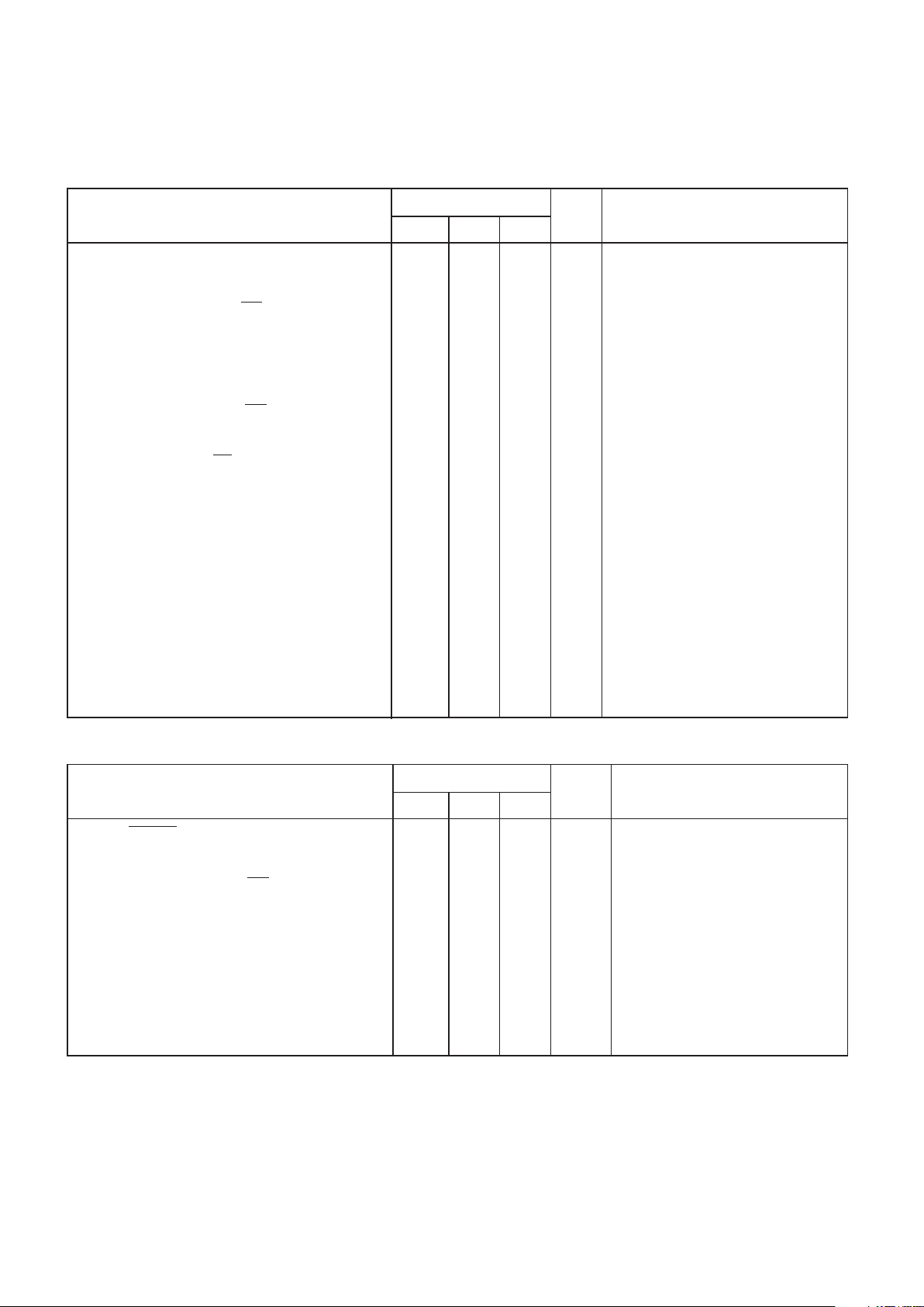
ELECTRICAL CHARACTERISTICS AT VDD = 5V
Test conditions unless otherwise stated:
V
DD–VSS
=5V ±0·5V. Temperature range NJ8820 BA: –30°C to +70°C; NJ8820 MA: –40°C to +85°C
DC Characteristics
Value
Typ. Max.
Characteristic
Min.
3·5
0·7
Units
Conditions
0 to 5V
square
wave
AC Characteristics
Value
Typ. Max.
Characteristic
Min.
Units
Conditions
mVRMS
MHz
ns
µs
µs
ns
ns
kΩ
nF
kΩ
V/Rad
µs
50
1
5
F
IN
and OSC IN input level
Max. operating frequency, f
FIN
and f
osc
Propagation delay, clock to MC
PE pulse length, t
W
Data set-up time, t
DS
Data hold time, t
DH
Digital phase detector propagation delay
Gain programming resistor, RB
Hold capacitor, CH
Output resistance, PDA
Digital phase detector gain
Power supply rise time
200
10·6
5
1
10
5
100
30
500
0·4
10MHz AC-coupled sinewave
Input squarewave V
DD
to VSS,
See note 5.
See note 2.
Pulse to V
SS
or VDD.
See note 3.
10% to 90%, see note 4.
NOTES
1. Data inputs have internal pull-up resistors to enable them to be driven from TTL outputs.
2. All counters have outputs directly synchronous with their respective clock rising edges.
3. The finite output resistance of the internal voltage follower and ‘on’ resistance of the sample switch driving this pin will add a finite time constant
to the loop. An external 1nF hold capacitor will give a maximum time constant of 5µs, typically.
4. To ensure correct operation of power-on programming.
5. Operation at up to 15MHz is possible with a full logic swing but is not guaranteed.
 Loading...