

Page 1

VAT2000 AC Drive Series
U2KV23PI0
Parallel Inter f ac e
INSTRUCTION MANUAL
GE Power Controls
NOTICE
1. Read both this manual and VAT2000 Instruction
Manual (PCST-3251) before using the
U2KV23PI0, and store in a safe place for
reference.
2. Observe the warnings, cautions and other matters
described in this manual.
3. Make sure that this manual is delivered to the final
user.
GE Power Controls
PCST-3303E-R0
Page 2

Contents
1. Specifications and Co nfiguration....................................................................... 1
2. Installation Into Inverter ...................................................................................... 2
3. Parallel Data Input................................................................................................ 4
3-1. Connection and setting procedure.................................................................. 4
3-2. Data input mode selection and signal specifications....................................... 5
3-3. Signal logic and circuit format selection.......................................................... 7
4. Usage of PSO Termin al Function........................................................................8
Appendix Table 1 CN1 pin layout ............................................................................... 9
Appendix Table 2 TB1 terminal functions.................................................................. 9
Appendix Table 3 Hardware Option Function Setting ............................................ 10
Page 3
1. Specifications and Configuration
1. Specifications and Configuration
Table 1-1 U2KV23PI0 specifications
Item Specification s
Parallel input section
Frequency setting/Speed setting
resolution
Data format
Synchronization method
Data width Select from 16-bit non-multiplexed or 8-bit m ultiplexed
Circuit voltage/ c ur r ent 24VDC/5mA (toler able leakage current 0.5mA)
Interface power
Open collector outpu t section
No. of points 2 points (PSO4, 5)
Max. voltage/current 30VDC/50mA
Min. 0.01Hz (0.1rpm)
Select from a total of elev en types i nc luding
binary/BCD, 8/ 16 bits
Select from synchronous method with strobe signal or
asynchronous method with sample
24V±10%, 0.2A or higher capacit y to be provided by
the user.
Control PCB
V23-P I0 Option PCB
Parallel data
input section
Open collector
output section
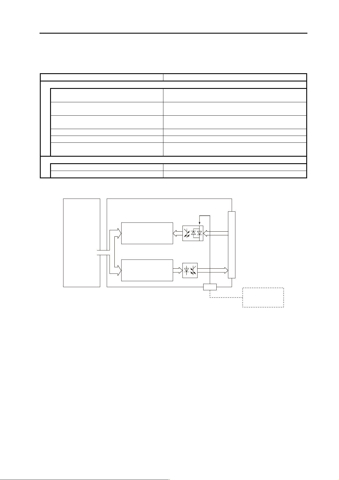
Fig. 1-1 Configuration
TB1
1
N
C
External power
supply fo r p a rallel
input
- 1 -
Page 4

2. Installation Into Inverter
2. Installation Into Inverter
The installation procedure and points of cauti on ar e as descri bed below.
(1) Remove the inverter unit' s fr ont cov er.
CAUTION
1. Wait at least 20 mi nutes after turning the power OFF bef or e star ting work. Make sure that the
displays on the operation panel have gone out before r em ovi ng the cov er.
2. After removing the cov er, confirm that the “CHARGE” LED on the unit has gone out.
Also check that the v oltage bet ween term inals L+1 or L+2 and L- is 15V or less before start ing
the inspecti ons.
(Check with the “CHA RGE” LED if t he unit is not provided with the L- terminal .)
(2) If the other option PCB is installed onto the position for option II on the control PCB cover,
install this PCB onto the position for option III.
Refer to Fig. 2-1.
2
(3) When wiring to TB1 use AWG26 to 16 (0.14 to 1.5mm
Wires should be termi nated correctly, with suitable crimp terminals or ferrules.
Pass the wires through the cable connection hole on the inver ter unit and then connect.
CAUTION
1. Observe the cauti ons li sted in Fig. 3-1 and Section 2-4 in the VAT2000 Instruction Manual
(PCST-3251) when wiring.
) for the wires.
- 2 -
Page 5

2. Installation Into Inverter
The m ou nting position
of V23-PI0
Option
Option
II
III
Option cover
Fig. 2-1 Installation of optional PCB
Control PCB cover
Option
I
NPSF - ST19 -
01
TB1
1
MEIDEN
25
26
2
N62P 30449 1 /5A MA D E IN JA PAN
SINK
CP1
1
W1
2
SOURCE
1
2
CN1
Fig. 2-2 Optional PCB
- 3 -
Page 6

3. Parallel Data Input
3. Parallel Data Input
3-1. Connection and setting procedure
(1) Connection
The parallel data input connection is shown in Fig. 3- 1.
The parallel data is i nput f r om CN1. CN1 is a DDK FRC2-C26L11-0L.
The flat cable (FRC2-A A 26- 10S ) must be provided by the user.
1. The cable length must be 30m or less.
2. The external power can be supplied from the flat cable; but if the cable length is 2m or more,
supply the power from TB 1.
The wires that can be used for TB1 are AWG26 to 16 (0.14 to 1.5mm2).
If the flat cable cannot be passed through the inv erter unit's cabl e connection hole, r emove t he
plate of the cable connec tion hole.
In this case, the protec tive structure will be IP00.
CAUTION
Parallel data
input short pin
TB1
1
2
24V power
supply
The 24V power supply is to be provided by the user
Note)
EX0
EX24
1
W1
2
CN125 1
26 2
26-core
flat cable
Sequ encer or digital sw itch
Max. 30m
Fig. 3-1 Connection of parallel data input section
(2) Se tting proced ure
1) Decide the cir c uit f ormat and data format.
2) Decide the cir c uit f ormat (open collector/open emi tt er ) with W1. (Fig. 3-5).
3) Turn ON the power, Set the parameter C02-0 to 2 (parall el fixed). (Refer t o Fig. 5-9 in the
VAT2000 Instruction M anual ( P CST- 3251) .)
4) Set the data input mode, circuit format, and parall el data format in C32-0 to C32-2.
Set the A05-2 setting v alue to 1 to cancel the hardware opti on display skip when setti ng
Note)
the C32-0 to C32-2 parameters.
(The default value is di spl ay skip.)
- 4 -
Page 7

3. Parallel Data Input
3-2. Data input mode selection and signal specifications
The following t hr ee methods can be used for the parallel input dat a input method.
1) 16-bit with strobe
2) 8-bit multi plex ed with strobe
3) 16-bit sample
These methods are select ed with parameter No. C32-0.
(1) 16-bit with strobe (C32-0 = 1)
The 16-bit data (D0 to 15) is l oaded with the rising edge of the strobe (STB).
tcy
ts th
D0~D15
OFF
STB
Inte r na l d a ta
ON
Data 0 Data 1 D ata 2
tw
Data 0 Data 1
tds
Fig. 3-2 16-bit with strobe time chart
(2) 8-bit multiplexed with strob e (C32-0 = 2)
The 16-bit data is divided into the low-order 8-bi t and high-order 8-bit wit h the LSB signal, and
each is loaded with the rising edge of the strobe (STB).
tcy
ts th
D0~D7
LSB
Data 0 (high-order) Data 1 (low-orde r) Data 2 (high-order)
OFF
ON
OFF
STB
Inte r na l d a ta
ON
tw
Data 0 Data 1
tds
Fig. 3-3 8-bit multiplexed with strobe time chart
- 5 -
Page 8

3. Parallel Data Input
(3) 16-bit sample (C32-0 = 3)
The 16-bit data is sampled every 10mS, and is loaded when the data for f our samples match.
Data 0 Data 1 Data 2 Data 3
tsp
123412
Fig. 3-4 Sample mode time chart
(4) Timing specifications
Table 3-1
Symbol Name Specifications
t cy Cycle time • 25mS
t w STB pulse width • 3mS
t s Dat a setup time • 2mS
t h Data hold time • 2mS
t ds Strobe delay 15 ~ 25mS
t da Sample mode delay 50 ~ 60mS
t sp Internal sample time 10 ± 2mS
3
412121
Data 0 Data 1
tda
Data 2 and 3 are not loaded
Note)
in this cas e.
- 6 -
Page 9

3. Parallel Data Input
3-3. Signal logic and circuit format selection
(1) Signal logic selection (D0 ~ D15)
Dn = 1 when the contact connect ed to D0 t o D15 i s ON (closed ci rcuit), or Dn = 1 when the
contact is OFF (open ci rcuit ) c an be select ed with parameter No. C32-1. (Appendix Table 3)
(2)Signal common selection (W1)
Setting of all signal c ommons to EX0 or EX24 can be selected with the W1 setting.
The sequence output m ethod open collector and open emitter can bot h be corresponded to with
this.
V23-PI0
W1
EX0
1
2
EX24
TB1-2
TB1-1
+
External
24V po wer supp ly
-
D0~D15
5 K
STB, LSB
5 K
Open collector output
Controller such as sequencer
Fig. 3-5 Short pin W1 setting
Open emitter output
- 7 -
Page 10

4. Usage of PSO Terminal Function
4. Usage of PSO Terminal Function
When using the U2KV23PI0 PSO4, 5 termi nals, set parameter C33-0, 1 sequence output signal.
(Appendix Table 3)
Refer to Table 5-4 in the VAT2000 Instruction Manual (PCST-3251) for details on the sequence
output signal functions.
Table 4-1 PSO terminal settings
Sequence output signal
Terminal Parameter No.
setting data output signal
PSO4A-PSO4B-PSO4C C33-0 5 LCL
PSO5A-PSO5B-PSO5C C33-1 6 REV
The sequence output (PSO4, 5) terminals are laid out in CN1. (Appendix Table 1)
V23-PI0
default values
PSO4
PSO5
CN1-21
CN1 -22, 23
CN1-24
CN1-25,26
Load
max. 50mA
Fig. 4-1 PSO terminal connection
max. 30V
- 8 -
Page 11

Appendix Table
Appendi x Table 1 CN1 pin la you t
Terminal No.
Symbol
CN1 - 1 D0
< Low significant bit >
Function
- 2 D1
- 3 D2
- 4 D3
- 5 D4
- 6 D5
- 7 D6
- 8 D7
- 9 D8
- 10 D9
Parallel data
CN1 - 11 D10
- 12 D11
- 13 D12
- 14 D13
- 15 D14
- 16 D15
- 17 LSB
- 18 ST B
- 19 EX24
- 20 EX0
< Most significant bit >
Indicates l ow-order 8- bit when ON. (Use for 8-bit time
multiplexed mode)
Loaded at the strobe ON to OFF edge. ( Use f or strobe
mode)
External 24V power supply i nput for the parallel dat a
input
External 24V power supply i nput common for the
parallel dat a input
CN1 - 21 PSO4 PSO4 output termi nal ( open c ollector)
- 22 COM1
- 23 COM1
PSO output terminal common
- 24 PSO5 PSO5 out put t erminal (open collector)
- 25 COM1
- 26 COM1
PSO output terminal common
25
26 2
CN1
1
View from connector insertion side
1
Appendix Table 2 TB1 ter m i na l fun c t io ns
Terminal No.
TB1 - 1 EX24
- 2 EX0
Symbol
External 24V power supply i nput for the parallel dat a
input
External 24V power supply i nput common for the
parallel dat a input
Function
- 9 -
Page 12

Appendix Table
Appendix Table 3 Hardware Option Function Setting
Block-C parameters (Basic function constants) list
No. Parameter Unit Default Min. Max. Function
C02 – Various setting input selection
=1: Analog fixed
Speed setting input
0
points selection
Traverse center
1
frequency input
points selection
T orque setting
2
input points
selection
Torque ratio 1
3
setting input points
selection
Torque bias 1
4
setting input points
selection
Torque ratio 2
5
setting input points
selection
Drive/regenerative
6
torque limit input
points selection
ASR response
7
input points
selection
Machine time
8
const ant in pu t
points selection
4. 1. 4.
2. 1. 3.
3. 1. 4.
2. 1. 3.
3. 1. 4.
2. 1. 3.
3. 1. 3.
2. 1. 3.
2. 1. 3.
=2: Serial/parallel fixed
=3: Panel fixe d
=4: Sequence
=1: Analog fixed
=2: Panel fixe d
=3: Sequence
=1: Analog fixed
=2: Serial fixed
=3: Panel fixe d
=4: Sequence
=1: Serial fixed
=2: Panel fixe d
=3: Sequence
=1: Analog fixed
=2: Serial fixed
=3: Panel fixe d
=4: Sequence
=1: Serial fixed
=2: Panel fixe d
=3: Sequence
=1: Analog fixed
=2: Serial fixed
=3: Sequence
=1: Serial fixed
=2: Panel fixe d
=3: Sequence
=1: Serial fixed
=2: Panel fixe d
=3: Sequence
Application
ST V/f VEC PM
O
O
OO
OO
OO
OO
OO
OO
OO
Block-C parameters (H/W option function constants) list
No. Parameter Unit Default Min. Max. Function
C32 – PC (parallel) Interface
Input mode
0
(strobe)
Input mode (input
1
logic)
2 Data format 1. 0. 10.
Setting data Format Setting resolution Setting range
0
1
2
3
4
5
6
7
8
9
10
Hz = Frequency setting [ For V/f control (Constant torque, reduced torque) (C30-0 = 1, 2) ]
rpm: Speed setting
Set this when th e P ar all el in terfac e opti on (U 2K V 2 3PL 0) h as b een mou nt ed .
16-bit binary
16-bit binary
16-bit binary
16-bit binary
16-bit BCD
16-bit BCD
16-bit BCD
16-bit BCD
8-bit binary
12-bit binary
16-bit binary
1. 1. 3.
1. 1. 2.
0.01Hz/LSB (0.1rpm/LSB)
0.1Hz/LSB ( 1rpm/LSB)
0.01%LSB
0.1%LSB
0.01Hz/LSB (0.1rpm/LSB)
0.1Hz/LSB ( 1rpm/LSB)
0.01%LSB
0.1%LSB
1/255%
1/4095%
1/65535%
For IM speed sensorless vector control (C30-0 = 3)
For IM speed vector control (C30-0 = 4)
For PM motor c ontrol (C30- 0 = 5)
=1: 16 -bit strobe
=2: 8 -bit time multiplexed strobe
=3: 16 -bit sample
=1: 1 at closed circuit
=2: 1 at opened circ u it
Set accord in g to th e f oll owi ng
table.
0 to 440.00Hz (0.0 to 6553.5rpm or Nmax)
440.0Hz (0 to Nmax rpm)
100.00%
100.0%
99.99Hz (0.0 to 999.9rpm)
100.0Hz (0 to Nmax rpm)
99.99%
100.0%
100.0%
100.0%
100.0%
Application
ST V/f VEC PM
O
O
O
- 10 -
Page 13

Appendix Table
Block-C parameters (H/W option function constants) list
No. Parameter Unit Default Min. Max. Function
C33 – Sequence output terminal function (Option)
PSO4 Output
0
parameters
PSO5 Output
1
parameters
5. 0. 24. O
6. 0. 24.
Set this when th e r el ay in t erface
option (U2KV23RY0) and Parallel
interface option (U2KV23PI0) are
mounted.
Refer to Instruction Manual
(PCST-3301) for other details.
Application
ST V/f VEC PM
O
Value Output
signal
0 RUN 8 ATN 16 ACC 24 ULMT
1 FLT 9 SPD1 17 DCC
2 MC 10 SPD2 18 AUXDV
3 RDY1 11 COP 19 ALM
4RDY2 12EC0 20FAN
5 LCL 13 EC1 21 ASW
6 REV 14 EC2 22 ZSP
7 IDET 15 EC3 23 LLMT
Value Output
signal
Value Output
signal
Value Output
signal
- 11 -
 Loading...