

Page 1
GE Energy Connections
Grid Solutions
MiCOM P40 Agile
P54A, P54B, P54C, P54E
Technical Manual
Single Br
eaker Multi-End Current Differential IED (Non Distance)
Hardware Version: M,P
Software Version: 01
Publication Reference: P54xMED-TM-EN-1
Page 2

Page 3

Contents
Chapter 1 Introduction 1
1 Chapter Overview 3
2 Foreword 4
2.1 Target Audience 4
2.2 Typographical Conventions 4
2.3 Nomenclature 5
2.4 Compliance 5
3 Product Scope 6
3.1 Ordering Options 6
4 Features and Functions 7
4.1 Current Differential Protection Functions 7
4.2 Protection Functions 7
4.3 Control Functions 7
4.4 Measurement Functions 8
4.5 Communication Functions 8
5 Logic Diagrams 9
6 Functional Overview 11
Chapter 2 Safety Information 13
1 Chapter Overview 15
2 Health and Safety 16
3 Symbols 17
4 Installation, Commissioning and Servicing 18
4.1 Lifting Hazards 18
4.2 Electrical Hazards 18
4.3 UL/CSA/CUL Requirements 19
4.4 Fusing Requirements 19
4.5 Equipment Connections 20
4.6 Protection Class 1 Equipment Requirements 20
4.7 Pre-energisation Checklist 21
4.8 Peripheral Circuitry 21
4.9 Upgrading/Servicing 22
5 Decommissioning and Disposal 23
6 Regulatory Compliance 24
6.1 EMC Compliance: 2014/30/EU 24
6.2 LVD Compliance: 2014/35/EU 24
6.3 R&TTE Compliance: 2014/53/EU 24
6.4 UL/CUL Compliance 24
6.5 ATEX Compliance: 2014/34/EU 24
Chapter 3 Hardware Design 27
1 Chapter Overview 29
2 Hardware Architecture 30
2.1 Coprocessor Hardware Architecture 30
3 Mechanical Implementation 32
3.1 Housing Variants 32
3.2 List of Boards 33
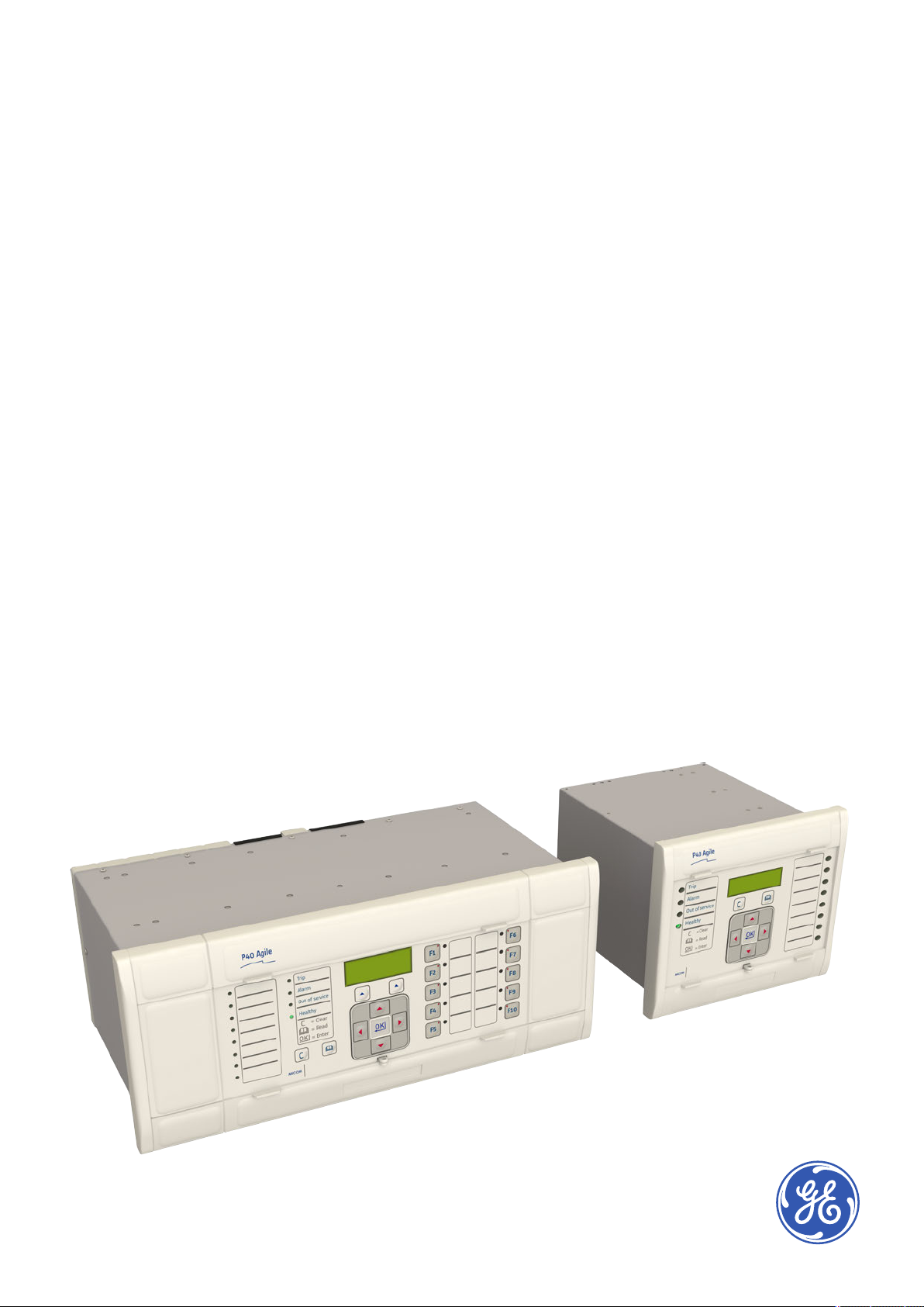
4 Front Panel 35
4.1 Front Panel 35
4.1.1 Front Panel Compartments 35
4.1.2 Keypad 36
Page 4

Contents P54A/B/C/E
4.1.3 Front Serial Port (SK1) 36
4.1.4 Front Parallel Port (SK2) 37
4.1.5 Fixed Function LEDs 37
4.1.6 Function Keys 37
4.1.7 Programable LEDs 38
5 Rear Panel 39
6 Boards and Modules 41
6.1 PCBs 41
6.2 Subassemblies 41
6.3 Main Processor Board 42
6.4 Power Supply Board 43
6.4.1 Watchdog 45
6.4.2 Rear Serial Port 46
6.5 Input Module - 1 Transformer Board 47
6.5.1 Input Module Circuit Description 48
6.5.2 Transformer Board 49
6.5.3 Input Board 50
6.6 Standard Output Relay Board 51
6.7 IRIG-B Board 52
6.8 Fibre Optic Board 53
6.9 Rear Communication Board 54
6.10 Ethernet Board 54
6.11 Redundant Ethernet Board 56
6.12 Coprocessor Board 58
6.12.1 Current Differential Inputs 58
6.12.2 Coprocessor board with 1PPS input 58
Chapter 4 Software Design 61
1 Chapter Overview 63
2 Sofware Design Overview 64
3 System Level Software 65
3.1 Real Time Operating System 65
3.2 System Services Software 65
3.3 Self-Diagnostic Software 65
3.4 Startup Self-Testing 65
3.4.1 System Boot 65
3.4.2 System Level Software Initialisation 66
3.4.3 Platform Software Initialisation and Monitoring 66
3.5 Continuous Self-Testing 66
4 Platform Software 68
4.1 Record Logging 68
4.2 Settings Database 68
4.3 Interfaces 68
5 Protection and Control Functions 69
5.1 Acquisition of Samples 69
5.2 Frequency Tracking 69
5.3 Direct Use of Sample Values 69
5.4 System Level Software Initialisation 69
5.5 Fourier Signal Processing 70
5.6 Programmable Scheme Logic 71
5.7 Event Recording 71
5.8 Disturbance Recorder 72
5.9 Fault Locator 72
5.10 Function Key Interface 72
Chapter 5 Configuration 73
ii P54xMED-TM-EN-1
Page 5

P54A/B/C/E Contents
1 Chapter Overview 75
2 Settings Application Software 76
3 Using the HMI Panel 77
3.1 Navigating the HMI Panel 78
3.2 Getting Started 78
3.3 Default Display 79
3.4 Default Display Navigation 80
3.5 Password Entry 81
3.6 Processing Alarms and Records 81
3.7 Menu Structure 82
3.8 Changing the Settings 83
3.9 Direct Access (The Hotkey menu) 84
3.9.1 Setting Group Selection Using Hotkeys 84
3.9.2 Control Inputs 84
3.9.3 Circuit Breaker Control 85
3.10 Function Keys 85
4 Line Parameters 87
4.1 Tripping Mode 87
4.1.1 CB Trip Conversion Logic Diagram 87
4.2 Residual Compensation 88
4.3 Mutual Compensation 88
5 Date and Time Configuration 90
5.1 Using an SNTP Signal 90
5.2 Using an IRIG-B Signal 90
5.3 Using an IEEE 1588 PTP Signal 90
5.4 Without a Timing Source Signal 91
5.5 Time Zone Compensation 91
5.6 Daylight Saving Time Compensation 92
6 Settings Group Selection 93
Chapter 6 Current Differential Protection 95
1 Chapter Overview 97
2 Current Differential Protection Principle 98
2.1 Numerical Current Differential Protection 98
2.2 Multi-ended Line Differential Protection 99
2.3 Basic Principles and Algorithm Design for Multi-ended Differential Protection 99
2.3.1 Fault Discrimination 99
2.3.2 Differential Characteristics 100
2.3.3 Basic Algorithm 102
2.3.4 Features of Multi-Ended Line Differential 102
2.3.5 Algorithm Overview 102
2.3.6 Communication Requirements 103
3 Charging Current Compensation 104
4 Synchronisation of Current Signals 106
4.1 Time Alignment using Ping-Pong Technique 106
4.2 Remote Terminal Time Alignment 107
4.3 Time Delay Interpolation 108
5 CT Saturation 109
6 CT Compensation 112
7 Current Differential Intertripping 113
8 Stub Bus Differential Protection 114
9 Application Notes 115
9.1 Multi-End Current Differential Protection 115
9.2 Feeder Topology 116
9.3 Configuring the Feeder Topology 116
9.4 Line Parameter Data 117
P54xMED-TM-EN-1 iii
Page 6

Contents P54A/B/C/E
9.5 Configuring the Protection Communications 118
9.6 Setting Up the Phase Differential Characteristic 119
9.7 Sensitivity Under Heavy Loads 119
9.8 Permissive Intertripping 121
9.9 CT Ratio Correction Setting Guidelines 121
9.10 Feeders with Small Tapped Loads 122
Chapter 7 Autoreclose 123
1 Chapter Overview 125
2 Introduction to Autoreclose 126
3 Autoreclose Implementation 127
3.1 Autoreclose Logic Inputs from External Sources 128
3.1.1 Circuit Breaker Healthy Input 128
3.1.2 Inhibit Autoreclose Input 128
3.1.3 Block Autoreclose Input 128
3.1.4 Reset Lockout Input 129
3.1.5 Pole Discrepancy Input 129
3.1.6 External Trip Indication 129
3.2 Autoreclose Logic Inputs 129
3.2.1 Trip Initiation Signals 129
3.2.2 Circuit Breaker Status Inputs 129
3.2.3 System Check Signals 129
3.3 Autoreclose Logic Outputs 129
3.4 Autoreclose Operating Sequence 130
3.4.1 AR Timing Sequence - Transient Fault 130
3.4.2 AR Timing Sequence - Evolving/Permanent Fault 130
3.4.3 AR Timing Sequence - Evolving/Permanent Fault Single-phase 131
4 Autoreclose System Map 132
4.1 Autoreclose System Map Diagrams 134
4.2 Autoreclose Internal Signals 139
4.3 Autoreclose DDB Signals 141
5 Logic Modules 147
5.1 Circuit Breaker Status Monitor 147
5.1.1 CB State Monitor Logic diagram 148
5.2 Circuit Breaker Open Logic 149
5.2.1 Circuit Breaker Open Logic Diagram 149
5.3 Circuit Breaker in Service Logic 149
5.3.1 Circuit Breaker in Service Logic Diagram 149
5.3.2 Autoreclose OK Logic Diagram 150
5.4 Autoreclose Enable 150
5.4.1 Autoreclose Enable Logic Diagram 150
5.5 Autoreclose Modes 150
5.5.1 Single-Phase and Three-Phase Autoreclose 151
5.5.2 Autoreclose Modes Enable Logic Diagram 152
5.6 AR Force Three-Phase Trip Logic 152
5.6.1 AR Force Three-Phase Trip Logic Diagram 152
5.7 Autoreclose Initiation Logic 152
5.7.1 Autoreclose Initiation Logic Diagram 154
5.7.2 Autoreclose Trip Test Logic Diagram 154
5.7.3 AR External Trip Initiation Logic Diagram 155
5.7.4 Protection Reoperation and Evolving Fault Logic Diagram 156
5.7.5 Fault Memory Logic Diagram 156
5.8 Autoreclose In Progress 156
5.8.1 Autoreclose In Progress Logic Diagram 157
5.9 Sequence Counter 157
5.9.1 Autoreclose Sequence Counter Logic Diagram 158
5.10 Autoreclose Cycle Selection 158
iv P54xMED-TM-EN-1
Page 7

P54A/B/C/E Contents
5.10.1 Single-Phase Autoreclose Cycle Selection Logic Diagram 158
5.10.2 3-phase Autoreclose Cycle Selection 159
5.11 Dead Time Control 159
5.11.1 Dead Time Start Enable Logic Diagram 160
5.11.2 1-phase Dead Time Logic Diagram 161
5.11.3 3-phase Dead Time Logic Diagram 162
5.12 Circuit Breaker Autoclose 162
5.12.1 Circuit Breaker Autoclose Logic Diagram 163
5.13 Reclaim Time 163
5.13.1 Prepare Reclaim Initiation Logic Diagram 164
5.13.2 Reclaim Time Logic Diagram 164
5.13.3 Succesful Autoreclose Signals Logic Diagram 165
5.13.4 Autoreclose Reset Successful Indication Logic Diagram 165
5.14 CB Healthy and System Check Timers 165
5.14.1 CB Healthy and System Check Timers Logic Diagram 166
5.15 Autoreclose Shot Counters 166
5.15.1 Autoreclose Shot Counters Logic Diagram 167
5.16 Circuit Breaker Control 168
5.16.1 CB Control Logic Diagram 168
5.17 Circuit Breaker Trip Time Monitoring 169
5.17.1 CB Trip Time Monitoring Logic Diagram 169
5.18 Autoreclose Lockout 169
5.18.1 CB Lockout Logic Diagram 170
5.19 Reset Circuit Breaker Lockout 171
5.19.1 Reset CB Lockout Logic Diagram 171
5.20 Pole Discrepancy 172
5.20.1 Pole Discrepancy Logic Diagram 172
5.21 Circuit Breaker Trip Conversion 172
5.21.1 CB Trip Conversion Logic Diagram 173
5.22 Monitor Checks for CB Closure 173
5.22.1 Check Synchronisation Monitor for CB Closure 174
5.22.2 Voltage Monitor for CB Closure 175
5.23 Synchronisation Checks for CB Closure 175
5.23.1 Three-phase Autoreclose System Check Logic Diagram 177
5.23.2 CB Manual Close System Check Logic Diagram 178
6 Setting Guidelines 179
6.1 De-ionising Time Guidance 179
6.2 Dead Timer Setting Guidelines 179
6.2.1 Example Dead Time Calculation 179
6.3 Reclaim Time Setting Guidelines 180
Chapter 8 CB Fail Protection 181
1 Chapter Overview 183
2 Circuit Breaker Fail Protection 184
3 Circuit Breaker Fail Implementation 185
3.1 Circuit Breaker Fail Timers 185
3.2 Zero Crossing Detection 185
4 Circuit Breaker Fail Logic 187
4.1 Circuit Breaker Fail Logic - Part 1 187
4.2 Circuit Breaker Fail Logic - Part 2 188
4.3 Circuit Breaker Fail Logic - Part 3 189
4.4 Circuit Breaker Fail Logic - Part 4 190
5 Application Notes 191
5.1 Reset Mechanisms for CB Fail Timers 191
5.2 Setting Guidelines (CB fail Timer) 191
5.3 Setting Guidelines (Undercurrent) 192
P54xMED-TM-EN-1 v
Page 8

Contents P54A/B/C/E
Chapter 9 Current Protection Functions 193
1 Chapter Overview 195
2 Phase Fault Overcurrent Protection 196
2.1 POC Implementation 196
2.2 Directional Element 196
2.3 POC Logic 198
3 Negative Sequence Overcurrent Protection 199
3.1 Negative Sequence Overcurrent Protection Implementation 199
3.2 Directional Element 199
3.3 NPSOC Logic 200
3.4 Application Notes 200
3.4.1 Setting Guidelines (Current Threshold) 200
3.4.2 Setting Guidelines (Time Delay) 200
3.4.3 Setting Guidelines (Directional element) 201
4 Earth Fault Protection 202
4.1 Earth Fault Protection Implementation 202
4.2 IDG Curve 202
4.3 Directional Element 203
4.3.1 Residual Voltage Polarisation 203
4.3.2 Negative Sequence Polarisation 204
4.4 Earth Fault Protection Logic 205
4.5 Application Notes 205
4.5.1 Residual Voltage Polarisation Setting Guidelines 205
4.5.2 Setting Guidelines (Directional Element) 205
5 Sensitive Earth Fault Protection 207
5.1 SEF Protection Implementation 207
5.2 EPATR B Curve 207
5.3 Sensitive Earth Fault Protection Logic 208
5.4 Application Notes 209
5.4.1 Insulated Systems 209
5.4.2 Setting Guidelines (Insulated Systems) 210
6 High Impedance REF 212
6.1 High Impedance REF Principle 212
7 Thermal Overload Protection 214
7.1 Single Time Constant Characteristic 214
7.2 Dual Time Constant Characteristic 214
7.3 Thermal Overload Protection Implementation 215
7.4 Thermal Overload Protection Logic 215
7.5 Application Notes 215
7.5.1 Setting Guidelines for Dual Time Constant Characteristic 215
7.5.2 Setting Guidelines for Single Time Constant Characteristic 217
8 Broken Conductor Protection 219
8.1 Broken Conductor Protection Implementation 219
8.2 Broken Conductor Protection Logic 219
8.3 Application Notes 219
8.3.1 Setting Guidelines 219
Chapter 10 Voltage Protection Functions 221
1 Chapter Overview 223
2 Undervoltage Protection 224
2.1 Undervoltage Protection Implementation 224
2.2 Undervoltage Protection Logic 225
2.3 Application Notes 226
2.3.1 Undervoltage Setting Guidelines 226
3 Overvoltage Protection 227
vi P54xMED-TM-EN-1
Page 9

P54A/B/C/E Contents
3.1 Overvoltage Protection Implementation 227
3.2 Overvoltage Protection Logic 228
3.3 Application Notes 229
3.3.1 Overvoltage Setting Guidelines 229
4 Compensated Overvoltage 230
5 Residual Overvoltage Protection 231
5.1 Residual Overvoltage Protection Implementation 231
5.2 Residual Overvoltage Logic 232
5.3 Application Notes 232
5.3.1 Calculation for Solidly Earthed Systems 232
5.3.2 Calculation for Impedance Earthed Systems 233
5.3.3 Setting Guidelines 234
Chapter 11 Frequency Protection Functions 235
1 Chapter Overview 237
2 Frequency Protection 238
2.1 Underfrequency Protection 238
2.1.1 Underfrequency Protection Implementation 238
2.1.2 Underfrequency Protection logic 239
2.1.3 Application Notes 239
2.2 Overfrequency Protection 239
2.2.1 Overfrequency Protection Implementation 239
2.2.2 Overfrequency Protection logic 240
2.2.3 Application Notes 240
3 Independent R.O.C.O.F Protection 241
3.1 Indepenent R.O.C.O.F Protection Implementation 241
3.2 Independent R.O.C.O.F Protection Logic 241
Chapter 12 Monitoring and Control 243
1 Chapter Overview 245
2 Event Records 246
2.1 Event Types 246
2.1.1 Opto-input Events 247
2.1.2 Contact Events 247
2.1.3 Alarm Events 247
2.1.4 Fault Record Events 248
2.1.5 Maintenance Events 248
2.1.6 Protection Events 248
2.1.7 Security Events 249
2.1.8 Platform Events 249
3 Disturbance Recorder 250
4 Measurements 251
4.1 Measured Quantities 251
4.2 Measurement Setup 251
4.3 Fault Locator 251
4.4 Opto-input Time Stamping 251
5 CB Condition Monitoring 252
5.1 Broken Current Accumulator 253
5.2 CB Trip Counter 253
5.3 CB Operating Time Accumulator 254
5.4 Excessive Fault Frequency Counter 254
5.5 Reset Lockout Alarm 255
5.6 CB Condition Monitoring Logic 256
5.7 Reset Circuit Breaker Lockout 256
5.7.1 Reset CB Lockout Logic Diagram 257
5.8 Application Notes 257
P54xMED-TM-EN-1 vii
Page 10

Contents P54A/B/C/E
5.8.1 Setting the Thresholds for the Total Broken Current 257
5.8.2 Setting the thresholds for the Number of Operations 258
5.8.3 Setting the thresholds for the Operating Time 258
5.8.4 Setting the Thresholds for Excesssive Fault Frequency 258
6 CB State Monitoring 259
6.1 CB State Monitor Logic diagram 260
7 Circuit Breaker Control 261
7.1 CB Control using the IED Menu 261
7.2 CB Control using the Hotkeys 262
7.3 CB Control using the Function Keys 262
7.4 CB Control using the Opto-inputs 263
7.5 Remote CB Control 263
7.6 CB Healthy Check 264
7.7 Synchronisation Check 264
7.8 CB Control AR Implications 264
7.9 CB Control Logic Diagram 265
8 Pole Dead Function 266
8.1 Pole Dead Logic 266
9 System Checks 267
9.1 System Checks Implementation 267
9.1.1 VT Connections 267
9.1.2 Voltage Monitoring 268
9.1.3 Check Synchronisation 268
9.1.4 Check Syncronisation Vector Diagram 268
9.2 Voltage Monitor for CB Closure 270
9.3 Check Synchronisation Monitor for CB Closure 271
9.4 System Check PSL 272
9.5 Application Notes 272
9.5.1 Predictive Closure of Circuit Breaker 272
9.5.2 Voltage and Phase Angle Correction 272
Chapter 13 Supervision 275
1 Chapter Overview 277
2 Current Differential Supervision 278
2.1 Current Differential Starter Supervision 278
2.1.1 Current Differential Starter Supervision Logic 280
2.1.2 Current Differential Start Logic 281
2.2 Switched Communication Path Supervision 281
2.3 Communications Asymmetry Supervision 282
3 Voltage Transformer Supervision 284
3.1 Loss of One or Two Phase Voltages 284
3.2 Loss of all Three Phase Voltages 284
3.3 Absence of all Three Phase Voltages on Line Energisation 284
3.4 VTS Implementation 285
3.5 VTS Logic 286
4 Current Transformer Supervision 289
4.1 Differential CTS 289
4.2 Differential CTS Logic 290
4.3 CTS Implementation 290
4.4 Standard CTS Logic 291
4.5 CTS Blocking 291
4.6 Application Notes 291
4.6.1 Setting Guidelines 291
4.6.2 Differential CTS Setting Guidelines 292
5 Trip Circuit Supervision 293
5.1 Trip Circuit Supervision Scheme 1 293
viii P54xMED-TM-EN-1
Page 11

P54A/B/C/E Contents
5.1.1 Resistor Values 293
5.1.2 PSL for TCS Scheme 1 294
5.2 Trip Circuit Supervision Scheme 2 294
5.2.1 Resistor Values 295
5.2.2 PSL for TCS Scheme 2 295
5.3 Trip Circuit Supervision Scheme 3 295
5.3.1 Resistor Values 296
5.3.2 PSL for TCS Scheme 3 296
Chapter 14 Digital I/O and PSL Configuration 297
1 Chapter Overview 299
2 Configuring Digital Inputs and Outputs 300
3 Scheme Logic 301
3.1 PSL Editor 302
3.2 PSL Schemes 302
3.3 PSL Scheme Version Control 302
4 Configuring the Opto-Inputs 303
5 Assigning the Output Relays 304
6 Fixed Function LEDs 305
6.1 Trip LED Logic 305
7 Configuring Programmable LEDs 306
8 Function Keys 308
9 Control Inputs 309
Chapter 15 Fibre Teleprotection 311
1 Chapter Overview 313
2 Fibre Teleprotection Implementation 314
2.1 Communication Setup 314
2.2 Protection Communications Channel 315
2.3 1.1.1.Protection Comms Message Slot Allocation for Each Protection Scheme 315
2.4 Error Handling for Protection Communications 319
2.5 Fibre Teleprotection Scheme Terminal Addressing 320
2.6 Physical Connection 320
2.6.1 Direct Connection 321
2.6.2 Indirect Connection 321
3 Communications Supervision 322
4 IM64 Logic 323
5 Application Notes 325
5.1 Scheme Reconfiguration 325
5.2 Alarm Management 325
5.3 Alarm Logic 325
5.4 Two-ended Scheme Extended Supervision 326
5.5 Three-ended Scheme Extended Supervision 327
Chapter 16 Electrical Teleprotection 329
1 Chapter Overview 331
2 Introduction 332
3 Teleprotection Scheme Principles 333
3.1 Direct Tripping 333
3.2 Permissive Tripping 333
4 Implementation 334
5 Configuration 335
6 Connecting to Electrical InterMiCOM 337
6.1 Short Distance 337
P54xMED-TM-EN-1 ix
Page 12

Contents P54A/B/C/E
6.2 Long Distance 337
7 Application Notes 338
Chapter 17 Communications 341
1 Chapter Overview 343
2 Communication Interfaces 344
3 Serial Communication 345
3.1 EIA(RS)232 Bus 345
3.2 EIA(RS)485 Bus 345
3.2.1 EIA(RS)485 Biasing Requirements 346
3.3 K-Bus 346
4 Standard Ethernet Communication 348
4.1 Hot-Standby Ethernet Failover 348
5 Redundant Ethernet Communication 349
5.1 Supported Protocols 349
5.2 Parallel Redundancy Protocol 350
5.3 High-Availability Seamless Redundancy (HSR) 351
5.3.1 HSR Multicast Topology 351
5.3.2 HSR Unicast Topology 352
5.3.3 HSR Application in the Substation 352
5.4 Rapid Spanning Tree Protocol 353
5.5 Self Healing Protocol 354
5.6 Dual Homing Protocol 355
5.7 Configuring IP Addresses 357
5.7.1 Configuring the IED IP Address 358
5.7.2 Configuring the REB IP Address 358
5.8 PRP/HSR Configurator 361
5.8.1 Connecting the IED to a PC 361
5.8.2 Installing the Configurator 362
5.8.3 Starting the Configurator 362
5.8.4 PRP/HSR Device Identification 363
5.8.5 Selecting the Device Mode 363
5.8.6 PRP/HSR IP Address Configuration 363
5.8.7 SNTP IP Address Configuration 363
5.8.8 Check for Connected Equipment 363
5.8.9 PRP Configuration 363
5.8.10 HSR Configuration 364
5.8.11 Filtering Database 364
5.8.12 End of Session 365
5.9 RSTP Configurator 365
5.9.1 Connecting the IED to a PC 365
5.9.2 Installing the Configurator 366
5.9.3 Starting the Configurator 366
5.9.4 RSTP Device Identification 366
5.9.5 RSTP IP Address Configuration 367
5.9.6 SNTP IP Address Configuration 367
5.9.7 Check for Connected Equipment 367
5.9.8 RSTP Configuration 367
5.9.9 End of Session 368
5.10 Switch Manager 368
5.10.1 Installation 369
5.10.2 Setup 370
5.10.3 Network Setup 370
5.10.4 Bandwidth Used 370
5.10.5 Reset Counters 370
5.10.6 Check for Connected Equipment 370
5.10.7 Mirroring Function 371
x P54xMED-TM-EN-1
Page 13

P54A/B/C/E Contents
5.10.8 Ports On/Off 371
5.10.9 VLAN 371
5.10.10 End of Session 371
6 Simple Network Management Protocol (SNMP) 372
6.1 SNMP Management Information Bases 372
6.2 Main Processor MIBS Structure 372
6.3 Redundant Ethernet Board MIB Structure 373
6.4 Accessing the MIB 377
6.5 Main Processor SNMP Configuration 377
7 Data Protocols 379
7.1 Courier 379
7.1.1 Physical Connection and Link Layer 379
7.1.2 Courier Database 380
7.1.3 Settings Categories 380
7.1.4 Setting Changes 380
7.1.5 Event Extraction 380
7.1.6 Disturbance Record Extraction 382
7.1.7 Programmable Scheme Logic Settings 382
7.1.8 Time Synchronisation 382
7.1.9 Courier Configuration 383
7.2 IEC 60870-5-103 384
7.2.1 Physical Connection and Link Layer 384
7.2.2 Initialisation 385
7.2.3 Time Synchronisation 385
7.2.4 Spontaneous Events 385
7.2.5 General Interrogation (GI) 385
7.2.6 Cyclic Measurements 385
7.2.7 Commands 385
7.2.8 Test Mode 386
7.2.9 Disturbance Records 386
7.2.10 Command/Monitor Blocking 386
7.2.11 IEC 60870-5-103 Configuration 386
7.3 DNP 3.0 387
7.3.1 Physical Connection and Link Layer 388
7.3.2 Object 1 Binary Inputs 388
7.3.3 Object 10 Binary Outputs 388
7.3.4 Object 20 Binary Counters 389
7.3.5 Object 30 Analogue Input 389
7.3.6 Object 40 Analogue Output 390
7.3.7 Object 50 Time Synchronisation 390
7.3.8 DNP3 Device Profile 390
7.3.9 DNP3 Configuration 398
7.4 IEC 61850 399
7.4.1 Benefits of IEC 61850 400
7.4.2 IEC 61850 Interoperability 400
7.4.3 The IEC 61850 Data Model 400
7.4.4 IEC 61850 in MiCOM IEDs 401
7.4.5 IEC 61850 Data Model Implementation 402
7.4.6 IEC 61850 Communication Services Implementation 402
7.4.7 IEC 61850 Peer-to-peer (GOOSE) communications 402
7.4.8 Mapping GOOSE Messages to Virtual Inputs 402
7.4.9 Ethernet Functionality 403
7.4.10 IEC 61850 Configuration 403
7.4.11 IEC 61850 Edition 2 404
8 Read Only Mode 408
8.1 IEC 60870-5-103 Protocol Blocking 408
8.2 Courier Protocol Blocking 408
8.3 IEC 61850 Protocol Blocking 409
8.4 Read-Only Settings 409
P54xMED-TM-EN-1 xi
Page 14

Contents P54A/B/C/E
8.5 Read-Only DDB Signals 409
9 Time Synchronisation 410
9.1 Demodulated IRIG-B 410
9.1.1 IRIG-B Implementation 411
9.2 SNTP 411
9.2.1 Loss of SNTP Server Signal Alarm 411
9.3 IEEE 1588 Precision time Protocol 411
9.3.1 Accuracy and Delay Calculation 411
9.3.2 PTP Domains 412
9.4 Time Synchronsiation using the Communication Protocols 412
Chapter 18 Cyber-Security 413
1 Overview 415
2 The Need for Cyber-Security 416
3 Standards 417
3.1 NERC Compliance 417
3.1.1 CIP 002 418
3.1.2 CIP 003 418
3.1.3 CIP 004 418
3.1.4 CIP 005 418
3.1.5 CIP 006 418
3.1.6 CIP 007 419
3.1.7 CIP 008 419
3.1.8 CIP 009 419
3.2 IEEE 1686-2007 419
4 Cyber-Security Implementation 421
4.1 NERC-Compliant Display 421
4.2 Four-level Access 422
4.2.1 Blank Passwords 423
4.2.2 Password Rules 423
4.2.3 Access Level DDBs 424
4.3 Enhanced Password Security 424
4.3.1 Password Strengthening 424
4.3.2 Password Validation 424
4.3.3 Password Blocking 425
4.4 Password Recovery 426
4.4.1 Password Recovery 426
4.4.2 Password Encryption 427
4.5 Disabling Physical Ports 427
4.6 Disabling Logical Ports 427
4.7 Security Events Management 428
4.8 Logging Out 430
Chapter 19 Installation 431
1 Chapter Overview 433
2 Handling the Goods 434
2.1 Receipt of the Goods 434
2.2 Unpacking the Goods 434
2.3 Storing the Goods 434
2.4 Dismantling the Goods 434
3 Mounting the Device 435
3.1 Flush Panel Mounting 435
3.2 Rack Mounting 436
4 Cables and Connectors 438
4.1 Terminal Blocks 438
4.2 Power Supply Connections 439
xii P54xMED-TM-EN-1
Page 15

P54A/B/C/E Contents
4.3 Earth Connnection 439
4.4 Current Transformers 439
4.5 Voltage Transformer Connections 440
4.6 Watchdog Connections 440
4.7 EIA(RS)485 and K-Bus Connections 440
4.8 IRIG-B Connection 440
4.9 Opto-input Connections 440
4.10 Output Relay Connections 440
4.11 Ethernet Metallic Connections 441
4.12 Ethernet Fibre Connections 441
4.13 RS232 connection 441
4.14 Download/Monitor Port 441
4.15 GPS Fibre Connection 441
4.16 Fibre Communication Connections 441
5 Case Dimensions 442
5.1 Case Dimensions 40TE 442
5.2 Case Dimensions 60TE 443
5.3 Case Dimensions 80TE 444
Chapter 20 Commissioning Instructions 445
1 Chapter Overview 447
2 General Guidelines 448
3 Commissioning Test Menu 449
3.1 Opto I/P Status Cell (Opto-input Status) 449
3.2 Relay O/P Status Cell (Relay Output Status) 449
3.3 Test Port Status Cell 449
3.4 Monitor Bit 1 to 8 Cells 449
3.5 Test Mode Cell 450
3.6 Test Pattern Cell 450
3.7 Contact Test Cell 450
3.8 Test LEDs Cell 450
3.9 Test Autoreclose Cell 450
3.10 Static Test Mode 451
3.11 Loopback Mode 451
3.12 IM64 Test Pattern 452
3.13 IM64 Test Mode 452
3.14 Red and Green LED Status Cells 452
3.15 Using a Monitor Port Test Box 452
4 Commissioning Equipment 453
4.1 Recommended Commissioning Equipment 453
4.2 Essential Commissioning Equipment 453
4.3 Advisory Test Equipment 454
5 Product Checks 455
5.1 Product Checks with the IED De-energised 455
5.1.1 Visual Inspection 456
5.1.2 Current Transformer Shorting Contacts 456
5.1.3 Insulation 456
5.1.4 External Wiring 456
5.1.5 Watchdog Contacts 457
5.1.6 Power Supply 457
5.2 Product Checks with the IED Energised 457
5.2.1 Watchdog Contacts 457
5.2.2 Test LCD 458
5.2.3 Date and Time 458
5.2.4 Test LEDs 459
5.2.5 Test Alarm and Out-of-Service LEDs 459
P54xMED-TM-EN-1 xiii
Page 16

Contents P54A/B/C/E
5.2.6 Test Trip LED 459
5.2.7 Test User-programmable LEDs 459
5.2.8 Test Opto-inputs 459
5.2.9 Test Output Relays 459
5.2.10 Test Serial Communication Port RP1 460
5.2.11 Test Serial Communication Port RP2 461
5.2.12 Test Ethernet Communication 462
5.3 Secondary Injection Tests 462
5.3.1 Test Current Inputs 462
5.3.2 Test Voltage Inputs 462
6 Electrical Intermicom Communication Loopback 464
6.1 Setting up the Loopback 464
6.2 Loopback Test 464
6.2.1 InterMicom Command Bits 465
6.2.2 InterMicom Channel Diagnostics 465
6.2.3 Simulating a Channel Failure 465
7 Intermicom 64 Communication 466
7.1 Checking the Interface 466
7.2 Setting up the Loopback 466
7.3 Loopback Test 467
8 Setting Checks 468
8.1 Apply Application-specific Settings 468
8.1.1 Transferring Settings from a Settings File 468
8.1.2 Entering settings using the HMI 468
9 IEC 61850 Edition 2 Testing 470
9.1 Using IEC 61850 Edition 2 Test Modes 470
9.1.1 IED Test Mode Behaviour 470
9.1.2 Sampled Value Test Mode Behaviour 470
9.2 Simulated Input Behaviour 471
9.3 Testing Examples 471
9.3.1 Test Procedure for Real Values 472
9.3.2 Test Procedure for Simulated Values - No Plant 472
9.3.3 Test Procedure for Simulated Values - With Plant 473
9.3.4 Contact Test 474
10 Current Differential Protection 475
10.1 Current Differential Bias Characteristic 475
10.1.1 Lower Slope 475
10.1.2 Upper Slope 476
10.2 Current Differential Operation and Contact Assignment 476
11 Protection Timing Checks 478
11.1 Dependency Conditions 478
11.2 Overcurrent Check 478
11.3 Connecting the Test Circuit 478
11.4 Performing the Test 479
11.5 Check the Operating Time 479
12 System Check and Check Synchronism 480
12.1 Check Synchronism Pass 480
12.2 Check Synchronism Fail 480
13 Check Trip and Autoreclose Cycle 481
14 End-to-End Communication Tests 482
14.1 Remove Local Loopbacks 482
14.1.1 Restoring Direct Fibre Connections 482
14.1.2 Restoring C37.94 Fibre Connections 483
14.2 Remove Remote Loopbacks 483
14.3 Verify Communication between IEDs 483
15 Onload Checks 484
15.1 Confirm Voltage Connections 484
15.2 Confirm Current Connections 484
xiv P54xMED-TM-EN-1
Page 17

P54A/B/C/E Contents
15.3 Measure Capacitive Charging Current 485
15.4 Check Differential Current 485
15.5 Check Current Transformer Polarity 485
15.6 On-load Directional Test 485
16 Final Checks 486
Chapter 21 Maintenance and Troubleshooting 487
1 Chapter Overview 489
2 Maintenance 490
2.1 Maintenance Checks 490
2.1.1 Alarms 490
2.1.2 Opto-isolators 490
2.1.3 Output Relays 490
2.1.4 Measurement Accuracy 490
2.2 Replacing the Device 491
2.3 Repairing the Device 492
2.4 Removing the front panel 492
2.5 Replacing PCBs 493
2.5.1 Replacing the main processor board 493
2.5.2 Replacement of communications boards 494
2.5.3 Replacement of the input module 495
2.5.4 Replacement of the power supply board 495
2.5.5 Replacement of the I/O boards 496
2.6 Recalibration 496
2.7 Changing the battery 496
2.7.1 Post Modification Tests 497
2.7.2 Battery Disposal 497
2.8 Cleaning 497
3 Troubleshooting 498
3.1 Self-Diagnostic Software 498
3.2 Power-up Errors 498
3.3 Error Message or Code on Power-up 498
3.4 Out of Service LED on at power-up 499
3.5 Error Code during Operation 500
3.5.1 Backup Battery 500
3.6 Mal-operation during testing 500
3.6.1 Failure of Output Contacts 500
3.6.2 Failure of Opto-inputs 500
3.6.3 Incorrect Analogue Signals 501
3.7 Coprocessor board failures 501
3.7.1 Signalling failure alarm (on its own) 501
3.7.2 C diff failure alarm (on its own) 501
3.7.3 Signalling failure and C diff failure alarms together 501
3.7.4 Incompatible IED 501
3.7.5 Comms changed 501
3.7.6 IEEE C37.94 fail 502
3.8 PSL Editor Troubleshooting 502
3.8.1 Diagram Reconstruction 502
3.8.2 PSL Version Check 502
3.9 Repair and Modification Procedure 502
Chapter 22 Technical Specifications 505
1 Chapter Overview 507
2 Interfaces 508
2.1 Front Serial Port 508
2.2 Download/Monitor Port 508
P54xMED-TM-EN-1 xv
Page 18

Contents P54A/B/C/E
2.3 Rear Serial Port 1 508
2.4 Fibre Rear Serial Port 1 508
2.5 Rear Serial Port 2 509
2.6 Optional Rear Serial Port (SK5) 509
2.7 IRIG-B (Demodulated) 509
2.8 IRIG-B (Modulated) 509
2.9 Rear Ethernet Port Copper 510
2.10 Rear Ethernet Port Fibre 510
2.10.1 100 Base FX Receiver Characteristics 510
2.10.2 100 Base FX Transmitter Characteristics 511
2.11 1 PPS Port 511
2.12 Fibre Teleprotection Interface 511
3 Protection Functions 512
3.1 Phase Current Differential Protection 512
3.2 Fibre Teleprotection Transfer Times 512
3.3 Autoreclose and Check Synychronism 512
3.4 Phase Overcurrent Protection 512
3.4.1 Phase Overcurrent Directional Parameters 513
3.5 Earth Fault Protection 513
3.5.1 Earth Fault Directional Parameters 513
3.6 Sensitive Earth Fault Protection 514
3.6.1 Sensitive Earth Fault Protection Directional Element 514
3.7 High Impedance Restricted Earth Fault Protection 514
3.8 Negative Sequence Overcurrent Protection 515
3.8.1 NPSOC Directional Parameters 515
3.9 Circuit Breaker Fail and Undercurrent Protection 515
3.10 Broken Conductor Protection 515
3.11 Thermal Overload Protection 515
4 Monitoring, Control and Supervision 516
4.1 Voltage Transformer Supervision 516
4.2 Standard Current Transformer Supervision 516
4.3 Differential Current Transformer Supervision 516
4.4 CB State and Condition Monitoring 516
4.5 PSL Timers 517
5 Measurements and Recording 518
5.1 General 518
5.2 Disturbance Records 518
5.3 Event, Fault and Maintenance Records 518
5.4 Fault Locator 518
6 Ratings 519
6.1 AC Measuring Inputs 519
6.2 Current Transformer Inputs 519
6.3 Voltage Transformer Inputs 519
6.4 Auxiliary Supply Voltage 519
6.5 Nominal Burden 520
6.6 Power Supply Interruption 520
6.7 Battery Backup 521
7 Input / Output Connections 522
7.1 Isolated Digital Inputs 522
7.1.1 Nominal Pickup and Reset Thresholds 522
7.2 Standard Output Contacts 522
7.3 High Break Output Contacts 523
7.4 Watchdog Contacts 523
8 Mechanical Specifications 524
8.1 Physical Parameters 524
8.2 Enclosure Protection 524
8.3 Mechanical Robustness 524
xvi P54xMED-TM-EN-1
Page 19

P54A/B/C/E Contents
8.4 Transit Packaging Performance 524
9 Type Tests 525
9.1 Insulation 525
9.2 Creepage Distances and Clearances 525
9.3 High Voltage (Dielectric) Withstand 525
9.4 Impulse Voltage Withstand Test 525
10 Environmental Conditions 526
10.1 Ambient Temperature Range 526
10.2 Temperature Endurance Test 526
10.3 Ambient Humidity Range 526
10.4 Corrosive Environments 526
11 Electromagnetic Compatibility 527
11.1 1 MHz Burst High Frequency Disturbance Test 527
11.2 Damped Oscillatory Test 527
11.3 Immunity to Electrostatic Discharge 527
11.4 Electrical Fast Transient or Burst Requirements 527
11.5 Surge Withstand Capability 527
11.6 Surge Immunity Test 528
11.7 Immunity to Radiated Electromagnetic Energy 528
11.8 Radiated Immunity from Digital Communications 528
11.9 Radiated Immunity from Digital Radio Telephones 528
11.10 Immunity to Conducted Disturbances Induced by Radio Frequency Fields 528
11.11 Magnetic Field Immunity 529
11.12 Conducted Emissions 529
11.13 Radiated Emissions 529
11.14 Power Frequency 529
12 Regulatory Compliance 530
12.1 EMC Compliance: 2014/30/EU 530
12.2 LVD Compliance: 2014/35/EU 530
12.3 R&TTE Compliance: 2014/53/EU 530
12.4 UL/CUL Compliance 530
12.5 ATEX Compliance: 2014/34/EU 530
Appendix A Ordering Options 533
Appendix B Settings and Signals 535
Appendix C Wiring Diagrams 537
P54xMED-TM-EN-1 xvii
Page 20

Contents P54A/B/C/E
xviii P54xMED-TM-EN-1
Page 21

Table of Figures
Figure 1: Key to logic diagrams 10
Figure 2: Functional Overview 11
Figure 3: Hardware architecture 30
Figure 4: Coprocessor hardware architecture 31
Figure 5: Exploded view of IED 32
Figure 6: Front panel (60TE) 35
Figure 7: Rear view of populated case 39
Figure 8: Terminal block types 40
Figure 9: Rear connection to terminal block 41
Figure 10: Main processor board 42
Figure 11: Power supply board 43
Figure 12: Power supply assembly 44
Figure 13: Power supply terminals 45
Figure 14: Watchdog contact terminals 46
Figure 15: Rear serial port terminals 47
Figure 16: Input module - 1 transformer board 47
Figure 17: Input module schematic 48
Figure 18: Transformer board 49
Figure 19: Input board 50
Figure 20: Standard output relay board - 8 contacts 51
Figure 21: IRIG-B board 52
Figure 22: Fibre optic board 53
Figure 23: Rear communication board 54
Figure 24: Ethernet board 54
Figure 25: Redundant Ethernet board 56
Figure 26: Fully populated Coprocessor board 58
Figure 27: Software Architecture 64
Figure 28: Frequency Response (indicative only) 71
Figure 29: Navigating the HMI 78
Figure 30: Default display navigation 80
Figure 31: Circuit Breaker Trip Conversion Logic Diagram (Module 63) 87
Figure 32: Sample multi-ended system 100
Figure 33: Current differential discriminative criterion 101
Figure 34: Overall scheme designed for multi-ended differential protection 103
Figure 35: Two-ended transmission line 104
Figure 36: Ping-pong measurement for alignment of current signals 106
Figure 37: Snapshot of available data for processing at each terminal 108
Figure 38: CT saturation technique 109
Page 22

Table of Figures P54A/B/C/E
Figure 39: Original current waveforms 110
Figure 40: Ipos and Ineg current waveforms 111
Figure 41: Internal external fault binary 111
Figure 42: CT Compensation 112
Figure 43: Permissive Intertripping example 113
Figure 44: Stub Bus protection 114
Figure 45: Six terminal, four junction topology and ring structure 115
Figure 46: Six terminal ring structure with channel allocation 115
Figure 47: Six terminal, four junction topology 116
Figure 48: Autoreclose sequence for a Transient Fault 130
Figure 49: Autoreclose sequence for an evolving or permanent fault 131
Figure 50: Autoreclose sequence for an evolving or permanent fault - single-phase operation 131
Figure 51: Key to logic diagrams 133
Figure 52: Autoreclose System Map - part 1 134
Figure 53: Autoreclose System Map - part 2 135
Figure 54: Autoreclose System Map - part 3 136
Figure 55: Autoreclose System Map - part 4 137
Figure 56: Autoreclose System Map - part 5 138
Figure 57: CB State Monitor logic diagram (Module 1) 148
Figure 58: Circuit Breaker Open logic diagram (Module 3) 149
Figure 59: CB In Service logic diagram (Module 4) 149
Figure 60: Autoreclose OK logic diagram (Module 8) 150
Figure 61: Autoreclose Enable logic diagram (Module 5) 150
Figure 62: Autoreclose Modes Enable logic diagram (Module 9) 152
Figure 63: Force Three-phase Trip logic diagram (Module 10) 152
Figure 64: Autoreclose Initiation logic diagram (Module 11) 154
Figure 65: Autoreclose Trip Test logic diagram (Module 12) 154
Figure 66: Autoreclose initiation by external trip or evolving conditions (Module 13) 155
Figure 67: Protection Reoperation and Evolving Fault logic diagram (Module 20) 156
Figure 68: Fault Memory logic diagram (Module 15) 156
Figure 69: Autoreclose In Progress logic diagram (Module 16) 157
Figure 70: Autoreclose Sequence Counter logic diagram (Module 18) 158
Figure 71: Single-phase Autoreclose Cycle Selection logic diagram (Module 19) 158
Figure 72: Three-phase Autoreclose Cycle Selection logic diagram (Module 21) 159
Figure 73: Dead time Start Enable logic diagram (Module 22) 160
Figure 74: Single-phase Dead Time logic diagram (Module 24) 161
Figure 75: Three-phase Dead Time logic diagram (Module 25) 162
Figure 76: Circuit Breaker Autoclose Logic Diagram (Module 32) 163
Figure 77: Prepare Reclaim Initiation Logic Diagram (Module 34) 164
Figure 78: Reclaim Time logic diagram (Module 35) 164
xx P54xMED-TM-EN-1
Page 23

P54A/B/C/E Table of Figures
Figure 79: Successful Autoreclose Signals logic diagram (Module 36) 165
Figure 80: Autoreclose Reset Successful Indication logic diagram (Module 37) 165
Figure 81: Circuit Breaker Healthy and System Check Timers Healthy logic diagram (Module 39) 166
Figure 82: Autoreclose Shot Counters logic diagram (Module 41) 167
Figure 83: CB Control logic diagram (Module 43) 168
Figure 84: Circuit Breaker Trip Time Monitoring logic diagram (Module 53) 169
Figure 85: AR Lockout Logic Diagram (Module 55) 170
Figure 86: Reset Circuit Breaker Lockout Logic Diagram (Module 57) 171
Figure 87: Pole Discrepancy Logic Diagram (Module 62) 172
Figure 88: Circuit Breaker Trip Conversion Logic Diagram (Module 63) 173
Figure 89: Check Synchronisation Monitor for CB closure (Module 60) 174
Figure 90: Voltage Monitor for CB Closure (Module 59) 175
Figure 91: Three-phase Autoreclose System Check Logic Diagram (Module 45) 177
Figure 92: CB Manual Close System Check Logic Diagram (Module 51) 178
Figure 93: Circuit Breaker Fail logic - part 1 187
Figure 94: Circuit Breaker Fail logic - part 2 188
Figure 95: Circuit Breaker Fail logic - part 3 189
Figure 96: Circuit Breaker Fail logic - part 4 190
Figure 97: CB Fail timing 192
Figure 98: Phase Overcurrent Protection logic diagram 198
Figure 99: Negative Phase Sequence Overcurrent Protection logic diagram 200
Figure 100: IDG Characteristic 203
Figure 101: Earth Fault Protection logic diagram 205
Figure 102: EPATR B characteristic shown for TMS = 1.0 208
Figure 103: Sensitive Earth Fault Protection logic diagram 208
Figure 104: Current distribution in an insulated system with C phase fault 209
Figure 105: Phasor diagrams for insulated system with C phase fault 210
Figure 106: Positioning of core balance current transformers 211
Figure 107: High Impedance REF principle 212
Figure 108: High Impedance REF Connection 213
Figure 109: Thermal overload protection logic diagram 215
Figure 110: Spreadsheet calculation for dual time constant thermal characteristic 216
Figure 111: Dual time constant thermal characteristic 216
Figure 112: Broken conductor logic 219
Figure 113: Undervoltage - single and three phase tripping mode (single stage) 225
Figure 114: Overvoltage - single and three phase tripping mode (single stage) 228
Figure 115: Residual Overvoltage logic 232
Figure 116: Residual voltage for a solidly earthed system 233
Figure 117: Residual voltage for an impedance earthed system 234
Figure 118: Underfrequency logic (single stage) 239
P54xMED-TM-EN-1 xxi
Page 24

Table of Figures P54A/B/C/E
Figure 119: Overfrequency logic (single stage) 240
Figure 120: Rate of change of frequency logic (single stage) 241
Figure 121: Fault recorder stop conditions 248
Figure 122: Broken Current Accumulator logic diagram 253
Figure 123: CB Trip Counter logic diagram 253
Figure 124: Operating Time Accumulator 254
Figure 125: Excessive Fault Frequency logic diagram 254
Figure 126: Reset Lockout Alarm logic diagram 255
Figure 127: CB Condition Monitoring logic diagram 256
Figure 128: Reset Circuit Breaker Lockout Logic Diagram (Module 57) 257
Figure 129: CB State Monitor logic diagram (Module 1) 260
Figure 130: Hotkey menu navigation 262
Figure 131: Default function key PSL 263
Figure 132: Remote Control of Circuit Breaker 264
Figure 133: CB Control logic diagram (Module 43) 265
Figure 134: Pole Dead logic 266
Figure 135: Check Synchronisation vector diagram 269
Figure 136: Voltage Monitor for CB Closure (Module 59) 270
Figure 137: Check Synchronisation Monitor for CB closure (Module 60) 271
Figure 138: System Check PSL 272
Figure 139: Current Differential Starter Supervision Logic 280
Figure 140: Current Differential function Start logic 281
Figure 141: Switched Communication Path supervision 282
Figure 142: Communication Asymmetry Supervision 283
Figure 143: VTS logic 288
Figure 144: Differential CTS 290
Figure 145: Standard CTS 291
Figure 146: TCS Scheme 1 293
Figure 147: PSL for TCS Scheme 1 294
Figure 148: TCS Scheme 2 295
Figure 149: PSL for TCS Scheme 2 295
Figure 150: TCS Scheme 3 296
Figure 151: PSL for TCS Scheme 3 296
Figure 152: Scheme Logic Interfaces 301
Figure 153: Trip LED logic 305
Figure 154: Fibre teleprotection connections for a six-terminal scheme 315
Figure 155: Two terminal single channel scheme 315
Figure 156: Two terminal dual channel scheme 316
Figure 157: Three terminal scheme 316
Figure 158: Four terminal scheme 317
xxii P54xMED-TM-EN-1
Page 25

P54A/B/C/E Table of Figures
Figure 159: Five terminal scheme 318
Figure 160: Six terminal scheme 319
Figure 161: IM64 channel fail and scheme fail logic 323
Figure 162: IM64 general alarm signals logic 323
Figure 163: IM64 communications mode and IEEE C37.94 alarm signals 324
Figure 164: IM64 two-terminal scheme extended supervision 327
Figure 165: IM64 three-terminal scheme extended supervision 327
Figure 166: Example assignment of InterMiCOM signals within the PSL 336
Figure 167: Direct connection 337
Figure 168: Indirect connection using modems 337
Figure 169: RS485 biasing circuit 346
Figure 170: Remote communication using K-Bus 347
Figure 171: IED attached to separate LANs 350
Figure 172: HSR multicast topology 351
Figure 173: HSR unicast topology 352
Figure 174: HSR application in the substation 353
Figure 175: IED attached to redundant Ethernet star or ring circuit 353
Figure 176: IED, bay computer and Ethernet switch with self healing ring facilities 354
Figure 177: Redundant Ethernet ring architecture with IED, bay computer and Ethernet switches 354
Figure 178: Redundant Ethernet ring architecture with IED, bay computer and Ethernet switches
after failur
e
355
Figure 179: Dual homing mechanism 356
Figure 180: Application of Dual Homing Star at substation level 357
Figure 181: IED and REB IP address configuration 358
Figure 182: Connection using (a) an Ethernet switch and (b) a media converter 362
Figure 183: Connection using (a) an Ethernet switch and (b) a media converter 366
Figure 184: Control input behaviour 389
Figure 185: Data model layers in IEC61850 401
Figure 186: Edition 2 system - backward compatibility 405
Figure 187: Edition 1 system - forward compatibility issues 405
Figure 188: Example of Standby IED 406
Figure 189: Standby IED Activation Process 407
Figure 190: GPS Satellite timing signal 410
Figure 191: Timing error using ring or line topology 412
Figure 192: Default display navigation 422
Figure 193: Location of battery isolation strip 435
Figure 194: Rack mounting of products 436
Figure 195: Terminal block types 438
Figure 196: 40TE case dimensions 442
Figure 197: 60TE case dimensions 443
P54xMED-TM-EN-1 xxiii
Page 26

Table of Figures P54A/B/C/E
Figure 198: 80TE case dimensions 444
Figure 199: RP1 physical connection 460
Figure 200: Remote communication using K-bus 461
Figure 201: InterMicom loopback testing 464
Figure 202: Simulated input behaviour 471
Figure 203: Test example 1 472
Figure 204: Test example 2 473
Figure 205: Test example 3 474
Figure 206: Current Differential Bias Characteristics 475
Figure 207: Possible terminal block types 492
Figure 208: Front panel assembly 494
xxiv P54xMED-TM-EN-1
Page 27

CHAPTER 1
INTRODUCTION
Page 28

Chapter 1 - Introduction P54A/B/C/E
2 P54xMED-TM-EN-1
Page 29

P54A/B/C/E Chapter 1 - Introduction
1 CHAPTER OVERVIEW
This chapter provides some general information about the technical manual and an introduction to the device(s)
described in this technical manual.
This chapter contains the following sections:
Chapter Overview 3
eword 4
For
Product Scope 6
Features and Functions 7
Logic Diagrams 9
Functional Overview 11
P54xMED-TM-EN-1 3
Page 30

Chapter 1 - Introduction P54A/B/C/E
2 FOREWORD
This technical manual provides a functional and technical description of General Electric's P54A, P54B, P54C, P54E,
ell as a comprehensive set of instructions for using the device. The level at which this manual is written
as w
assumes that you are already familiar with protection engineering and have experience in this discipline. The
description of principles and theory is limited to that which is necessary to understand the product. For further
details on general protection engineering theory, we refer you to Alstom's publication NPAG, which is available
online or from our contact centre.
We have attempted to make this manual as accurate, comprehensive and user-friendly as possible. However we
cannot guarantee that it is free from errors. Nor can we state that it cannot be improved. We would therefore be
very pleased to hear from you if you discover any errors, or have any suggestions for improvement. Our policy is to
provide the information necessary to help you safely specify, engineer, install, commission, maintain, and
eventually dispose of this product. We consider that this manual provides the necessary information, but if you
consider that more details are needed, please contact us.
All feedback should be sent to our contact centre via the following URL:
www.gegridsolutions.com/contact
2.1 TARGET AUDIENCE
This manual is aimed towards all professionals charged with installing, commissioning, maintaining,
tr
oubleshooting, or operating any of the products within the specified product range. This includes installation and
commissioning personnel as well as engineers who will be responsible for operating the product.
The level at which this manual is written assumes that installation and commissioning engineers have knowledge
of handling electronic equipment. Also, system and protection engineers have a thorough knowledge of protection
systems and associated equipment.
2.2 TYPOGRAPHICAL CONVENTIONS
The following typographical conventions are used throughout this manual.
● The names for special k
For example: ENTER
● When describing software applications, menu items, buttons, labels etc as they appear on the screen are
written in bold type.
For example: Select Save from the file menu.
● Filenames and paths use the courier font
For example: Example\File.text
● Special terminology is written with leading capitals
For example: Sensitive Earth Fault
● If reference is made to the IED's internal settings and signals database, the menu group heading (column)
text is written in upper case italics
For example: The SYSTEM DATA column
● If reference is made to the IED's internal settings and signals database, the setting cells and DDB signals are
written in bold italics
For example: The Language cell in the SYSTEM DATA column
● If reference is made to the IED's internal settings and signals database, the value of a cell's content is
written in the Courier font
For example: The Language cell in the SYSTEM DATA column contains the value English
eys appear in capital letters.
4 P54xMED-TM-EN-1
Page 31

P54A/B/C/E Chapter 1 - Introduction
2.3 NOMENCLATURE
Due to the technical nature of this manual, many special terms, abbreviations and acronyms are used throughout
the manual. Some of these terms ar
specific terms used by General Electric. The first instance of any acronym or term used in a particular chapter is
explained. In addition, a separate glossary is available on the General Electric website, or from the General Electric
contact centre.
We would like to highlight the following changes of nomenclature however:
● The word 'relay' is no longer used to describe the device itself. Instead, the device is referred to as the 'IED'
(Intelligent Electronic Device), the 'device', or the 'product'. The word 'relay' is used purely to describe the
electromechanical components within the device, i.e. the output relays.
● British English is used throughout this manual.
● The British term 'Earth' is used in favour of the American term 'Ground'.
e well-known industry-specific terms while others may be special product-
2.4 COMPLIANCE
The device has undergone a range of extensive testing and certification processes to ensure and prove
compatibility with all tar
Specifications chapter.
get markets. A detailed description of these criteria can be found in the Technical
P54xMED-TM-EN-1 5
Page 32

Chapter 1 - Introduction P54A/B/C/E
3 PRODUCT SCOPE
The P54A, P54B, P54C and P54E IEDs provide high-speed, multi-ended differential protection (without the need of
GPS synchr
applications. They also include 4-shot phase-segregated Autoreclose protection for single circuit breaker
applications.
The algorithms of these devices work differently from their standard counterparts. The device samples at double
the speed and does not use Fourier transformation to calculate phasors. It uses sampled values directly, which
enables subcycle tripping.
The P54C and P54E provide more I/O and are housed in a larger cases than the P54A and P54B. The differences
between the model variants are summarised in the table below:
Number of CT Inputs 4 5 5 5 5 5 5
Number of VT inputs 4 4 4 4 4 4
Opto-coupled digital inputs 8 8 16 16 24 24 32
Standard relay output contacts 8 8 16 8 16 32 32
High speed high break output contacts 4 8
Key functions for each product are described below:
onisation) for electrical feeders having between 2 and 6 terminals, for both overhead line and cable
Feature/Variant P54A P54B P54C P54E
● P54A compact (40TE), economical line differ
ential protection without VT inputs, offering non-directional
backup protection.
● P54B compact (40TE), economical line differential protection with directionalised back-up protection and
inbuilt reclosing and check synchronism.
● P54C transmission-class 1/3-pole tripping line differential protection with backup protection and inbuilt
reclosing and check synchronism (built from today’s P543 hardware).
● P54E transmission-class 1/3-pole tripping line differential protection with back-up protection and inbuilt
reclosing and check synchronism with a large number of binary I/O for traditional hardwired schemes (built
from P545 hardware).
Multi-ended line differential relays are not compatible with the conventional line differential MiCOM Agile relays.
3.1 ORDERING OPTIONS
All current models and variants for this product are defined in an interactive spreadsheet called the CORTEC. This is
av
ailable on the company website.
Alternatively, you can obtain it via the Contact Centre at the following URL:
www.gegridsolutions.com/contact
A copy of the CORTEC is also supplied as a static table in the Appendices of this document. However, it should only
be used for guidance as it provides a snapshot of the interactive data taken at the time of publication.
6 P54xMED-TM-EN-1
Page 33

P54A/B/C/E Chapter 1 - Introduction
4 FEATURES AND FUNCTIONS
4.1 CURRENT DIFFERENTIAL PROTECTION FUNCTIONS
Feature IEC 61850 ANSI
Phase segregated current differential protection DifPDIF1 87L
Between 2 and 6 terminal lines/cables
Self-synchronization feature
InterMiCOM64 telepr
communication (optional)
otection for direct device-to-device
4.2 PROTECTION FUNCTIONS
Feature IEC 61850 ANSI
Tripping Mode (1 & 3 pole) PTRC
ABC and ACB phase rotation
Phase overcurrent , with optional directionality (4 stages) OcpPTOC/RDIR 50/51/67
Earth/Ground overcurrent stages, with optional directionality (4
stages)
Sensitive earth fault (SEF) (4 stages) SenPTOC/RDIR 50N/51N/67N
High impedance restricted earth fault (REF) SenRefPDIF 64
Negative sequence overcurrent stages, with optional
dir
ectionality (4 stages)
Broken conductor, used to detect open circuit faults 46
Thermal overload protection ThmPTTR 49
Undervoltage protection (2 stages) VtpPhsPTUV 27
Overvoltage protection (2 stages) VtpPhsPTOV 59
Remote overvoltage protection (2 stages) VtpCmpPTOV 59R
Residual voltage protection (2 stages) VtpResPTOV 59N
Underfrequency protection (4 stages) FrqPTUF 81
Overfrequency protection (2 stages) FrqPTOF 81
Rate of change of frequency protection (4 stages) DfpPFRC 81
High speed breaker fail suitable for re-tripping and back-
tripping (2 stages)
Current Transformer supervision 46
Voltage transformer supervision 47/27
Auto-reclose (4 shots) RREC 79
Check synchronisation (2 stages) RSYN 25
EfdPTOC/RDIR 50N/51N/ 67N
NgcPTOC/RDIR 67/46
RBRF 50BF
4.3 CONTROL FUNCTIONS
Feature IEC 61850 ANSI
Watchdog contacts
Read-only mode
Function keys FnkGGIO
P54xMED-TM-EN-1 7
Page 34

Chapter 1 - Introduction P54A/B/C/E
Feature IEC 61850 ANSI
Programmable LEDs LedGGIO
Programmable hotkeys
Programmable allocation of digital inputs and outputs
Fully customizable menu texts
Circuit breaker control, status & condition monitoring XCBR 52
CT supervision
VT supervision
Trip circuit and coil supervision
Control inputs PloGGIO1
Power-up diagnostics and continuous self-monitoring
Dual rated 1A and 5A CT inputs
Alternative setting groups (4)
Graphical programmable scheme logic (PSL)
Fault locator RFLO
4.4 MEASUREMENT FUNCTIONS
Measurement Function IEC 61850 ANSI
Measurement of all instantaneous & integrated values
(Exact range of measurements depend on the device model)
Disturbance recorder for waveform capture – specified in samples per cycle RDRE DFR
Fault Records
Maintenance Records
Event Records / Event logging Event records
Time Stamping of Opto-inputs Yes Yes
MET
4.5 COMMUNICATION FUNCTIONS
Feature ANSI
NERC compliant cyber-security
Front RS232 serial communication port for configuration 16S
Rear serial RS485 communication port for SCADA control 16S
2 Additional rear serial communication ports for SCADA control and
telepr
otection (fibre and copper) (optional)
Ethernet communication (optional) 16E
Redundant Ethernet communication (optional) 16E
Courier Protocol 16S
IEC 61850 edition 1 or edition 2 (optional) 16E
IEC 60870-5-103 (optional) 16S
DNP3.0 over serial link (optional) 16S
DNP3.0 over Ethernet (optional) 16E
SNMP 16E
IRIG-B time synchronisation (optional) CLK
IEEE 1588 PTP (Edition 2 devices only)
16S
8 P54xMED-TM-EN-1
Page 35

P54A/B/C/E Chapter 1 - Introduction
5 LOGIC DIAGRAMS
This technical manual contains many logic diagrams, which should help to explain the functionality of the device.
Although this manual has been designed to be as specific as possible to the chosen pr
diagrams, which have elements applicable to other products. If this is the case, a qualifying note will accompany
the relevant part.
The logic diagrams follow a convention for the elements used, using defined colours and shapes. A key to this
convention is provided below. We recommend viewing the logic diagrams in colour rather than in black and white.
The electronic version of the technical manual is in colour, but the printed version may not be. If you need coloured
diagrams, they can be provided on request by calling the contact centre and quoting the diagram number.
oduct, it may contain
P54xMED-TM-EN-1 9
Page 36

V00063
K
ey:
DDB Signal
I
nternal function
&AND gate
O
R gate
1
Setting cell
Setting value Timer
SR Latch
R
eset Dominant
Internal Signal
0Logic 0
Comparator for detecting
o
vervalues
Energising Quantity
Hardcoded setting
R
D
Q
S
C
omparator for detecting
undervalues
Switch
Measurement Cell
Derived setting
SR Latch
HMI key
Pulse / Latch
C
onnection / Node Inverted logic input
Soft switch
Latched on positive edge
XM
ultiplier
2
1
NOT gate
XOR
X
OR gate
R
Q
S
Internal Calculation
Switch
Bandpass filter
Chapter 1 - Introduction P54A/B/C/E
Figure 1: Key to logic diagrams
10 P54xMED-TM-EN-1
Page 37

CTS VTS50BF 79
Fault records
Disturbance
Record
Measurements
PSL
Local
Communicationcomm. port
LEDs
conventional
signalling
protection
communication
Self monitoring
85FL
50N/
51N
46BC
1 Optic
port
2
ndst
Optic
port
25
50/27
27/59
59N
87P
50/51
67
2ndRemote
comm. port
IEC
61850
X
BUS1
V
ref
V
I
Neutral current
from parallel line
(if present)
I
M
I
E sen
V
ref
64
94
67N
I/ V
67N
SEF
67/46
Remote
LINE
Remote
Optional
Always
available
P54A, P54B
P54C, P54E
E00071
P54A/B/C/E Chapter 1 - Introduction
6 FUNCTIONAL OVERVIEW
This diagram is applicable to several multi-end current differential protection products in the P40L family; P54A,
P54B, P54C and P54E. Use the diagram k
technical manual.
ey to determine the features relevant to the product described in this
Figure 2: Functional Overview
P54xMED-TM-EN-1 11
Page 38

Chapter 1 - Introduction P54A/B/C/E
12 P54xMED-TM-EN-1
Page 39

CHAPTER 2
SAFETY INFORMATION
Page 40

Chapter 2 - Safety Information P54A/B/C/E
14 P54xMED-TM-EN-1
Page 41

P54A/B/C/E Chapter 2 - Safety Information
1 CHAPTER OVERVIEW
This chapter provides information about the safe handling of the equipment. The equipment must be properly
installed and handled in or
be familiar with information contained in this chapter before unpacking, installing, commissioning, or servicing the
equipment.
This chapter contains the following sections:
Chapter Overview 15
Health and Safety 16
Symbols 17
Installation, Commissioning and Servicing 18
Decommissioning and Disposal 23
Regulatory Compliance 24
der to maintain it in a safe condition and to keep personnel safe at all times. You must
P54xMED-TM-EN-1 15
Page 42

Chapter 2 - Safety Information P54A/B/C/E
2 HEALTH AND SAFETY
Personnel associated with the equipment must be familiar with the contents of this Safety Information.
When electrical equipment is in operation, danger
Improper use of the equipment and failure to observe warning notices will endanger personnel.
Only qualified personnel may work on or operate the equipment. Qualified personnel are individuals who are:
● familiar with the installation, commissioning, and operation of the equipment and the system to which it is
being connected.
● familiar with accepted safety engineering practises and are authorised to energise and de-energise
equipment in the correct manner.
● trained in the care and use of safety apparatus in accordance with safety engineering practises
● trained in emergency procedures (first aid).
The documentation provides instructions for installing, commissioning and operating the equipment. It cannot,
however cover all conceivable circumstances. In the event of questions or problems, do not take any action
without proper authorisation. Please contact your local sales office and request the necessary information.
ous voltages are present in certain parts of the equipment.
16 P54xMED-TM-EN-1
Page 43

P54A/B/C/E Chapter 2 - Safety Information
3 SYMBOLS
Throughout this manual you will come across the following symbols. You will also see these symbols on parts of
the equipment
.
Caution:
efer to equipment documentation. Failure to do so could result in damage to the
R
equipment
Warning:
Risk of electric shock
Earth terminal. Not
is part of a terminal block or sub-assembly.
Protective conductor (earth) terminal
Instructions on disposal requirements
Note:
The t
erm 'Earth' used in this manual is the direct equivalent of the North American term 'Ground'.
e: This symbol may also be used for a protective conductor (earth) terminal if that terminal
P54xMED-TM-EN-1 17
Page 44

Chapter 2 - Safety Information P54A/B/C/E
4 INSTALLATION, COMMISSIONING AND SERVICING
4.1 LIFTING HAZARDS
Many injuries are caused by:
● Lifting heavy objects
● Lifting things incorr
● Pushing or pulling heavy objects
● Using the same muscles repetitively
Plan carefully, identify any possible hazards and determine how best to move the product. Look at other ways of
moving the load to avoid manual handling. Use the correct lifting techniques and Personal Protective Equipment
(PPE) to reduce the risk of injury.
4.2 ELECTRICAL HAZARDS
ectly
Caution:
All per
sonnel involved in installing, commissioning, or servicing this equipment must be
familiar with the correct working procedures.
Caution:
Consult the equipment documentation befor
the equipment.
Caution:
Alw
ays use the equipment as specified. Failure to do so will jeopardise the protection
provided by the equipment.
Warning:
emoval of equipment panels or covers may expose hazardous live parts. Do not touch
R
until the electrical power is removed. Take care when there is unlocked access to the
rear of the equipment.
Warning:
Isolat
e the equipment before working on the terminal strips.
Warning:
Use a suitable pr
electric shock due to exposed terminals.
otective barrier for areas with restricted space, where there is a risk of
e installing, commissioning, or servicing
Caution:
Disconnect pow
sensitive electronic circuitry. Take suitable precautions against electrostatic voltage
discharge (ESD) to avoid damage to the equipment.
18 P54xMED-TM-EN-1
er before disassembling. Disassembly of the equipment may expose
Page 45

P54A/B/C/E Chapter 2 - Safety Information
Caution:
NE
VER look into optical fibres or optical output connections. Always use optical power
meters to determine operation or signal level.
Warning:
esting may leave capacitors charged to dangerous voltage levels. Discharge
T
capacitors by rediucing test voltages to zero before disconnecting test leads.
Caution:
Note:
Contact f
Operat
Caution:
Befor
free cloth dampened with clean water.
ingers of test plugs are normally protected by petroleum jelly, which should not be removed.
e the equipment within the specified electrical and environmental limits.
e cleaning the equipment, ensure that no connections are energised. Use a lint
4.3 UL/CSA/CUL REQUIREMENTS
The information in this section is applicable only to equipment carrying UL/CSA/CUL markings.
Caution:
Equipment int
enclosure, as defined by Underwriters Laboratories (UL).
Caution:
To maintain compliance with UL and CSA/CUL, install the equipment using UL/CSArecognised parts for: cables, protective fuses, fuse holders and circuit breakers,
insulation crimp terminals, and replacement internal batteries.
ended for rack or panel mounting is for use on a flat surface of a Type 1
4.4 FUSING REQUIREMENTS
Caution:
Wher
e UL/CSA listing of the equipment is required for external fuse protection, a UL or
CSA Listed fuse must be used for the auxiliary supply. The listed protective fuse type is:
Class J time delay fuse, with a maximum current rating of 15 A and a minimum DC
rating of 250 V dc (for example type AJT15).
Caution:
e UL/CSA listing of the equipment is not required, a high rupture capacity (HRC)
Wher
fuse type with a maximum current rating of 16 Amps and a minimum dc rating of 250 V
dc may be used for the auxiliary supply (for example Red Spot type NIT or TIA).
For P50 models, use a 1A maximum T-type fuse.
For P60 models, use a 4A maximum T-type fuse.
P54xMED-TM-EN-1 19
Page 46

Chapter 2 - Safety Information P54A/B/C/E
Caution:
Digital input cir
maximum rating of 16 A. for safety reasons, current transformer circuits must never be
fused. Other circuits should be appropriately fused to protect the wire used.
Caution:
s must NOT be fused since open circuiting them may produce lethal hazardous
CT
voltages
cuits should be protected by a high rupture capacity NIT or TIA fuse with
4.5 EQUIPMENT CONNECTIONS
Warning:
Terminals exposed during installation, commissioning and maintenance may present a
hazardous voltage unless the equipment is electrically isolated.
Caution:
en M4 clamping screws of heavy duty terminal block connectors to a nominal
Tight
torque of 1.3 Nm.
Tighten captive screws of terminal blocks to 0.5 Nm minimum and 0.6 Nm maximum.
Caution:
Always use insulated crimp terminations for voltage and current connections.
Caution:
Alw
ays use the correct crimp terminal and tool according to the wire size.
Caution:
atchdog (self-monitoring) contacts are provided to indicate the health of the device
W
on some products. We strongly recommend that you hard wire these contacts into the
substation's automation system, for alarm purposes.
4.6 PROTECTION CLASS 1 EQUIPMENT REQUIREMENTS
Caution:
th the equipment with the supplied PCT (Protective Conductor Terminal).
Ear
Caution:
Do not r
Caution:
The P
after adding or removing such earth connections.
20 P54xMED-TM-EN-1
emove the PCT.
CT is sometimes used to terminate cable screens. Always check the PCT’s integrity
Page 47

P54A/B/C/E Chapter 2 - Safety Information
Caution:
Use a locknut or similar mechanism t
Caution:
ecommended minimum PCT wire size is 2.5 mm² for countries whose mains supply
The r
is 230 V (e.g. Europe) and 3.3 mm² for countries whose mains supply is 110 V (e.g. North
America). This may be superseded by local or country wiring regulations.
For P60 products, the recommended minimum PCT wire size is 6 mm². See product
documentation for details.
Caution:
The PCT connection must have low-inductance and be as short as possible.
Caution:
All connections t
pre-wired, but not used, should be earthed, or connected to a common grouped
potential.
o the equipment must have a defined potential. Connections that are
o ensure the integrity of stud-connected PCTs.
4.7 PRE-ENERGISATION CHECKLIST
Caution:
Check v
Caution:
Check CT cir
Caution:
Check pr
Caution:
Check int
Caution:
Check v
application.
oltage rating/polarity (rating label/equipment documentation).
cuit rating (rating label) and integrity of connections.
otective fuse or miniature circuit breaker (MCB) rating.
egrity of the PCT connection.
oltage and current rating of external wiring, ensuring it is appropriate for the
4.8 PERIPHERAL CIRCUITRY
Warning:
Do not open the secondary circuit of a live CT since the high voltage produced may be
lethal to personnel and could damage insulation. Short the secondary of the line CT
before opening any connections to it.
P54xMED-TM-EN-1 21
Page 48

Chapter 2 - Safety Information P54A/B/C/E
Note:
For most Alst
is automatically shorted if the module is removed. Therefore external shorting of the CTs may not be required. Check the
equipment documentation and wiring diagrams first to see if this applies.
om equipment with ring-terminal connections, the threaded terminal block for current transformer termination
Caution:
e external components such as resistors or voltage dependent resistors (VDRs) are
Wher
used, these may present a risk of electric shock or burns if touched.
Warning:
T
ake extreme care when using external test blocks and test plugs such as the MMLG,
MMLB and P990, as hazardous voltages may be exposed. Ensure that CT shorting links
are in place before removing test plugs, to avoid potentially lethal voltages.
4.9 UPGRADING/SERVICING
Warning:
Do not inser
t or withdraw modules, PCBs or expansion boards from the equipment
while energised, as this may result in damage to the equipment. Hazardous live
voltages would also be exposed, endangering personnel.
Caution:
Int
ernal modules and assemblies can be heavy and may have sharp edges. Take care
when inserting or removing modules into or out of the IED.
22 P54xMED-TM-EN-1
Page 49

P54A/B/C/E Chapter 2 - Safety Information
5 DECOMMISSIONING AND DISPOSAL
Caution:
e decommissioning, completely isolate the equipment power supplies (both poles
Befor
of any dc supply). The auxiliary supply input may have capacitors in parallel, which may
still be charged. To avoid electric shock, discharge the capacitors using the external
terminals before decommissioning.
Caution:
Av
oid incineration or disposal to water courses. Dispose of the equipment in a safe,
responsible and environmentally friendly manner, and if applicable, in accordance with
country-specific regulations.
P54xMED-TM-EN-1 23
Page 50

Chapter 2 - Safety Information P54A/B/C/E
6 REGULATORY COMPLIANCE
Compliance with the European Commission Directive on EMC and LVD is demonstrated using a technical file.
6.1 EMC COMPLIANCE: 2014/30/EU
The product specific Declaration of Conformity (DoC) lists the relevant harmonised standard(s) or conformit
assessment used to demonstrate compliance with the EMC dir
6.2 LVD COMPLIANCE: 2014/35/EU
The product specific Declaration of Conformity (DoC) lists the relevant harmonized standard(s) or conformity
assessment used to demonstrate compliance with the L
Safety related information, such as the installation I overvoltage category, pollution degree and operating
temperature ranges are specified in the Technical Data section of the relevant product documentation and/or on
the product labelling .
ective.
VD directive.
Unless otherwise stated in the Technical Data section of the relevant product documentation, the equipment is
intended for indoor use only. Where the equipment is required for use in an outdoor location, it must be mounted
in a specific cabinet or housing to provide the equipment with the appropriate level of protection from the
expected outdoor environment.
6.3 R&TTE COMPLIANCE: 2014/53/EU
Radio and Telecommunications Terminal Equipment (R&TTE) directive 2014/53/EU.
Conformity is demonstrated by compliance to both the EMC dir
ective and the Low Voltage directive, to zero volts.
6.4 UL/CUL COMPLIANCE
If marked with this logo, the product is compliant with the requirements of the Canadian and USA Underwriters
Laboratories.
elevant UL file number and ID is shown on the equipment.
The r
6.5 ATEX COMPLIANCE: 2014/34/EU
Products marked with the 'explosion protection' Ex symbol (shown in the example, below) are compliant with the
A
TEX directive. The product specific Declaration of Conformity (DoC) lists the Notified Body, Type Examination
Certificate, and relevant harmonized standard or conformity assessment used to demonstrate compliance with
the ATEX directive.
The ATEX Equipment Protection level, Equipment group, and Zone definition will be marked on the
product.
For example:
24 P54xMED-TM-EN-1
Page 51

P54A/B/C/E Chapter 2 - Safety Information
Where:
'II' Equipment Group: Industrial.
'(2)G' High protection equipment category, for control of equipment in gas atmospheres in Zone 1 and 2.
This equipment (with par
entheses marking around the zone number) is not itself suitable for operation
within a potentially explosive atmosphere.
P54xMED-TM-EN-1 25
Page 52

Chapter 2 - Safety Information P54A/B/C/E
26 P54xMED-TM-EN-1
Page 53

CHAPTER 3
HARDWARE DESIGN
Page 54

Chapter 3 - Hardware Design P54A/B/C/E
28 P54xMED-TM-EN-1
Page 55

P54A/B/C/E Chapter 3 - Hardware Design
1 CHAPTER OVERVIEW
This chapter provides information about the product's hardware design.
This chapter contains the following sections:
Chapter Overview 29
dware Architecture 30
Har
Mechanical Implementation 32
Front Panel 35
Rear Panel 39
Boards and Modules 41
P54xMED-TM-EN-1 29
Page 56

Communications
Analogue Inputs
I/O
I
n
t
e
r
c
o
n
n
e
c
t
i
o
n
Output relay boards
Opto-input boards
CTs
VTs
RS485 modules
Ethernet modules
Keypad
L
CD
LEDs
Front port
Watchdog module
PSU module
Watchdog
c
ontacts
+ LED
Auxiliary
Supply
IRIG-B module
P
r
o
c
e
s
s
o
r
m
o
d
u
l
e
F
r
o
n
t
p
a
n
e
l
H
M
I
Output relay contacts
Digital inputs
P
ower system currents
Power system voltages
RS485 communication
Time synchronisation
Ethernet communication
V00233
Note: Not all modules are applicable to all products
Memory
Flash memory for settings
Battery-backed SRAM
for records
Chapter 3 - Hardware Design P54A/B/C/E
2 HARDWARE ARCHITECTURE
The main components comprising devices based on the Px4x platform are as follows:
● The housing, consisting of a fr
ont panel and connections at the rear
● The Main processor module consisting of the main CPU (Central Processing Unit), memory and an interface
to the front panel HMI (Human Machine Interface)
● A selection of plug-in boards and modules with presentation at the rear for the power supply,
communication functions, digital I/O, analogue inputs, and time synchronisation connectivity
All boards and modules are connected by a parallel data and address bus, which allows the processor module to
send and receive information to and from the other modules as required. There is also a separate serial data bus
for conveying sampled data from the input module to the CPU. These parallel and serial databuses are shown as a
single interconnection module in the following figure, which shows typical modules and the flow of data between
them.
Figure 3: Hardware architecture
2.1 COPROCESSOR HARDWARE ARCHITECTURE
Some products are equipped with a coprocessor board for extra computing power. There are several variants of
ocessor board, depending on the required communication requirements. Some models do not need any
copr
external communication inputs, some models need inputs for current differential functionality and some models
need an input for GPS time synchronisation.
30 P54xMED-TM-EN-1
Page 57

V00291
Coprocessor board
FPGA
Comms between main and
coprocessor board
CPU SRAM
Comms
interface
Ch1 for current differential input
Ch2 for current differential input
I
n
t
e
r
c
o
n
n
e
c
t
i
o
n
P54A/B/C/E Chapter 3 - Hardware Design
Figure 4: Coprocessor hardware architecture
P54xMED-TM-EN-1 31
Page 58

Chapter 3 - Hardware Design P54A/B/C/E
3 MECHANICAL IMPLEMENTATION
All products based on the Px4x platform have common hardware architecture. The hardware is modular and
consists of the following main par
● Case and terminal blocks
● Boards and modules
● Front panel
The case comprises the housing metalwork and terminal blocks at the rear. The boards fasten into the terminal
blocks and are connected together by a ribbon cable. This ribbon cable connects to the processor in the front
panel.
The following diagram shows an exploded view of a typical product. The diagram shown does not necessarily
represent exactly the product model described in this manual.
ts:
Figure 5: Exploded view of IED
3.1 HOUSING VARIANTS
The Px4x range of products are implemented in a range of case sizes. Case dimensions for industrial products
usually follow modular measur
● 1U = 1.75 inches = 44.45 mm
● 1TE = 0.2 inches = 5.08 mm
The products are available in panel-mount or standalone versions. All products are nominally 4U high. This equates
to 177.8 mm or 7 inches.
The cases are pre-finished steel with a conductive covering of aluminium and zinc. This provides good grounding
at all joints, providing a low resistance path to earth that is essential for performance in the presence of external
noise.
The case width depends on the product type and its hardware options. There are three different case widths for
the described range of products: 40TE, 60TE and 80TE. The case dimensions and compatibility criteria are as
follows:
32 P54xMED-TM-EN-1
ement units based on rack sizes. These are: U for height and TE for width, where:
Page 59

P54A/B/C/E Chapter 3 - Hardware Design
Case width (TE) Case width (mm) Case width (inches)
40TE 203.2 8
60TE 304.8 12
80TE 406.4 16
Note:
Not all case sizes ar
e available for all models.
3.2 LIST OF BOARDS
The product's hardware consists of several modules drawn from a standard range. The exact specification and
number of har
product in question will use a selection of the following boards.
Main Processor board - 40TE or smaller Main Processor board – without support for function keys
Main Processor board - 60TE or larger Main Processor board – with support for function keys
Power supply board - 24/54V DC Power supply input. Accepts DC voltage between 24V and 54V
Power supply board - 48/125V DC Power supply input. Accepts DC voltage between 48V and 125V
Power supply board - 110/250V DC Power supply input. Accepts DC voltage between 110V and 125V
Transformer board Contains the voltage and current transformers
Input board Contains the A/D conversion circuitry
Input board with opto-inputs Contains the A/D conversion circuitry + 8 digital opto-inputs
IRIG-B board - modulated input Interface board for modulated IRIG-B timing signal
IRIG-B board - demodulated input Interface board for demodulated IRIG-B timing signal
Fibre board Interface board for fibre-based RS485 connection
Fibre board + IRIG-B Interface board for fibre-based RS485 connection + demodulated IRIG-B
2nd rear communications board Interface board for RS232 / RS485 connections
2nd rear communications board with IRIG-B input Interface board for RS232 / RS485 + IRIG-B connections
100MhZ Ethernet board Standard 100MHz Ethernet board for LAN connection (fibre + copper)
100MhZ Ethernet board with modulated IRIG-B Standard 100MHz Ethernet board (fibre / copper) + modulated IRIG-B
100MhZ Ethernet board with demodulated IRIG-B Standard 100MHz Ethernet board (fibre / copper)+ demodulated IRIG-B
High-break output relay board Output relay board with high breaking capacity relays
Redundant Ethernet SHP+ modulated IRIG-B Redundant SHP Ethernet board (2 fibre ports) + modulated IRIG-B input
Redundant Ethernet SHP + demodulated IRIG-B Redundant SHP Ethernet board (2 fibre ports) + demodulated IRIG-B input
Redundant Ethernet RSTP + modulated IRIG-B Redundant RSTP Ethernet board (2 fibre ports) + modulated IRIG-B input
Redundant Ethernet RSTP+ demodulated IRIG-B Redundant RSTP Ethernet board (2 fibre ports) + demodulated IRIG-B input
Redundant Ethernet DHP+ modulated IRIG-B Redundant DHP Ethernet board (2 fibre ports) + modulated IRIG-B input
Redundant Ethernet DHP+ demodulated IRIG-B Redundant DHP Ethernet board (2 fibre ports) + demodulated IRIG-B input
Redundant Ethernet PRP+ modulated IRIG-B Redundant PRP Ethernet board (2 fibre ports) + modulated IRIG-B input
Redundant Ethernet PRP+ demodulated IRIG-B Redundant PRP Ethernet board (2 fibre ports) + demodulated IRIG-B input
Redundant Ethernet HSR + modulated IRIG-B Redundant HSR Ethernet board (2 fibre ports) + demodulated IRIG-B input
Redundant Ethernet HSR+ demodulated IRIG-B Redundant HSR Ethernet board (2 fibre ports) + demodulated IRIG-B input
Output relay output board Standard output relay board
Coprocessor board with dual fibre inputs Coprocessor board with fibre connections for current differential inputs
dware modules depends on the model number and variant. Depending on the exact model, the
Board Use
P54xMED-TM-EN-1 33
Page 60

Chapter 3 - Hardware Design P54A/B/C/E
Coprocessor board with dual fibre inputs + GPS
Coprocessor board with fibre connections for current differential inputs + GPS
input
.
34 P54xMED-TM-EN-1
Page 61

P54A/B/C/E Chapter 3 - Hardware Design
4 FRONT PANEL
4.1 FRONT PANEL
Depending on the exact model and chosen options, the product will be housed in either a 40TE, 60TE or 80TE case.
By w
ay of example, the following diagram shows the front panel of a typical 60TE unit. The front panels of the
products based on 40TE and 80TE cases have a lot of commonality and differ only in the number of hotkeys and
user-programmable LEDs. The hinged covers at the top and bottom of the front panel are shown open. An optional
transparent front cover physically protects the front panel.
Figure 6: Front panel (60TE)
The fr
ont panel consists of:
● Top and bottom compartments with hinged cover
● LCD display
● Keypad
● 9 pin D-type serial port
● 25 pin D-type parallel port
● Fixed function LEDs
● Function keys and LEDs (60TE and 80TE models)
● Programmable LEDs (60TE and 80TE models)
4.1.1 FRONT PANEL COMPARTMENTS
The top compartment contains labels for the:
● Serial number
● Curr
ent and voltage ratings.
P54xMED-TM-EN-1 35
Page 62

Chapter 3 - Hardware Design P54A/B/C/E
The bottom compartment contains:
● A compar
tment for a 1/2 AA size backup battery (used to back up the real time clock and event, fault, and
disturbance records).
● A 9-pin female D-type front port for an EIA(RS)232 serial connection to a PC.
● A 25-pin female D-type parallel port for monitoring internal signals and downloading software and
language text.
4.1.2 KEYPAD
The keypad consists of the following keys:
4 arrow keys to navigate the menus (organised around the Enter key)
An enter key for executing the chosen option
A clear key for clearing the last command
A read key for viewing larger blocks of text (arrow keys now used for
olling)
scr
2 hot keys for scrolling through the default display and for control of
setting groups. These are situated directly below the LCD display.
4.1.2.1 LIQUID CRYSTAL DISPLAY
The LCD is a high resolution monochrome display with 16 characters by 3 lines and controllable back light.
4.1.3 FRONT SERIAL PORT (SK1)
The front serial port is a 9-pin female D-type connector, providing RS232 serial data communication. It is situated
under the bottom hinged cov
settings data between the PC and the IED.
The port is intended for temporary connection during testing, installation and commissioning. It is not intended to
be used for permanent SCADA communications. This port supports the Courier communication protocol only.
Courier is a proprietary communication protocol to allow communication with a range of protection equipment,
and between the device and the Windows-based support software package.
This port can be considered as a DCE (Data Communication Equipment) port, so you can connect this port device
to a PC with an EIA(RS)232 serial cable up to 15 m in length.
The inactivity timer for the front port is set to 15 minutes. This controls how long the unit maintains its level of
password access on the front port. If no messages are received on the front port for 15 minutes, any password
access level that has been enabled is cancelled.
er, and is used to communicate with a locally connected PC. It is used to transfer
36 P54xMED-TM-EN-1
Page 63

P54A/B/C/E Chapter 3 - Hardware Design
Note:
ont serial port does not support automatic extraction of event and disturbance records, although this data can be
The fr
accessed manually.
4.1.3.1 FRONT SERIAL PORT (SK1) CONNECTIONS
The port pin-out follows the standard for Data Communication Equipment (DCE) device with the following pin
connections on a 9-pin connector
Pin number Description
2 Tx Transmit data
3 Rx Receive data
5 0 V Zero volts common
.
You must use the correct serial cable, or the communication will not work. A straight-through serial cable is
r
equired, connecting pin 2 to pin 2, pin 3 to pin 3, and pin 5 to pin 5.
Once the physical connection from the unit to the PC is made, the PC’s communication settings must be set to
match those of the IED. The following table shows the unit’s communication settings for the front port.
Protocol Courier
Baud rate 19,200 bps
Courier address 1
Message format 11 bit - 1 start bit, 8 data bits, 1 parity bit (even parity), 1 stop bit
4.1.4 FRONT PARALLEL PORT (SK2)
The front parallel port uses a 25 pin D-type connector. It is used for commissioning, downloading firmware updates
and menu text editing.
4.1.5 FIXED FUNCTION LEDS
Four fixed-function LEDs on the left-hand side of the front panel indicate the following conditions.
● Trip (R
● Alarm (Yellow) flashes when the IED registers an alarm. This may be triggered by a fault, event or
● Out of service (Yellow) is ON when the IED's functions are unavailable.
● Healthy (Green) is ON when the IED is in correct working order, and should be ON at all times. It goes OFF if
ed) switches ON when the IED issues a trip signal. It is reset when the associated fault record is
cleared from the front display. Also the trip LED can be configured as self-resetting.
maintenance record. The LED flashes until the alarms have been accepted (read), then changes to
constantly ON. When the alarms are cleared, the LED switches OFF.
the unit’s self-tests show there is an error in the hardware or software. The state of the healthy LED is
reflected by the watchdog contacts at the back of the unit.
4.1.6 FUNCTION KEYS
The programmable function keys are available for custom use for some models.
actory default settings associate specific functions to these keys, but by using programmable scheme logic, you
F
can change the default functions of these keys to fit specific needs. Adjacent to these function keys are
programmable LEDs, which are usually set to be associated with their respective function keys.
P54xMED-TM-EN-1 37
Page 64

Chapter 3 - Hardware Design P54A/B/C/E
4.1.7 PROGRAMABLE LEDS
The device has a number of programmable LEDs, which can be associated with PSL-generated signals. The
pr
ogrammable LEDs for most models are tri-colour and can be set to RED, YELLOW or GREEN. However the
programmable LEDs for some models are single-colour (red) only. The single-colour LEDs can be recognised by
virtue of the fact they are large and slightly oval, whereas the tri-colour LEDs are small and round.
38 P54xMED-TM-EN-1
Page 65

P54A/B/C/E Chapter 3 - Hardware Design
5 REAR PANEL
The MiCOM Px40 series uses a modular construction. Most of the internal workings are on boards and modules
which fit into slots. Some of the boar
However, some boards such as the communications boards have their own connectors. The rear panel consists of
these terminal blocks plus the rears of the communications boards.
The back panel cut-outs and slot allocations vary. This depends on the product, the type of boards and the
terminal blocks needed to populate the case. The following diagram shows a typical rear view of a case populated
with various boards.
ds plug into terminal blocks, which are bolted onto the rear of the unit.
Figure 7: Rear view of populated case
e:
Not
This diagram is just an example and may not show the exact product described in this manual. It also does not show the full
range of available boards, just a typical arrangement.
Not all slots are the same size. The slot width depends on the type of board or terminal block. For example, HD
(heavy duty) terminal blocks, as r
equired for the analogue inputs, require a wider slot size than MD (medium duty)
terminal blocks. The board positions are not generally interchangeable. Each slot is designed to house a particular
type of board. Again this is model-dependent.
The device may use one or more of the terminal block types shown in the following diagram. The terminal blocks
are fastened to the rear panel with screws.
● Heavy duty (HD) terminal blocks for CT and VT circuits
● Medium duty (MD) terminal blocks for the power supply, opto-inputs, relay outputs and rear
communications port
● MiDOS terminal blocks for CT and VT circuits
● RTD/CLIO terminal block for connection to analogue transducers
P54xMED-TM-EN-1 39
Page 66

Chapter 3 - Hardware Design P54A/B/C/E
,
Figure 8: Terminal block types
e:
Not
Not all products use all types of terminal blocks. The product described in this manual may use one or more of the above
types.
40 P54xMED-TM-EN-1
Page 67

P54A/B/C/E Chapter 3 - Hardware Design
6 BOARDS AND MODULES
Each product comprises a selection of PCBs (Printed Circuit Boards) and subassemblies, depending on the chosen
configuration.
6.1 PCBS
A PCB typically consists of the components, a front connector for connecting into the main system parallel bus via
a ribbon cable, and an inter
● Directly presented to the outside world (as is the case for communication boards such as Ethernet Boards)
● Presented to a connector, which in turn connects into a terminal block bolted onto the rear of the case (as is
the case for most of the other board types)
face to the rear. This rear interface may be:
Figure 9: Rear connection to terminal block
6.2 SUBASSEMBLIES
A sub-assembly consists of two or more boards bolted together with spacers and connected with electrical
connectors. It may also have other special requirements such as being encased in a metal housing for shielding
against electromagnetic radiation.
Boards are designated by a part number beginning with ZN, whereas pre-assembled sub-assemblies are
designated with a part number beginning with GN. Sub-assemblies, which are put together at the production
stage, do not have a separate part number.
P54xMED-TM-EN-1 41
Page 68

Chapter 3 - Hardware Design P54A/B/C/E
The products in the Px40 series typically contain two sub-assemblies:
● The pow
● The input module comprising:
The input module is pre-assembled and is therefore assigned a GN number, whereas the power supply module is
assembled at production stage and does not therefore have an individual part number.
er supply assembly comprising:
○ A power supply board
○ An output relay board
○ One or more transformer boards, which contains the voltage and current transformers (partially or
fully populated)
○ One or more input boards
○ Metal protective covers for EM (electromagnetic) shielding
6.3 MAIN PROCESSOR BOARD
Figure 10: Main processor board
The main pr
including the data communication and user interfaces. This is the only board that does not fit into one of the slots.
It resides in the front panel and connects to the rest of the system using an internal ribbon cable.
The LCD and LEDs are mounted on the processor board along with the front panel communication ports.
The memory on the main processor board is split into two categories: volatile and non-volatile. The volatile
memory is fast access SRAM, used by the processor to run the software and store data during calculations. The
non-volatile memory is sub-divided into two groups:
● Flash memory to store software code, text and configuration data including the present setting values.
● Battery-backed SRAM to store disturbance, event, fault and maintenance record data.
There are two board types available depending on the size of the case:
● For models in 40TE cases
● For models in 60TE cases and larger
ocessor board performs all calculations and controls the operation of all other modules in the IED,
42 P54xMED-TM-EN-1
Page 69

P54A/B/C/E Chapter 3 - Hardware Design
6.4 POWER SUPPLY BOARD
Figure 11: Power supply board
The pow
board can be fitted to the unit. This is specified at the time of order and depends on the magnitude of the supply
voltage that will be connected to it.
There are three board types, which support the following voltage ranges:
The power supply board connector plugs into a medium duty terminal block. This terminal block is always
positioned on the right hand side of the unit looking from the rear.
The power supply board is usually assembled together with a relay output board to form a complete subassembly,
as shown in the following diagram.
er supply board provides power to the unit. One of three different configurations of the power supply
● 24/54 V DC
● 48/125 V DC or 40-100V AC
● 110/250 V DC or 100-240V AC
P54xMED-TM-EN-1 43
Page 70

Chapter 3 - Hardware Design P54A/B/C/E
Figure 12: Power supply assembly
The power supply outputs are used to provide isolated power supply rails to the various modules within the unit.
Three voltage levels are used by the unit’s modules:
● 5.1 V for all of the digital circuits
● +/- 16 V for the analogue electronics such as on the input board
● 22 V for driving the output relay coils.
All power supply voltages, including the 0 V earth line, are distributed around the unit by the 64-way ribbon cable.
The power supply board incorporates inrush current limiting. This limits the peak inrush current to approximately
10 A.
Power is applied to pins 1 and 2 of the terminal block, where pin 1 is negative and pin 2 is positive. The pin
numbers are clearly marked on the terminal block as shown in the following diagram.
44 P54xMED-TM-EN-1
Page 71

P54A/B/C/E Chapter 3 - Hardware Design
Figure 13: Power supply terminals
6.4.1 WATCHDOG
The Watchdog contacts are also hosted on the power supply board. The Watchdog facility provides two output
r
elay contacts, one normally open and one normally closed. These are used to indicate the health of the device
and are driven by the main processor board, which continually monitors the hardware and software when the
device is in service.
P54xMED-TM-EN-1 45
Page 72

Chapter 3 - Hardware Design P54A/B/C/E
Figure 14: Watchdog contact terminals
6.4.2 REAR SERIAL PORT
The rear serial port (RP1) is housed on the power supply board. This is a three-terminal EIA(RS)485 serial
communications por
SCADA communication. The interface supports half-duplex communication and provides optical isolation for the
serial data being transmitted and received.
The physical connectivity is achieved using three screw terminals; two for the signal connection, and the third for
the earth shield of the cable. These are located on pins 16, 17 and 18 of the power supply terminal block, which is
on the far right looking from the rear. The interface can be selected between RS485 and K-bus. When the K-Bus
option is selected, the two signal connections are not polarity conscious.
The polarity independent K-bus can only be used for the Courier data protocol. The polarity conscious MODBUS,
IEC 60870-5-103 and DNP3.0 protocols need RS485.
The following diagram shows the rear serial port. The pin assignments are as follows:
● Pin 16: Earth shield
● Pin 17: Negative signal
● Pin 18: Positive signal
t and is intended for use with a permanently wired connection to a remote control centre for
46 P54xMED-TM-EN-1
Page 73

P54A/B/C/E Chapter 3 - Hardware Design
Figure 15: Rear serial port terminals
An additional serial por
t with D-type presentation is available as an optional board, if required.
6.5 INPUT MODULE - 1 TRANSFORMER BOARD
Figure 16: Input module - 1 transformer board
The input module consists of the main input boar
instrument transformer board contains the voltage and current transformers, which isolate and scale the
analogue input signals delivered by the system transformers. The input board contains the A/D conversion and
digital processing circuitry, as well as eight digital isolated inputs (opto-inputs).
The boards are connected together physically and electrically. The module is encased in a metal housing for
shielding against electromagnetic interference.
P54xMED-TM-EN-1 47
d coupled together with an instrument transformer board. The
Page 74

V00239
Transformer
b
oard
Serial
i
nterface
Serial Link
Optical
I
solator
Noise
f
ilter
Optical
I
solator
Noise
f
ilter
Buffer
8 digital inputs
Parallel Bus
VT
o
r
CT
A/D Converter
VT
o
r
CT
Chapter 3 - Hardware Design P54A/B/C/E
6.5.1 INPUT MODULE CIRCUIT DESCRIPTION
Figure 17: Input module schematic
A/D Conv
The differential analogue inputs from the CT and VT transformers are presented to the main input board as shown.
Each differential input is first converted to a single input quantity referenced to the input board’s earth potential.
ersion
The analogue inputs are sampled and converted to digital, then filtered to remove unwanted properties. The
samples are then passed through a serial interface module which outputs data on the serial sample data bus.
The calibration coefficients are stored in non-volatile memory. These are used by the processor board to correct
for any amplitude or phase errors introduced by the transformers and analogue circuitry.
Opto-isolated inputs
The other function of the input board is to read in the state of the digital inputs. As with the analogue inputs, the
digital inputs must be electrically isolated from the power system. This is achieved by means of the 8 on-board
optical isolators for connection of up to 8 digital signals. The digital signals are passed through an optional noise
filter before being buffered and presented to the unit’s processing boards in the form of a parallel data bus.
This selectable filtering allows the use of a pre-set filter of ½ cycle which renders the input immune to induced
power-system noise on the wiring. Although this method is secure it can be slow, particularly for inter-tripping. This
can be improved by switching off the ½ cycle filter, in which case one of the following methods to reduce ac noise
should be considered.
● Use double pole switching on the input
● Use screened twisted cable on the input circuit
48 P54xMED-TM-EN-1
Page 75

P54A/B/C/E Chapter 3 - Hardware Design
The opto-isolated logic inputs can be configured for the nominal battery voltage of the circuit for which they are a
t, allowing different voltages for different circuits such as signalling and tripping.
par
Note:
The opto-input circuitry can be provided without the A/D circuitry as a separate board, which can provide supplementary
opto-inputs.
6.5.2 TRANSFORMER BOARD
Figure 18: Transformer board
The transformer boar
d hosts the current and voltage transformers. These are used to step down the currents and
voltages originating from the power systems' current and voltage transformers to levels that can be used by the
devices' electronic circuitry. In addition to this, the on-board CT and VT transformers provide electrical isolation
between the unit and the power system.
The transformer board is connected physically and electrically to the input board to form a complete input module.
For terminal connections, please refer to the wiring diagrams.
P54xMED-TM-EN-1 49
Page 76

Chapter 3 - Hardware Design P54A/B/C/E
6.5.3 INPUT BOARD
Figure 19: Input board
The input boar
d is used to convert the analogue signals delivered by the current and voltage transformers into
digital quantities used by the IED. This input board also has on-board opto-input circuitry, providing eight opticallyisolated digital inputs and associated noise filtering and buffering. These opto-inputs are presented to the user by
means of a MD terminal block, which sits adjacent to the analogue inputs HD terminal block.
The input board is connected physically and electrically to the transformer board to form a complete input module.
The terminal numbers of the opto-inputs are as follows:
Terminal Number Opto-input
Terminal 1 Opto 1 -ve
Terminal 2 Opto 1 +ve
Terminal 3 Opto 2 -ve
Terminal 4 Opto 2 +ve
Terminal 5 Opto 3 -ve
Terminal 6 Opto 3 +ve
Terminal 7 Opto 4 -ve
Terminal 8 Opto 4 +ve
Terminal 9 Opto 5 -ve
Terminal 10 Opto 5 +ve
Terminal 11 Opto 6 -ve
Terminal 12 Opto 6 +ve
Terminal 13 Opto 7 –ve
Terminal 14 Opto 7 +ve
Terminal 15 Opto 8 –ve
Terminal 16 Opto 8 +ve
50 P54xMED-TM-EN-1
Page 77

P54A/B/C/E Chapter 3 - Hardware Design
Terminal Number Opto-input
Terminal 17 Common
Terminal 18 Common
6.6 STANDARD OUTPUT RELAY BOARD
Figure 20: Standard output relay board - 8 contacts
This output r
elay board has 8 relays with 6 Normally Open contacts and 2 Changeover contacts.
The output relay board is provided together with the power supply board as a complete assembly, or
independently for the purposes of relay output expansion.
There are two cut-out locations in the board. These can be removed to allow power supply components to
protrude when coupling the output relay board to the power supply board. If the output relay board is to be used
independently, these cut-out locations remain intact.
The terminal numbers are as follows:
Terminal Number Output Relay
Terminal 1 Relay 1 NO
Terminal 2 Relay 1 NO
Terminal 3 Relay 2 NO
Terminal 4 Relay 2 NO
Terminal 5 Relay 3 NO
Terminal 6 Relay 3 NO
Terminal 7 Relay 4 NO
Terminal 8 Relay 4 NO
Terminal 9 Relay 5 NO
Terminal 10 Relay 5 NO
P54xMED-TM-EN-1 51
Page 78

Chapter 3 - Hardware Design P54A/B/C/E
Terminal Number Output Relay
Terminal 11 Relay 6 NO
Terminal 12 Relay 6 NO
Terminal 13 Relay 7 changeover
Terminal 14 Relay 7 changeover
Terminal 15 Relay 7 common
Terminal 16 Relay 8 changeover
Terminal 17 Relay 8 changeover
Terminal 18 Relay 8 common
6.7 IRIG-B BOARD
Figure 21: IRIG-B board
The IRIG-B boar
d can be fitted to provide an accurate timing reference for the device. The IRIG-B signal is
connected to the board via a BNC connector. The timing information is used to synchronise the IED's internal realtime clock to an accuracy of 1 ms. The internal clock is then used for time tagging events, fault, maintenance and
disturbance records.
IRIG-B interface is available in modulated or demodulated formats.
The IRIG-B facility is provided in combination with other functionality on a number of additional boards, such as:
● Fibre board with IRIG-B
● Second rear communications board with IRIG-B
● Ethernet board with IRIG-B
● Redundant Ethernet board with IRIG-B
There are two types of each of these boards; one type which accepts a modulated IRIG-B input and one type
which accepts a demodulated IRIG-B input.
52 P54xMED-TM-EN-1
Page 79

P54A/B/C/E Chapter 3 - Hardware Design
6.8 FIBRE OPTIC BOARD
Figure 22: Fibre optic board
This boar
compatible protocols (Courier, IEC 60870-5-103, MODBUS and DNP 3.0). It is a fibre-optic alternative to the metallic
RS485 port presented on the power supply terminal block. The metallic and fibre optic ports are mutually exclusive.
The fibre optic port uses BFOC 2.5 ST connectors.
The board comes in two varieties; one with an IRIG-B input and one without:
d provides an interface for communicating with a master station. This communication link can use all
P54xMED-TM-EN-1 53
Page 80

Chapter 3 - Hardware Design P54A/B/C/E
6.9 REAR COMMUNICATION BOARD
Figure 23: Rear communication board
The optional communications boar
presented on 9 pin D-type connectors. These interfaces are known as SK4 and SK5. Both connectors are female
connectors, but are configured as DTE ports. This means pin 2 is used to transmit information and pin 3 to receive.
SK4 can be used with RS232, RS485 and K-bus. SK5 can only be used with RS232 and is used for electrical
teleprotection. The optional rear communications board and IRIG-B board are mutually exclusive since they use
the same hardware slot. However, the board comes in two varieties; one with an IRIG-B input and one without.
d containing the secondary communication ports provide two serial interfaces
6.10 ETHERNET BOARD
Figure 24: Ethernet board
54 P54xMED-TM-EN-1
Page 81

P54A/B/C/E Chapter 3 - Hardware Design
This is a communications board that provides a standard 100-Base Ethernet interface. This board supports one
electrical copper connection and one fibr
e-pair connection.
There are several variants for this board as follows:
● 100 Mbps Ethernet board
● 100 Mbps Ethernet with on-board modulated IRIG-B input
● 100 Mbps Ethernet with on-board unmodulated IRIG-B input
Two of the variants provide an IRIG-B interface. IRIG-B provides a timing reference for the unit – one board for
modulated IRIG-B and one for demodulated. The IRIG B signal is connected to the board with a BNC connector.
The Ethernet and other connection details are described below:
IRIG-B Connector
● Centre connection: Signal
● Outer connection: Earth
LEDs
LED Function On Off Flashing
Green Link Link ok Link broken
Yellow Activity Traffic
Optical Fibre Connectors
Connector Function
Rx Receive
Tx Transmit
RJ45connector
Pin Signal name Signal definition
1 TXP Transmit (positive)
2 TXN Transmit (negative)
3 RXP Receive (positive)
4 - Not used
5 - Not used
6 RXN Receive (negative)
7 - Not used
8 - Not used
P54xMED-TM-EN-1 55
Page 82

IRIG-B
Pin3
Link Fail
connector
Pin 2
P
in 1
Link channel
A
(green LED)
Activity channel
A (yellow LED)
Link channel B
(green LED)
Activity channel B
(yellow LED)
A
B
C
D
V01009
Chapter 3 - Hardware Design P54A/B/C/E
6.11 REDUNDANT ETHERNET BOARD
Figure 25: Redundant Ethernet board
This boar
d provides dual redundant Ethernet (supported by two fibre pairs) together with an IRIG-B interface for
timing.
Different board variants are available, depending on the redundancy protocol and the type of IRIG-B signal
(unmodulated or modulated). The available redundancy protocols are:
● SHP (Self healing Protocol)
● RSTP (Rapid Spanning Tree Protocol)
● DHP (Dual Homing Protocol)
● PRP (Parallel Redundancy Protocol)
There are several variants for this board as follows:
● 100 Mbps redundant Ethernet running RSTP, with on-board modulated IRIG-B
● 100 Mbps redundant Ethernet running RSTP, with on-board unmodulated IRIG-B
● 100 Mbps redundant Ethernet running SHP, with on-board modulated IRIG-B
● 100 Mbps redundant Ethernet running SHP, with on-board unmodulated IRIG-B
● 100 Mbps redundant Ethernet running DHP, with on-board modulated IRIG-B
● 100 Mbps redundant Ethernet running DHP, with on-board unmodulated IRIG-B
● 100 Mbps redundant Ethernet running PRP, with on-board modulated IRIG-B
● 100 Mbps redundant Ethernet running PRP, with on-board demodulated IRIG-B
The Ethernet and other connection details are described below:
IRIG-B Connector
● Centre connection: Signal
● Outer connection: Earth
56 P54xMED-TM-EN-1
Page 83

P54A/B/C/E Chapter 3 - Hardware Design
Link Fail Connector (Ethernet Board Watchdog Relay)
Pin Closed Open
1-2 Link fail Channel 1 (A) Link ok Channel 1 (A)
2-3 Link fail Channel 2 (B) Link ok Channel 2 (B)
LEDs
LED Function On Off Flashing
Green Link Link ok Link broken
Yellow Activity SHP running PRP, RSTP or DHP traffic
Optical Fibre Connectors (ST)
Connector DHP RSTP SHP PRP
A RXA RX1 RS RXA
B TXA TX1 ES TXA
C RXB RX2 RP RXB
D TXB TX2 EP TXB
RJ45connector
Pin Signal name Signal definition
1 TXP Transmit (positive)
2 TXN Transmit (negative)
3 RXP Receive (positive)
4 - Not used
5 - Not used
6 RXN Receive (negative)
7 - Not used
8 - Not used
P54xMED-TM-EN-1 57
Page 84

Chapter 3 - Hardware Design P54A/B/C/E
6.12 COPROCESSOR BOARD
Figure 26: Fully populated Coprocessor board
e:
Not
The above figure shows a coprocessor complete with GPS input and 2 fibre-optic serial data interfaces, and is not necessarily
representative of the product and model described in this manual. These interfaces will not be present on boards that do not
require them.
Where applicable, a second processor board is used to process the special algorithms associated with the device.
This second pr
ocessor board provides fast access (zero wait state) SRAM for use with both program and data
memory storage. This memory can be accessed by the main processor board via the parallel bus. This is how the
software is transferred from the flash memory on the main processor board to the coprocessor board on power
up. Further communication between the two processor boards is achieved via interrupts and the shared SRAM.
The serial bus carrying the sample data is also connected to the co-processor board, using the processor’s built-in
serial port, as on the main processor board.
There are several different variants of this board, which can be chosen depending on the exact device and model.
The variants are:
● Coprocessor board with current differential inputs and GPS input
● Coprocessor board with current differential inputs only
● Coprocessor board with GPS input only
6.12.1 CURRENT DIFFERENTIAL INPUTS
Where applicable, the coprocessor board can be equipped with up to two daughter boards, each containing a
fibr
e-optic interface for a serial data link. BFOC 2.5 ST connectors are used for this purpose. One or two channels
are provided, each channel comprising a fibre pair for transmitting and receiving (Rx Tx). These channels are
labelled Ch1 and Ch2. These serial data links are used to transfer information between two or three IEDs for
current differential applications.
6.12.2 COPROCESSOR BOARD WITH 1PPS INPUT
In some applications, where the communication links between two remote devices are provided by a third party
telecommunications par
in length, resulting in very different transmission and receive times.
58 P54xMED-TM-EN-1
tner, the transmit and receive paths associated with one channel may differ considerably
Page 85

P54A/B/C/E Chapter 3 - Hardware Design
If, for example, Device A is transmitting to Device B information about the value of its measured current, the
information Device A is r
eceiving from Device B about the current measured at the same time, may reach device B
at a different time. This has to be compensated for. A 1pps GPS timing signal applied to both devices will help the
IEDs achieve this, because it is possible to measure the exact time taken for both transmission and receive paths.
Note:
The 1 pps signal is always supplied by a GPS receiver (such as a P594).
Note:
This signal is used t
synchronisation.
o control the sampling process, and timing calculations and is not used for time stamping or real time
P54xMED-TM-EN-1 59
Page 86

Chapter 3 - Hardware Design P54A/B/C/E
60 P54xMED-TM-EN-1
Page 87

CHAPTER 4
SOFTWARE DESIGN
Page 88

Chapter 4 - Software Design P54A/B/C/E
62 P54xMED-TM-EN-1
Page 89

P54A/B/C/E Chapter 4 - Software Design
1 CHAPTER OVERVIEW
This chapter describes the software design of the IED.
This chapter contains the following sections:
Chapter Overview 63
ware Design Overview 64
Sof
System Level Software 65
Platform Software 68
Protection and Control Functions 69
P54xMED-TM-EN-1 63
Page 90

V00307
R
e
c
o
r
d
s
P
r
o
t
e
c
t
i
o
n
a
n
d
c
o
n
t
r
o
l
s
e
t
t
i
n
g
s
Protection and Control Software Layer
Fault locator
task
Disturbance
recorder task
Sampling function
Control of output contacts
and programmable LEDs
Sample data + digital
logic inputs
System Level Software Layer
System services (e.g. device drivers) / Real time operating system / Self-diagnostic software
Control of interfaces to keypad , LCD, LEDs,
front & rear ports.
Self-checking maintenance records
Hardware Device Layer
LEDs / LCD / Keypad / Memory / FPGA
Protection Task
Programmable & fixed
scheme logic
Signal processing
Coprocessor protection
algorithms
Supervisor task
Platform Software Layer
Event, fault,
disturbance,
maintenance record
logging
Remote
communications
interfaces
Front panel
interface
(LCD + Keypad)
Local
communications
interfaces
Settings database
Protection algorithms
Chapter 4 - Software Design P54A/B/C/E
2 SOFWARE DESIGN OVERVIEW
The device software can be conceptually categorized into several elements as follows:
● The system lev
el software
● The platform software
● The protection and control software
These elements are not distinguishable to the user, and the distinction is made purely for the purposes of
explanation. The following figure shows the software architecture.
Figure 27: Software Architecture
The softw
above. Each function is further broken down into a number of separate tasks. These tasks are then run according
to a scheduler. They are run at either a fixed rate or they are event driven. The tasks communicate with each other
as and when required.
are, which executes on the main processor, can be divided into a number of functions as illustrated
64 P54xMED-TM-EN-1
Page 91

P54A/B/C/E Chapter 4 - Software Design
3 SYSTEM LEVEL SOFTWARE
3.1 REAL TIME OPERATING SYSTEM
The real-time operating system is used to schedule the processing of the various tasks. This ensures that they are
pr
ocessed in the time available and in the desired order of priority. The operating system also plays a part in
controlling the communication between the software tasks, through the use of operating system messages.
3.2 SYSTEM SERVICES SOFTWARE
The system services software provides the layer between the hardware and the higher-level functionality of the
platform softw
drivers for items such as the LCD display, the keypad and the remote communication ports. It also controls things
like the booting of the processor and the downloading of the processor code into RAM at startup.
3.3 SELF-DIAGNOSTIC SOFTWARE
The device includes several self-monitoring functions to check the operation of its hardware and software while in
vice. If there is a problem with the hardware or software, it should be able to detect and report the problem, and
ser
attempt to resolve the problem by performing a reboot. In this case, the device would be out of service for a short
time, during which the ‘Healthy’ LED on the front of the device is switched OFF and the watchdog contact at the
rear is ON. If the restart fails to resolve the problem, the unit takes itself permanently out of service; the ‘Healthy’
LED stays OFF and watchdog contact stays ON.
are and the protection and control software. For example, the system services software provides
If a problem is detected by the self-monitoring functions, the device attempts to store a maintenance record to
allow the nature of the problem to be communicated to the user.
The self-monitoring is implemented in two stages: firstly a thorough diagnostic check which is performed on bootup, and secondly a continuous self-checking operation, which checks the operation of the critical functions whilst
it is in service.
3.4 STARTUP SELF-TESTING
The self-testing takes a few seconds to complete, during which time the IED's measurement, recording, control,
and pr
otection functions are unavailable. On a successful start-up and self-test, the ‘health-state’ LED on the front
of the unit is switched on. If a problem is detected during the start-up testing, the device remains out of service
until it is manually restored to working order.
The operations that are performed at start-up are:
1. System boot
2. System software initialisation
3. Platform software initialisation and monitoring
3.4.1 SYSTEM BOOT
The integrity of the Flash memory is verified using a checksum before the program code and stored data is loaded
into R
AM for execution by the processor. When the loading has been completed, the data held in RAM is compared
to that held in the Flash memory to ensure that no errors have occurred in the data transfer and that the two are
the same. The entry point of the software code in RAM is then called. This is the IED's initialisation code.
P54xMED-TM-EN-1 65
Page 92

Chapter 4 - Software Design P54A/B/C/E
3.4.2 SYSTEM LEVEL SOFTWARE INITIALISATION
The initialization process initializes the processor registers and interrupts, starts the watchdog timers (used by the
har
dware to determine whether the software is still running), starts the real-time operating system and creates
and starts the supervisor task. In the initialization process the device checks the following:
● The status of the backup battery
● The integrity of the battery-backed SRAM that is used to store event, fault and disturbance records
● The operation of the LCD controller
● The watchdog operation
At the conclusion of the initialization software the supervisor task begins the process of starting the platform
software. Coprocessor board checks are also made as follows:
● A check is made for the presence of the coprocessor board
● The RAM on the coprocessor board is checked with a test bit pattern before the coprocessor board is
transferred from flash memory
If any of these checks produces an error, the coprocessor board is left out of service. The other protection
functions provided by the main processor board are left in service.
3.4.3 PLATFORM SOFTWARE INITIALISATION AND MONITORING
When starting the platform software, the IED checks the following:
● The integrity of the data held in non-v
● The operation of the real-time clock
● The optional IRIG-B function (if applicable)
● The presence and condition of the input board
● The analog data acquisition system (it does this by sampling the reference voltage)
At the successful conclusion of all of these tests the unit is entered into service and the application software is
started up.
olatile memory (using a checksum)
3.5 CONTINUOUS SELF-TESTING
When the IED is in service, it continually checks the operation of the critical parts of its hardware and software. The
ing is carried out by the system services software and the results are reported to the platform software. The
check
functions that are checked are as follows:
● The Flash memory containing all program code and language text is verified by a checksum.
● The code and constant data held in system memory is checked against the corresponding data in Flash
memory to check for data corruption.
● The system memory containing all data other than the code and constant data is verified with a checksum.
● The integrity of the digital signal I/O data from the opto-inputs and the output relay coils is checked by the
data acquisition function every time it is executed.
● The operation of the analog data acquisition system is continuously checked by the acquisition function
every time it is executed. This is done by sampling the reference voltages.
● The operation of the optional Ethernet board is checked by the software on the main processor card. If the
Ethernet board fails to respond an alarm is raised and the card is reset in an attempt to resolve the problem.
● The operation of the optional IRIG-B function is checked by the software that reads the time and date from
the board.
In the event that one of the checks detects an error in any of the subsystems, the platform software is notified and
it attempts to log a maintenance record.
66 P54xMED-TM-EN-1
Page 93

P54A/B/C/E Chapter 4 - Software Design
If the problem is with the battery status or the IRIG-B board, the device continues in operation. For problems
detected in any other ar
ea, the device initiates a shutdown and re-boot, resulting in a period of up to 10 seconds
when the functionality is unavailable.
A restart should clear most problems that may occur. If, however, the diagnostic self-check detects the same
problem that caused the IED to restart, it is clear that the restart has not cleared the problem, and the device takes
itself permanently out of service. This is indicated by the ‘’health-state’ LED on the front of the device, which
switches OFF, and the watchdog contact which switches ON.
P54xMED-TM-EN-1 67
Page 94

Chapter 4 - Software Design P54A/B/C/E
4 PLATFORM SOFTWARE
The platform software has three main functions:
o control the logging of records generated by the protection software, including alarms, events, faults, and
● T
maintenance records
● To store and maintain a database of all of the settings in non-volatile memory
● To provide the internal interface between the settings database and the user interfaces, using the front
panel interface and the front and rear communication ports
4.1 RECORD LOGGING
The logging function is used to store all alarms, events, faults and maintenance records. The records are stored in
non-v
olatile memory to provide a log of what has happened. The IED maintains four types of log on a first in first
out basis (FIFO). These are:
● Alarms
● Event records
● Fault records
● Maintenance records
The logs are maintained such that the oldest record is overwritten with the newest record. The logging function
can be initiated from the protection software. The platform software is responsible for logging a maintenance
record in the event of an IED failure. This includes errors that have been detected by the platform software itself or
errors that are detected by either the system services or the protection software function. See the Monitoring and
Control chapter for further details on record logging.
4.2 SETTINGS DATABASE
The settings database contains all the settings and data, which are stored in non-volatile memory. The platform
are manages the settings database and ensures that only one user interface can modify the settings at any
softw
one time. This is a necessary restriction to avoid conflict between different parts of the software during a setting
change.
Changes to protection settings and disturbance recorder settings, are first written to a temporary location SRAM
memory. This is sometimes called 'Scratchpad' memory. These settings are not written into non-volatile memory
immediately. This is because a batch of such changes should not be activated one by one, but as part of a
complete scheme. Once the complete scheme has been stored in SRAM, the batch of settings can be committed to
the non-volatile memory where they will become active.
4.3 INTERFACES
The settings and measurements database must be accessible from all of the interfaces to allow read and modify
operations. The platform softw
display, keypad and all the communications interfaces).
are presents the data in the appropriate format for each of the interfaces (LCD
68 P54xMED-TM-EN-1
Page 95

P54A/B/C/E Chapter 4 - Software Design
5 PROTECTION AND CONTROL FUNCTIONS
The protection and control software processes all of the protection elements and measurement functions. To
e this it has to communicate with the system services software, the platform software as well as organise its
achiev
own operations.
The protection task software has the highest priority of any of the software tasks in the main processor board. This
ensures the fastest possible protection response.
The protection and control software provides a supervisory task, which controls the start-up of the task and deals
with the exchange of messages between the task and the platform software.
5.1 ACQUISITION OF SAMPLES
After initialization, the protection and control task waits until there are enough samples to process. The acquisition
of samples on the main pr
services software.
This sampling function takes samples from the input module and stores them in a two-cycle FIFO buffer. These
samples are also stored concurrently by the coprocessor. The sample rate is 48 samples per cycle. This results in a
nominal sample rate of 2,400 samples per second for a 50 hz system and 2,880 samples per second for a 60 Hz
system. However the sample rate is not fixed. It tracks the power system frequency as described in the next
section.
ocessor board is controlled by a ‘sampling function’ which is called by the system
In normal operation, the protection task is executed 16 times per cycle.
5.2 FREQUENCY TRACKING
The device provides a frequency tracking algorithm so that there are always 48 samples per cycle irrespective of
equency drift. The frequency range in which 48 samples per second are provided is between 45 Hz and 66 z. If
fr
the frequency falls outside this range, the sample rate reverts to its default rate of 2,400 Hz for 50 Hz or 2,880 Hz
for 60 Hz.
The frequency tracking of the analog input signals is achieved by a recursive Fourier algorithm which is applied to
one of the input signals. It works by detecting a change in the signal’s measured phase angle. The calculated value
of the frequency is used to modify the sample rate being used by the input module, in order to achieve a constant
sample rate per cycle of the power waveform. The value of the tracked frequency is also stored for use by the
protection and control task.
The frequency tracks off any voltage or current in the order VA, VB, VC, IA, IB, IC, down to 10%Vn for voltage and
5%In for current.
5.3 DIRECT USE OF SAMPLE VALUES
Most of the IED’s protection functionality uses the Fourier components calculated by the device’s signal processing
are. However RMS measurements and some special protection algorithms available in some products use
softw
the sampled values directly.
The disturbance recorder also uses the samples from the input module, in an unprocessed form. This is for
waveform recording and the calculation of true RMS values of current, voltage and power for metering purposes.
In the case of special protection algorithms, using the sampled values directly provides exceptionally fast response
because you do not have to wait for the signal processing task to calculate the fundamental. You can act on the
sampled values immediately.
5.4 SYSTEM LEVEL SOFTWARE INITIALISATION
The differential protection requires that the devices at the line ends exchange data messages four times per cycle.
T
o achieve this the coprocessor retrieves the frequency-tracked samples at 48 samples per cycle from the input
P54xMED-TM-EN-1 69
Page 96

Chapter 4 - Software Design P54A/B/C/E
board and converts these to 8 samples per cycle based on the nominal frequency. The coprocessor calculates the
Fourier transform of the fixed rate samples after ev
measurements eight times per cycle which are used for the differential protection algorithm. These are transmitted
to the remote device(s) using the HDLC (high-level data link control) communication protocol.
The coprocessor is also responsible for managing intertripping commands via the communication link, as well as
re-configuration instigated from the remote device(s).
Data exchange between the coprocessor board and the main processor board is achieved through the use of
shared memory on the coprocessor board. When the main processor accesses this memory, the coprocessor is
temporarily halted. After the coprocessor code has been copied onto the board at initialization, the main traffic
between the two boards consists of setting change information, commands from the main processor, differential
protection measurements and output data.
ery sample, using a one-cycle window. This generates current
5.5 FOURIER SIGNAL PROCESSING
All backup protection and measurement functions use single-cycle fourier digital filtering to extract the power
equency component. This filtering is performed on the main processor board.
fr
When the protection and control task is re-started by the sampling function, it calculates the Fourier components
for the analog signals. Although some protection algorithms use some Fourier-derived harmonics (e.g. second
harmonic for magnetizing inrush), most protection functions are based on the Fourier-derived fundamental
components of the measured analog signals. The Fourier components of the input current and voltage signals are
stored in memory so that they can be accessed by all of the protection elements’ algorithms.
The Fourier components are calculated using single-cycle Fourier algorithm. This Fourier algorithm always uses
the most recent 48 samples from the 2-cycle buffer.
Most protection algorithms use the fundamental component. In this case, the Fourier algorithm extracts the power
frequency fundamental component from the signal to produce its magnitude and phase angle. This can be
represented in either polar format or rectangular format, depending on the functions and algorithms using it.
The Fourier function acts as a filter, with zero gain at DC and unity gain at the fundamental, but with good
harmonic rejection for all harmonic frequencies up to the nyquist frequency. Frequencies beyond this nyquist
frequency are known as alias frequencies, which are introduced when the sampling frequency becomes less than
twice the frequency component being sampled. However, the Alias frequencies are significantly attenuated by an
anti-aliasing filter (low pass filter), which acts on the analog signals before they are sampled. The ideal cut-off point
of an anti-aliasing low pass filter would be set at:
´
(samples per cycle)
At 48samples per cycle, this would be nominally 1200 Hz for a 50 Hz system, or 1440 Hz for a 60 Hz system.
The following figure shows the nominal frequency response of the anti-alias filter and the Fourier filter for a 48-
sample single cycle fourier algorithm acting on the fundamental component:
(fundamental frequency)/2
70 P54xMED-TM-EN-1
Page 97

Ideal anti-alias filter response
Real anti-alias filter
response
2 3...
1
0.2
0.4
0.6
0.8
241
50 Hz 1200 Hz
2400 Hz
V00306
Fourier Response
without anti-alias filter
Fourier Response
with anti-alias filter
Alias frequency
P54A/B/C/E Chapter 4 - Software Design
Figure 28: Frequency Response (indicative only)
5.6 PROGRAMMABLE SCHEME LOGIC
The purpose of the programmable scheme logic (PSL) is to allow you to configure your own protection schemes to
our particular application. This is done with programmable logic gates and delay timers. To allow greater
suit y
flexibility, different PSL is allowed for each of the four setting groups.
The input to the PSL is any combination of the status of the digital input signals from the opto-isolators on the
input board, the outputs of the protection elements such as protection starts and trips, and the outputs of the fixed
protection scheme logic (FSL). The fixed scheme logic provides the standard protection schemes. The PSL consists
of software logic gates and timers. The logic gates can be programmed to perform a range of different logic
functions and can accept any number of inputs. The timers are used either to create a programmable delay,
and/or to condition the logic outputs, such as to create a pulse of fixed duration on the output regardless of the
length of the pulse on the input. The outputs of the PSL are the LEDs on the front panel of the relay and the output
contacts at the rear.
The execution of the PSL logic is event driven. The logic is processed whenever any of its inputs change, for
example as a result of a change in one of the digital input signals or a trip output from a protection element. Also,
only the part of the PSL logic that is affected by the particular input change that has occurred is processed. This
reduces the amount of processing time that is used by the PSL. The protection & control software updates the logic
delay timers and checks for a change in the PSL input signals every time it runs.
The PSL can be configured to create very complex schemes. Because of this PSL desing is achieved by means of a
PC support package called the PSL Editor. This is available as part of the settings application software MiCOm S1
Agile, or as a standalone software module.
5.7 EVENT RECORDING
A change in any digital input signal or protection element output signal is used to indicate that an event has taken
place. When this happens, the pr
an event is available to be processed and writes the event data to a fast buffer controlled by the supervisor task.
When the supervisor task receives an event record, it instructs the platform software to create the appropriate log
in non-volatile memory (battery backed-up SRAM). The operation of the record logging to battery backed-up SRAM
is slower than the supervisor buffer. This means that the protection software is not delayed waiting for the records
to be logged by the platform software. However, in the rare case when a large number of records to be logged are
created in a short period of time, it is possible that some will be lost, if the supervisor buffer is full before the
platform software is able to create a new log in battery backed-up SRAM. If this occurs then an event is logged to
indicate this loss of information.
Maintenance records are created in a similar manner, with the supervisor task instructing the platform software to
log a record when it receives a maintenance record message. However, it is possible that a maintenance record
otection and control task sends a message to the supervisor task to indicate that
P54xMED-TM-EN-1 71
Page 98

Chapter 4 - Software Design P54A/B/C/E
may be triggered by a fatal error in the relay in which case it may not be possible to successfully store a
maintenance r
For more information, see the Monitoring and Control chapter.
ecord, depending on the nature of the problem.
5.8 DISTURBANCE RECORDER
The disturbance recorder operates as a separate task from the protection and control task. It can record the
aveforms for up to 12 calibrated analog channels and the values of up to 32 digital signals. The recording time is
w
user selectable. Up to 50 seconds of data can be recorded. A minimum number of 5 records with a capacity of 10
seconds each, up to a maximum of 50 records with a capacity of 10 seconds each can be set. The disturbance
recorder is supplied with data by the protection and control task once per cycle. The disturbance recorder collates
the data that it receives into the required length disturbance record. The disturbance records can be extracted by
settings application software such as MiCOM S1 Agile, which can also store the data in COMTRADE format,
therefore allowing the use of other packages to view the recorded data.
For more information, see the Monitoring and Control chapter.
5.9 FAULT LOCATOR
The fault locator uses 12 cycles of the analog input signals to calculate the fault location. The result is returned to
the pr
otection and control task, which includes it in the fault record. The pre-fault and post-fault voltages are also
presented in the fault record. When the fault record is complete, including the fault location, the protection and
control task sends a message to the supervisor task to log the fault record.
The Fault Locator is not available on all models.
5.10 FUNCTION KEY INTERFACE
The function keys interface directly into the PSL as digital input signals. A change of state is only recognized when
ey press is executed on average for longer than 200 ms. The time to register a change of state depends on
a k
whether the function key press is executed at the start or the end of a protection task cycle, with the additional
hardware and software scan time included. A function key press can provide a latched (toggled mode) or output
on key press only (normal mode) depending on how it is programmed. It can be configured to individual protection
scheme requirements. The latched state signal for each function key is written to non-volatile memory and read
from non-volatile memory during relay power up thus allowing the function key state to be reinstated after powerup, should power be inadvertently lost.
72 P54xMED-TM-EN-1
Page 99

CHAPTER 5
CONFIGURATION
Page 100

Chapter 5 - Configuration P54A/B/C/E
74 P54xMED-TM-EN-1
 Loading...