


g
ACMVAC2-G
GEH-6385
GE Industrial Systems
™
Innovation Series
Medium Voltage – GP Type G Drives
Reference and Troubleshooting
2300 V Drives


g
Publication: GEH-6385
Issued: 2000-06-29
ACMVAC2-G
GE Industrial Systems
™
Innovation Series
Medium Voltage – GP Type G Drives
Reference and Troubleshooting
2300 V Drives

© 2000 General Electric Company, USA.
All rights reserved.
Printed in the United States of America.
These instructions do not purport to cover all details or variations in equipment, nor to
provide every possible contingency to be met during installation, operation, and
maintenance. If further information is desired or if particular problems arise that are not
covered sufficiently for the purchaser’s purpose, the matter should be referred to GE
Industrial Systems, Salem, Virginia, USA.
This document contains proprietary information of General Electric Company, USA and is
furnished to its customer solely to assist that customer in the installation, testing,
operation, and/or maintenance of the equipment described. This document shall not be
reproduced in whole or in part nor shall its contents be disclosed to any third party without
the written approval of GE Industrial Systems.
Document Identification: GEH-6385, original release
Technical Writer/Editor: Teresa Davidson
The Innovation Series is a trademark of the General Electric Company, USA.
Microsoft is a registered trademark of the Microsoft Corporation.
Windows is a registered trademark of the Microsoft Corporation.
Modbus is a trademark of Modicon.
Profibus is trademark of Profibus International
Genius is a registered trademark of GE Fanuc Automation North America, Inc.
••••
Safety Symbol Legend
Indicates a procedure, condition, or statement that, if not
strictly observed, could result in personal injury or death.
Indicates a procedure, condition, or statement that, if not
strictly observed, could result in damage to or destruction of
equipment.
Note Indicates an essential or important procedure, condition, or statement.
GEH-6385 Reference and Troubleshooting, 2300 V Drives Safety Symbol Legend
a
••••
This equipment contains a potential hazard of electric shock
or burn. Only personnel who are adequately trained and
thoroughly familiar with the equipment and the instructions
should install, operate, or maintain this equipment.
Isolation of test equipment from the equipment under test
presents potential electrical hazards. If the test equipment
cannot be grounded to the equipment under test, the test
equipment’s case must be shielded to prevent contact by
personnel.
To minimize hazard of electrical shock or burn, approved
grounding practices and procedures must be strictly followed.
To prevent personal injury or equipment damage caused by
equipment malfunction, only adequately trained personnel
should modify any programmable machine.
b
Safety Symbol Legend Innovation Series Medium Voltage GP – Type G Drives GEH-6385

••••
Contents
Chapter 1 Overview 1-1
Chapter 2 Faults and Troubleshooting 2-1
Chapter 3 Paramters/Functions 3-1
Introduction...................................................................................................................... 1-1
Using Toolbox Help for Reference and Troubleshooting ................................................... 1-2
Related Documents........................................................................................................... 1-3
How to Get Help............................................................................................................... 1-3
Introduction...................................................................................................................... 2-1
Types of Faults.................................................................................................................2-2
Fault Indication................................................................................................................. 2-2
Fault Descriptions............................................................................................................. 2-3
Introduction...................................................................................................................... 3-1
Diagnostic and Utility Functions ....................................................................................... 3-4
Diagnostic and Utility Overview ................................................................................ 3-4
Capture Buffer ........................................................................................................... 3-4
General Purpose Constants........................................................................................3-10
General Purpose Filters.............................................................................................3-11
Oscillator..................................................................................................................3-12
Position Feedback.....................................................................................................3-13
Predefined Constants.................................................................................................3-14
Signal Level Detector (SLD).....................................................................................3-15
Simulator..................................................................................................................3-18
Control Diagnostic Variables.....................................................................................3-19
Line Simulator..........................................................................................................3-19
Drive Configuration Functions.........................................................................................3-20
Intelligent Part Number (IPN) ...................................................................................3-20
Primary Motor & Application Data ...........................................................................3-21
General Setup Functions ..................................................................................................3-24
Keypad Overview .....................................................................................................3-24
Keypad Contrast Adjustment.....................................................................................3-25
Keypad Meter Configuration.....................................................................................3-25
Keypad Security Configuration .................................................................................3-27
Language and Units Presentation...............................................................................3-28
Language Display .....................................................................................................3-29
I/O Functions...................................................................................................................3-30
Analog and Digital I/O Testing .................................................................................3-30
Analog Inputs/Outputs and Mapping .........................................................................3-32
Digital Inputs/Outputs and Mapping..........................................................................3-33
LAN Functions................................................................................................................3-34
LAN Overview .........................................................................................................3-34
Frame Phaselock Loop..............................................................................................3-34
LAN Configuration and Health .................................................................................3-35
GEH-6385 Reference and Troubleshooting, 2300 V Drives Contents
i

••••
LAN Signal Map.......................................................................................................3-38
Motor Control Functions..................................................................................................3-44
Motor Control Overview...........................................................................................3-44
Flux Curve................................................................................................................3-45
Leakage Inductance Curve ........................................................................................3-46
Line Transfer ............................................................................................................3-46
Motor Equivalent Circuit...........................................................................................3-48
Motor Temperature Estimation..................................................................................3-49
Power Dip Protection................................................................................................3-49
Tach Loss Detection..................................................................................................3-50
Protective Functions ........................................................................................................3-52
Custom User Faults...................................................................................................3-52
DC Link Protection ...................................................................................................3-52
Ground Fault Protection (Fast)..................................................................................3-54
Hardware Fault Strings .............................................................................................3-55
Heatsink Thermal Protection .....................................................................................3-56
Line-Line Voltage Protection ....................................................................................3-58
Motor Overtemperature Detection .............................................................................3-59
Phase Current Protection...........................................................................................3-60
Timed Overcurrent Detection....................................................................................3-61
Transformer Overtemperature Detection....................................................................3-65
Motor Ground Protection ..........................................................................................3-66
Phase Imbalance Monitor..........................................................................................3-68
Line Monitor.............................................................................................................3-70
Phase Lock Loop ......................................................................................................3-72
Sequencer Functions........................................................................................................3-74
Sequencer Overview .................................................................................................3-74
Fault Reset Logic......................................................................................................3-74
Sequencer Permissives..............................................................................................3-76
Stopping Commands and Modes ...............................................................................3-78
Sequencer Commands...............................................................................................3-82
Sequencer Status.......................................................................................................3-85
Main Contactor Configuration...................................................................................3-87
Speed Reference Functions ..............................................................................................3-89
Critical Speed Avoidance..........................................................................................3-89
Local Speed Reference..............................................................................................3-90
Minimum Speed Limit..............................................................................................3-91
Remote Speed Reference...........................................................................................3-92
Speed Reference Generation .....................................................................................3-93
Speed Reference Ramp .............................................................................................3-94
Speed Reference Reverse ..........................................................................................3-97
Speed/Torque Control Functions......................................................................................3-99
Droop .......................................................................................................................3-99
Motor Control Interface...........................................................................................3-100
Speed Control Fault Check......................................................................................3-103
Speed Feedback Calculation....................................................................................3-105
Speed/Torque Overview..........................................................................................3-106
Speed/Torque Regulator..........................................................................................3-107
System Data Parameters.................................................................................................3-112
Exec time/Chop freq ...............................................................................................3-112
Motor ctrl alg sel.....................................................................................................3-112
Motor efficiency .....................................................................................................3-113
Motor service factor................................................................................................3-114
Motor winding cfg ..................................................................................................3-114
Preflux Forcing.......................................................................................................3-114
ii
Contents Innovation Series Medium Voltage GP Type – G Drives GEH-6385

••••
Chapter 4 Wizards 4-1
Introduction...................................................................................................................... 4-1
Cell Test Wizard............................................................................................................... 4-4
Cell Test Options....................................................................................................... 4-4
Running the Fiber-Optic Test ..................................................................................... 4-5
Running the Bridge Cell Test ..................................................................................... 4-8
DAC Setup......................................................................................................................4-10
Drive Commissioning......................................................................................................4-11
Drive Commissioning: Overview...............................................................................4-11
Drive Commissioning: Intelligent Part Number .........................................................4-11
Drive Commissioning: Drive Units............................................................................4-11
Drive Commissioning: AC Source Selection..............................................................4-12
Drive Commissioning: Motor Nameplate Data ..........................................................4-12
Drive Commissioning: Motor Crossover Voltage.......................................................4-13
Drive Commissioning: Motor Protection Class..........................................................4-13
Drive Commissioning: Motor Poles...........................................................................4-13
Drive Commissioning: Motor Data Sheet ..................................................................4-13
Drive Commissioning: Motor Data Sheet - Equivalent Circuit Data...........................4-14
Drive Commissioning: Motor Data Sheet - Flux Curve..............................................4-15
Drive Commissioning: Motor and Process Speed Referencing...................................4-15
Drive Commissioning: Tachometer Support ..............................................................4-16
Drive Commissioning: Tachometer Pulses Per Revolution.........................................4-16
Drive Commissioning: Tachometer Loss Protection...................................................4-16
Drive Commissioning: Stopping Configuration .........................................................4-17
Drive Commissioning: Flying Restart........................................................................4-17
Drive Commissioning: X-Stop Configuration............................................................4-18
Drive Commissioning: X-Stop Ramp Time ...............................................................4-18
Drive Commissioning: Run Ready Permissive String.................................................4-19
Drive Commissioning: Starting and Stopping the Drive .............................................4-19
Drive Commissioning: Manual Reference..................................................................4-19
Drive Commissioning: Maximum Speed References..................................................4-20
Drive Commissioning: Jog Speed Setpoints...............................................................4-20
Drive Commissioning: Reference Ramp Bypass ........................................................4-20
Drive Commissioning: Reference Ramp Mode..........................................................4-20
Drive Commissioning: Reference Ramp Speed Independent Rates.............................4-21
Drive Commissioning: Reference Ramp Speed Independent Rate Set Selection .........4-21
Drive Commissioning: Reference Ramp Programmed Acceleration Rates ..................4-22
Drive Commissioning: Reference Ramp Programmed Acceleration Speeds................4-22
Drive Commissioning: Reference Ramp Programmed Deceleration Rates ..................4-22
Drive Commissioning: Reference Ramp Programmed Deceleration Speeds................4-23
Drive Commissioning: DDI Increment and Decrement Rates (Local Mode) ...............4-23
Drive Commissioning: Speed/Torque Regulator Configuration..................................4-23
Drive Commissioning: Speed/Torque Regulator Modes.............................................4-23
Drive Commissioning: Torque Regulator Reference and Output ................................4-24
Drive Commissioning: Torque with Speed Override Reference and Output................4-24
Drive Commissioning: Torque with Speed Override Speed Error...............................4-24
Drive Commissioning: Torque with Speed Override Stopping Behavior.....................4-25
Drive Commissioning: Torque and Current Limits.....................................................4-25
Drive Commissioning: Torque and Current Limits Uniform.......................................4-25
Drive Commissioning: Failed Calculation .................................................................4-26
Drive Commissioning: Torque and Current Limit Selection.......................................4-26
Drive Commissioning: Normal Torque and Current Limits........................................4-26
Drive Commissioning: Alternate Torque and Current Limits......................................4-26
Drive Commissioning: Motoring Torque Limits ........................................................4-26
Drive Commissioning: Generating Torque Limits......................................................4-26
GEH-6385 Reference and Troubleshooting, 2300 V Drives Contents
iii

••••
Drive Commissioning: Current Limits.......................................................................4-27
Drive Commissioning: Power Dip Ride-Through.......................................................4-27
Drive Commissioning: Parameter Calculation............................................................4-27
Drive Commissioning: Simulator Mode.....................................................................4-27
Drive Commissioning: Hardware Fault Strings in Simulator Mode ............................4-27
Drive Commissioning: Simulator Mechanical Configuration......................................4-27
Drive Commissioning: Exit Reminder .......................................................................4-28
Drive Commissioning: Conclusion............................................................................4-28
Line Transfer Tuneup ......................................................................................................4-28
Line Transfer Tuneup: Overview...............................................................................4-28
Line Transfer Tuneup: Motor Transfer Data ..............................................................4-28
Line Transfer Tuneup: Motor Capture Data...............................................................4-29
Line Transfer Tuneup: Operation ..............................................................................4-29
Motor Control Tuneup.....................................................................................................4-31
Motor Control Tuneup: Equivalent Circuit ................................................................4-31
Motor Control Tuneup: Measurements ......................................................................4-32
Motor Control Tuneup: Operation .............................................................................4-32
Panel Meter Setup............................................................................................................4-32
Per Unit Setup .................................................................................................................4-32
Line Protection Setup.......................................................................................................4-33
Line Protection: Introduction.....................................................................................4-33
Line Protection: Default Settings...............................................................................4-33
Line Protection: Overvoltage.....................................................................................4-33
Line Protection: Undervoltage...................................................................................4-33
Line Protection: Overfrequency.................................................................................4-34
Line Protection: Underfrequency...............................................................................4-34
Line Protection: Conclusion......................................................................................4-34
Pulse Test........................................................................................................................4-34
Pulse Test: Introduction ............................................................................................4-34
Pulse Test: Analog Output Configuration ..................................................................4-35
Pulse Test: Bridge State Configuration......................................................................4-35
Pulse Test: Timer Configuration................................................................................4-37
Pulse Test: Operation................................................................................................4-37
Remaining Parameter Setup .............................................................................................4-37
Simulator Setup...............................................................................................................4-38
Simulator Setup: Introduction....................................................................................4-38
Simulator Setup: Simulator Mode..............................................................................4-38
Simulator Setup: Hardware Fault String Override......................................................4-38
Simulator Setup: Simulator Mechanical Configuration...............................................4-38
Simulator Setup: Conclusion.....................................................................................4-38
Speed Regulator Tuneup..................................................................................................4-39
Speed Regulator Tuneup: Model ...............................................................................4-39
Speed Regulator Tuneup: System Inertia ...................................................................4-39
Speed Regulator Tuneup: Inertia Measurement Command.........................................4-39
Speed Regulator Tuneup: Speed Regulator Mode ......................................................4-40
Speed Regulator Tuneup: Manual Regulator Tuneup.................................................4-40
Speed Regulator Tuneup: 1st Order Response............................................................4-40
Speed Regulator Tuneup: 2nd Order Response ..........................................................4-40
Speed Regulator Tuneup: 2nd Order Response with Stiffness Filter ...........................4-41
Speed Regulator Tuneup: Calculate Speed Regulator Gains Command ......................4-41
iv
Contents Innovation Series Medium Voltage GP Type – G Drives GEH-6385

••••
Chapter 5 Signal Mapping 5-1
Introduction...................................................................................................................... 5-1
LAN Interfaces................................................................................................................. 5-2
Parameter Configuration for Signal Mapping .................................................................... 5-3
Variable Mapping............................................................................................................. 5-4
Applying the LAN Heartbeat Echo Feature ....................................................................... 5-5
Application of Feedback Signals ....................................................................................... 5-6
Variable Maps .................................................................................................................. 5-6
Real Variable Map..................................................................................................... 5-7
Boolean Variable Map ............................................................................................... 5-8
Appendix A Function Block Diagrams A-1
Introduction......................................................................................................................A-1
Index
GEH-6385 Reference and Troubleshooting, 2300 V Drives Contents
v


Chapter 1 Overview
Introduction
This document provides reference and troubleshooting information for the 2300 V
model of the Innovation Series™ Medium Voltage – GP Type G drives. The purpose
of the document is to assist installation and maintenance technicians in
understanding the drive’s diagnostic and configuration software, as well as using
fault codes to troubleshoot drive problems.
Chapter 1 defines the document contents. Its purpose is to present a general product
overview for the reader, as follows:
Section Page
Introduction ........................................................................................................ 1-1
Using Toolbox Help for Reference and Troubleshooting...................................... 1-2
Related Documents ............................................................................................. 1-3
How to Get Help ................................................................................................. 1-3
Notes .................................................................................................................. 1-4
Chapter 2, Faults and Troubleshooting, lists and defines drive fault messages,
with troubleshooting suggestions if a fault occurs.
Chapter 3, Functions/Parameters, lists and describes the drive application program
functions, including input parameters, output variables, and configuration.
Chapter 4, Wizards, describes in detail the automated Windows-based “forms” that
guide the user through drive configuration and tuneup.
Chapter 5, Signal Mapping, describes LAN interfaces and parameter configuration
for variable signal mapping.
Note The information in Chapters 2, 3, and 4 is duplicated from the GE Control
System Toolbox’s online Help files. This document, GEH-6385, is provided as
assistance when the toolbox is not available or was not purchased with the drive
system. (Refer to Using Toolbox Help for Reference and Troubleshooting in this
chapter.)
GEH-6385 Reference and Troubleshooting, 2300 V Drives Chapter 1 Overview
••••
1-1
Using Toolbox Help for Reference and Troubleshooting
g
GE document GEH-6401
describes toolbox features
and use.
The GE Control System Toolbox is an optionally purchased drive configuration
program used to tune and commission the drive as needed for each application. The
toolbox provides Microsoft® Windows®-based menus, block diagrams, dialog
boxes, and wizards on a PC-based drive interface.
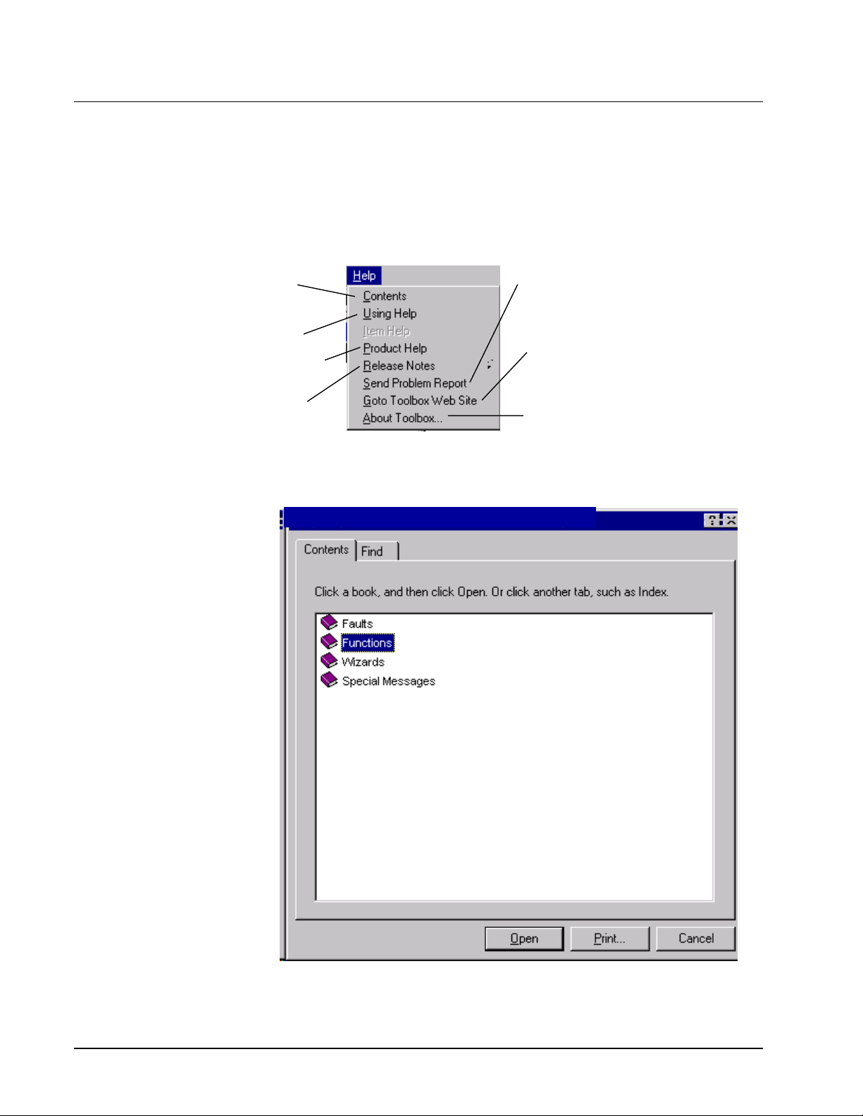
When you choose Help on the toolbox main menu bar, a drop-down menu provides
several options for finding information.
Organized Help topics, a Help Index tab,
and a Find tab for searching the Help
database.
How to find information in Help and how to
customize the toolbox Help features.
Information about faults, functions, wizards,
and special messages.
Information about the drive and toolbox
version, installation notes (compatibilities),
and requirements.
From that menu, select Product Help to access online help files that contain the
fault, function, and wizard information provided in this manual.
Help Topics: Innovation Series ACMVAC4-G Help
Drive firmware and associated
reference files may change with
product upgrades and revisions.
The information provided in this
document, GEH-6385, is current
at the time of its issue. However,
the toolbox Help files provided
with your drive may be a more
current representation of your
drive confi
uration.
Send a toolbox "bug" report or
enhancement request directly to GE
(requires that e-mail is installed).
Additional information about the toolbox
and GE contacts (requires access to the
GE intranet).
Identifies toolbox release, version, and
platform information.
1-2
••••
Chapter 1 Overview Innovation Series Medium Voltage GP Type - G Drives GEH-6385

Related Documents
If needed for supplementary information, refer to the following documents for the
Innovation Series Medium Voltage – GP Type G drives, as applicable:
GEH-6381, Installation and Startup
GEH-6382, User’s Guide
GEH-6401, Control System Toolbox
How to Get Help
If help is needed beyond the instructions provided in the documentation, contact GE
as follows:
GE Industrial Systems
Product Service Engineering
1501 Roanoke Blvd.
“+” indicates the
international access code
required when calling from
outside of the USA.
Salem, VA 24153-6492 USA
Phone: + 1 800 533 5885 (United States, Canada, Mexico)
Fax: + 1 540 387 8606 (All)
+ 1 540 378 3280 (International)
GEH-6385 Reference and Troubleshooting, 2300 V Drives Chapter 1 Overview
••••
1-3

Notes
1-4
••••
Chapter 1 Overview Innovation Series Medium Voltage GP Type - G Drives GEH-6385
Chapter 2 Faults and Troubleshooting
Introduction
For information on using the
keypad refer to the drive
User's Guide, GEH-6382.
GEH-6401 describes the
toolbox.
The drive software includes selftest diagnostics to aid in troubleshooting. When
these tests detect an unfavorable condition, they output fault indications to the
drive’s operator interfaces: the door-mounted Drive Diagnostic Interface (DDI,
referred to as the keypad) or a connected PC running the GE Control System
Toolbox (the toolbox). An operator can then use either interface to examine the fault
and clear it, as applicable.
This chapter lists and defines the relevant fault messages for the drive, with
troubleshooting suggestions. It is organized as follows:
Section Page
Introduction ........................................................................................................ 2-1
Types of Faults ................................................................................................... 2-2
Fault Indication................................................................................................... 2-2
Fault Descriptions............................................................................................... 2-3
This equipment contains a potential hazard of electric shock
or burn. Only adequately trained persons who are
thoroughly familiar with the equipment and the instructions
should maintain this equipment.
GEH-6385 Reference and Troubleshooting, 2300 V Drives Chapter 2 Faults and Troubleshooting
••••
2-1
Types of Faults
Fault Indication
There are currently two types of fault conditions:
• Alarm faults indicate conditions that you should note, but that are not serious
enough to automatically shut down or trip the drive. If the condition goes away,
some alarm faults clear themselves and the display then identifies the alarm as
brief. Otherwise, you must stop the drive to clear this type of fault.
• Trip faults indicate a more serious condition that needs to be corrected.
Therefore, it trips the drive. The drive should not be restarted until the condition
is corrected.
You can clear most faults by selecting Clear Faults on the drive’s keypad or in the
(optional) toolbox program.
The DSPX board is the
IS200DSPX Digital Signal
Processor, located in the
drive control rack.
The drive indicates a fault condition on the keypad, toolbox display, and on the
DSPX board.
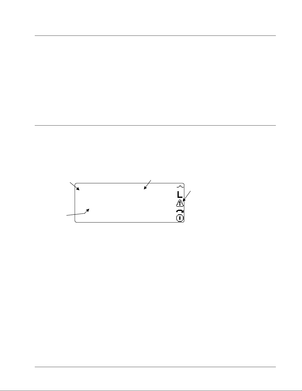
On the keypad, a fault icon appears in the right side of the display: The operator can
then use the keypad to access the fault/alarm description (see Figure 5-1) and to clear
the fault.
Fault No.
50 Trip HtSink temp low,
108 Brief DC bus voltage
12 Trip Gnd flt,
113 Trip Invalid board
Fault Behavior
Figure 2-1. Sample Fault Display Screen on Keypad
ACTIVE FAULT
--- RESET FAULTS NOW --
The toolbox uses a Windows-based PC display. When a fault occurs, the word
Alarm or Trip appears in the lower right corner of the screen. You can view a
description and clear the fault using the toolbox functions. (GE publication GEH6401 describes these tools and this feature.)
The DSPX Fault LED displays at the front of the drive’s control rack. This red
indicator is on solid for a fault and flashes for an alarm.
A fault is identified by an assigned number and abbreviated description. Both of
these are displayed when an operator examines a fault using the keypad (see Figure
2-1) or the toolbox.
Abbreviated Description
Fault Icon:
Flashing = fault
Not flashing (on steady) = alarm
Table 2-1 lists the drive faults and their probable cause.
2-2
••••
Chapter 2 Faults and Troubleshooting Innovation Series Medium Voltage GP Type - G Drives GEH-6385

Fault Descriptions
Note When troubleshooting leads to a hardware inspection or component
replacement, be sure to follow the procedures described in the drive User’s Guide,
GEH-6382. This will help ensure that the equipment operates correctly.
Table 2-1. Fault Definitions and Probable Cause
No. Name Type Description
When troubleshooting leads to a hardware inspection or
component replacement, be sure to follow the procedures
described in the drive User’s Guide, GEH-6382. This will help
prevent damage caused by incorrect installation and ensure
that the equipment operates correctly.
1 CPFP isolation lost Trip
2 Illegal seq state Trip
The CPFP isolation lost trip fault is hardware generated. The CPFP power
supply isolation card is indicating that power supply isolation to the phase
modules has been compromised. The CPFP card is designed to provide
control power to circuit cards in the high voltage compartment. This card has
a double voltage barrier that isolates the phases from each other and from the
control. This fault indicates that one of these voltage barriers has failed. This
is a dangerous situation since failure of the second barrier could cause
dangerous voltages to conduct into the control cabinet or cause a phasephase short on the CPFP card. The fault is generated when the status light
conducted via fiber from the CPFP goes out. The fiber connects CPFP (PWR
OK) to FOSA (SPARE-R). Check that the fiber is installed correctly.
Disconnect the fiber from FOSA and look for the status light traveling up the
fiber. If you do not see a light then the problem is on CPFP. If there is light
then the problem is on FOSA or BICM.
Primary causes:
CPFP power supply failure
Fiber not connected
Possible board failures:
CPFP
FOSA
BICM
Possible wiring faults:
Power distribution wiring to CPFP.
The Illegal seq state trip fault occurs when the sequencer state (variable
Sequencer state) is unrecognized. This trip may occur during system
development but should not occur in the field.
GEH-6385 Reference and Troubleshooting, 2300 V Drives Chapter 2 Faults and Troubleshooting
••••
2-3

No. Name Type Description
3 Cont failed to close Trip
4 Local flt Trip The Local flt trip fault occurs when the local permissive circuit is open and a
5 Tool requested trip Trip The Tool requested trip trip fault is generated from the engineering monitor
6 Run cmd during init Alarm
The Cont failed to close trip fault occurs when contactor A is commanded to
open or close and fails to do so within the allowed time (defined by parameter
MA pickup time).
Primary causes:
The contactor A feedback is missing or bad.
Possible configuration faults:
The allowed time for contactor A to open and close is too short. The allowed
time is represented by parameter MA pickup time.
Contactor A feedback is enabled when no contactor is present in the system.
In the absence of the contactor, parameter MA contactor fbk should be set
equal to Disable.
Related functions:
Main Contactor Configuration
Run request, Jog request, Full flux request, or diagnostic test (cell test, pulse
test, autotune) request is issued.
Possible wiring faults:
The connections to ATBA terminal board locations 8 (L115), 10 (L24), and 12
(LCOM) are missing or damaged.
The connection to backplane connector J2 is missing or damaged.
issuing the “uf” command. It is for test purposes only.
The Run cmd during init alarm occurs when a Run request, Jog request, Full
flux request, or diagnostic test (cell test, pulse test, autotune) request is issued
during drive initialization. When the alarm occurs, the request to perform a
drive action is ignored.
Primary causes:
The external application layer issues a request to perform a drive action during
drive initialization.
An external input (i.e. digital input) used to request a drive action was high
during drive initialization.
7 Over speed Trip
8 Timed over current Trip The Timed over current trip fault occurs when one of the squared phase
9 EE flash corrupted Trip
The Over speed trip fault occurs when the magnitude of speed (variable
Speed reg fbk) is greater than the over speed threshold (parameter Over
speed flt level).
Primary causes:
Motor speed is too high.
Possible configuration faults:
Parameter Over speed flt level is set too low.
Related functions:
Speed Control Fault Check
currents (variables Ia^2 filtered, Ib^2 filtered, and Ic^2 filtered) in the timed
over current detection model exceeds the timed over current threshold level.
This fault indicates that the motor has exceeded its thermal limit.
The EE flash corrupted trip fault occurs when the memory containing the drive
parameters is determined to be bad during drive initialization.
EE flash corrupted requires a hard reset to clear.
Possible board failures:
DSPX
2-4
••••
Chapter 2 Faults and Troubleshooting Innovation Series Medium Voltage GP Type - G Drives GEH-6385

No. Name Type Description
10
Run cmd w high
flux
11 EE erase failed Alarm
12 Gnd flt, coarse Trip
13 Vdc Fbk voltage
trim
14 Cap buf f in it failed Alarm The capture buffer initialization has failed to allocate enough memory to run
15 MA cont not closed Trip
Alarm
Alarm The Vdc Fbk voltage trim alarm occurs when the automatic Vdc feedback trim
The Run cmd w high flux alarm occurs when a Run request, Jog request, Full
flux request, or diagnostic test (cell test, pulse test, autotune) request is issued
and the variable Flux reference is greater than 2 percent rated flux (100%
Flux).
Primary causes:
An attempt is made to restart the drive quickly. Normally four rotor time
constants are required to allow the flux to decay after the drive stops running.
Related functions:
Sequencer Permissives
The EE erase failed trip fault occurs when the preparation of memory for the
next parameter save operation fails to happen satisfactorily. The next
parameter save operation is expected to be invalid, and the integrity of future
parameter save operations are in doubt.
EE erase failed requires a hard reset to clear.
Possible board failures:
DSPX
The Gnd flt, coarse trip fault occurs when a large ground current is detected.
The trip fault occurs when the magnitude of the sum of the three phase
currents is too large.
function on the BICM is not functioning correctly. You will not receive this
warning unless you are using drive firmware version V02.21.00B or higher
AND you have a BICMH1AB version card or higher. Older versions of
software and hardware suffer from Vdc feedback inaccuracy, which can lead
to problems in some circumstances. Getting the trim function to operate
properly is important to optimum performance of the drive. There are several
situations that can lead to this alarm.
First, make sure you have run the Cell Test Wizard (either fiber optic test or
bridge cell test) at least once when the DC link is fully discharged (<100V).
This wizard calibrates the DC bus feedback and saves a parameter in the
drive. This procedure does not need to be repeated unless hardware has
changed in the drive or the previously saved parameter was overwritten by a
parameter downloaded from the toolbox. If this procedure has not been
performed then this alarm is generated.
Second, make sure that JP1 on the BICMH1AB card has been moved to the
non-default position. This jumper enables the circuit that this alarm is
concerned with. The jumper JP1 being in the dashed-box indicates the nondefault position. The jumper being in the solid box indicates the default
position. The default position is used only when the card is placed in drives
that have software versions prior to V02.21.00B
If both if these steps fail to clear this alarm then your BICM card may be
defective.
Primary board failures
BICM
the capture buffer. The capture buffer has been disabled and will not run.
However the drive should operate normally.
A new version of firmware is required to correct this problem.
The MA cont not closed trip fault occurs when the MA feedback indicates that
the MA contactor is open when it is commanded to close.
GEH-6385 Reference and Troubleshooting, 2300 V Drives Chapter 2 Faults and Troubleshooting
••••
2-5

No. Name Type Description
16 Illegal req for xfer Alarm
17 Transfer req
aborted
18 Tune up failed Trip
19 Ext ref out of range Alarm
20 TOC pending Alarm The TOC pending alarm occurs when one of the squared phase currents
21 System flt Trip
Trip The Transfer req aborted trip fault occurs when the motor control is unable to
The Illegal req for xfer alarm occurs when a motor transfer command is issued
and a trip fault is present in the drive. The alarm may also occur when a motor
transfer command is issued at the same time a diagnostic test (cell test, pulse
test, autotune) is active.
Primary causes:
The external application layer issues an inappropriate motor transfer request.
synchronize to the utility line in the allotted time in response to a motor transfer
request.
The Tune up failed trip fault occurs when an attempt to run the motor control
tune up or the speed regulator tune up fails.
Primary causes:
The external application layer issues an inappropriate motor control tune up
request or speed regulator tune up request.
An attempt by the motor control tune up or the speed regulator tune up to
initialize the diagnostic message stack fails.
The Ext ref out of range alarm occurs when the external line reference voltage
is outside of the allowable range.
(variables Ia^2 filtered, Ib^2 filtered, and Ic^2 filtered) in the timed over current
detection model exceeds the timed over current alarm level.
This alarm indicates that the motor is nearing its thermal limit.
The System flt trip fault occurs when the system permissive circuit is open and
a Run request, Jog request, Full flux request, or diagnostic test (cell test, pulse
test, autotune) request is issued.
Possible wiring faults:
The connections to ATBA terminal board locations 2 (S115), 4 (S24), and 6
(SCOM) are missing or damaged..
22
Run before MA
closed
23 Flying restrt disabl Trip The Flying restrt disabl trip fault occurs when a Run request, Jog request, Full
Trip
The Run before MA closed trip fault occurs when a Run request, Jog request,
or Full flux request is issued to the motor control sequencer before contactor A
is closed.
Related functions:
Sequencer Permissives
Main Contactor Configuration
flux request, or diagnostic test (cell test, pulse test, autotune) request is issued
when the motor is not at zero speed.
Flying restrt disabl can be turned off and the drive allowed to start when the
motor is not at zero speed by placing the drive in flying restart mode. Flying
restart mode is enabled by setting parameter Flying restart equal to Enable fly
restart.
Related functions:
Sequencer Permissives
2-6
••••
Chapter 2 Faults and Troubleshooting Innovation Series Medium Voltage GP Type - G Drives GEH-6385

No. Name Type Description
24 Power dip Trip
25 Cur reg in limit
26 Volt reg in lim it Alarm
28 R1 meas in limit Alarm
29 R2 meas in limit Alarm The R2 meas in limit alarm occurs when the online calculation of rotor
Alarm The Cur reg in limit alarm occurs when the X and/or Y current regulator output
The Power dip trip fault occurs when the DC link voltage feedback (variable
DC bus voltage) falls below the power dip level and remains below the power
dip level longer than the power dip time.
The power dip time is configurable through parameter Power dip control.
If the DC link voltage feedback is at some moments below the power dip level
and at some moments above the power dip level, the trip fault can occur. If
over any time interval the DC link feedback spends more time below the power
dip level than above the power dip level, and the time difference is greater
than the power dip time, Power dip occurs.
Possible configuration faults:
Power dip functionality is disabled because param eter Power dip control is set
incorrectly. To enable power dip functionality parameter Power dip control
should be set equal to 0.500 sec (Enable).
Related functions:
Power Dip Protection
enter limits for more than 1 sec. It is cleared when the X and/or Y current
regulator come out of limit for more than of equal to 1 sec.
Primary causes:
The tachometer feedback is bad.
Large motor parameters errors.
Motor inverter connection opens while running.
Power dip.
Loss of current feedback.
The Volt reg in limit alarm occurs when the X and/or Y voltage regulator output
enter limits for more than 1 sec. It is cleared when the X and/or Y voltage
regulator come out of limit for more than of equal to 1 sec.
Primary causes:
Motor inverter connection opens while running.
Power dip.
Loss of voltage feedback.
The R1 meas in limit alarm occurs when the total primary resistance measured
during drive pre-flux is outside of a reasonable bound. The total primary
resistance consists of the stator and cable resistances. When the fault
condition is present, the motor control does not use the resistance
measurement.
resistance exceeds the positive or negative saturation level. The saturation
levels are 80 percent and -40 percent.
Primary causes:
The rotor resistance calculation is incorrect due a large error in motor
parameters.
30 Tach loss trip Trip The Tach loss trip fault occurs when the difference between the tachometer
feedback (variable Motor speed) and the estimated speed (variable Calculated
speed) is too large.
The trip fault can be disabled by setting parameter Tach loss fault mode equal
to Trip.
Primary causes:
The tachometer feedback is bad.
The estimated speed is incorrect due to large errors in motor parameters.
Related functions:
Tach Loss Detection
GEH-6385 Reference and Troubleshooting, 2300 V Drives Chapter 2 Faults and Troubleshooting
••••
2-7

No. Name Type Description
31 Tach loss alarm Alarm
32 IOC phase A Trip The IOC phase A trip fault is hardware generated. The trip fault occurs when
33 IOC phase B Trip
34 IOC phase C Trip
The Tach loss alarm occurs when the difference between the tachometer
feedback (variable Motor speed) and the estimated speed (variable Calculated
speed) is too large.
When the alarm occurs, the drive dynamically switches to tachless control
mode. The drive continues tachless operation until the fault is cleared by an
operator.
Tach loss fault mode can be used to change the fault behavior to trip if
required.
Primary causes:
The tachometer feedback is bad.
The estimated speed is incorrect due to large errors in motor parameters.
Related functions:
Tach Loss Detection
the current measured by the phase A shunt exceeds the instantaneous
overcurrent threshold, which is positive or negative 250 percent rated shunt
current. It also occurs within 25 microseconds when the phase A current
experiences a step change of 100 percent rated shunt. When either condition
is detected, the power bridge IGBT gating is disabled immediately.
Possible board failures:
SHCA
FOSA
BICM
HFPA (FU4)
Possible wiring faults:
Connections between FOSA and SHCA.
The IOC phase B trip fault is hardware generated. The trip fault occurs when
the current measured by the phase B shunt exceeds the instantaneous
overcurrent threshold, which is positive or negative 250 percent rated shunt
current. It also occurs within 25 microseconds when the phase B current
experiences a step change of 100 percent rated shunt. When either condition
is detected, the power bridge IGBT gating is disabled immediately.
Possible board failures:
SHCA
FOSA
BICM
HFPA (FU4)
Possible wiring faults:
Connections between FOSA and SHCA.
The IOC phase C trip fault is hardware generated. The trip fault occurs when
the current measured by the phase C shunt exceeds the instantaneous
overcurrent threshold, which is positive or negative 250 percent rated shunt
current. It also occurs within 25 microseconds when the phase C current
experiences a step change of 100 percent rated shunt. When either condition
is detected, the power bridge IGBT gating is disabled immediately.
Possible board failures:
SHCA
FOSA
BICM
HFPA (FU4)
Possible wiring faults:
Connections between FOSA and SHCA.
2-8
••••
Chapter 2 Faults and Troubleshooting Innovation Series Medium Voltage GP Type - G Drives GEH-6385

No. Name Type Description
36
BICM card clock
fail
37
Rack pwr supply
lost
38 DC bus imbalance Trip The DC bus imbalance trip fault occurs when the magnitude of the upper and
39
DC pos bus over
volt
40
DC neg bus over
volt
41 DC bus over
voltage
Trip
Trip
Trip
Trip
Trip The DC bus over voltage trip fault occurs when the DC link voltage feedback
The BICM card clock fail trip fault occurs when FPGA logic on the BICM
cannot detect the presence of either one of its clock signals. One of the clocks
it is looking for is generated by a crystal on the BICM itself and the other is
transmitted via the rack backplane from DSPX.
Primary causes:
Card or connector failure.
Possible board failures:
BICM
DSPX
CABP (Backplane)
The Rack pwr supply lost trip fault occurs when logic on the BICM cannot
detect the presence of one of the power supplies being generated by RAPA.
The power supplies monitored include P5, P15, N15 and I24. These supplies
are distributed via the backplane to control cards including BICM. I24 is also
brought to ATBA for use in customer I/O.
Primary causes:
Short across one of the monitored power supplies
Power supply module failure
Possible board failures:
BICM
RAPA
CABP (Backplane)
lower half of the DC bus circuits in the bridge differ by more than 10% of
nominal. A typical Nominal DC bus voltage would be 3500V so a difference of
around 350V would trigger this trip fault.
If the fault occurs immediately after but not during a DC bus charge cycle
completes then a ground fault in the input section of the drive should be
suspected. Check the transformer secondary windings and the input line filter
assemblies for a ground.
Primary causes:
One or more failed bleeder resistors (BRES1-6).
A ground fault in the input rectifier section
A ground fault in a transformer secondary winding.
The DC pos bus over volt trip fault is hardware generated. The trip fault
occurs when the positive DC link voltage is too large.
Possible board failures:
FOSA
DSPX
The DC neg bus over volt trip fault is hardware generated. The trip fault
occurs when the negative DC link voltage is too large.
Possible board failures:
FOSA
DSPX
(variable DC bus voltage) is too large.
The main purpose of the trip fault is to detect excessive and potentially
dangerous DC link voltages. When the over voltage condition is detected the
power bridge is shut off immediately.
Possible board failures:
FOSA
DSPX
GEH-6385 Reference and Troubleshooting, 2300 V Drives Chapter 2 Faults and Troubleshooting
••••
2-9

No. Name Type Description
42
DC bus under
voltage
43 Ground flt alm, LP Alarm The Ground flt alm, LP alarm occurs when a large ground current is detected
44 Ground flt, LP Trip
45 AC filter fuse blown Alarm The AC filter fuse blown alarm occurs when the BICM Motor Ground
Trip
The DC bus under voltage trip fault occurs when the DC link voltage feedback
(variable DC bus voltage) is too low.
The trip fault only occurs when the drive is running.
Possible board failures:
FOSA
DSPX
by the BICM Motor Ground Protection.
The alarm occurs when the BICM ground current (variable Gnd cur signal) is
greater than the BICM ground current alarm level (parameter Gnd signal alarm
on).
Ground flt alm, LP clears when the BICM ground current drops below the
BICM ground current alarm turn off level (parameter Gnd signal alarm off).
The alarm can be disabled by inhibiting BICM Motor Ground Protection
functionality. Set parameter Detector mode equal to Disable.
Possible configuration faults:
The value of the BICM ground current alarm level, represented by parameter
Gnd signal alarm on, is too low.
Possible board failures:
VATF-MID
FOSA
BICM
DSPX
The Ground flt, LP trip fault occurs when a large ground current is detected by
the BICM Motor Ground Protection.
The trip fault occurs when the BICM ground current (variable Gnd cur signal)
is greater than the BICM ground current trip fault level (parameter Gnd signal
trip lv l).
Ground flt, LP can be disabled by inhibiting BICM Motor Ground Protection
functionality. Set parameter Detector mode equal to Disable.
Possible configuration faults:
The value of the BICM ground current fault threshold, represented by
parameter Gnd signal trip lvl, is too low.
Possible board failures:
VATF-MID
FOSA
BICM
DSPX
Protection detects that the MOV fuse has blown. The trip fault occurs when
the BICM fuse circuit is open.
AC filter fuse blown can be disabled by inhibiting BICM Motor Ground
Protection functionality. Set parameter Detector mode equal to Disable.
Possible board failures:
VATF-MID
FOSA
BICM
DSPX
2-10
••••
Chapter 2 Faults and Troubleshooting Innovation Series Medium Voltage GP Type - G Drives GEH-6385

No. Name Type Description
46 X stop Trip
47
Run req & xstop
open
48 BICM card temp
low
49 HtSink DB temp
low
Trip
Trip The BICM card temp low trip fault occurs when the sensor on BICM measures
Trip The HtSink DB temp low trip fault occurs when the dynamic brake heatsink
The X stop trip fault occurs when the X stop circuit is open and when X stop is
configured as a trip fault. X stop is configured as a trip fault when parameter X
stop mode is set equal to Trip flt stop. Any other setting for parameter X stop
mode disables the X stop trip fault.
The state of the X stop circuit is determined by the value of the variable to
which parameter X stop request sel points. The X stop trip fault can be
disabled, along with all other X stop behavior, by setting parameter X stop
request sel equal to Unused.
Related functions:
Stopping Commands and Modes
The Run req & xstop open trip fault occurs when the X stop circuit is open, the
drive is stopped, and one of the following requests is issued: Run request, Jog
request, or Full flux request.
The state of the X stop circuit is determined by the value of the variable to
which parameter X stop request sel points. The trip fault can be disabled,
along with all other X stop behavior, by setting parameter X stop request sel
equal to Unused.
Related functions:
Sequencer Permissives
Stopping Commands and Modes
a temperature that is –20C or below.
BIC ambient temp is the variable being monitored to generate this fault.
Primary causes:
Failed thermal sensor on BICM.
Ambient temperature is too low.
Possible board failures:
BICM
temperature (variable DB heat sink temp) is too low.
The main purpose of this trip fault is to detect the absence of the thermal
sensor input from the heatsink.
Primary causes:
The DB heatsink thermal sensor input is not present.
No power to TFBA card or TFBA card failure.
Possible board failures:
BICM
TFBA
CPFP
Possible wiring faults:
Thermal sensor input to TFBA is missing or damaged.
Related functions:
Heatsink Thermal Protection
GEH-6385 Reference and Troubleshooting, 2300 V Drives Chapter 2 Faults and Troubleshooting
••••
2-11

No. Name Type Description
50
HtSink DS temp
low
51 HtSink A temp low Trip
52 HtSink B temp low Trip The HtSink B temp low trip fault occurs when when heatsink B temperature
53 HtSink C temp low Trip
54 Ambient temp low Trip The Ambient temp low trip fault occurs when the ambient temperature
55 AC line fuse blown Trip
56 DB resistor
overload
Trip
Trip The DB resistor overload trip fault occurs when the dynamic braking resistor
The HtSink DS temp low trip fault occurs when the diode source heatsink
temperature (variable DS heat sink temp) is too low.
The main purpose of the fault is to detect the absence of the therm al sensor
input from the heatsink.
Primary causes:
The DS heatsink thermal sensor input is not present.
No power to TFBA card or TFBA card failure.
Possible board failures:
BICM
TFBA
CPFP
Possible wiring faults:
Thermal sensor input to TFBA is missing or damaged
Related functions:
Heatsink Thermal Protection
The HtSink A temp low trip fault occurs when heatsink A temperature (variable
Heat sink A temp) is too low.
Related functions:
Heatsink Thermal Protection
(variable Heat sink B temp) is too low.
Related functions:
Heatsink Thermal Protection
The HtSink C temp low trip fault occurs when when heatsink C temperature
(variable Heat sink C temp) is too low.
Related functions:
Heatsink Thermal Protection
(variable Bridge ambient temp) is too low.
The main purpose of the trip fault is to detect the absence of the ambient
thermal sensor input.
Primary causes:
The ambient thermal sensor input is not present.
Possible board failures:
BICM
Possible wiring faults:
The thermal sensor input to backplane connector J4 pins 7 and 8 is missing or
damaged.
The AC line fuse blown trip fault occurs when one of the fuses feeding the
diode source assembly opens.
Primary causes:
Loss of I24 supply on CTBC feeding this string .
Shorted diode in source bridge.
thermal model indicates that the dynamic braking package has exceeded its
rating.
Primary causes:
Incorrect configuration of DB thermal model.
DB resistor package has not been sized correctly for application.
2-12
••••
Chapter 2 Faults and Troubleshooting Innovation Series Medium Voltage GP Type - G Drives GEH-6385

No. Name Type Description
57 DB resistor hot Alarm
58 Motor reac parms
bad
63 BICM card over
temp
64
HtSink DB over
temp
65 HtSink DS over
temp
66 HtSink A over temp Trip
67 HtSink B over temp Trip The HtSink B over temp trip fault occurs when heatsink B temperature
Trip The Motor reac parms bad trip fault occurs when the primary motor reactance
Fault The BICM card over temp trip fault occurs when the sensor on BICM
Trip
Trip The HtSink DS over temp trip fault occurs when the diode source heatsink
The DB resistor hot alarm occurs when the dynamic braking resistor thermal
model indicates that the dynamic braking package is approaching its rating.
Primary causes:
Incorrect configuration of DB thermal model.
DB resistor package is marginal for application.
parameters have values that are not appropriate relative to one another.
Primary causes:
Internal calculations are performed using Starting react Xst, Magnetizing react
Xm, Stator lkg react X1,and Rotor lkg react X2. The relationship between
these parameters should be: (Rotor lkg react X2 || Magnetizing react Xm) +
Stator lkg react X1 > Starting react Xst.
This should be corrected before attempting to run the drive.
measures a temperature above 60C. The drive control electronics cannot
operate reliably above this temperature. Reset the fault after the temperature
drops below 60C.
BIC ambient temp is the variable being monitored to generate this fault.
Primary causes:
Blocked air flow to control rack.
Control rack cooling fan failure.
Ambient temperature is too high.
Possible board failures:
BICM
The HtSink DB over temp trip fault occurs when the dynamic brake heatsink
temperature (variable DB heat sink temp) is too high.
Related functions:
Heatsink Thermal Protection
temperature (variable DS heat sink temp) is too high.
The bridge turns off in response to the fault to protect the IGBTs from thermal
damage.
Primary causes:
Airflow to the heatsink is not sufficient.
Blower is not operating correctly.
Possible board failures:
BICM
Related functions:
Heatsink Thermal Protection
The HtSink A over temp trip fault occurs when heatsink A temperature
(variable Heat sink A temp) is too high.
Related functions:
Heatsink Thermal Protection
(variable Heat sink B temp) is too high.
Related functions:
Heatsink Thermal Protection
GEH-6385 Reference and Troubleshooting, 2300 V Drives Chapter 2 Faults and Troubleshooting
••••
2-13

No. Name Type Description
68 HtSink C over temp Trip
69 BICM card hot Alarm The BICM card hot alarm occurs when the sensor on BICM measures a
70 HtSink DB temp hot Alarm
71 HtSink DS temp hot Alarm The HtSink DS temp hot alarm occurs when the diode source heatsink
72 HtSink A temp hot Alarm
73 HtSink B temp hot Alarm The HtSink B temp hot alarm occurs when heatsink B temperature (variable
The HtSink C over temp trip fault occurs when heatsink C temperature
(variable Heat sink C temp) is too high.
Related functions:
Heatsink Thermal Protection
temperature that is hot. The sensed temperature is above 55C and the control
electronics are operating outside of their design parameters. If the
temperature continues to rise and exceeds 60C, the drive will trip. This
warning is generated in order to allow time for corrective action to be taken.
BIC ambient temp is the variable being monitored to generate this alarm.
Primary causes:
Blocked air flow to control rack.
Control rack cooling fan failure.
Ambient temperature is too high.
Possible board failures:
BICM
The HtSink DB temp hot alarm occurs when the dynamic brake heatsink
temperature (variable DB heat sink temp) is high.
Related functions:
Heatsink Thermal Protection
temperature (variable DS heat sink temp) is high.
Related functions:
Heatsink Thermal Protection
The HtSink A temp hot alarm occurs when heatsink A temperature (variable
Heat sink A temp) is high.
Related functions:
Heatsink Thermal Protection
Heat sink B temp) is high.
Related functions:
Heatsink Thermal Protection
74 HtSink C temp hot Alarm The HtSink C temp hot alarm occurs when heatsink C temperature (variable
Heat sink C temp) is high.
Related functions:
Heatsink Thermal Protection
75
Switchgear not
ready
76 HtSink DB rise high Alarm
2-14
••••
Chapter 2 Faults and Troubleshooting Innovation Series Medium Voltage GP Type - G Drives GEH-6385
Alarm
The Switchgear not ready alarm occurs when the permissive string to close
the main switchgear is not present. This permissive string ends at BTBH(8)
and includes customer contacts used to open the main. The primary purpose
of the alarm is to prevent charging of the DC bus until the switchgear is ready
to close.
Primary causes:
Switchgear not racked in.
Customer switchgear permissive not met.
The HtSink DB rise high alarm occurs when the dynamic brake heatsink
temperature (variable DB heat sink temp) is too far above the ambient
temperature (variable Bridge ambient temp).
Related functions:
Heatsink Thermal Protection

No. Name Type Description
77 HtSink DS rise high Alarm
78 HtSink A rise high Alarm The HtSink A rise high alarm occurs when heatsink A temperature (variable
79 HtSink B rise high Alarm
80 HtSink C rise high Alarm
81 HtSink temp
imbalanc
82
HtSink blower
failed
83 Run permissive lost Alarm
84 Cont req while flt Alarm
Trip The HtSink temp imbalanc trip fault occurs when two of the measured heatsink
Trip
The HtSink DS rise high alarm occurs when the diode source heatsink
temperature (variable DS heat sink temp) is too far above the ambient
temperature (variable Bridge ambient temp).
Related functions:
Heatsink Thermal Protection
Heat sink A temp) is too far above the ambient temperature (variable Bridge
ambient temp).
Related functions:
Heatsink Thermal Protection
The HtSink B rise high alarm occurs when heatsink B temperature (variable
Heat sink B temp) is too far above above the ambient temperature (variable
Bridge ambient temp).
Related functions:
Heatsink Thermal Protection
The HtSink C rise high alarm occurs when heatsink A temperature (variable
Heat sink C temp) is too far above above the ambient temperature (variable
Bridge ambient temp).
Related functions:
Heatsink Thermal Protection
temperatures differ by an amount exceeding heatsink imbalance fault level.
The main purpose of the trip fault is to detect the absence of a thermal sensor
input from the heatsink, the failure of the sensor itself or heat pipe failure.
Primary causes:
A heatsink thermal sensor input is not present.
A heatsink thermal sensor is defective
The heatpipe system is defective.
Possible board failures:
BICM
Related functions:
Heatsink Thermal Protection
The HtSink blower failed trip fault occurs when the drive is running and the
cooling fans are not operating.
Primary causes:
Blower starter tripped due to blower motor overload or failure.
Related functions:
Heatsink Thermal Protection
The Run permissive lost alarm occurs when the run permissive circuit is open.
The state of the run permissive circuit is determined by the value of the
variable to which parameter Run permissive sel points. The alarm can be
disabled by setting parameter Run permissive sel equal to Unused.
Related functions:
Sequencer Permissives
The Cont req while flt alarm occurs when contactor A is commanded to close
and a trip fault is present in the drive.
GEH-6385 Reference and Troubleshooting, 2300 V Drives Chapter 2 Faults and Troubleshooting
••••
2-15

No. Name Type Description
85 Flux req while flt Alarm
86 AC line over
voltage
87 AC line voltage
high
Trip The AC line over voltage trip fault occurs when the control firmware detects
Alarm The AC line voltage high alarm occurs when the control firmware detects that
The Flux req while flt alarm occurs when a flux command is issued and a trip
fault is present in the drive. The alarm may also occur when a flux command
is issued at the same time a diagnostic test (cell test, pulse test, autotune) is
active.
Primary causes:
The external application layer issues an inappropriate flux enable request.
that the magnitude of the AC line is above the value of Line OV fault level,
which has a suggested value of 117% of nominal.
The voltage magnitude used for this comparison is a processed by a low-pass
filter. This filter is set to 1.2 rad/sec as a default, so transient over-voltages
are allowed above the threshold value without causing this trip fault.
Primary causes:
AC line voltage is excessive.
Possible configuration faults:
Source has been applied at a voltage other than that set by the factory.
Possible board failures:
VATF-SRC
FOSA
BICM
DSPX
the magnitude of the AC line is above the value of Line OV alarm level, which
has a suggested value of 112% of nominal.
The voltage magnitude used for this comparison is a low-pass filtered version
of the fastest version. The filter is set to 1.2 rad/sec as a default, so transient
voltage above the alarm turn-on value can occur without causing this alarm.
This alarm will cease once the filtered value of voltage magnitude has
decreased to below Line OV alarm clear, which has a suggested value of
110% of nominal.
Primary causes:
AC line voltage is marginally excessive.
Possible configuration faults:
Source has been applied at a voltage other than that set by the factory.
Possible board failures:
VATF-SRC
FOSA
BICM
DSPX
2-16
••••
Chapter 2 Faults and Troubleshooting Innovation Series Medium Voltage GP Type - G Drives GEH-6385

No. Name Type Description
88 AC line under volt Trip
89 AC line volts low Alarm
90 AC line over freq Trip
The AC line under volt trip fault occurs when the control firmware detects that
the magnitude of the ac line is below the value of Line UV fault level, which
has a suggested value of 50% of the nominal ac line input.
The voltage magnitude used for this comparison is a low-pass filtered version
of the signal. The filter is set to 1.2 rad/sec as a default, so transient voltages
below the alarm turn-on value can occur without causing this trip fault.
Primary causes:
AC line voltage too low.
Possible configuration faults:
Source has been applied at a voltage other than that set by the factory.
Possible board failures:
VATF-SRC
FOSA
BICM
DSPX
The AC line volts low alarm occurs when the control firmware detects that the
magnitude of the ac line is below the value of Line UV alarm level, which has a
suggested value of 88% of nominal.
The voltage magnitude used for this comparison is a low-pass filtered version
of the fastest version. The filter is set to 1.2 rad/sec as a default, so transient
voltage above the alarm turn-on value can occur without causing this alarm.
This alarm will cease once the filtered value of voltage magnitude has
increased to above the value of Line UV alarm clear, which has a suggested
value of 90% of nominal.
Primary causes:
AC line voltage is marginally low.
Possible configuration faults:
Source has been applied at a voltage other than that set by the factory.
Possible board failures:
VATF-SRC
FOSA
BICM
DSPX
The AC line over freq trip fault occurs when the control firmware detects that
the frequency of the AC line is above the value of Over freq flt level, which
has a suggested value of 125% of nominal.
The frequency value used for this comparison is a low-pass filtered version of
the fastest version. The filter is set to .2 rad/sec as a default, so transient
over-frequency values are allowed above the threshold value without causing
this trip fault.
Primary causes:
AC line frequency is excessive.
Possible configuration faults:
Source has been applied at a 60hz while the factory setup value, AC grid
frequency was at 50hz.
Possible board failures:
VATF-SRC
FOSA
BICM
DSPX
GEH-6385 Reference and Troubleshooting, 2300 V Drives Chapter 2 Faults and Troubleshooting
••••
2-17

No. Name Type Description
91 AC line freq high Alarm
92 AC line under freq Trip The AC line under freq trip fault occurs when the control firmware detects that
The AC line freq high alarm occurs when the control firmware detects that the
frequency of the AC line is above the value of Over freq alm level, which has
a suggested value of nominal frequency plus 17.3 rad/sec.
The frequency value used for this comparison is a low-pass filtered version of
the fastest version. The filter is set to .2 rad/sec as a default, so transient
over-frequency values are allowed above the threshold value without causing
this alarm.
This alarm will cease once the filtered value of filtered frequency has
decreased to below the value of Over freq alm clear, which has a suggested
value of nominal frequency plus 15.7rad/sec.
Primary causes:
AC line frequency is marginally excessive.
Possible configuration faults:
Source has been applied 60hz while the factory setup value, AC grid
frequency was at 50hz.
Possible board failures:
VATF-SRC
FOSA
BICM
DSPX
the frequency of the AC line is below the value of Under freq flt level, which
has a suggested value of nominal of 50% of nominal.
The frequency value used for this comparison is a low-pass filtered version of
the fastest version. The filter is set to .2 rad/sec as a default, so transient
under-frequency values are allowed below the threshold value without
causing this trip fault.
Primary causes:
AC line frequency is low.
Possible configuration faults:
Source has been applied at 50hz while the factory setup value, AC grid
frequency was at 60hz.
Possible board failures:
VATF-SRC
FOSA
BICM
DSPX
2-18
••••
Chapter 2 Faults and Troubleshooting Innovation Series Medium Voltage GP Type - G Drives GEH-6385

No. Name Type Description
93 AC line freq low Alarm
94 Stat charger
timeout
95 Stat charger failed Trip The Stat charger failed trip fault occurs when the static charger reports a fault
96 Switchgear failure Trip
Trip The Stat charger timeout trip fault occurs when the static charger is unable to
The AC line freq low alarm occurs when the control firmware detects that the
frequency of the AC line is below the value of Under freq alm level, which has
a suggested value of nominal minus 17.3rad/sec.
The frequency value used for this comparison is a low-pass filtered version of
the fastest version. The filter is set to .2 rad/sec as a default, so transient
under-frequency values are allowed below the threshold value without
causing this alarm.
This alarm will cease once the filtered value of filtered frequency has
increased to a value above below the value of Under freq alarm clr, which has
a suggested value of nominal frequency minus 15.7rad/sec.
Primary causes:
AC line frequency is transiently low.
Possible configuration faults:
Source has been applied at 50hz while the factory setup value, AC grid
frequency was at 60hz.
Possible board failures:
VATF-SRC
FOSA
BICM
DSPX
completely charge the DC bus. Normal charge operation terminates when the
DC bus reaches 90% of its nominal level. At this point the charger is turned
off and the switch gear is closed. If after around 70 seconds of charging the
DC bus does not reach this threshold then the trip fault is generated and the
charging sequence is aborted.
Primary causes:
Static charger failure.
DC bus capacitor defective.
during its operation. The DC bus charging procedure stops when the trip fault
occurs.
Primary causes:
Static charger failure.
The Switchgear failure trip fault occurs when the AC line switchgear does not
close in response to a close command during the bus charging sequence.
The trip fault also occurs when the switchgear opens unexpectedly during
drive operation.
Primary causes:
Switchgear defective.
Switchgear opened via external command.
Switchgear tripped.
97 Vdc <200v after
5sec
GEH-6385 Reference and Troubleshooting, 2300 V Drives Chapter 2 Faults and Troubleshooting
Trip The Vdc <200v after 5sec trip fault occurs when the static charger fails to
charge the DC bus voltage to 200 volts within 5 seconds. The DC bus
charging procedure stops when the trip fault occurs.
Primary causes:
Static charger failure.
Local Fault or System Fault Active
DC bus shorted.
DC feedback not working.
••••
2-19

No. Name Type Description
98 Ambient over temp Trip
99 Ambient temp hot Alarm The Ambient temp hot alarm occurs when the ambient temperature (variable
100 Phase A cur offset Trip The Phase A cur offset trip fault occurs when the phase A current offset
101 Phase B cur offset Trip
102 Phase C cur offset Trip
The Ambient over temp trip fault occurs when the ambient temperature
(variable Bridge ambient temp) is too high.
The main purpose of the trip fault is to use the ambient temperature
measurement to detect a condition which could endanger the power bridge.
Primary causes:
The bridge environment and running conditions cause the ambient
temperature to rise above a safe operating level.
Possible board failures:
BICM
Possible wiring faults:
The thermal sensor input to backplane connector J4 pins 7 and 8 is damaged.
Bridge ambient temp) is too high.
The main purpose of the alarm is to use the ambient temperature
measurement to detect a condition which could endanger the power bridge.
Primary causes:
The bridge environment and running conditions cause the ambient
temperature to rise above a safe operating level.
Possible board failures:
BICM
Possible wiring faults:
The thermal sensor input to backplane connector J4 pins 7 and 8 is damaged.
(variable Phs A current offset) is too large. The current offset threshold level is
1 percent of the rated shunt current (parameter IPN shunt size).
Phs A current offset is the output of an automatic current offset calculation.
The trip fault only occurs when the offset calculation is not active.
Phase A cur offset evaluates phase A current feedback information collected
while the power bridge is turned off, when current feedbacks should be zero.
It uses the information to detect power bridge and feedback circuitry problems.
The Phase B cur offset trip fault occurs when the phase B current offset
(variable Phs B current offset) is too large. The current offset threshold level is
1 percent of the rated shunt current (parameter IPN shunt size).
Phs B current offset is the output of an automatic current offset calculation.
The trip fault only occurs when the offset calculation is not active.
Phase B cur offset evaluates phase B current feedback information collected
while the power bridge is turned off, when current feedbacks should be zero.
It uses the information to detect power bridge and feedback circuitry problems.
The Phase C cur offset trip fault occurs when the phase C current offset
(variable Phs C current offset) is too large. The current offset threshold level
is 1 percent of the rated shunt current, represented by parameter IPN shunt
size.
Phs C current offset is the output of an automatic current offset calculation.
The trip fault only occurs when the offset calculation is not active.
Phase C cur offset evaluates phase C current feedback information collected
while the power bridge is turned off, when current feedbacks should be zero.
It uses the information to detect power bridge and feedback circuitry problems.
2-20
••••
Chapter 2 Faults and Troubleshooting Innovation Series Medium Voltage GP Type - G Drives GEH-6385

No. Name Type Description
103 A-B voltage offset Trip
104 B-C voltage offset Trip
105 Pulse tst config bad Trip The Pulse tst config bad trip fault occurs when the pulse test configuration
106 Ckt board list fail Trip The Ckt board list fail trip fault occurs when the electronic board ID
107 Motor volt offs high Alarm The Motor volt offs high alarm occurs when the line-line voltage offset
108 DC bus voltage low Alarm The DC bus voltage low alarm occurs when the DC link voltage feedback
The A-B voltage offset trip fault occurs when the A-B line-line voltage offset
(variable A-B, Voltage offset) is too large.
A-B, Voltage offset is the output of an automatic voltage offset calculation.
The trip fault only occurs when the offset calculation is not active.
A-B voltage offset evaluates A-B voltage feedback information collected while
the power bridge is turned off, when voltage feedbacks should be zero. It
uses the information to detect power bridge and feedback circuitry problems.
The B-C voltage offset trip fault occurs when the B-C line-line voltage offset
(variable B-C, Voltage offset) is too large.
B-C, Voltage offset is the output of an automatic voltage offset calculation.
The trip fault only occurs when the offset calculation is not active.
B-C voltage offset evaluates B-C voltage feedback information collected while
the power bridge is turned off, when voltage feedbacks should be zero. It
uses the information to detect power bridge and feedback circuitry problems.
parameters are invalid and the pulse test is invoked. The purpose of the fault
is to prevent the pulse test from running under poorly defined conditions.
Primary causes:
One or more of the following param eters is negative: Pulse 1 on time, Mid
pulse off time, Pulse 2 on time, Post pulse off time.
interrogation which happens during drive initialization fails. Each circuit board
in the rack has an electronic ID.
Ckt board list fail requires a hard reset to clear.
Primary causes:
A circuit board is not seated properly in its backplane sockets.
The electronic ID part on a circuit board has experienced a failure.
measurements are invalid when the drive is started. Generally the alarm
occurs when the drive is stopped and quickly started again.
The voltage offsets are represented by variables A-B, Voltage offset and B-C,
Voltage offset. They are the outputs of automatic voltage offset
measurements. They are valid for a certain length of time after the
measurements are performed.
The voltage offset measurements are performed when the drive is started and
enough time has elapsed to cause the previous voltage offset measurements
to be invalid. However, there is an exception to this statem ent. The offset
measurements are not performed during the flux decay time, which begins
when the drive is stopped and continues for 8 rotor time constants.
When the drive is started during the flux decay tim e, and the previous offset
measurements are invalid because too much time has elapsed since they
were performed, the Motor volt offs high alarm occurs.
Related functions:
Line-Line Voltage Protection
(variable DC bus voltage) is too low.
The alarm clears when the DC link voltage feedback rises to an acceptable
voltage, which is the under voltage threshold plus a hysteresis voltage.
DC bus voltage low only occurs when the drive is stopped.
Possible board failures:
FOSA
DSPX
GEH-6385 Reference and Troubleshooting, 2300 V Drives Chapter 2 Faults and Troubleshooting
••••
2-21

No. Name Type Description
109
Task 1 exec
overrun
110
Task 2 exec
overrun
111
Task 3 exec
overrun
112 ADL msg stack fail Alarm The ADL msg stack fail alarm occurs when an attempt by autotune or cell test
113 Invalid board set Trip The Invalid board set trip fault occurs when the electronic board ID
Alarm
Alarm
Alarm
The Task 1 exec overrun alarm occurs when Task 1 exceeds its allotted CPU
execution time. This alarm may occur during system development but should
not occur in the field.
Primary causes:
Task 1 contains too much functionality to complete in the specified execution
time.
Possible board failures:
DSPX
The Task 2 exec overrun alarm occurs when Task 2 exceeds its allotted CPU
execution time. This alarm may occur during system development but should
not occur in the field.
Primary causes:
Task 2 contains too much functionality to complete in the specified execution
time.
Task 1 contains too much functionality. Although it completes in its specified
execution time, it does not allow Task 2 to run to completion.
Possible board failures:
DSPX
The Task 3 exec overrun alarm occurs when Task 3 exceeds its allotted CPU
execution time. This alarm may occur during system development but should
not occur in the field.
Primary causes:
Task 3 contains too much functionality to complete in the specified execution
time.
Task 1 and Task 2 contain too much functionality. Although they complete in
their specified execution time, they do not allow Task 3 to run to completion.
Possible board failures:
DSPX
to allocate or free message stack memory fails. The purpose of the alarm is to
indicate failure in the use of dynamic memory with asynchronous drive
language functionality. This alarm may occur during system development but
should not occur in the field.
Primary causes:
An attempt to allocate or free memory on behalf of the ADL message stack
failed.
interrogation which happens during initialization does not produce the
expected set of circuit boards. Each circuit board in the rack has an electronic
ID which contains board type and revision information. Each Innovation
Series product has an expected set of circuit boards. If any of the expected
boards is missing, or if incorrect boards are present, the drive cannot operate
properly.
The circuit boards that the drive has identified can be obtained by making the
following GE Control System Toolbox menu selections: View, Reports, Drive
Version and Hardware Info.
Primary causes:
A circuit board which is required for the drive to operate properly is not
present.
A circuit board which should not be used in the drive is present.
A circuit board is not seated properly in its backplane socket.
The electronic ID part on a circuit board has experienced a failure.
2-22
••••
Chapter 2 Faults and Troubleshooting Innovation Series Medium Voltage GP Type - G Drives GEH-6385

No. Name Type Description
114 Ain 1 signal alarm Alarm
115 Ain 1 signal trip Trip The Ain 1 signal trip fault occurs when the level of analog input number 1
The Ain 1 signal alarm occurs when the level of analog input number 1
(variable Analog input 1) is too low. The alarm level is specified by parameter
Analog in 1 flt lev.
The alarm can occur only when parameter Analog in 1 flt mode is set equal to
Low level alarm. The alarm is disabled for any other setting for parameter
Analog in 1 flt mode.
The main purpose of Ain 1 signal alarm is to detect a low 4-20 mA signal. The
low level may indicate that a signal is missing which is required for the drive to
operate properly.
Primary causes:
The analog input number 1 signal source is absent or unhealthy.
Possible configuration faults:
The analog input 1 alarm level, represented by parameter Analog in 1 flt lev, is
set incorrectly.
The analog input number 1 gain, represented by parameter Analog in 1 gain,
is set incorrectly.
The analog input number 1 offset, represented by parameter Analog in 1
offset, is set incorrectly.
The analog input number in 1 flt mode, represented by parameter Analog in 1
flt mode, is set incorrectly.
Possible wiring faults:
The connections between the analog signal source and ATBA terminal board
locations 38 (AI1P) and 40 (AI1N) are missing or damaged.
(variable Analog input 1) is too low. The trip fault level is specified by
parameter Analog in 1 flt lev.
The trip fault can occur only when parameter Analog in 1 flt mode is set equal
to Low level trip. The trip fault is disabled for any other setting for parameter
Analog in 1 flt mode.
The main purpose of Ain 1 signal trip is to detect a low 4-20 mA signal. The
low level may indicate that a signal is missing which is required for the drive to
operate properly.
Primary causes:
The analog input number 1 signal source is absent or unhealthy.
Possible configuration faults:
The analog input 1 trip fault level, represented by parameter Analog in 1 flt lev,
is set incorrectly.
The analog input number 1 gain, represented by parameter Analog in 1 gain,
is set incorrectly.
The analog input number 1 offset, represented by parameter Analog in 1
offset, is set incorrectly.
The analog input number in 1 flt mode, represented by parameter Analog in 1
flt mode, is set incorrectly.
Possible wiring faults:
The connections between the analog signal source and ATBA terminal board
locations 38 (AI1P) and 40 (AI1N) are missing or damaged.
GEH-6385 Reference and Troubleshooting, 2300 V Drives Chapter 2 Faults and Troubleshooting
••••
2-23

No. Name Type Description
116 Ain 2 signal alarm Alarm
117 Ain 2 signal trip Trip The Ain 2 signal trip fault occurs when the level of analog input number 2
118 Illegal req for sby Alarm The Illegal req for sby alarm occurs when a Standby command is issued and a
The Ain 2 signal alarm occurs when the level of analog input number 2
(variable Analog input 2) is too low. The alarm level is specified by parameter
Analog in 2 flt lev.
The alarm can occur only when parameter Analog in 2 flt mode is set equal to
Low level alarm. The fault is disabled for any other setting for param eter
Analog in 2 flt mode.
The main purpose of Ain 2 signal alarm is to detect a low 4-20 mA signal. The
low level may indicate that a signal is missing which is required for the drive to
operate properly.
Primary causes:
The analog input number 2 signal source is absent or unhealthy.
Possible configuration faults:
The analog input 2 alarm level, represented by parameter Analog in 2 flt lev, is
set incorrectly.
The analog input number 2 gain, represented by parameter Analog in 2 gain,
is set incorrectly.
The analog input number 2 offset, represented by parameter Analog in 2
offset, is set incorrectly.
The analog input number in 2 flt mode, represented by parameter Analog in 2
flt mode, is set incorrectly.
Possible wiring faults:
The connections between the analog signal source and ATBA terminal board
locations 44 (AI2P) and 46 (AI2N) are missing or damaged.
(variable Analog input 2) is too low. The trip fault level is specified by
parameter Analog in 2 flt lev.
The trip fault can occur only when parameter Analog in 2 flt mode is set equal
to Low level trip. The trip fault is disabled for any other setting for parameter
Analog in 2 flt mode.
The main purpose of Ain 2 signal trip is to detect a low 4-20 mA signal. The
low level may indicate that a signal is missing which is required for the drive to
operate properly.
Primary causes:
The analog input number 2 signal source is absent or unhealthy.
Possible configuration faults:
The analog input 2 trip fault level, represented by parameter Analog in 2 flt lev,
is set incorrectly.
The analog input number 2 gain, represented by parameter Analog in 2 gain,
is set incorrectly.
The analog input number 2 offset, represented by parameter Analog in 2
offset, is set incorrectly.
The analog input number in 2 flt mode, represented by parameter Analog in 2
flt mode, is set incorrectly.
Possible wiring faults:
The connections between the analog signal source and ATBA terminal board
locations 44 (AI2P) and 46 (AI2N) are missing or damaged.
trip fault is present in the drive. The alarm may also occur when a Standby
command is issued at the same time a diagnostic test (cell test, pulse test,
autotune) is active.
Primary causes:
The external application layer issues an inappropriate standby request.
2-24
••••
Chapter 2 Faults and Troubleshooting Innovation Series Medium Voltage GP Type - G Drives GEH-6385

No. Name Type Description
119
Start permissive
bad
121 DBS1 IGDM card flt Trip
122 DBS2 IGDM card flt Trip
Alarm
The Start permissive bad alarm occurs when the start permissive circuit is
open and the drive is stopped. The state of the start permissive circuit is
determined by the value of the variable which parameter Start permissive sel
selects. The alarm can be disabled by setting parameter Start permissive sel
equal to Unused.
Related functions:
Sequencer Permissives
The DBS1 IGDM card flt trip fault is hardware generated. The trip fault occurs
when the bridge control has lost communication with the indicated IGDM
module. This communication occurs via fiber optic cable between the FOSA
and the IGDM. During normal operation the IGDM transmits continuous light
back to FOSA. Any loss of this signal triggers this trip fault.
Several unrelated situations can cause the light to stop transmitting. Run the
Cell Test Wizard to identify any failed devices.
Primary causes:
CPFP power supply failure
IGDM failure
A desat fault on the indicated IGBT was detected.
Possible board failures:
IGDM
CPFP
FOSA
BICM
Possible wiring faults:
Fiber optic connection between FOSA and IGDM
Power distribution wiring from CPFP.
The DBS2 IGDM card flt trip fault is hardware generated. The trip fault occurs
when the bridge control has lost communication with the indicated IGDM
module. This communication occurs via fiber optic cable between the FOSA
and the IGDM. During normal operation the IGDM transmits continuous light
back to FOSA. Any loss of this signal triggers this trip fault.
Several unrelated situations can cause the light to stop transmitting. Run the
Cell Test Wizard to identify any failed devices.
Primary causes:
CPFP power supply failure
IGDM failure
A desat fault on the indicated IGBT was detected.
Possible board failures:
IGDM
CPFP
FOSA
BICM
Possible wiring faults:
Fiber optic connection between FOSA and IGDM
Power distribution wiring from CPFP.
GEH-6385 Reference and Troubleshooting, 2300 V Drives Chapter 2 Faults and Troubleshooting
••••
2-25

No. Name Type Description
123 AS1 IGDM card flt Trip
124 AS2 IGDM card flt Trip The AS2 IGDM card flt trip fault is hardware generated. The trip fault occurs
The AS1 IGDM card flt trip fault is hardware generated. The trip fault occurs
when the bridge control has lost communication with the indicated IGDM
module. This communication occurs via fiber optic cable between the FOSA
and the IGDM. During normal operation the IGDM transmits continuous light
back to FOSA. Any loss of this signal triggers this trip fault.
Several unrelated situations can cause the light to stop transmitting. Run the
Cell Test Wizard to identify any failed devices.
Primary causes:
CPFP power supply failure
IGDM failure
A desat fault on the indicated IGBT was detected.
Possible board failures:
IGDM
CPFP
FOSA
BICM
Possible wiring faults:
Fiber optic connection between FOSA and IGDM
Power distribution wiring from CPFP.
2-26
••••
Chapter 2 Faults and Troubleshooting Innovation Series Medium Voltage GP Type - G Drives GEH-6385

No. Name Type Description
125 AS3 IGDM card flt Trip
126 AS4 IGDM card flt Trip The AS4 IGDM card flt trip fault is hardware generated. The trip fault occurs
The AS3 IGDM card flt trip fault is hardware generated. The trip fault occurs
when the bridge control has lost communication with the indicated IGDM
module. This communication occurs via fiber optic cable between the FOSA
and the IGDM. During normal operation the IGDM transmits continuous light
back to FOSA. Any loss of this signal triggers this trip fault.
Several unrelated situations can cause the light to stop transmitting. Run the
Cell Test Wizard to identify any failed devices.
Primary causes:
CPFP power supply failure
IGDM failure
A desat fault on the indicated IGBT was detected.
Possible board failures:
IGDM
CPFP
FOSA
BICM
Possible wiring faults:
Fiber optic connection between FOSA and IGDM
Power distribution wiring from CPFP.
GEH-6385 Reference and Troubleshooting, 2300 V Drives Chapter 2 Faults and Troubleshooting
••••
2-27

No. Name Type Description
127 BS1 IGDM card flt Trip
128 BS2 IGDM card flt Trip The BS2 IGDM card flt trip fault is hardware generated. The trip fault occurs
The BS1 IGDM card flt trip fault is hardware generated. The trip fault occurs
when the bridge control has lost communication with the indicated IGDM
module. This communication occurs via fiber optic cable between the FOSA
and the IGDM. During normal operation the IGDM transmits continuous light
back to FOSA. Any loss of this signal triggers this trip fault.
Several unrelated situations can cause the light to stop transmitting. Run the
Cell Test Wizard to identify any failed devices.
Primary causes:
CPFP power supply failure
IGDM failure
A desat fault on the indicated IGBT was detected.
Possible board failures:
IGDM
CPFP
FOSA
BICM
Possible wiring faults:
Fiber optic connection between FOSA and IGDM
Power distribution wiring from CPFP.
2-28
••••
Chapter 2 Faults and Troubleshooting Innovation Series Medium Voltage GP Type - G Drives GEH-6385

No. Name Type Description
129 BS3 IGDM card flt Trip
130 BS4 IGDM card flt Trip The BS4 IGDM card flt trip fault is hardware generated. The trip fault occurs
The BS3 IGDM card flt trip fault is hardware generated. The trip fault occurs
when the bridge control has lost communication with the indicated IGDM
module. This communication occurs via fiber optic cable between the FOSA
and the IGDM. During normal operation the IGDM transmits continuous light
back to FOSA. Any loss of this signal triggers this trip fault.
Several unrelated situations can cause the light to stop transmitting. Run the
Cell Test Wizard to identify any failed devices.
Primary causes:
CPFP power supply failure
IGDM failure
A desat fault on the indicated IGBT was detected.
Possible board failures:
IGDM
CPFP
FOSA
BICM
Possible wiring faults:
Fiber optic connection between FOSA and IGDM
Power distribution wiring from CPFP.
GEH-6385 Reference and Troubleshooting, 2300 V Drives Chapter 2 Faults and Troubleshooting
••••
2-29

No. Name Type Description
131 CS1 IGDM card flt Trip
132 CS2 IGDM card flt Trip The CS2 IGDM card flt trip fault is hardware generated. The trip fault occurs
The CS1 IGDM card flt trip fault is hardware generated. The trip fault occurs
when the bridge control has lost communication with the indicated IGDM
module. This communication occurs via fiber optic cable between the FOSA
and the IGDM. During normal operation the IGDM transmits continuous light
back to FOSA. Any loss of this signal triggers this trip fault.
Several unrelated situations can cause the light to stop transmitting. Run the
Cell Test Wizard to identify any failed devices.
Primary causes:
CPFP power supply failure
IGDM failure
A desat fault on the indicated IGBT was detected.
Possible board failures:
IGDM
CPFP
FOSA
BICM
Possible wiring faults:
Fiber optic connection between FOSA and IGDM
Power distribution wiring from CPFP.
2-30
••••
Chapter 2 Faults and Troubleshooting Innovation Series Medium Voltage GP Type - G Drives GEH-6385

No. Name Type Description
133 CS3 IGDM card flt Trip
134 CS4 IGDM card flt Trip The CS4 IGDM card flt trip fault is hardware generated. The trip fault occurs
The CS3 IGDM card flt trip fault is hardware generated. The trip fault occurs
when the bridge control has lost communication with the indicated IGDM
module. This communication occurs via fiber optic cable between the FOSA
and the IGDM. During normal operation the IGDM transmits continuous light
back to FOSA. Any loss of this signal triggers this trip fault.
Several unrelated situations can cause the light to stop transmitting. Run the
Cell Test Wizard to identify any failed devices.
Primary causes:
CPFP power supply failure
IGDM failure
A desat fault on the indicated IGBT was detected.
Possible board failures:
IGDM
CPFP
FOSA
BICM
Possible wiring faults:
Fiber optic connection between FOSA and IGDM
Power distribution wiring from CPFP.
GEH-6385 Reference and Troubleshooting, 2300 V Drives Chapter 2 Faults and Troubleshooting
••••
2-31

No. Name Type Description
135 AC line transient Alarm
The AC line transient alarm occurs as a result of significant phase lock loop
error or significant phase imbalance.
A phase imbalance signal is calculated by subtracting a control calculated
threshold from a filtered signal which is formed by filtering the sum of two
signals. One of these signals is the phase lock loop error and the other is the
error between the demodulated real component of line voltage and the
measured magnitude of the line.
The calculated threshold phase imbalance level which is computed by the
control is based on the magnitude of the input line voltage. This calculated
phase imbalance threshold represents a phase imbalance of about 18% or a
phase lock loop error of about 6.7 degrees. The phase imbalance signal
which is a result of the previously mentioned subtraction is equal to about
18% imbalance when it becomes positive.
The phase imbalance signal feeds an integrator designed to cause the AC line
transient alarm when the threshold has been exceeded for a very short time.
That amount of time is dependent upon the amount of the phase imbalance,
but the alarm will occur eventually if the imbalance signal remains positive.
Primary causes:
AC line disturbances.
Transient phase imbalances.
Weak control of frequency on diesel generator sets or gas turbine generator
sets.
Very fast voltage magnitude changes.
Damaged reactor or transformer
Possible board failures:
VATF-SRC
FOSA
BICM
DSPX
2-32
••••
Chapter 2 Faults and Troubleshooting Innovation Series Medium Voltage GP Type - G Drives GEH-6385

No. Name Type Description
136 AC line watchdog Trip
137 AC line rev phs seq Trip
The AC line watchdog trip fault will occur when the AC line transient alarm
persists for about one second. Both the trip fault and the alarm are a result of
significant phase lock loop error or significant phase imbalance.
A phase imbalance signal is calculated by subtracting a control calculated
threshold from a filtered signal which is formed by filtering the sum of two
signals. One of these signals is the phase lock loop error and the other is the
error between the demodulated real component of line voltage and the
measured magnitude of the line.
The calculated threshold phase imbalance level which is computed by the
control is based on the magnitude of the input line voltage. This calculated
phase imbalance threshold represents a phase imbalance of about 18% or a
phase lock loop error of about 6.7 degrees. The phase imbalance signal
which is a result of the previously mentioned subtraction is equal to about
18% imbalance when it becomes positive.
The phase imbalance signal feeds an integrator designed to cause the AC line
transient alarm when the threshold has been exceeded for a very short time.
That amount of time is dependent upon the amount of the phase imbalance,
but the alarm will occur eventually if the imbalance signal remains positive. If
the alarm persists continuously for about one second, the AC line watchdog
trip fault will occur.
Primary causes:
AC line disturbances.
Transient phase imbalances.
Weak control of frequency on diesel generator sets or gas turbine generator
sets.
Very fast voltage magnitude changes.
Damaged reactor or transformer
Possible board failures:
VATF-SRC
FOSA
BICM
DSPX
The AC line rev phs seq trip fault occurs when the control senses that the
rotation of the AC line is opposite of what is expected. This condition is
checked only one time after the control is powered up. When the phase lock
loop locks for the first time, just after the charging sequence has begun, the
sign of PLL frequency is checked against the expected sign. The expected
sign is determined by the setting of Phase rotation req. If Forward sequence
is selected, the sign of PLL frequency is expected to be positive, otherwise, it
must be negative. If the expected sign is not found, the trip fault is given. AC
line rev phs seq requires a hard reset to clear.
Before changing Phase rotation req, review the rotation of any AC cooling
pumps or blowers in the drive. Incorrect phase sequence can lead to
ineffective air or water flow in the cooling system.
Primary causes:
Control senses wrong phase sequence.
Possible board failures:
VATF-SRC
FOSA
BICM
DSPX
Possible wiring faults:
Main AC input lines to source are not in correct phase sequence.
Sensing wires to FOSA are in wrong sequence.
GEH-6385 Reference and Troubleshooting, 2300 V Drives Chapter 2 Faults and Troubleshooting
••••
2-33

No. Name Type Description
138 AC line vfb offset Trip
139 AC line failed Trip
140 Xfrmr over temp Trip
141 Xfrmr temp hot Alarm The Xfrmr temp hot alarm occurs when the transform er over temperature
142 Motor over temp Trip
143 Motor temp hot Alarm
144 Unrecognized IPN Trip
The AC line vfb offset trip fault occurs when the voltage feedback offset being
calculated for line voltage feedbacks is above the allowable threshold. The
system integrates the voltages seen on the AC input terminals. The results of
this integration should be near zero since the input waveform is a sine wave.
If the input line-line voltages integrate to a non-zero value above a predefined
threshold this trip fault is generated.
Primary causes:
Bad VCO Circuit.
Incorrect sensor wiring.
Large DC current component through transformer.
Possible board failures:
VATF-SRC
FOSA
BICM
DSPX
Possible wiring faults:
Check wiring of VATF-SRC sensor inputs to phase leg.
The AC line failed trip fault occurs when the phase lock loop fails to
synchronize during the start up sequence.
Primary causes:
The AC line is missing.
There is a large AC line imbalance.
There is a blown fuse.
The Xfrmr over temp trip occurs when the transform er over temperature circuit
is open. The control input which points to the over temperature circuit is
selected by parameter Xfrmr OT fault sel.
Xfrmr over temp can be disabled by setting parameter Xfrmr OT fault sel equal
to Unused.
circuit is open. The control input which points to the over temperature circuit is
selected by parameter Xfrmr OT fault sel.
Xfrmr temp hot can be disabled by setting param eter Xfrmr OT fault sel equal
to Unused.
The Motor over temp trip fault occurs when the motor overtemperature circuit
is open. The state of the motor overtemperature circuit is selected by
parameter Motor OT fault sel.
Motor over temp can be disabled by setting param eter Motor OT fault sel
equal to Unused.
Related functions:
Motor Overtemperature Detection
The Motor temp hot trip fault occurs when the motor overtem perature circuit is
open. The state of the motor overtemperature circuit is selected by parameter
Motor OT fault sel.
Motor temp hot can be disabled by setting parameter Motor OT fault sel equal
to Unused.
Related functions:
Motor Overtemperature Detection
The Unrecognized IPN trip fault occurs when the specified Intelligent Part
Number (IPN) is not a valid combination of fields for the Innovation Series
product. The IPN should correspond to the drive nameplate.
Unrecognized IPN requires a hard reset to clear.
2-34
••••
Chapter 2 Faults and Troubleshooting Innovation Series Medium Voltage GP Type - G Drives GEH-6385

No. Name Type Description
145
Customer use NC
flt
146 Customer use NC
alm
147
Customer use NO
flt
148
Customer use NO
alm
149 Sat curve data bad Trip The Sat curve data bad trip fault occurs when the flux saturation curve is not
150 Rated flux data bad Trip
Trip
Alarm The Customer use NC alm alarm occurs when the customer normally closed
Trip
Alarm
The Customer use NC flt trip fault occurs when the customer normally closed
circuit is open. The state of the normally closed circuit is selected by
parameter User NC fault sel.
circuit is open. The state of the normally closed circuit is selected by
parameter User NC fault sel.
The Customer use NO flt trip fault occurs when the customer normally open
circuit is closed. The state of the normally open circuit is selected by
parameter User NO fault sel.
The Customer use NO alm alarm occurs when the customer normally open
circuit is closed. The state of the normally open circuit is selected by
parameter User NO fault sel.
monotonic.
Primary causes:
The saturation curve data entered by the operator is bad.
The saturation curve data calculated by autotune is bad.
Possible configuration faults:
One or more of the saturation curve parameters is bad. The saturation curve
parameters are Flux curve amps 1, Flux curve amps 2, Flux curve amps 3,
Flux curve amps 4, Flux curve amps 5, Flux curve voltage 1, Flux curve
voltage 2, Flux curve voltage 3, Flux curve voltage 4, and Flux curve voltage 5.
The Rated flux data bad trip fault occurs when the motor control calculation of
rated flux (variable 100% Flux) does not converge to a stable value.
151 Leakage curve bad Trip The Leakage curve bad trip fault occurs when the leakage flux curve is not
monotonic (i.e. Point 1 < point 2 < point 3 < point 4 < point 5).
Primary causes:
The calculated leakage curve has been derived from bad motor reactance
data.
The leakage curve data entered by the operator is bad.
The leakage curve data calculated by autotune is bad.
Possible configuration faults:
When the leakage curve is not entered specifically point-by-point (see below)
one is calculated from Starting react Xst, Magnetizing react Xm, Stator lkg
react X1, and Rotor lkg react X2. The relationship between these parameters
should be: (Rotor lkg react X2 || Magnetizing react Xm) + Stator lkg react X1
> Starting react Xst. If Motor reac parms bad fault is also present, this is the
likely cause.
When the leakage curve is not entered specifically point-by-point, one or more
of the leakage curve parameters is bad. The leakage curve parameters are
Lkg flux current 1, Lkg flux current 2, Lkg flux current 3, Lkg flux current 4, Lkg
flux current 5, Lkg flux voltage 1, Lkg flux voltage 2, Lkg flux voltage 3, Lkg flux
voltage 4, and Lkg flux voltage 5. If the leakage parameters are not set, the
leakage curve is determined as above, or as the results of autotune.
152 Invalid Time Base Trip
The Invalid Time Base trip fault occurs when the execution time base is
invalid. Parameter Exec time/Chop freq contains valid choices for the time
base.
Invalid Time Base requires a hard reset to clear.
GEH-6385 Reference and Troubleshooting, 2300 V Drives Chapter 2 Faults and Troubleshooting
••••
2-35

No. Name Type Description
153 DSPx Watchdog
154 Reverse rotation Trip The Reverse rotation trip fault occurs when the motor shaft is rotating opposite
155 Failure to rotate Trip
156 Loss of spd control Alarm
157 Bic Watchdog Trip The Bic Watchdog trip fault occurs when the BICM stops seeing a watchdog
158 Bic watchdog echo Trip
Trip
Locke
d
The DSPx Watchdog trip fault occurs when the DSPX EPLD stops seeing a
watchdog toggle bit from the processor. A hard reset occurs and the fault is
declared at initialization.
DSPx Watchdog requires a hard reset to clear.
Possible board failures:
DSPX
to the requested direction.
Related functions:
Speed Control Fault Check
The Failure to rotate trip fault occurs when speed regulator error grows large
while the speed feedback is small.
Related functions:
Speed Control Fault Check
The Loss of spd control trip fault occurs when the speed regulator error is too
large.
Related functions:
Speed Control Fault Check
toggle bit from the DSPX. When the drive is running, BICM monitors a toggle
bit being manipulated by DSPX. If DSPX does not toggle the bit on BICM
within a predefined time interval, the BICM declares a fault and disables the
bridge. This indicates that the processor cannot communicate reliably with the
bridge interface card.
Bic Watchdog requires a hard reset to clear.
Possible configuration faults:
The connected drive is a simulator but Simulate mode act is equal to False.
Set Simulate mode equal to Yes to correct the problem.
Possible board failures:
BICM
DSPX
CABP (backplane)
The Bic watchdog echo trip fault occurs when the DSPX stops seeing the echo
of the watchdog toggle bit that it writes to the BICM. This indicates that the
processor cannot communicate reliably with the bridge interface card.
Primary Causes:
Bent backplane connector pins or poorly seated cards.
Possible board failures:
BICM
DSPX
CABP (backplane)
160 LAN trip request Trip The LAN trip request trip fault occurs when a request for a trip fault is received
from the LAN by assertion of the reference Boolean signal Trip request, lan.
161 LAN alarm request Alarm The LAN alarm request alarm occurs when a request for an alarm is received
from the LAN by assertion of the reference Boolean signal Alarm request, lan.
2-36
••••
Chapter 2 Faults and Troubleshooting Innovation Series Medium Voltage GP Type - G Drives GEH-6385

No. Name Type Description
162
LAN watchdog
alarm
163
Restrictd fcn
enabld
164 LAN heartbeat trip Trip The LAN heartbeat trip occurs when all of the following conditions are present:
165
LAN heartbeat
alarm
166
Requird Parm
Missing
Alarm
Alarm
Alarm
Trip
The LAN watchdog alarm occurs when the connection between DSPX and the
Application/LAN interface becomes invalid. This includes one of the following
conditions, depending upon the selection of Network interface:
The Application/LAN interface Dual-Port RAM watchdog stops.
The ISBus fram es stop.
The alarm is declared after the condition persists for several hundred
microseconds.
The Restrictd fcn enabld alarm occurs when the selected execution time base
in the parameter Exec time/Chop freq restricts certain drive functionality due to
timing limitations, or the ISBus network is selected by the Network interface
parameter and the DSPX hardware does not support ISBus. Certain functions
that are presently enabled will not run.
Possible configuration faults:
Execution time base is too low. Select alternate tim e base in param eter Exec
time/Chop freq.
LAN is enabled, but will not operate. Disable LAN by setting parameter
Network interface to None.
ISBus is selected, but will not operate. Deselect ISBus by setting parameter
Network interface, or replace the DSPX HIA with a DSPX H1B.
Non-zero value is entered in Parameter LAN heartbeat time.
The signal (Heartbeat ref, lan) fails to transition within in that time.
The trip behavior is enabled by Parameter LAN trips inhibit.
The LAN connection ok condition was previously detected.
The LAN heartbeat alarm occurs when all of the following conditions are
present:
Non-zero value is entered in Parameter LAN heartbeat time.
The signal (Heartbeat ref, lan) fails to transition within in that time.
Either the trip behavior is inhibited by Parameter LAN trips inhibit, or the trip
behavior is enabled but the LAN connection ok condition was not previously
detected.
The Requird Parm Missing trip fault occurs when one of the required
parameters either is not entered, “No Value” or has a value of zero. Check the
following values, which can be found in the commissioning wizard.
Primary causes:
Motor rated voltage, Not entered
Motor rated freq, Not entered
Motor rated current, Not entered
Motor rated rpm, Not entered
Motor rated power, Not entered
Motor service factor, Not entered
167 Version mismatch Trip The Version mismatch trip fault occurs at initialization when the drive pattern
detects a product or version mismatch with the parameters stored in nonvolatile RAM. Download parameters to fix.
168 System ISBus error Alarm The System ISBus error alarm occurs when an ISBus fault is detected in the
DSPX control. The variable Sys ISBus error reg contains the bit-coded value
of the last ISBus fault detected; each bit indicates a particular ISBus fault seen
by the control. The variable Sys ISBus error cnt increments upon fault
detection.
Record the value of Sys ISBus error reg to assist factory troubleshooting
efforts. Monitor the progression of Sys ISBus error cnt to obtain an indication
of the rate of occurrence of fault conditions.
Transient occurrence of this alarm upon initialization of the interface is
expected.
GEH-6385 Reference and Troubleshooting, 2300 V Drives Chapter 2 Faults and Troubleshooting
••••
2-37

No. Name Type Description
169 Frame PLL not OK Alarm
The Frame PLL not OK alarm occurs when phase-lock between the DSPX
control and the System ISBus or (local ACL) is not assured. Detection of the
fault is enabled when the parameter Netw ork int erface is configured to select
an interface for which synchronized operation is supported. The presence of
this alarm indicates that data coherency is compromised.
Verify the integrity of IsBus connections and configurations. If this alarm
persists in the absence of any other interface faults, then verify that LAN frame
time is consistent with that of the host, and confirm the absence of overrides,
particularly regarding the Frame phaselock loop and DSPX timebase.
Transient occurrence of this alarm upon initialization of the interface is
expected.
2-38
••••
Chapter 2 Faults and Troubleshooting Innovation Series Medium Voltage GP Type - G Drives GEH-6385

Chapter 3 Paramters/Functions
Introduction
Chapter 4 describes wizards.
Application firmware consists of coordinated blocks of code called functions. Each
function performs a specific task in controlling the drive. Parameters are adjustable
values within a function that allow you to configure and adjust the drive behavior.
Parameters can be set and modified using wizards within the keypad and the optional
toolbox.
The following is a list of the drive parameters and functionsIt is organized as
follows:
Section Page
Introduction ........................................................................................................ 3-1
Diagnostic and Utility Functions ......................................................................... 3-4
Diagnostic and Utility Overview................................................................... 3-4
Capture Buffer ............................................................................................. 3-4
General Purpose Constants ..........................................................................3-10
General Purpose Filters ...............................................................................3-11
Oscillator ....................................................................................................3-12
Position Feedback .......................................................................................3-13
Predefined Constants...................................................................................3-14
Signal Level Detector (SLD) .......................................................................3-15
Simulator ....................................................................................................3-18
Control Diagnostic Variables.......................................................................3-19
Line Simulator ............................................................................................3-19
Drive Configuration Functions ...........................................................................3-20
Intelligent Part Number (IPN)......................................................................3-20
Primary Motor & Application Data..............................................................3-21
General Setup Functions.....................................................................................3-24
Keypad Overview........................................................................................3-24
Keypad Contrast Adjustment.......................................................................3-25
Keypad Meter Configuration .......................................................................3-25
Keypad Security Configuration....................................................................3-27
Language and Units Presentation.................................................................3-28
Language Display........................................................................................3-29
I/O Functions.....................................................................................................3-30
Analog and Digital I/O Testing....................................................................3-30
Analog Inputs/Outputs and Mapping............................................................3-32
Digital Inputs/Outputs and Mapping ............................................................3-33
LAN Functions ..................................................................................................3-34
GEH-6385 Reference and Troubleshooting, 2300 V Drives Chapter 3 Paramters/Functions
••••
3-1

LAN Overview............................................................................................3-34
Frame Phaselock Loop ................................................................................3-34
LAN Configuration and Health....................................................................3-35
LAN Signal Map.........................................................................................3-38
Motor Control Functions....................................................................................3-44
Motor Control Overview .............................................................................3-44
Flux Curve ..................................................................................................3-45
Leakage Inductance Curve...........................................................................3-46
Line Transfer ..............................................................................................3-46
Motor Equivalent Circuit.............................................................................3-48
Motor Temperature Estimation....................................................................3-49
Power Dip Protection ..................................................................................3-49
Tach Loss Detection....................................................................................3-50
Protective Functions...........................................................................................3-52
Custom User Faults.....................................................................................3-52
DC Link Protection .....................................................................................3-52
Ground Fault Protection (Fast).....................................................................3-54
Hardware Fault Strings................................................................................3-55
Heatsink Thermal Protection .......................................................................3-56
Line-Line Voltage Protection.......................................................................3-58
Motor Overtemperature Detection ...............................................................3-59
Phase Current Protection .............................................................................3-60
Timed Overcurrent Detection ......................................................................3-61
Transformer Overtemperature Detection......................................................3-65
Motor Ground Protection.............................................................................3-66
Phase Imbalance Monitor ............................................................................3-68
Line Monitor...............................................................................................3-70
Phase Lock Loop.........................................................................................3-72
Sequencer Functions ..........................................................................................3-74
Sequencer Overview....................................................................................3-74
Fault Reset Logic ........................................................................................3-74
Sequencer Permissives.................................................................................3-76
Stopping Commands and Modes..................................................................3-78
Sequencer Commands.................................................................................3-82
Sequencer Status.........................................................................................3-85
Main Contactor Configuration.....................................................................3-87
Speed Reference Functions.................................................................................3-89
Critical Speed Avoidance ............................................................................3-89
Local Speed Reference................................................................................3-90
Minimum Speed Limit ................................................................................3-91
Remote Speed Reference.............................................................................3-92
Speed Reference Generation........................................................................3-93
Speed Reference Ramp................................................................................3-94
Speed Reference Reverse.............................................................................3-97
Speed/Torque Control Functions ........................................................................3-99
Droop..........................................................................................................3-99
Motor Control Interface.............................................................................3-100
Speed Control Fault Check........................................................................3-103
Speed Feedback Calculation......................................................................3-105
Speed/Torque Overview............................................................................3-106
Speed/Torque Regulator............................................................................3-107
System Data Parameters...................................................................................3-112
Exec time/Chop freq..................................................................................3-112
Motor ctrl alg sel.......................................................................................3-112
Motor efficiency........................................................................................3-113
Motor service factor ..................................................................................3-114
3-2
••••
Chapter 3 Paramters/Functions Innovation Series Medium Voltage GP Type - G Drives GEH-6385

Motor winding cfg.....................................................................................3-114
Preflux Forcing .........................................................................................3-114
GEH-6385 Reference and Troubleshooting, 2300 V Drives Chapter 3 Paramters/Functions
••••
3-3

Diagnostic and Utility Functions
Diagnostic and Utility Overview
The Innovation Series products contain a number of diagnostic functions. More
information is available for the following topics.
• Capture Buffer
• General Purpose Constants
• General Purpose Filters
• Oscillator
• Position Feedback
• Predefined Constants
• Signal Level Detector (SLD)
• Simulator
Capture Buffer
The Innovation Series capture buffer is used to collect coherent data at a specified
rate in the drive. The capture buffer is circular, and will collect a fixed number of
samples of each data channel before overwriting the oldest data. The capture buffer
can be triggered on any available variable signal in the drive by using a Boolean
trigger mode or comparison to a value. The capture buffer will also trigger on a Trip
fault. It is useful for capturing drive variables for troubleshooting field problems and
capturing specific drive events. The Trend Recorder can display the capture buffer
output.
Function Inputs
The following table specifies the input parameters to the Capture Buffer function.
Parameter Description
Capture ch1 select Selects capture buffer channel #1 variable.
Capture ch2 select Selects capture buffer channel #2 variable.
Capture ch3 select Selects capture buffer channel #3 variable.
Channels 3 & 4 are active when Capture buff
config is set to either 4 channels enabled or 8
channels enabled.
Capture ch4 select Selects capture buffer channel #4 variable.
Capture ch5 select Selects capture buffer channel #5 variable.
Channels 5, 6, 7, & 8 are active when Capture
buff config is set to 8 channels enabled.
Capture ch6 select Selects capture buffer channel #6 variable.
Capture ch7 select Selects capture buffer channel #7 variable.
Capture ch8 select Selects capture buffer channel #8 variable.
3-4
••••
Chapter 3 Paramters/Functions Innovation Series Medium Voltage GP Type - G Drives GEH-6385

The following variable is also an input to the Capture Buffer function.
Variable Description
Capture buffer ready
Enables or disables the capture buffer data
collection.
Function Outputs
The following table specifies the status variables of the Capture Buffer function.
Variable Description
Capture buffer stat Indicates the status of the capture buffer. Possible
values are:
Complete - Capture buffer has completed its
collection of data and is disabled.
Wait for trigger - The capture buffer is waiting for the
evaluation of the trigger condition to go True.
Post trigger capt – Capture buffer has been triggered
and is collecting post trigger data.
Capture triggered Indicates if the capture buffer has been triggered.
True/False
Number of channels
Capture buffer depth
Capture samp period Indicates the interval at which the capture buffer
Total capture time
Indicates the number of channels that the capture
buffer is configured to collect based on the setting of
Capture buff config.
Indicates the depth (i.e. number of samples) of the
capture buffer. Capture buffer depth is inversely
proportional to the number of channels collected.
collects data based on the values of the parameters
Capture period and Capture period gain. Seconds
Indicates the total time that a full buffer would collect
based on the values of Capture buffer depth,
Capture period, and Capture period gain.
GEH-6385 Reference and Troubleshooting, 2300 V Drives Chapter 3 Paramters/Functions
••••
3-5

Function Configuration
The following table specifies the parameters that configure the size and execution
rate of the capture buffer.
Parameter Description
Capture buff config
Capture period
Specifies the number of channels to collect. The depth
of the capture buffer is inversely proportional to the
number of channels collected. Possible values are:
2 channels enabled
4 channels enabled
8 channels enabled
Note Whenever this parameter is modified, the
capture buffer must be re-enabled to collect data with
the new channel configuration.
Determines the rate at which the capture buffer collects
data. Each rate in the enumeration list is based on a
particular execution rate in the processor. Actual
execution rates vary between each Innovation Series
product. Possible values are:
Disable - Disables the capture buffer from collecting
data.
Task 1 rate - Collects data at the fastest execution rate
of the processor.
Task 2 rate - Collects data at n times slower than Task
1 rate. (n Task 1’s are executed every 1 Task 2).
Task 3 rate - Collects data at m times slower than Task
2 rate. (m Task 2’s are executed every 1 Task 3).
Note Whenever this parameter is modified, the
capture buffer must be re-enabled to collect data at the
new rate.
Capture period gain Increases the collection period of the capture buffer
(data is collected at a slower rate). For an integer
value, n (>1), the capture buffer would collect data
th
execution of the Capture period.
Cap re-enable delay
every n
Controls an auto re-enable function for the capture
buffer. This param eter sets the delay from when the
capture buffer has completed its collection to when the
capture buffer is re-enabled automatically. Minutes.
The capture buffer will only re-enable when the drive is
not stopped (Stopped is False). If Cap re-enable delay
expires when the drive is stopped, the capture buffer
will not re-enable until the drive is running again.
Note A value of –1 disables the auto re-enable
function.
3-6
••••
Chapter 3 Paramters/Functions Innovation Series Medium Voltage GP Type - G Drives GEH-6385

The following table specifies the parameters that configure the capture buffer trigger
control. The capture buffer will also automatically trigger on the rising edge of Trip
fault active.
Parameter Description
Capture pre trigger Specifies the portion of the capture buffer that will be
collected before the trigger occurs. Percent.
Capture trig select
Capture trigger mode Specifies the type of comparison against the variable
Capture trigger type
Capture trig level
Selects capture buffer trigger variable. The capture
buffer will also automatically trigger on the rising edge
of Trip fault active.
selected in Capture trig select. Possible values are:
Boolean - Triggers when variable is a 1. Variable in
Capture trig select must be of Boolean type.
Inverted boolean - Triggers when variable is a 0.
Variable in Capture trig select must be of Boolean
type.
Equal to level - Triggers when variable is equal to
value in Capture trig level.
Not equal to level - Triggers when variable is not
equal to value in Capture trig level.
Greater than level - Triggers when variable is greater
than value in Capture trig level.
Less than level - Triggers when variable is equal to
value in Capture trig level.
Specifies the behavior of the configurable trigger.
Possible values are:
Level Trigger - Will trigger when the comparison
specified by Capture trigger mode has been satisfied.
If the trigger condition is satisfied when the capture
buffer is enabled, it will trigger immediately and collect
post-trigger data.
Edge Trigger - Will trigger on the rising edge of the
trigger condition specified by Capture trigger mode.
Specifies the threshold level for level-based trigger
comparisons.
GEH-6385 Reference and Troubleshooting, 2300 V Drives Chapter 3 Paramters/Functions
••••
3-7

Function description
The capture buffer can be accessed from the Trend Recorder in the Control System
Toolbox. To enable the Trend Recorder:
• From the View menu, select Trend Recorder OR select the Trend Recorder
button on the toolbar: .
To enable the Innovation Series capture buffer from the Trend Recorder:
1. From the Edit menu, select Configure OR select the Configure button from the
Trend Recorder toolbar:
2. Select the Block Collected tab on the Trend Recorder Configuration dialog box
and click OK.
This enables the Upload
and Edit Block buttons on the Trend
Recorder toolbar.
3. Select the Edit Block button from the toolbar, which brings up a block diagram
that allows you to configure the capture buffer parameters described in the
Function Input and Function Configuration sections. All of the parameter
values must be sent to the drive for the capture buffer to work correctly.
4. Go back to the Trend Recorder and select the Record
button to enable the
capture buffer. The toolbox status bar should change from a “Stopped”
indicationto a waiting indication, as follows:
This indicates that the capture buffer is collecting data and waiting for the trigger.
To upload the capture buffer data into the Trend Recorder, select the Upload button
from the Trend Recorder toolbar.
3-8
••••
Chapter 3 Paramters/Functions Innovation Series Medium Voltage GP Type - G Drives GEH-6385

Capture Buffer Compatible Behavior
To view more than 4 channels or more than 512 samples, the Capture Buffer
function should be used with a GE Control System Toolbox with a release of at least
V6.1. Toolbox version prior to the V6.1 release can handle a maximum capture
buffer size of 4 channels x 512 samples.
The capture buffer will present the collected data in a backward compatible format if
used in conjunction with an older Toolbox release, however, because the capture
buffer size has increased, only a sub-set of the data will be presented when viewed
with an older Toolbox.
Related diagrams
• Capture Buffer Configuration (Capture)
GEH-6385 Reference and Troubleshooting, 2300 V Drives Chapter 3 Paramters/Functions
••••
3-9

General Purpose Constants
Each Innovation Series product provides three general purpose constants. The
general purpose constants allow users to place constant values in device variables.
The general purpose constants are particularly useful in configuring diagnostic
functions.
Function inputs
The following table specifies the input parameters of the General Purpose Constants
function.
Parameter Description
GP Constant 1 User defined constant 1
GP Constant 2 User defined constant 2
GP Constant 3 User defined constant 3
Function outputs
The following table specifies the output variables of the General Purpose Constants
function.
Variable Description
GP Constant 1 User defined constant 1
GP Constant 2 User defined constant 2
GP Constant 3 User defined constant 3
Function description
The General Purpose Constants function sets the general purpose constant output
variables equal to the general purpose constant input parameters:
GP Constant 1 = GP Constant 1
GP Constant 2 = GP Constant 2
GP Constant 3 = GP Constant 3
The units of the general purpose constants are determined by their use. For example,
if one of the constants is used as a comparison level in a diagnostic function such as
an SLD, the implied units of the constant are the internal control units of the signal
against which the comparison is made. The units of the general purpose constant are
not necessarily the display units of the comparison signal. For more information on
the difference between display units and internal control units, see the Language and
Units Presentation function help.
Related diagrams
• Diagnostic & Utility Functions (Diag_Util)
3-10
••••
Chapter 3 Paramters/Functions Innovation Series Medium Voltage GP Type - G Drives GEH-6385

General Purpose Filters
Each Innovation Series product contains four general purpose filters. The general
purpose filters allow users to filter signals with a specified bandwidth.
Function inputs
The following table specifies the input parameters of the General Purpose Filters
function.
Parameter Description
GP filter 1 sel Selects input to general purpose filter 1
GP filter 2 sel Selects input to general purpose filter 2
GP filter 3 sel Selects input to general purpose filter 3
GP filter 4 sel Selects input to general purpose filter 4
Function outputs
The following table specifies the output variables of the General Purpose Filters
function.
Variable Description
GP filter 1 output General purpose filter 1 output
GP filter 2 output General purpose filter 2 output
GP filter 3 output General purpose filter 3 output
GP filter 4 output General purpose filter 4 output
Function configuration
The following table specifies the configuration parameters of the General Purpose
Filters function.
Parameter Description
GP filter 1 bndwth General purpose filter 1 bandwidth
GP filter 2 bndwth General purpose filter 2 bandwidth
GP filter 3 bndwth General purpose filter 3 bandwidth
GP filter 4 bndwth General purpose filter 4 bandwidth
Function description
The operation of general purpose filter 1 is described here. Each of the four general
purpose filters behaves in the same manner.
The input, output, and bandwidth of general purpose filter 1 are defined as follows:
Input = Variable selected by GP filter 1 sel
Output = GP filter 1 output
Bandwidth = GP filter 1 bndwth
The transfer functions for general purpose filter 1 is defined as follows:
Bandwidth
Output ×
=
Bandwidth s
+
Input
GEH-6385 Reference and Troubleshooting, 2300 V Drives Chapter 3 Paramters/Functions
••••
3-11

The general purpose filters run at the fastest execution rate available in the product.
g
g
This is the same rate at which bridge feedbacks are collected, the fastest regulators
are operated, and hardware commands are issued. The filter execution rate is
generally faster than the 1-millisecond rate at which the application functions and the
LAN communications occur.
Related diagrams
• Diagnostic & Utility Functions (Diag_Util)
Oscillator
Each Innovation Series product contains a diagnostic oscillator. The oscillator
switches between a positive value and a negative value, spending the same amount
of time at each level. The oscillator can be used as a reference signal source for test
purposes.
Function outputs
The following table specifies the output variables of the Oscillator function.
Variable Description
Sqr wave osc output Oscillator square wave output
Function configuration
The following table specifies the configuration parameters of the Oscillator function.
Parameter Description
Oscillator neg mag Magnitude of the negative portion of oscillator output
Oscillator pos mag Magnitude of the positive portion of oscillator output
Oscillator 1/2 cycle Time that defines half of the oscillation period, sec
Oscillator enable Enable oscillator
Function description
The Oscillator function produces a square wave output that switches between a
positive value and a negative value. The function can be enabled or disabled via the
parameter, Oscillator enable. The output levels and the period of the square wave are
configurable. The following diagram shows how the configuration parameters
generate the oscillator output.
Sqr wave osc output
Oscilla tor pos ma
0
-Oscillator neg ma
Time
Oscillator 1/2 cycle
Related diagrams
• Diagnostic & Utility Functions (Diag_Util)
3-12
••••
Chapter 3 Paramters/Functions Innovation Series Medium Voltage GP Type - G Drives GEH-6385

Position Feedback
The Position Feedback function provides a set of position feedback signals in 22-bit
floating point format.
Function inputs
The following tachometer signals are inputs to the Position Feedback function.
• Tachometer position: This signal is a 16-bit integer with units of A-quad-B
counts.
• Marker count: This signal is a 16-bit integer that increments every time a marker
pulse is detected.
• Marked tachometer position: This signal is a 16-bit integer with units of A-quad-
B counts. It equals the tachometer position at the instant the marker pulse is
detected.
The following table specifies the input parameters of the Position Feedback function.
Parameter Description
Pos sample cmd sel
Function outputs
The following table specifies the output variables of the Position Feedback function.
Variable Description
Position counter
Pos cntr mark
Pos down edge smp
Pos up edge sample Sampled version of Position counter, sampled on the
Selects the signal that specifies the sampling of
tachometer position.
Tachometer position extended to 22 bits and
converted to floating point format.
Marked tachometer position extended to 22 bits and
converted to floating point format.
Sampled version of Position counter, sampled on the
falling edge of the sample signal.
rising edge of the sample signal.
Function description
The output signals Position counter and Pos cntr mark are the tachometer position
and the marked tachometer position extended from 16 to 22 bits. Position counter
and Pos cntr mark roll over to zero (0) at the maximum value that can be represented
in 22 bits (4,194,303). The transition happens in both the forward and backward
directions.
Position counter is sampled when the signal selected by Pos sample cmd sel
transitions between True and False. Pos up edge sample equals Position counter
when the signal selected by Pos sample cmd sel changes from False to True. Pos
down edge smp equals Position counter when the signal selected by Pos sample cmd
sel changes from True to False.
The Task Interval Strobe shown on the Position Feedback diagram represents
sampling of hardware that takes place at the Task 1 rate, the fastest execution rate
available to the control. The Task 1 rate is faster than the fastest rate at which
Position counter can be sampled.
Related diagrams
• Position Feedback Instrument (PosFbk)
GEH-6385 Reference and Troubleshooting, 2300 V Drives Chapter 3 Paramters/Functions
••••
3-13

Predefined Constants
Each Innovation Series product contains a number of predefined constants. These
constants are available for use in a variety of functions. They are generally found on
the selection lists for parameters that select control signals.
Floating point constants
The following floating point constants are available.
• Constant float 0.0
• Constant float -1.0
• Constant float 1.0
Integer constants
The following integer constants are available.
• Constant integer0
• Constant integer -1
• Constant integer1
Boolean constants
The following Boolean constants are available.
• Force True
• Force False
Unused constants
The Unused category of constants can be used to turn off certain product behaviors.
See individual functional helps for information on how the Unused constants affect
those functions.
The following Unused constants are available.
• Unused float
• Unused integer
• Unused boolean
3-14
••••
Chapter 3 Paramters/Functions Innovation Series Medium Voltage GP Type - G Drives GEH-6385

Signal Level Detector (SLD)
Each Innovation Series product supplies three SLD channels. Each SLD does a level
comparison on two inputs. The Boolean output of the SLD represents the status of
the comparison. The nature of the comparison is configurable.
Function inputs
The following table specifies the input parameters of the Signal Level Detector
(SLD) function.
Parameter Description
SLD1 input 1 select Selects SLD1 input 1 value
SLD1 input 2 select Selects SLD1 input 2 value
SLD2 input 1 select Selects SLD2 input 1 value
SLD2 input 2 select Selects SLD2 input 2 value
SLD3 input 1 select Selects SLD3 input 1 value
SLD3 input 2 select Selects SLD3 input 2 value
Function outputs
The following table specifies the output variables of the Signal Level Detector (SLD)
function.
Variable Description
SLD1 status Status of SLD1 comparison
SLD2 status Status of SLD2 comparison
SLD3 status Status of SLD3 comparison
Function configuration
The following table specifies the configuration parameters of the Signal Level
Detector (SLD) function:
Parameter Description
SLD1 compare mode Type of comparison that the SLD1 function performs
SLD1 sensitivity SLD1 comparison level
SLD1 hysteresis SLD1 turn off deadband
SLD1 pick up delay SLD1 turn on time delay, Seconds
SLD1 drop out delay SLD1 turn off time delay, Seconds
SLD1 input 1 abs val SLD1 input 1 mode (allows the absolute value to be used)
SLD2 compare mode Type of comparison that the SLD2 function performs
SLD2 sensitivity SLD2 comparison level
SLD2 hysteresis SLD2 turn off deadband
SLD2 pick up delay SLD2 turn on time delay, Seconds
SLD2 drop out delay SLD2 turn off time delay, Seconds
SLD2 input 1 abs val SLD2 input 1 mode (allows the absolute value to be used)
SLD3 compare mode Type of comparison that the SLD3 function performs
SLD3 sensitivity SLD3 comparison level
SLD3 hysteresis SLD3 turn off deadband
SLD3 pick up delay SLD3 turn on time delay, Seconds
SLD3 drop out delay SLD3 turn off time delay, Seconds
SLD3 input 1 abs val SLD3 input 1 mode (allows the absolute value to be used)
GEH-6385 Reference and Troubleshooting, 2300 V Drives Chapter 3 Paramters/Functions
••••
3-15

Function description
The following description explains the operation of SLD1. It also applies to SLD2
and SLD3.
Parameters SLD1 input 1 select and SLD1 input 2 select select device variables. They
define the inputs for SLD1. The following table specifies how the inputs are formed
based on the value of parameter SLD1 input 1 abs val.
SLD1 input 1 abs val SLD1 Input Values
False Input 1 = SLD1 input 1 select pointer value
Input 2 = SLD1 input 2 select pointer value
True Input 1 = Absolute value of SLD1 input 1 select
pointer value
Input 2 = SLD1 input 2 select pointer value
The parameter SLD1 compare mode determines the type of comparison that is
performed on the two inputs. It determines how the configuration parameters SLD1
sensitivity, SLD1 hysteresis, SLD1 pick up delay, and SLD1 drop out delay are
interpreted. It determines how the output SLD1 status is formed. The following
tables specify the behavior of SLD1 for the different enumerations of SLD1 compare
mode.
SLD1 compare mode = In1-In2>Sen
Turn on condition (Input 1 - Input 2) > SLD1 sensitivity
Turn on delay time Turn on condition must remain valid for SLD1 pick up
delay. After the delay SLD1 status = True.
Turn off condition (Input 1 - Input 2) <= (SLD1 sensitivity - SLD1
hysteresis)
Turn off delay time
Turn off condition must remain valid for SLD1 drop out
delay. After the delay SLD1 status = False.
SLD1 compare mode = In1-In2<Sen
Turn on condition (Input 1 - Input 2) < SLD1 sensitivity
Turn on delay time
Turn off condition
Turn off delay time Turn off condition must remain valid for SLD1 drop out
SLD1 compare mode = In1<>In2
Turn on condition Absolute value of (Input 1 - Input 2) > SLD1 sensitivity
Turn on delay time Turn on condition must remain valid for SLD1 pick up
Turn off condition Absolute value of (Input 1 - Input 2) <=(SLD
Turn off delay time
3-16
••••
Chapter 3 Paramters/Functions Innovation Series Medium Voltage GP Type - G Drives GEH-6385
Turn on condition must remain valid for SLD1 pick up
delay. After the delay SLD1 status = True.
(Input 1 - Input 2) >= (SLD1 sensitivity + SLD1
hysteresis)
delay. After the delay SLD1 status = False.
delay. After the delay SLD1 status = True.
sensitivity-SLD1 hysteresis)
Turn off condition must remain valid for SLD1 drop out
delay. After the delay SLD1 status = False.

SLD1 compare mode = In1=In2
Turn on condition Absolute value of (Input 1 - Input 2) <= SLD1
sensitivity
Turn on delay time
Turn off condition Absolute value of (Input 1 - Input 2) > (SLD1
Turn off delay time Turn off condition must remain valid for SLD1 drop
SLD1 compare mode = In1-In2>Sen one shot
Turn on condition (Input 1 - Input 2) > SLD1 sensitivity
Turn on delay time After the turn on condition is met a timer begins. The
Turn off condition After SLD1 status goes True a timer begins.
Reset condition SLD 1 becomes active again when (Input 1 - Input 2)
Turn on condition must remain valid for SLD1 pick up
delay. After the delay SLD1 status = True.
sensitivity + SLD1 hysteresis)
out delay. After the delay SLD1 status = False.
turn on condition does not need to remain valid while
the timer runs.
After SLD1 pick up delay expires SLD1 status = True.
After SLD1 drop out delay expires SLD1 status =
False.
The minimum time SLD1 status is True is
approximately 1 millisecond.
<= (SLD1 sensitivity - SLD1 hysteresis)
SLD1 compare mode = In1-In2<Sen one shot
Turn on condition (Input 1 - Input 2) < SLD1 sensitivity
Turn on delay time
Turn off condition After SLD1 status goes True a timer begins.
Reset condition
After the turn on condition is met a timer begins. The
turn on condition does not need to remain valid while
the timer runs.
After SLD1 pick up delay expires SLD1 status = True.
After SLD1 drop out delay expires SLD1 status =
False.
The minimum time SLD1 status is True is
approximately 1 millisecond.
SLD 1 becomes active again when (Input 1 - Input 2)
>= (SLD1 sensitivity + SLD1 hysteresis)
Related diagrams
• Signal Level Detection (SLD)
GEH-6385 Reference and Troubleshooting, 2300 V Drives Chapter 3 Paramters/Functions
••••
3-17

Simulator
The Simulator function allows the user to simulate the operation of the drive and
motor without applying power to the motor, power bridge, and other equipment.
Function inputs
The following table specifies the input parameters of the Simulator function.
Parameter Description
Ext sim spd enb sel
Ext sim spd sel Selects the variable motor speed that overrides the speed
Ext sim trq sel Selects the variable torque produced by an external load.
Function outputs
The following table specifies the output variables of the Simulator function.
Variable Description
Simulated speed Motor speed. Radians/second
Function configuration
Selects the signal that disables the calculated model
speed and allows the speed to be specified by another
source.
calculation. RPM
Newton-meters
The following table specifies the configuration parameters of the Simulator function.
Parameter Description
Simulate mode Enables drive and motor simulation.
Fixed ext sim spd Constant motor speed that overrides the speed
calculation. Radians/second.
Simulated load
Sim const friction Constant friction. Newton-meters or Pound-feet
Simulated inertia
Simulated stiction Constant stiction. Newton-meters or Pound-feet
Sim visc friction Viscous friction coefficient. Newton-meters/RPM or
Constant torque produced by an external load. Newtonmeters or Pound-feet.
Inertia of motor and load. Kilogram-meters² or Pound-
feet²
Pound-feet/RPM
3-18
••••
Chapter 3 Paramters/Functions Innovation Series Medium Voltage GP Type - G Drives GEH-6385

Control Diagnostic Variables
The Control Diagnostic Variables function outputs filtered diagnostic variables that
are available to the user.
Function outputs
The following table specifies the output variables of the Control Diagnostic
Variables function.
Variable Description
AC line voltage mag
AC line frequency Filtered ac line frequency produced by the phase lock
Filtered ac line magnitude. A true magnitude calculation
of Vab and Vbc which is then filtered.
loop.
Line Simulator
The Line Simulator function allows the user to simulate the operation of the drive
and the ac line without applying power to the bridge.
Function inputs
The following table specifies the input parameters of the Line Simulator function.
Parameter Description
Sim line frequency
Sim freq slew rate
Sim A-N volt scale Sim A-N volt scale can be used to attenuate phase A
Sim B-N volt scale
Sim C-N volt scale Sim C-N volt scale behaves identically to Sim A-N volt
A-B volt fault scale A-B volt fault scale simulates a line to line fault
AC line frequency in simulator mode. It is normally set
to, but not restricted to, 50 or 60 Hertz.
Simulator frequency slew in radians/sec/sec. Setting
this value to a something other than zero causes the
frequency to slew continuously from (-)0.5 of nominal to
(+)0.25 of nominal and back. This exercises the entire
transient frequency range covered by the specification.
line to neutral voltage in order to simulate transient line
conditions. The line to neutral voltage for phase A will
be attenuated according to Sim A-N volt scale every
2.70046 Seconds. The duration of the transient is
specified by the parameter Volt short time. The 2.70046
Seconds period was chosen so that the transient
condition gradually walks through the sine wave. In
order to simulate an open on phase A, set Sim A-N volt
scale to 1.0, Sim B-N volt scale to 1.0, and Sim C-N volt
scale to 0.5.
Sim B-N volt scale behaves identically to Sim A-N volt
scale except that it affects phase B instead of phase A.
scale except that it affects phase C instead of phase A.
between phases A and B. The default for A-B volt fault
scale is 0, providing no attenuation.
GEH-6385 Reference and Troubleshooting, 2300 V Drives Chapter 3 Paramters/Functions
••••
3-19

Function outputs
The following table specifies the output variables of the Line Simulator function.
Variable Description
Simulate mode act Simulator mode
Sim A-B line voltage Simulator line to line voltage A-B
Sim B-C line voltage Simulator line to line voltage B-C
Sim A-N line voltage Simulator line to neutral voltage A
Sim B-N line voltage Simulator line to neutral voltage B
Sim C-N line voltage Simulator line to neutral voltage C
Function configuration
The following table specifies the configuration parameters of the Line Simulator
function.
Parameter Description
Simulate mode Enables simulation mode.
Drive Configuration Functions
Intelligent Part Number (IPN)
The Intelligent Part Number (IPN) specifies the Innovation Series product and the
basic configuration of the product. The IPN is the catalog number for the Innovation
Series product. It can be found on the inside of the cabinet door.
The IPN for the Innovation Series medium voltage drive with general industrial
application pattern takes the following form:
ACMVAC2-G-FRAM-VOLT-AMPS-xxxxxxxxx-xxx-xx
The IPN contains eight fields separated by dashes. The fields shown in italics are
user configurable.
Product field
The product field is designated by the characters ACMVAC2. The characters have
the following meaning:
AC AC inverter drive
MV Medium voltage
AC AC fed
2 2300 volt
3-20
••••
Chapter 3 Paramters/Functions Innovation Series Medium Voltage GP Type - G Drives GEH-6385

Pattern field
The pattern field is designated by the character G. The character has the following
meaning:
G General industrial application firmware pattern
Frame size field
The frame size field is designated by the characters FRAM. The designation has the
following meaning:
FRAM Bridge frame size
The following medium voltage drive frame sizes are supported:
0700 (Eupec IGBTs)
0701 (Powerex IGBTs)
System voltage field
The system voltage field is designated by the characters VOLT. The designation has
the following meaning:
VOLT Maximum lineup output AC voltage
The medium voltage drive supports the following system voltages:
2300
Shunt rating field
The shunt rating field is designated by the characters AMPS. The designation has the
following meaning:
AMPS Total shunt amp rating per phase
The medium voltage drive supports the following shunt ratings:
0300, 0500, 0600, 0800, 1000
Primary Motor & Application Data
User entered parameters
Eight primary values define the motor load for the Innovation Series general
industrial application (GIA) pattern drive. The primary values include motor
nameplate data and application data. They are user-entered parameters that are
generally specified within the Drive Commissioning wizard. The primary values are
used to determine control and protective settings for the drive.
GEH-6385 Reference and Troubleshooting, 2300 V Drives Chapter 3 Paramters/Functions
••••
3-21

The following table lists the user-entered parameters that specify the primary motor
and application data:
Parameter Description
Motor rated current Motor nameplate current. Amps
Motor rated voltage Motor nameplate voltage. Volts
Crossover Voltage Voltage at which field weakening begins. RMS volts
Motor rated power Motor nameplate power. Kilowatts or Horsepower
Motor rated freq Motor nameplate frequency. Hertz
Motor rated rpm Motor nameplate speed. RPM
Motor poles
Applied top RPM Top application speed. RPM
The number of magnetic poles in the motor. If this
parameter is left blank, the control determines the
number of poles from parameters Motor rated freq
and Motor rated rpm. In the case of some lower speed
motors (less than 900 rpm at 60 hz) with high slip, this
determination may not be accurate and parameter
Motor poles must have the correct value entered.
Unitless. Must be an even whole number.
Reflected indication variables
The Innovation Series drive contains a variable copy of some of the primary motor
and application parameters. The following table lists the variable reflections of the
primary value parameters:
Variable Description
100% Motor current Motor nameplate current. RMS amps
100% Motor voltage Voltage at which field weakening begins. RMS volts
100% Motor power Motor nameplate power. Kilowatts or Horsepower
100% Applied RPM Top application speed used in overspeed fault
protection and other areas of motor control. RPM
3-22
••••
Chapter 3 Paramters/Functions Innovation Series Medium Voltage GP Type - G Drives GEH-6385

Calculated control variables
The Innovation Series drive contains a set of variables that are calculated from the
primary motor parameters but are not exact reflections of the primary parameters.
These calculated variables are used in motor control and protective functions. The
values of the variables are calculated at drive initialization after power up or a hard
reset.
The following table lists the variables calculated from the primary value parameters:
Parameter Description
100% Motor torque
100% Flux Motor flux at motor nameplate conditions. Volts/hertz
100% Torque current Motor torque current at motor nameplate conditions.
100% Flux current Motor flux current at motor nameplate conditions.
100% Slip
Motor torque at motor nameplate conditions. Newtonmeters or Pound-feet
RMS amps
RMS amps
Motor slip at motor nam eplate conditions.
Radians/second
Display meter scaling parameters
The Innovation Series drive contains a set of parameters that specify the scaling for
the DDI and toolbox display meters. These parameters are calculated from the
primary motor and application parameters. They are calculated within the Drive
Commissioning wizard or the Per Unit Setup wizard. If any of the primary data
parameters is modified outside the Drive Commissioning wizard, the Per Unit Setup
wizard should be performed to update the display meter scaling parameters.
GEH-6385 Reference and Troubleshooting, 2300 V Drives Chapter 3 Paramters/Functions
••••
3-23

General Setup Functions
Keypad Overview
The Drive Diagnostic Interface (DDI; also known as the keypad) is mounted on the
door of an Innovation Series drive. The DDI provides a simple, easily accessible
means for a user to set, monitor, and maintain the drive locally.
The DDI provides both analog and digital representations of drive functions and
values. Its keypad is logically organized into two functional groups: navigation keys
and drive control keys. The Run and Stop keys are set to the side for easy access.
The operator can use the DDI to perform the following common tasks:
• Monitor speed / current / voltage / power
• Start/Stop the drive
• Adjust a configuration parameter
• Reset a fault condition
• Commission the drive through a wizard
Each drive has its own DDI for local control.
Related functions
Following are the DDI functions that can be modified from the toolbox:
• Keypad Contrast Adjustment
• Keypad Meter Configuration
• Keypad Security Configuration
• Language Display
3-24
••••
Chapter 3 Paramters/Functions Innovation Series Medium Voltage GP Type - G Drives GEH-6385

Keypad Contrast Adjustment
Normally the LCD contrast of the Drive Diagnostic Interface (DDI) should be
adjusted at the DDI or keypad. The user can modify the Keypad contrast adj
parameter under the General Setup -> Keypad -> Keypad Functions menu.
A special keypad key sequence is also available to make this adjustment and is
especially useful when the contrast is too light or too dark to navigate the menus.
The sequence is to hold down the Menu key and press either the up (darker) or down
(lighter) arrow keys until the contrast is acceptable.
If your DDI firmware version is prior to V02.01.03C and the DDI contrast is too
light or too dark to navigate through the menus you will need to use Toolbox to find
the Keypad contrast adj parameter and make the adjustment.
Function configuration
Parameter Description
Keypad contrast adj Adjusts the contrast of the DDI LCD screen. Values are
from 0 to 63 where 63 is the darkest contrast. Setting
Keypad contrast adj to 0 will cause the DDI to adjust the
contrast to a middle value.
Note Once Keypad contrast adj has been modified in
the toolbox and then saved in the drive, a hard reset
must be performed for the user to see their modification
to the contrast reflected in the DDI.
Keypad Meter Configuration
The DDI Status screen has four animated meters and associated text that display
drive performance information.
GEH-6385 Reference and Troubleshooting, 2300 V Drives Chapter 3 Paramters/Functions
••••
3-25

The variables displayed by the meters and the meter ranges can be modified by
configuring the following parameters:
Function configuration
Parameter Description
Keypad meter 1 sel Selects a floating-point variable that is displayed in
Meter #1 on the DDI Status screen.
Keypad meter 2 sel Selects a floating-point variable that is displayed in
Meter #2 on the DDI Status screen.
Keypad meter 3 sel
Keypad meter 4 sel
Keypad meter 1 range Selects the bar graph meter scaling for Meter #1.
Keypad meter 2 range Selects the bar graph meter scaling for Meter #2.
Keypad meter 3 range
Keypad meter 4 range
Keypad meter 1 ref Selects an optional reference display for Meter #1. If
Selects a floating-point variable that is displayed in
Meter #3 on the DDI Status screen.
Selects a floating-point variable that is displayed in
Meter #4 on the DDI Status screen.
Possible values are as follows (note that all bar
graphs are scaled in percent (%)):
0 to +100
-100 to +100
0 to +150
-150 to +150
0 to +200
-200 to +200
0 to +300
-300 to +300
See Keypad meter 1 range for possible values.
Selects the bar graph meter scaling for Meter #3.
See Keypad meter 1 range for possible values.
Selects the bar graph meter scaling for Meter #4.
See Keypad meter 1 range for possible values.
selected, the bar graph for this reference signal will be
displayed just above the bar graph for the feedback
signal. Both graphs will be displayed in the Meter #1
area as a split screen. The reference signal will only
be displayed if local mode is enabled. Keypad meter 1
ref can be disabled from the pick list.
Note When changing DDI meter configuration from the toolbox, first save the
modified parameters to the drive. Press the Menu button and then the Status button
on the DDI. This will cause the meters on the Status screen to update.
3-26
••••
Chapter 3 Paramters/Functions Innovation Series Medium Voltage GP Type - G Drives GEH-6385

Keypad Security Configuration
The DDI contains security controls to keep unauthorized personnel from operating or
reconfiguring the drive. These security controls can be modified from the toolbox or
from the DDI. The controls are password protected in the DDI.
Function configuration
Parameter Description
Keypad privilege Selects the privilege level in the DDI. Possible levels are:
Read only - Disables both drive controls and configuration
functions. Allows user to view but not edit parameters.
Operate & read only – Enables drive controls, but disables
configuration functions. Allows user to view but not edit
parameters.
Configure & operate - Enables both drive controls and
configuration functions.
See below for full list of enabled functions for each level.
Keypad password Sets the 5-digit password value for the DDI. When a user
attempts to modify the Keypad security configuration from
the DDI, he will be prompted to enter a password. If the
entered password does not match the value in Keypad
password, the user will not be permitted to modify the
security configuration (Keypad privilege and Keypad
password).
GEH-6385 Reference and Troubleshooting, 2300 V Drives Chapter 3 Paramters/Functions
••••
3-27

Function description
The following table displays a list of all DDI functions. Available functions for each
privilege level are marked with a check mark (ü).
Privilege Le vel
Keypad Function Read Only
Drive control functions
Stop ü ü ü
Start ü ü
Reset faults
Change direction
Remote/Local
Jog ü ü
Speed Increment ü ü
Speed Decrement
Menu functions
Status button
Menu button ü ü ü
Navigation buttons (Arrows, Esc , Ent er) ü ü ü
Display Active Faults ü ü ü
Display Fault History
View Parameters
Edit Parameters
View Variables ü ü ü
Wizards ü
Adjust Screen Contras t
Dis play Firm ware Vers ion
Display Hardware Information
Save Parameters to Backup ü
Restore Parameters from Backup ü
Compare Current Parameters to Backup
View Overrides
ü ü ü
ü ü
ü ü
ü ü
ü ü ü
ü ü ü
ü ü ü
ü
ü ü ü
ü ü ü
ü ü ü
ü ü ü
ü ü ü
Operate &
read only
Cofigure &
operate
Note When changing DDI security configuration from the toolbox, first save the
modified parameters to the drive. Then switch between the Menu and Status screens
for the password and privilege level to update.
Language and Units Presentation
The presentation of the Innovation Series product in the Control System Toolbox and
DDI (keypad) can be customized. The presentation can be configured using the
following parameters:
• Language
• Display units
In regions in which English is not the primary language, the Innovation Series
product provides a choice of two languages: English and the indigenous language.
The presentation is in English if parameter Language is set to English. The
presentation is in the indigenous language if Language is set to Native.Parameters
and variables in the Innovation Series product can be displayed in different unit
systems. The display units are chosen by parameter Display units.
3-28
••••
Chapter 3 Paramters/Functions Innovation Series Medium Voltage GP Type - G Drives GEH-6385

Three different unit systems are available:
• Imperial (English)
• Metric (SI)
• Native (Platform)
If Display units is set to Native (Platform), then values are displayed in the same
units that the internal control uses. The following table specifies some of the unit
system differences.
Display units Length Power Torque Flux
Imperial
(English)
Metric (SI) Meters Kilowatts Newton-meters Volts/hertz
Native (Platform) Meters Watts Newton-meters Webers
Feet Horsepower Foot-pounds Volts/hertz
Language Display
As long as the keypad has been configured correctly, the DDI can display its menu
and status information in an alternate language.
Note Presently this function is not yet operational.
Function configuration
Parameter Description
Language Selects the language in which to display all information in the DDI.
Possible selections are:
English - Displays DDI text in English.
Native - Displays DDI text in the native language that is specified
when DDI Menus are downloaded from the toolbox (see below).
Function description
To display the DDI text in a non-English language, the user must first download the
appropriate DDI Menus. The user can perform this operation from the toolbox by
selecting from the menu bar: Device > Download > DDI Menus.
The user will then be prompted to select an alternate language to download to the
DDI.
GEH-6385 Reference and Troubleshooting, 2300 V Drives Chapter 3 Paramters/Functions
••••
3-29

I/O Functions
The toolbox will then build the DDI Menu file and can be downloaded to the DDI.
Once the download is completed, the user can then modify the Language parameter
to the desired value. The DDI will display its text in the selected language the next
time its screen is updated
Analog and Digital I/O Testing
The Analog and Digital I/O Testing function is intended for factory use only.
Function configuration
The following table specifies the configuration parameters for the Analog and
Digital I/O Testing function.
Parameter Description
I/O test mode req Hardware I/O test request.
Simulate mode Simulator mode request.
Both I/O test mode req and Simulate mode must be True for the Analog and Digital
I/O Testing function to be active. I/O test mode is True when the function is active.
Analog inputs
The following table specifies the signals available for testing the analog inputs.
Variable Description
Analog input 1 volts Voltage of analog input 1 source. DC volts
Analog input 2 volts Voltage of analog input 2 source. DC volts
3-30
••••
Chapter 3 Paramters/Functions Innovation Series Medium Voltage GP Type - G Drives GEH-6385

Digital inputs
The following table specifies the signals available for testing the digital inputs.
Variable Description
Digital input 1 test Unfiltered value of digital input 1.
Digital input 2 test Unfiltered value of digital input 2.
Digital input 3 test Unfiltered value of digital input 3.
Digital input 4 test Unfiltered value of digital input 4.
Digital input 5 test Unfiltered value of digital input 5.
Digital input 6 test Unfiltered value of digital input 6.
Hi-fi counters
The following table specifies the signals available for testing the high fidelity VCO
counters.
Variable Description
VCO 1 unfiltered VCO 1 counter value.
VCO 2 unfiltered VCO 1 counter value.
VCO 3 unfiltered VCO 1 counter value.
Local and system fault strings
The following table specifies the signals available for testing the local and system
fault strings.
Variable Description
Local fault test Unfiltered value of local fault string.
System fault test Unfiltered value of system fault string.
Contactor status
The following table specifies the signals available for testing the main contactor
status input.
Variable Description
MA cont test mode Unfiltered value of main contactor status.
DAC and meter outputs
The following table specifies the parameters that configure the analog output (DAC)
and meter output tests.
Parameter Description
Analog out 1 test DAC 1 output voltage. DC volts
Analog out 1 test DAC 2 output voltage. DC volts
Analog out 1 test DAC 3 / Meter 1 output voltage. DC volts
Analog out 1 test DAC 4 / Meter 2 output voltage. DC volts
Analog meter 3 test Meter 3 output voltage. DC volts
Analog meter 4 test Meter 4 output voltage. DC volts
GEH-6385 Reference and Troubleshooting, 2300 V Drives Chapter 3 Paramters/Functions
••••
3-31

Relay outputs
The following table specifies the parameters that configure the relay output test.
Parameter Description
Relay 1 test Relay 1 output.
Relay 2 test Relay 2 output.
Relay 3 test Relay 3 output.
SS relay driver test Relay 4 output.
Related diagrams
• Analog and Digital I/O Testing (HWIO_Tst)
Analog Inputs/Outputs and Mapping
Analog Inputs
Two bipolar (±10 volts) analog inputs are available at the terminal board (ATB).
Jumpers on the BAIA board connect a burden resistor that allow these inputs to be
used for 4-20 ma references.
Analog in 1 offset and Analog in 2 offset provide a voltage offset adjustment. Analog
in 1 gain and Analog in 2 gain can be used to scale the inputs from volts to
appropriate application units. Analog in 1 filter and Analog in 2 filter provide first-
order signal softening at Analog input 1 and Analog input 2.
Loss of 4-20 ma signal can be configured by selecting a lower threshold Analog in 1
flt lev and Analog in 2 flt lev and then selecting the appropriate fault type, Analog in
1 flt mode and Analog in 2 flt mode.
Analog Outputs
Two bipolar (±10 volts) DAC outputs are available at the terminal board (ATB).
The signal to be output is selected by Analog out 1 select. This signal can be offset
by Analog out 1 offset using the same units as the signal to be output. The signal is
scaled for output by setting Analog out 1 scale to the value that will produce +10
volts. The second DAC is configured in a similar manner.
Meters
Four bipolar (±10 volts) meter drivers are available for use with the optional meter
assembly. This assembly is connected to the drive at connector J8 on the backplane.
The signal to be metered is selected by Analog meter 1 sel. This signal can be offset
by Meter 1 offset using the same units as the signal to be metered. The signal is
scaled for output by setting Analog meter 1 scale to the value which shall produce
+10 volts. Meter 1 mode is used to accommodate both 0 - +10 volt meters and -10 +10 volt meters. Analog meter 1 scale is unaffected by Meter 1 mode. The remaining
three meters are configured similarly.
Related diagrams
• Analog Inputs / Outputs & Mapping (HWIO_Ana)
3-32
••••
Chapter 3 Paramters/Functions Innovation Series Medium Voltage GP Type - G Drives GEH-6385

Digital Inputs/Outputs and Mapping
Digital inputs and outputs provide an interface between the outside world and the
control. The ATB (terminal board) provides six general purpose digital inputs.
Three dry contact relays and one solid state relay driver are provided as outputs.
System and Local fault strings provide start and trip interlocks to the control.
Isolated digital inputs are listed with their associated terminal board points. A filter
debounces a noisy input signal. The filter should be set to zero in most instances,
since the hardware provides a level of debounce conditioning. The variables Digital
input 1 through Digital input 6 indicate the logical state of each digital input and are
used to interface to functions in the drive that require a Boolean signal.
Each relay output may be used by setting the parameters Relay 1 select through
Relay 3 select to the variables whose logical states are desired to drive the
corresponding relay. The associated terminal board points are shown for output
terminals of each relay. The variables Relay 1 state, Relay 2 state, and Relay 3 state
indicates whether the relay coils are energized.
Relay four is a solid-state relay driver that should be used for driving a 24 V dc, 10
mA relay. The relay driver output may be used by setting the parameter SS relay
driver sel to the variable whose logical state is desired to drive the relay. Solid state
relay indicates the status of the relay driver.
In addition to the four programmable outputs available on ATB, the drive provides 3
additional application outputs through the CTBC terminal board. The CTBC outputs
are not programmable but instead are mapped to some commonly used signals in the
drive. CTBC outputs are solid-state relay drivers that can be used for driving 24 V
dc, 10 mA relays. Signals available on CTBC are as follows:
CTBC Output Pre-programmed function
D08 (pins 33 & 35)
D07 (pins 29 & 31)
D06 (pins 25 & 27)
Closed when No trip fault is True
Closed when Running is True
Closed when No faults active is True
A pilot relay controls a main contactor. Most applications do not require a contactor
(see MA contactor absent). This contactor is normally controlled through drive
sequencing, but it may be controlled alternately by MA close req sel. The contactor
cannot be energized if either the Local Fault String or the System Fault String are
open. If the contactor is closed and the Local Fault String or the System Fault String
open, the contactor will be de-energized.
Contactor status feedback is available (MA contactor closed). MA contactor fbk
determines if the drive sequencer requires MA contactor closed to be active in
response to a contactor close command.
Related diagrams
• Digital Inputs / Outputs & Mapping (HWIO_Dig)
GEH-6385 Reference and Troubleshooting, 2300 V Drives Chapter 3 Paramters/Functions
••••
3-33

LAN Functions
LAN Overview
Information is available for the following LAN topics:
• Frame Phaselock Loop
• LAN Configuration and Health
• LAN Signal Map
Frame Phaselock Loop
The Frame Phaselock Loop function can synchronize the execution of the Innovation
Series drive control firmware with the communication frame of the product
application interface. This feature is available only for those interface which support
synchronous communications, such as ISBus.
Function outputs
The following table specifies the published output variables of the Frame Phaselock
Loop function.
Variable Description
Fram e PLL OK status
FPLL Phase error Phase error signal for the Frame Phaselock Loop.
FPLL Freq Output
Boolean signal indicating the lock status of the Frame
Phaselock Loop.
Scaling is per-unitized such that unity corresponds to the
full frame period; signal values range from minus onehalf to plus one-half.
Frequency adjustment output signal for the Frame
Phaselock Loop. Scaling is per-unitized such that unity
corresponds to the full frame period; signal values range
from minus output limit to plus output limit.
Function configuration
The following table specifies configuration parameters related to the Frame
Phaselock Loop function.
Parameter Description
Network interface
LAN frame time
3-34
••••
Chapter 3 Paramters/Functions Innovation Series Medium Voltage GP Type - G Drives GEH-6385
Network interface type. Specifies one of the following
interface types:
No interface
ACL dual port memory (synchronous operation
supported)
ISBus (synchronous operation supported)
DRIVENET - Optional LAN modules such as Genius &
Profibus
Expected communication frame period. Allowed frame
periods are 1, 2, 4, and 8 milliseconds.

Function description
The product completely handles configuration of the Frame Phaselock Loop
function. Appropriate user selections of Network interface activate the function, and
user specification of LAN frame time sets the nominal period.
The Boolean variable Frame PLL OK status indicates the status of the Frame
Phaselock Loop. The asserted state indicates that the function has been activated and
that lock status has been validated. The unasserted state indicates that the function is
not activated or that lock status is not validated.
The FPLL Phase error signal reflects the phase error when valid phase information
has been extracted from the interface. A signal value of zero indicates either zero
phase error or invalid phase information. Scaling is such that one per-unit phase error
represents a full communication frame period.
The FPLL Freq Output signal is the frequency adjustment output of the function; the
authority of the function to modify away from nominal frequency is strictly limited.
When the function is not activated, the FPLL Freq Output signal is zero. When the
function is activated but no valid phase information is detected, then FPLL Freq
Output maintains its last valid calculated value.
When phaselock is achieved, Frame PLL OK status is asserted, FPLL Phase error is
at a zero-mean steady-state value, and FPLL Freq Output is at a non-zero, but very
small, steady-state value. When the Frame Phaselock Loop has been requested by
configuration but phaselock is not achieved, then Frame PLL not OK is shown.
LAN Configuration and Health
The following information describes the configuration of the primary signal interface
between the Innovation Series device and the application layer interface. The
application layer may consist of an embedded ACL card, a direct LAN interface
card, or an application-level ISBus serial bus.
GEH-6385 Reference and Troubleshooting, 2300 V Drives Chapter 3 Paramters/Functions
••••
3-35

Configuration parameters
The following table specifies the configuration parameters of the LAN Configuration
and Health function.
Parameter Description
Network interface Network interface type. Specifies one of the following
interface types:
No interface
ACL dual port memory
ISBus
DRIVENET - Other optional LAN modules such as
Genius and Profibus
LAN frame time
LAN fbk avg time Period over which feedback signals are sequentially
LAN cmds inhibit
LAN trips inhibit Disables LAN heartbeat trip fault (LAN heartbeat trip),
LAN heartbeat time Period within which transition must be detected in the
Sys ISBus node #
LAN param eter 1
through LAN
parameter 16
Expected communication frame period. Allowed frame
periods are 1, 2, 4, and 8 milliseconds.
averaged. The LAN Signal Map help topic describes
which feedback signals are averaged. If LAN fbk avg
time is zero, no averaging occurs.
Disables LAN references, forcing the signal interface to
operate in feedback-only mode. Local images of
reference signals are set to zero (0.0) or False.
and enable the corresponding alarm (LAN heartbeat
alarm).
LAN heartbeat signal (Heartbeat ref, lan) to satisfy the
local heartbeat timeout check.
ISBus node for the Innovation Series Drive device. Each
device on the ISBus bus should be assigned a unique
node between 1 and 31.
These parameters are used only by optional LAN
modules and are specific to those modules. Such items
as baud rate and device number are configured via these
parameters. Please see the documentation for the
specific LAN module for detailed information.
3-36
••••
Chapter 3 Paramters/Functions Innovation Series Medium Voltage GP Type - G Drives GEH-6385

Diagnostic variables
The following table specifies variables that indicate the LAN health and status for
the LAN Configuration and Health function.
Variable Description
LAN connection ok Indicates that the health of the LAN connection is
good, such that the LAN watchdog function is
satisfied.
LAN commands OK
Heartbeat ref, lan
Heartbeat fbk, lan Local device reflection of the Heartbeat ref, lan
Sys ISBus error cnt
Sys ISBus error reg
Frame PLL OK status Boolean signal indicating the lock status of the
FPLL Phase error
FPLL Freq Output Frequency adjustment output signal for the Frame
Indicates that the health of the LAN references is
good, based upon detection of two successive LAN
connection ok indications.
LAN heartbeat signal that proceeds from the
application layer to the local device, used locally for
LAN heartbeat trip) and LAN heartbeat alarm)
detection, and as the source of the reflected
Heartbeat fbk, lan signal.
signal that is sent back to the application layer.
Counter signal which provides an indication of the
rate of occurrence of ISBus fault conditions.
Bit-coded value of the last ISBus fault detected;
each bit indicates a particular ISBus fault seen by
the control.
Frame Phaselock Loop.
Phase error signal for the Frame Phaselock Loop.
Scaling is per-unitized such that unity corresponds
to the full frame period; signal values range from
minus one-half to plus one-half.
Phaselock Loop. Scaling is per-unitized such that
unity corresponds to the full frame period; signal
values range from minus output limit to plus output
limit.
Function description
Determining the integrity of the LAN interface involves several communication
layers, and may vary depending upon the specific communication options in use.
The Innovation Series Drive has two levels of validation available: LAN watchdog
and LAN heartbeat. Status information is conveyed to the user and/or application by
status signals and fault declarations.
GEH-6385 Reference and Troubleshooting, 2300 V Drives Chapter 3 Paramters/Functions
••••
3-37

The LAN watchdog function describes the set of mechanisms the drive uses to
determine the status of the connection between DSPX and the module immediately
“above” the drive in the LAN hierarchy. For Dual-Port RAM interfaces, such as that
used for an embedded ACLA controller and for a direct LAN interface, the watchdog
takes the form of a handshake protocol. In this handshake protocol, the drive
determines the presence of a minimum level of intelligence on the host on the LAN
side of the shared memory. For ISBus interfaces, such as that used by a remote or
embedded ACLA controller, the watchdog reflects the reception of ISBus frame
synchronization codes. The watchdog function’s immediate authority is limited to
alarms and status variables, although the status information does play a functional
role in the interface management. Note that the watchdog does not offer information
about the LAN connection’s status which may be supported beyond the immediate
interface to DSPX. In fact, many device networks offer no means of determining
basic network health.
The LAN heartbeat function is visible to the user. The heartbeat function uses
published signal map channels, and is available for use by the application. It provides
a means to “loop back” a signal between the drive and any level in the LAN
hierarchy so a higher-level controller can validate the entire connection pathway,
including the drive itself. Locally, the drive can be configured to trigger a trip or
alarm if the heartbeat reference signal fails to transition within a configurable period
of time. The heartbeat offers the most robust validation options from a system
perspective, although it offers the least information about the detected problem’s
location.
The System ISBus error alarm occurs when an ISBus fault is detected in the DSPX
control. The variable Sys ISBus error reg contains the bit-coded value of the last
ISBus fault detected; each bit indicates a particular ISBus fault seen by the control.
The variable Sys ISBus error cnt increments upon fault detection. When initializing
the interface, the user should expect the alarm to signal intermittently.
The Frame PLL not OK alarm occurs when phase-lock between the DSPX control
and the System ISBus or (local ACL) is not assured. Detection of the fault is enabled
when the parameter Network interface is configured to select an interface for which
synchronized operation is supported. This alarm indicates that data coherency is
compromised. Status of the Frame Phaselock Loop function can be observed via the
signals Frame PLL OK status, FPLL Phase error, and FPLL Freq Output.
LAN Signal Map
The following information describes the primary signal interface between the
Innovation Series Drive and the product application layer interface. The application
layer may consist of an embedded ACL card, a direct LAN interface card, or an
application-level ISBus serial bus.
The LAN Signal Map is a fixed signal map that defines dedicated registered
communication channels for specific signals. It is defined in terms of paired
reference and feedback pages that are the same size physically. The internal data
organization of the reference and feedback pages may differ. The standard
Innovation Series signal map page consists of eight 32-bit elements.
3-38
••••
Chapter 3 Paramters/Functions Innovation Series Medium Voltage GP Type - G Drives GEH-6385

Each 32-bit element in the LAN Signal Map is assigned a data type. The following
data types are used.
• Single precision floating point, IEEE 754 format (23-bit mantissa, 8-bit
exponent, 1-bit sign).
• Two’s complement integer.
• Individual 1-bit Boolean signals.
LAN References
The following table specifies the LAN Signal Map reference signals.
Page &
Element
11
12
1 3 Spd ref offset,
1 4 Torque ref, lan
1 5 Unused
1 6 Unused
1 7 GP lan ref 1 Floating
1 8 GP lan ref 2 Floating
21
2 2 Flux reference,
2 3 Droop comp
2 4 Unused
2 5 Unused
2 6 Unused
2 7 GP lan ref 3 Floating
2 8 GP lan ref 4 Floating
Signal Data
Type
Boolea
n bits
Auto speed ref,
lan
lan
Torque fdfwd,
lan
lan
ref, lan
Floating
point
Floating
point
Floating
point
point
point
Floating
point
Floating
point
Floating
point
point
point
Description
Boolean requests. See table below for
definition of request bits.
Auto speed reference that can be used
in the Speed Reference Generation
function. RPM
Speed reference offset that can be
used prior to the Speed/Torque
Regulator function. RPM
Torque reference that can be used in
the Speed/Torque Regulator function.
Newton-meters or Pound-feet
General purpose reference that can be
used by a number of functions.
General purpose reference that can be
used by a number of functions.
Torque feed forward reference that can
be used in the Speed/Torque
Regulator function. Newton-meters or
Pound-feet
Flux scale that can be used in the
Motor Control Interface function.
Droop compensation reference that
can be used in the Droop function. Per
unit torque
General purpose reference that can be
used by a number of functions.
General purpose reference that can be
used by a number of functions.
GEH-6385 Reference and Troubleshooting, 2300 V Drives Chapter 3 Paramters/Functions
••••
3-39

The following table specifies the LAN Signal Map request bits that appear in Page 1,
Element 1 of the reference signal map.
Bit Signal Description
0 Heartbeat ref,
lan
1 Fault reset req,
lan
2 Trip request,
lan
3 Alarm request,
lan
4-7 Unused
8
9 Jog request,
10 X stop request,
11 Full flux req, lan Request to flux the drive. Functionality is always
12 Rev mode req,
13 Torque mode
14 Droop disab
15 Trq lim 2 sel,
16 Ramp rate 2
17 Unused
18
19-23 Unused
24 GP lan req bit 1 General purpose request that can be used by a number
25 GP lan req bit 2 General purpose request that can be used by a number
26 GP lan req bit 3 General purpose request that can be used by a number
27 GP lan req bit 4 General purpose request that can be used by a number
28 GP lan req bit 5 General purpose request that can be used by a number
29 GP lan req bit 6
30 GP lan req bit 7
31 GP lan req bit 8
Run request,
lan
lan
lan
lan
req, lan
req, lan
lan
sel, lan
Auto mode req,
lan
Heartbeat signal to validate LAN health.
Request to reset drive faults. Functionality is always
enabled.
Request to trip the drive. Functionality is always
enabled.
Request to declare an alarm in the drive. Functionality
is always enabled.
Request to run the drive. Functionality is always
enabled.
Request to jog the drive. Functionality is always
enabled.
Request to perform an X stop in the drive.
Functionality is always enabled.
enabled.
Request to reverse the direction of rotation that can be
used in the Speed Reference Generation function.
Request to enable torque mode that can be used in the
Speed/Torque Regulator function.
Request to inhibit droop functionality that can be used
in the Droop function.
Request to choose between torque limits that can be
used in the Motor Control Interface function.
Request to choose between ramp rates that can be
used in the Speed Reference Ramp function.
Request to enable auto reference mode that can be
used in the Speed Reference Generation function.
of functions.
of functions.
of functions.
of functions.
of functions.
General purpose request that can be used by a number
of functions.
General purpose request that can be used by a number
of functions.
General purpose request that can be used by a number
of functions.
3-40
••••
Chapter 3 Paramters/Functions Innovation Series Medium Voltage GP Type - G Drives GEH-6385

LAN Feedbacks
Several LAN feedback signals are averaged versions of internal drive signals. The
signals that fall in this category appear in dedicated floating point feedback channels.
The averaging is sequential (not rolling), and the averaging time is specified by
parameter LAN fbk avg time.
The following table specifies the LAN Signal Map feedback signals.
Page &
Element Signal
11
1 2 Fault number Integer Number of active fault. Priority is
13
1 4 Motor torque, lan Floating
1 5 Motor current,
1 6 Unused
1 7 GP lan fbk reg 1 Floating
1 8 GP lan fbk reg 2 Floating
2 1 Motor power, lan
22
2 3-6 Unused
2 7 GP lan fbk reg 3 Floating
2 8 GP lan fbk reg 4
Speed feedback,
lan
lan
Motor voltage,
lan
Data
Type Description
Boolean
bits
Floating
point
point
Floating
point
point
point
Floating
point
Floating
point
point
Floating
point
Boolean feedbacks. See table
below for definition of feedback
bits.
given to trip faults over alarms, and
to the earliest detected fault.
Averaged Speed reg fbk. RPM
Averaged Torque calced, unfil.
Newton-meters or Pound-feet
Averaged Motor current, unfil x
2 . RMS amps
General purpose feedback
selected by GP lan fbk reg 1 sel.
General purpose feedback
selected by GP lan fbk reg 2 sel.
Averaged motor output power.
Kilowatts or Horsepower
Averaged motor voltage. RMS
volts
General purpose feedback
selected by GP lan fbk reg 3 sel.
General purpose feedback
selected by GP lan fbk reg 4 sel.
The general purpose feedback signals GP lan fbk reg 1, …, GP lan fbk reg 4 are not
averaged. The following parameters are used to select the general purpose feedbacks.
• GP lan fbk reg 1 sel
• GP lan fbk reg 2 sel
• GP lan fbk reg 3 sel
• GP lan fbk reg 4 sel
GEH-6385 Reference and Troubleshooting, 2300 V Drives Chapter 3 Paramters/Functions
••••
3-41

The following table specifies the LAN Signal Map feedback bits that appear in Page
1, Element 1 of the feedback signal map.
Bit Signal Description
0 Heartbeat fbk, lan Heartbeat signal to validate LAN health.
1 No faults active No trip faults or alarms are active in the drive.
2 Trip fault active Trip fault is active in the drive.
3 Local fault string Local hardware permissive fault is active in the drive.
4
5 Ready to run Drive is ready and will respond to a run request.
6 Bridge is on Bridge power is enabled.
7 Running
8 Run active Drive is running in response to a run request.
9 Jog active Drive is running in response to a jog request.
10 X stop active Result of X stop requests.
11 Flux enable
12 Reverse mode
13
14 Speed mode
15 In cur or trq limit Inner torque regulator is in limit.
16 Unused
17 MA cont enable
18 Auto mode active Speed reference source is auto reference.
19 Zero speed active Speed feedback (Speed reg fbk) is below zero speed
20-22 Unused
23 Lan diag fbk bit 1 Drive has diagnostic information for the diagnostic
24 GP lan fbk bit 1 General purpose feedback selected by GP lan fbk bit
25 GP lan fbk bit 2
26 GP lan fbk bit 3 General purpose feedback selected by GP lan fbk bit
27 GP lan fbk bit 4 General purpose feedback selected by GP lan fbk bit
28 GP lan fbk bit 5 General purpose feedback selected by GP lan fbk bit
29 GP lan fbk bit 6
30 GP lan fbk bit 7 General purpose feedback selected by GP lan fbk bit
31 GP lan fbk bit 8 General purpose feedback selected by GP lan fbk bit
System fault
string
status
active
Torque mode
active
active
stat
System hardware permissive fault is active in the
drive.
Drive is running: References and regulators are
enabled.
Net commanded flux is established.
Result of reverse mode requests.
Speed/Torque Regulator function is regulating torque.
Speed/Torque Regulator function is regulating speed.
Real or modeled contactor status.
level (Zero speed level).
master.
1 sel.
General purpose feedback selected by GP lan fbk bit
2 sel.
3 sel.
4 sel.
5 sel.
General purpose feedback selected by GP lan fbk bit
6 sel.
7 sel.
8 sel.
3-42
••••
Chapter 3 Paramters/Functions Innovation Series Medium Voltage GP Type - G Drives GEH-6385

The following parameters are used to select the general purpose feedback bits.
• GP lan fbk bit 1 sel
• GP lan fbk bit 2 sel
• GP lan fbk bit 3 sel
• GP lan fbk bit 4 sel
• GP lan fbk bit 5 sel
• GP lan fbk bit 6 sel
• GP lan fbk bit 7 sel
• GP lan fbk bit 8 sel
Related diagrams
• Drive LAN Signal Map (SigMap_LAN)
• Drive LAN Boolean Signals (bits 0-15) (SigMap_Bit1)
• Drive LAN Boolean Signals (bits 16-31) (SigMap_Bit2)
GEH-6385 Reference and Troubleshooting, 2300 V Drives Chapter 3 Paramters/Functions
••••
3-43

Motor Control Functions
Motor Control Overview
The Innovation Induction motor control algorithm utilizes a Flux-Vector control
strategy. The motor control features include the following:
• Motor torque, flux and thermal models
• Online motor parameters adaptation
• Voltage and current regulators
• Voltage feedback offset correction
• Power-Dip ride through control
• Tach and Tachless mode operation
• Tach loss detection
• Current limit and Motor pull-out limit
• Automatic field-weakening control
• Torque Compensation
• Cross-over voltage control
Motor Equivalent Circuit parameter information is required for the motor controller.
These parameters can be obtained by running the Motor Control Tuneup wizard
during commissioning of the drive. The motor parameters will change due to motor
temperature variations; because of this, on-line parameter adaptation, motor thermal
model and torque compensation schemes (shown in diagram, Motor Control
(Ovr_MCtrl) are incorporated in the motor control to enable accurate tracking of
torque, flux and calculated speed.
Motor electrical models are used to form feedforward models, feedback torque, flux
and speed calculations.
The induction motor controller can be used with or without tachometer. It can also be
configured to operate in tachometer control mode with automatic switch over to
Tachless control upon detection of a Tach-loss situation (comparison between model
calculated speed and actual speed feedback signal).
Field flux control can be manipulated by Flux ref ratio (inputs to motor control
shown in the diagram, Motor Control (Ovr_MCtrl). However, if the inverter output
voltage approaches its limit (Crossover Voltage) by increasing speed, an automatic
field-weakening control will take action to limit the output voltage (by reducing flux
command) to the Crossover Voltage level.
Current limits in the drive are affected by motor Pull-out torque capability, Power
Dip Protection control, and user current limit setting (as shown in diagram Motor
Control Interface (Core)). Motor pullout limit normally occurs when a large torque is
demanded in deep field-weakening operating region.
Related diagrams
• Motor Control Interface (Core)
• Motor Control (Ovr_MCtrl)
3-44
••••
Chapter 3 Paramters/Functions Innovation Series Medium Voltage GP Type - G Drives GEH-6385

Flux Curve
The Flux Curve describes the relationship between the induction motor voltage and
current. Specifically, each point of the curve specifies the voltage that is measured at
the motor terminals for a particular excitation current, under no load conditions at the
nameplate frequency.
Function configuration
The Flux Curve consists of five voltage and current points. Two parameters are
associated with each point. The following table lists the parameters that configure the
Flux Curve.
Parameter Description
Flux curve voltage 1 No load voltage for data point 1. RMS volts
Flux curve voltage 2 No load voltage for data point 2. RMS volts
Flux curve voltage 3 No load voltage for data point 3. RMS volts
Flux curve voltage 4 No load voltage for data point 4. RMS volts
Flux curve voltage 5 No load voltage for data point 5. RMS volts
Flux curve amps 1 No load current for data point 1. RMS amps
Flux curve amps 2 No load current for data point 2. RMS amps
Flux curve amps 3 No load current for data point 3. RMS amps
Flux curve amps 4 No load current for data point 4. RMS amps
Flux curve amps 5 No load current for data point 5. RMS amps
The parameters listed above specify the curve if they contain meaningful values. If
all the parameters are set to <No Value>, then the control uses the curve measured
during Motor Control Tuneup.
Function description
Often the motor data sheet contains four or five voltage and current measurements
that specify the Flux Curve. The voltage points are generally labeled "VNL" and the
current points "INL".
If five data points are available on the motor data sheet, they can be entered directly
into the configuration parameters. Flux curve voltage 1 and Flux curve amps 1
represent the smallest voltage and current, and Flux curve voltage 5 and Flux curve
amps 5 represent the largest voltage and current.
If fewer than five data points are available on the motor data sheet, the highest data
points should contain meaningful values and the lowest data points should be set to
<No Value>. To reset one of the parameters to <No Value>, highlight the value and
press the Delete key.
If the curve data is not available, all the configuration parameters should be set to
<No Value>, and the Flux Curve should be determined using the Motor Control
Tuneup.
GEH-6385 Reference and Troubleshooting, 2300 V Drives Chapter 3 Paramters/Functions
••••
3-45

Leakage Inductance Curve
The Leakage Inductance Curve describes the relationship between motor leakage
flux and torque current. The motor data sheet does not provide Leakage Inductance
Curve information. The characteristics of the curve can be obtained experimentally
or by running the Motor Control Tuneup.
Line Transfer
The Line Transfer function transfers a motor from the drive to the utility line and
captures a motor from the utility line to return control to the drive. In addition to the
parameters and variables documented here the Line Transfer Tuneup wizard is
provided to simplify and automate many of the tasks required to correctly
commission this function. To use this function you must have the necessary
contactors and operator interfaces as described in the "Innovation Series Line
Transfer Application Guide". The following figure summarizes the power one-line of
a basic line transfer application.
Customer's
Utiltiy Feed
Innovation Drive
& Transformer
Utility
Contactor
Drive Output
"MA" Contactor
Line
Reactor
Motor
Figure 1
General operation
The following table specifies the general configuration parameters for this function.
Parameter Description
Line reference
The following table specifies the general status variables for this function.
Variable Description
Line xfer enabled Indicates that the line transfer function is enabled.
Transfer MA
request
Selects the source of the utility line reference. The use of the
internal line reference (ILR) is encouraged unless conditions exist
such that it is not possible to accurately predict the utility phase and
magnitude at the motor from the source voltage applied to the drive.
See the "Innovation Series Line Transfer Application Guide" for a
complete discussion of issues related to line reference selection.
Indicates that the transfer/capture sequence has requested the
MA contactor to close.
3-46
••••
Chapter 3 Paramters/Functions Innovation Series Medium Voltage GP Type - G Drives GEH-6385
 Loading...