

GE LBI31072 Phoenix Maintenance Manual
-@noattr
nADp
PHOENIX*
MAIIIITENANGE
450470
MHz 20-WATT MOBILE
MANUAT LBI3 TTI72
COMBINATION
GEr{ERAL@ETECTRTC

LBr31072
TABLE OF CONTENTS
SYSTEM
COMBINATION
DESCRIPTION ...
SPECIFICATIONS .
NOMENCLATURE .
OPERATION
INITIAL ADJUSTMENT
Transmi
tter
Adjustment
Receiver Adjustment
Re-Installation
CIRCUIT
ANALYSIS
Transmitter.
Recei
ver
Channel Gua
Power
MAINTENANCE ...
Disassembly
Driver & PA
rd
Distribution
....
Transistor
Removing ICrs .
TEST AND TROUBLESHOOTING
Service
Techniques
Test Points .. ..
Transmitter Alignment
Receiver
Receiver Test
Receiver
Alignment
Procedures
Audio
and
Replacement ...
PROCEDURES
Procedures
Procedures
Squelch
lltaveform
Checks
1ii
15-16
iv
10
10
11
12
72
12
12
L7
l8
l9
1
2
2
2--
2
,
z
6_
7'
o
\/
,'
,\-
OUTLINE
DIAGRA.MS
Transmitter/Recei
I
n t
SYSTEM INTERCONNECTION
SCHEMATIC
ercon
DIAGRAMS
nec
t
/Osc
Interconnect/Osci
Transmitter/Receiver
SERVICE
PARTS LIST
PRODUCTION
Figure
gure
F
i
gure
Fi
gure
Fi
gure
Fi
gure
Fi
gure
Fi
Although
battery, high
possibly
burns.
SHEET
Hookswi
Externa
1
-
2
-
3
-
4
-
5 - Test
. .
tch
I Speaker
CHANGES
Transmitter/Receiver
Power Distribution ..
Lead Identification
Q251
Mechanical
Equipnent Set Up
6 - Transmitter
7
Receiver Troubleshooting
-
the highest
currents
.metal
heat
Be
careful
when working
ver Board
i
llator/Channel
DIAGRAM
11ator/Channel
Board
......
Guard Board
Guard Board
(Sheets
Block
Diagran
1, 2
ILLUSTRATIONS
Layout ....
Troubleshootlng
DC
voltage in this
may be dravrn under short
objects such as
tools, rings,
near energized circuits!
&,3)
mobile
equipment is
supplied
circuit conditions.
watchbands,
etc., enough
by
These
25-26
27
3L-34
the vehicle
currents
to cause
-29
can
24
24
23
30
30
32
11
L4
l6
2L
J
o
High-1eve1
upon
contact.
11
RF
energy
Keep
away
in the transmitter
frorn
these
circuits
Povrer
Amplifier
assembly can
when the transmitter is
cause
energizedl
@
Copyrignt
tgBl
cenerat
RF
Etectric
burns
Company

L8r31072
IDENTIFICATION
FCC
GF, IDENTIFICA?ION
FFEQUENCY
RANGE
Recei ver
Sque I
ched
Unsque lched
Transmi
FREQUENCY STABILITY
TEi{PERATURE
DUTY CYCLE
DTMENSTONS,
WEIGHT, LESS
POl{EB OUTPUT
CONDUCTED
HAR['ONIC EMISSIO}I
IiODLJLA T I ON
AUDIO SF.NSITIVITY
FREQUENCY
AUDIO
CHARACTER]STICS
DI STORT I ON
DFVIATION
MAXIMTIII
RF OUTPUT IMPEDANCE
S PREAD
FREQUENCY
tter
RANGE
LESS ACCESSORTES
ACCESSORIES
SPUFIOUS AND
SYi\4METRY
NUMBER
NUMBER
TRANSMI TTER
SYSTEM
(g
20
-70
r4,5
nodulation and
CG modulation
65 to
at
3.5 to 6 M'i I I ivolts at
Within
a 6 dB
emphasis fron
per
limiter filter
Less
Less than 5%
0.5
5.5
50 ohms
(+3.5
kllz
72O
Millivolts
J91 1-4
+1
dB
per
EIA
standards.
3%
thA!
kHz naximum
MHz
X W
kHz volce
0.75
)
to
octave
300
per
(1000
(300
X D)
dB of
-3
pre-
to
FCC and
Hz)
to 3000 Hz)
SPECIFICATIONSI
kHz
3OO0 Hz
Post
AXAgMZTRlO 1A
TR1O1A
450-470
I'IHz
250 milliamperes
650 milliamperes
5.5
Amperes
0.0005%
-30"C
2O% Transmit,
(*22"F)
65 MM X 190
(2.55
2.O7
AUDIO
ohms
SI]NSITlVITY
12
20
SELECTI V I TY
EIA Two-Signal
SPURIOUS RESPONSE
INTERMODULAT I
MODULATION
SQUELCH SENSITIVITY
FREQUENCY
RF
]NPUT IMPEDANCE
OUTPUT
speaker)
dB SINAI)
dB
Quieting
Method
Me t hod
X
7.5 X 9.4
(4.5 pounds)
kg
(to
4.0
ON
ACCEPTANCE
RESPONSE
13.8 Volts
@
+60oC
to
100%
Receive
MM X 240 MM
inches)
0.4
o .45
-85 dB @ kHz
dB
-85
dB
-75
+7,O
kEz
<8
dB SINAD
Within
staodard 6
de-emphasis
300 to 3000
reference
50
ohms
(140"F)
+2
and
dB
curve from
Hz
)
-8
per
(1000
dB of
octave
a
Hz
*
These
specifications
appropriate
intended
are
Specifications Sheet
pri.marily
for
the complete
for
use of
the
specifications.
serviceman.
Refer
to
the

LI_) 1:i
10 7 2
DESCRIPTION
Phoeni
ri
Genera I
na.tions
L.,oth di
circujts
rarJio
i s a sel
recejver
er.
fr:ont
The
the
Its
mounting
stanclarrl
following:
o
o
Ill ect
ful1y
are
screte
(IC's)
built-in
with
I 1 size
sma
combinations
One receive
transmi
P1 ug-
oscil
j
lator
o Channel
ll'he raclio
t-di ssipating, aluminum
hea
frame
mountecl.
mounted
includes
The
(
IOC) board contai
oscillator
cessor
ne1
on which
The
transmitter/receiver
on the
FF
and
Interconnect/Oscillator/Channel
circuits,
mi crophone
,
Guard
rcuitry.
ci
tors, controls
irectl)'on
c]
anC ease of di
the
sassemblY.
c
transistored
components
high
for
f-contained,
controls
makes
in
conventional
frequencY,
t frcquencies
n crYsta
litY
stabi
Gr-tard
(tone
consists
ci
two
bottom
of
receiver
1 I interconnections,
ns a
transmitter
preampl ifier
Al 1 externa.l
indicators
and
two boards
x mobi
anci
Ie
utilizi-ng
--
integrated
reliab'i1ity.
transmitter/
FM
and
it idea-I
vehicles.
are equipped
I
for
s
squelch)
effective
an
of
die
"H"
audio
boards
frame
circuitry'
rcuit
the
audio
and
,
are
rellability
for
combi-
speak-
and
+0
0005%
'
cast
board
Guard
Chan-
connec-
mounted
The
for
with
two
rrHrr
are
is
and
pro-
cover
receiver
plugged
provicles
board.
An
optional
onto
alignment
ments can
or a
TRANSil{ I
citer
band,
power
rated
sensing
temperature and/or
as
specified
be
mul-timeter,
TTER
The
transmltter
with an
fixed-tuned
output
power. Once
control circuit
limits.
access
set
the test
troubleshootlng.
and
made using
audio
power
level
is
Frequency stability
transmitter
an electronic
IVER
RECE
The
a front
of
and receiver
compensati-on
dual conversion
end section
sections operating at
The receiver also
audio
a
section.
3-watt
audio
contains a squelch and
The audio section
output into a
tLe transnri
to
of test
pins
GE
consists
processor
probes
on the
Test Set 4EX3A11
of an
and a broad-
amplifier.
pre-set
the
lnternally to
1eve1 1s set,
holds it
voltage
for both the
is maintained by
network.
receiver consists
and two mixer/IF
21.4
NlHz and
4-ohrn
board for
Illea.sure-
constant
vary
455
provides
load.
ltcr/
be
can
FM
ex-
The RF
within
kHz.
a
\*
plug
The hoarcls
i na ting
The
the need
only
wires
plug-jn leacls
The
top anr!
frame ancl
the radio.
jnside
the
The
highly durable
bottom
provide
The internal
the top cover"
of
front control
plastic
and recessed controls
requirements.
four standard
crn/Off
pushbutton,
The
operator controls:
pushbutton (fixecl
monitor), a
contr()1
ector
I
cator
green power
t.FD
No
highest
providr.d
i s de.si
negative
rotary, an
and a two-posi
,
(RpTR-DIR)
(Light
indicator
on
pou'er
supply
supply
voltage used
by the
gned
for operation
ground
The'radio is
into
for i nterconnecting
used in
the
for
covcrs
optimum
for
panel
a
squelch
. A
tting Diode) and
Fmj
is
vehicle battery.
vehjcle systems.
modular
of
Both major modules and
easi 1y accessiblt'.
are
screws i n thc'
vides access to
rea r of
the inte'rconnect
frequency/interconnect
in
the two screws
the
each other,
wires.
the ra.dio
internal
enclose
are
speaker.
the
protection for
speaker
panel
rounded
wlth
passenger
provides
mounts
made of
is
access
corners
safety
a
momentary
and
edge-mounted
tion
frequency se-
MONITOR
Channel
Volume
red Transmit
provided'
are
required since
in the
only
radio
The radio
12 Vo1t,
in
construction.
tuning adjustments
Loosening the
the top cover
multi-
or
board.
rear of the
Loosen
bottom
elim-
the
rrHrr
on
to
POWER
Guard
indi-
the
js
two
pro-
i ng
AC POV/ER SUPPLY
To
use
optional
is
available.
the
length
cated
On LED
power
M ICROPFIONE
121 Volt AC, 60
power
permits
away
located on
is
supply.
The
standard
an electret
housed in a sturdy case, and the extendable
coiled cord
of the radio. The microphone is secured
a
radio by means of a strain relief hook
the
on the microphone cabIe.
hanger is supplied with the rnicrophone.
HOOKSWITCII
1n
microphone hookswitch may be suppli.ed
the
a Channel
Channel Guard
radio. The
Guard
Placing
position (towards
dlsables the
the switch
OPTION
radio
the
An
supp)-y
from
eight
to the
the
the
power
mobile
microphone,
plugs
OPTION
into
hookswitch
disable switch,
the switch
the smaIl speaker syrrbol)
receive
in
the
base
as a
llerLz
foot
station, an
power
cable connects
radio. The cable
supply
radio. A
front
the
green
panel
combinations use
The
mi-crophone is
jack
a
at
A
appllcations, a
is
equipped
in
Channel
"down"
Guard. Iti-th
position,
supply
to be
1o-
Power
of the
back
the
microphone
wi-th
with
the
"up"
the
to

LnT31072
DESCRIPT ION
Channe.l CrrarC
microphone
EXTERNAL SPEAKER
A
LFXANo
3
watts.
3.2
ohms.
pin-s
to
Externa
the
H13
from
removed
hui I
t-in speaker. A LEXANo
j
p)
ed for moun t i ng.
Complete
Two-lVay
the
rate Operatorts
dures for
ges
messa
TC
RECEIVE
1.
2.
js
removed from
five-inch
housing,
The
The
3
and
7
I Speaker
H14
to
P904
or
Radio
receiving
fo 1 1
ows :
A }.4ESSAGE
Turn
POWER
the
Push
in
able
the
nel Gua
volume
I istening
provides
nomina
speaker leads
of Systems
on the
unplugged
OPERATION
operating
Manual.
the
the I,{ONITOR
rd
control
the I\{ONITOR
operation.
The
messages
radjo
from
is
other
is disabled when the
the hookswitch.
(OpTTONAL)
speaker,
contained in
an audio output of
I speaker impedance
are connected
plug
are
is used,
(IOC)
board
to disconnect
bracket is
instructions
provided
The
basic
P910.
the
in
IVhen
jumper
can be
the
sup-
for
a sepa-
proce-
and transmitting
radio
pushbutton.
squelch
on by
circuit
decoder. Adjust
for
level
and then
but
ton f or
now ready
radios
in
pushing
button
to dis-
and Chan-
the
a comfortable
release
norma 1
to receive
the system.
in
is
electronics
Second
(where
a
TRANSTI
I
Adjustments
clude measuring
power
optimum
and adjusting
to rated
frequency
mea
suremen
records.
justment,
(see
Table
RECEIVER
The
ver
includes
match
justment
Procedure
CHANNEL
the antenna.
All
Guard.
is not
circuit
to J910-9.
present.
RE-
INSTALLATION
If
moved
the
to
battery potarity
technician
Class FCC
requi red
TTER ADJUSTIVIENT
Radiotelephone
.
)
for
the
VSIJR,
power
then setting
output. Next,
and
modulation
s
t
on the FCC
For
the complete
refer
to the
of Contents).
ADJUSTMENT
initial
adjustment
tuning
Procedure,
(see
Table
GUARD
1n
desired,
DISABLE
radios
are
applications
disable
by connecting
Also,
remove
the mobile
a different
who holds
the Lransmi
forward
the
and reflected
antenna
the transmitter
measuring
and entering
requi
transmitter
Alignment
for
the input
For
refer
the Receiver
to the Alignment
of Contents).
equipped
where
jumper
a
with
Channel
the Channel
the versatone
combinati.on
vehicle,
of
the new
always
Firsl
a
license
tter in-
length
red
these
sta t ion
Procedure
the recei-
circuit
Channel
Guard
from
Guard
J910-B
is
system.
check
or.
for
the
ad-
to
Ad-
if
ever
TO
TFANSI4IT
'|
2.
After
described
following
2
A I\,IESSAGE
Turn
the
the
tion.
Press
phone
radio
Receive
"To
PTT
the
and
speak across
the nnicrophone
level.
soon
given.
the
tirne
pressed,
transmitter
receiver
mitter
the radio
in
adjustments
Release
a s
he
t
The
red
control panel
the microphone
inr!icating
is
is rnuted
is
keyed.
INITIAL
ADJUSTMENT
has
the Installation
should
on
as clirected
a lr,lessage"
switch
jn
a normal
PTT
the
ge
messa
inriicator
will
PTT
on
the
when
been
be
on
the micro-
the face of
switch as
ha
s been
I
ight on
glovr
switch
that
air. The
the
trans-
installed
I\4anual),
made
by an
in
sec-
voice
eacb
is
the
(as
the
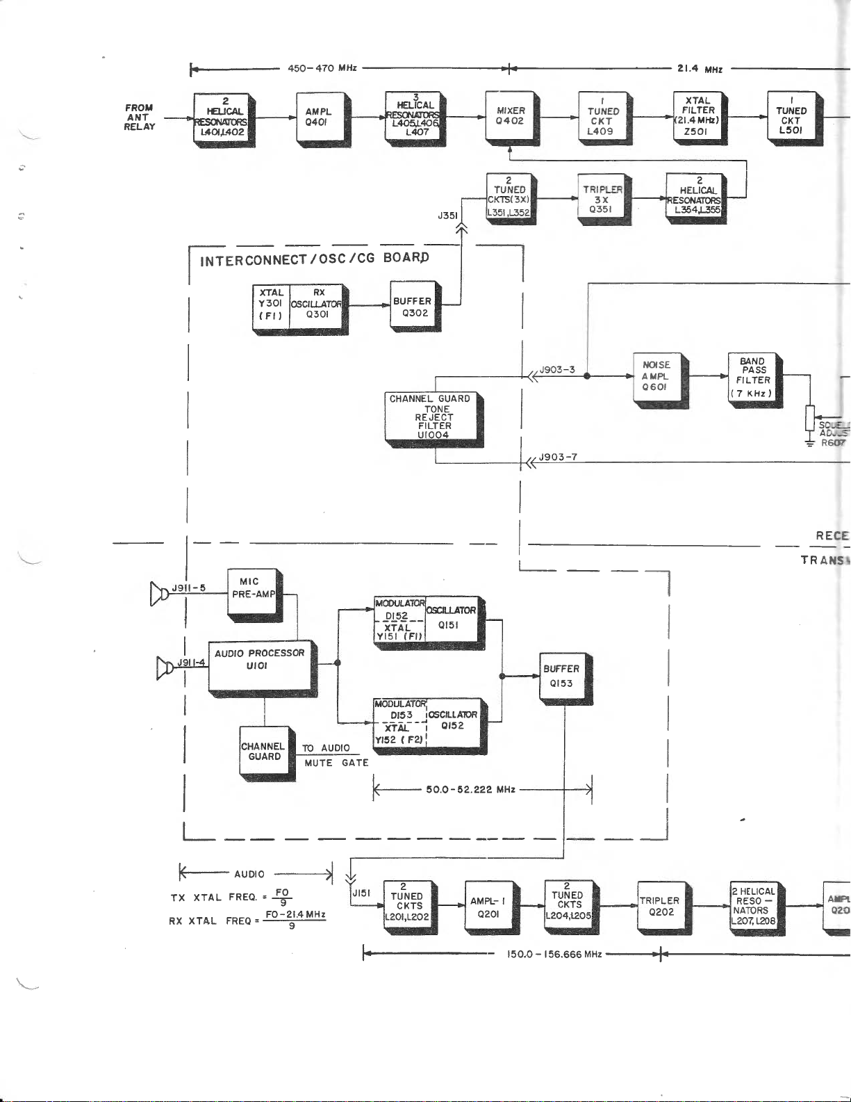
CIRCUIT
The
control
two-frequency
frequency
ter
components
transmitter
U1O1;
Q153,
ampl
control
led,
uses
osci I
exciter
i fier
circuit
transmitters
frequency
operation
band.
integrated
for
increased
consists
1a
tor
stages
Q251
exciter provides
wa t
ts
of
provides
block
transmitter
I\{ICROPHONE
A
associated
modula
rated
diagram
of the
and
PREATIPLIFIER
preamplifier
circuitry)
output
ANALYSIS
TRANS}{I
TTER
utilize
modulated
in
The
solid
circuits
reliability.
of audio
Q151,
through
q2S4
and
e201
Q253,
through
through
approximately
ted
RF
to
power.
radio
receiver.
stage
provided
is
a
exciter
4bO-4TO
the
state
and
processor
Q15t,
and
e287.
150
the
Figure
showing
(e901
crystal
for
transmit-
trtiHz
discrete
The
buffer
e2O4;
power
The
milli-
pA
which
1
is
both
the
and
for
the
pA
a
FF-
45o-47o
MHz
2t.4
uxz
[c,
RCONNECT/OSC
/CG
--l
R ECE
TR
AIiST
I
xrAL
rx
xrAL FRE.
Rx
AUDIO
FREa.
=
-J
E#!I:
=
F3
MUTE GATE
k-
so.o-*z.zzz MHz
-
l5O,O
1 56.566
-
MHz
455 KHr
.--l
LB13
1072
e!!4
osctttaloRz
MIXER/IF
u 50r
AMPL
VOL /SOUELCH HI
FROM CHANNEL
GUARD
A
UDIO
MUTE
GATE
o 605
cERAt'llc
FILTER
(455KHd
2502
AUDIO
AMPL
u6
IF LIM /FM DET/
AUDIO
PRE AMPL
u30?
R 521
AUDIO
LEVEL
0l
;EIVER
TTER
SMI
Z
HELICAT
RESO
-
NATORS
t2t4,L2t5
POWER
0254-
CONTROT
A257
45O -
47O MHz
sxclrEn
e-L+
PwR. AMPL.
RC4240
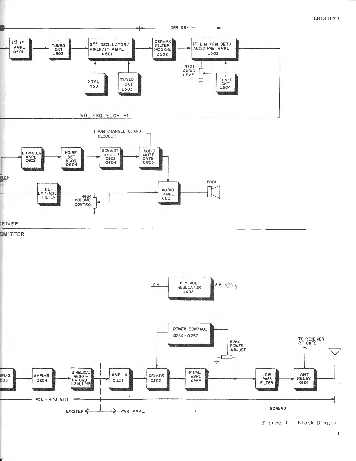
Figurel-BlockDiagram

L8I31072
CIRCUIT
ANALYSIS
standard
built-in
circuit is
coupled
electret
preamplifier.
located
With
this microphone,
througb J911-5
stage. The
through
cessor.
bui
through
AUDIO
pre-emphasis
post
approximateTy
audio
U101B
audio
through
sisting
+4.25V
R908
For
I t-in
J977-4,
PROCESSOR
The
audio
limiter
processor.
and,
The
processor
p9O3-2
of R101,
output
optiona
preampl
4
8.5 Vol
establishes
for
both
provides
of
both
operational
an
operational
Resistors
D101
Diodes
+7.7
R110
cathode
of D102.
D101
permit
and
D102 provide
and
D101
VDC.
and R111
D101
of
The
D102
and
DC
a
the
voltage
biasing.
When
a
magnitude
U1018-7
at
amplifier
Itfhen
exceeds 4
conduct
cycles
reduce
limits
volts
the
such
does
provides
the
audio
volts PP,
on the
providing
the
the audio
PP.
Resistors
comprise
that
R107
curve
trol
pre-emphasis.
attenuated,
the
enhances
and C1O7
below
limiting.
the cut-off
the
Audio
microphone
is
on
ampl i
fied
and C905
1 microphones
i fier,
bypassing
U1O1
n"o".=.o.
with
amplitude
filtering.
24
dB
dB
by
U101A.
t regula
and
applies
to a voltage
R111,
from
the
operating
ground
AC
amplifiers.
R109,
D102
and
Voltage
provides
and
voltage
is 4.25
level
change
divider
input
signal
that
not
exceed 4
a nominal 20
signa
positive
100%
amplifier
amplitude
R105,
audio
the
signal
control
point
As
high
gain
from
the
coupled
microphone
the
board.
preamplifier
The
IOC
MIC
to the
preamplifier
output
to
the audio
audio
MIC PRE
provides
limiting
A
is realized
20
dB
total
is
tor
through
provided
powers
regulated
divider
R110
and R109.
the voltage
reference
amplifiers.
at the
R110,
summing input
R111
limiting
are reverse
divider
+2.6
at
VDC.
network
+b.9
VDC
VDC
at the anode
junction
the
C104
between
network
U101B-6
to
the
amplifier
volts
1
level
at
diodes D101
and
negative
gain
negative
feedback
to
at U1018-Z
R106
and
R10?
pre-emphasis
to noise
pre-emphasis
the
R106
and CLOT
for
high
frequencies
U101
of
is increased.
preamplifier
to
the input
wi.thout
HI
is
coupled
pro-
with
is
coupled
AMp
e901.
audio
and
gain
the
the
+8.5V
con-
The
divider
point
C1O6
and
diodes
for U101B.
biased
R109,
at
the
and C108
U101B-z
for
diode
is of
output
p-p,
the
gain.
dB
U101B-7
and D102
half
1.
This
to b
and ClOz
network
ratio.
con-
frequency
are
or
of
at
of
to
is
of
by
a
a
operational
amplified
through
second
R114,
operational
The
applied
combined
U101A,
per
dB
vide
for
to
with
post
A
R112-R114,
octave
an
additional
a
total
R112-R114
tolerance
a ssure
post
replacements.
The
Q152.
A
output
OSCILLATOR
tempera
is
coupled
compensated
and
TRANSMIT
consi,sting
and
C151
over
a temperature
The
temperature
audio
through
is
MOD
Modulator
frequency
the
audio
Q151,
comprise
rates
RF
osci I
a
the
carrier
lator
operating
lator
is
output
then
coupled
circuitry
boa rd .
The
identical
desired
frequency
frequency
switch
emitter
grounded
selected
Q154.
Q154
is
of
through
oscillator
amplifier
output
Channel
U101A-2.
the
limiter
roll-off.
of
SERVlCE
are 7%
proper
limiter
through
of U1018
R7I2
,
amplifier
Guard
microphone
C10B
6
18
must
dB
dB.
be maintained
opera
filter.
of
the
C110
R104
(CG)
The
filter
and C110
R104
per
resistors.
post
to
transmitter
ture
of
R151,
maintains
applied
ADJ
varactor
at
the
processor.
Y1b1
Colpitts
ninth
compensa
R152,
oscillator
range
compensating
of
to FM
control
D151
varies
audio
and
rate
associated
oscillator
subharmonic
frequency.
is
adjusted
frequency
is
applied
through
L151.
by
to buffer
p1b1
transmitter/receiver
second
to
swi
tch
normally
the
oscillator
the F1
is
S1b1
turned
selected
S151
and
on.
oscillator.
selected
and
Q1b4,
U101B-6.
is
and R11Z
U101A.
tone
CG
tone
audio.
consisting
provides
and C102
octave
This
tion
of
Use
exact
limiter
the
temperature
oscillators
ting
R1b3,
R154,
frequency
-30o to
DC
voltage
modulator
R155
and R1b9.
the
applied
circuitry
which
(50
MHz)
The
the
transmit
assigned
to
The
e153,
to
the
stage
through
channel
on
so
oscillator
tqrning
The
coupled
to
input
is
then
pro-
roll-off
to
the
filter
Q151
network
D1b1
+60.C.
and
DIS2
transmit
from
g.ne:
oi
the
oscil-
and
exciter
(Tx/Rx)
is
The
Tx
Common
that
the
is
the
a
is
of
12
CIRCUIT
ANALYSIS
L8r31072
SERV I CE
Tbe
channel
factory
circui
to
posi
t
be checked
tion
consists
Groundirg
J911-6
each
turnecl
transmit
and then
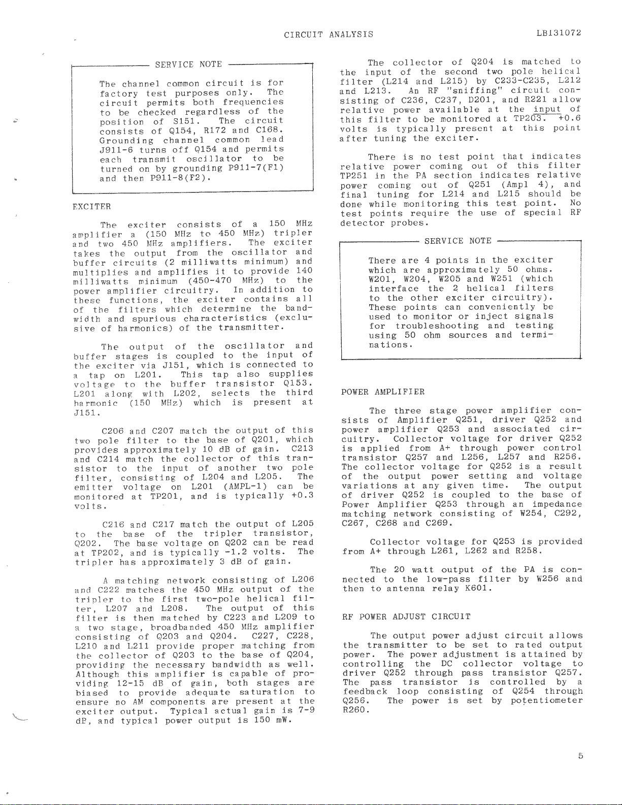
EXCITER
The exciter
the
a
450
output
amplifier
two
and
takes
buffer circuits
multiplies
and
milliwatts
power
these
of
width
sive
buffer
the
a
amplifier
functions,
filters
the
and spurious
harmonics)
of
The
output
stages
exciter
tap on
L2O1.
voltage to
L201
harmonic
J151.
provides
along
C2O6
pole
two
C2l4 match
and
sistor
(150
and
filter to the
approximately
to the
filter, consisting
emitter
voltage on
monitored at
vcl
ts.
C216 and
the base
to
Q202.
at'lP2O2,
tripler
The
and
has
A matching
C222 matches the
and
tripler
ter,
filter
a two
to the
L2O7
is
tben
stage, broadbanded
consisting
L210
and
L211
the collector
providing
the necessary
common
test
PurPoses
permits
regardless
S151.
of
of
Q154,
channel
turns
off
oscillator
grounding
by
on
P911-8(F2
consists
(150
\llIz
amplifiers.
I{Hz
from
(2
milliwatts
amplifies
minimum
(45O-47O
circuitry.
the
whicb
characteristics
of
of the
is coupled
J151, which
via
This tap also
the buffer
with
L2O2,
\!lHz) rvhich
C2O7 natch
the collector
input of
of
Tp201,
C2I7 match
the
of
voltage on
base
is t1'pically -1.2
approximately
network
first
L2O8.
and
matched
of
of
and
Q203
provide
Q203
Although this amplifier
viding
hiased
ensure
exciter
12-I5
to
no
output.
dB, and typical
dB of
provide
AM
components
power
adequate
Typical actual
circuit
is
onlY.
frequencies
both
of
The
circuit
C168.
and
Rt72
Q154
common
and
P911-7(F1)
lead
Permits
to
).
a
of
45O MHz)
to
The
the
1t to
minimum)
provide
I 1a tor
osci
I{Hz)
In
addition
exciter
determine
the
contains
the
transmitter'
1a tor
I
osci
to the
is connected
transistor
selects
the
base
10
dB
present
is
output
of
Q201'
gain.
of
of
the
this
another
L2O4 and
LzOl
is typically
and
(AMPL-1)
L205.
the output
Q2O2
dB of
transistor'
ean
vo1ts.
tripler
3
consisting
450 MHz output
two-po1e
The
by
Q204
proper
to the
helical
output
C223 and
450
[4Hz amplifier
. C227
matching
base
bandwidth
is capable
gain,
both
stages
saturation
present
are
gain
150 mW.
output
is
for
The
the
be
1.50 llHz
tripler
exciter
to
band-
(exclu-
input
supplies
Q153.
third
thls
of
which
C273
tran-
pole
two
can
+0.3
L205
of
read
be
gain.
L206
of
of the
fi1-
of this
L209
C228
,
from
of
Q2O4,
as we11.
pro-
of
at
is
and
and
140
the
to
aIl
and
of
to
aL
The
be
The
are
the
7-9
to
to
The collector
input of the
the
filter
and
sisting
relative
this
volts
after
(L214
L213.
An RF
of C236,
power
filter
to be
is typically
tuning
and
the exciter.
There is no test
rela tive
TP251 in the
power
final
done while
test
detector
power
coming
tuning
monitoring
points
There are
which
W201,
require
probes.
are approximatelY
W2O4, W205 and
interface
to the
These
used
other exciter
points
monitor or
to
PA
out
for
SERVICE
4
the
for troubleshooting
50
using
ohm
nations.
POWER AMPLIFIER
The
three
sists of
power
cuitry.
is applied
transistor
The
colleetor
the output
of
variations at any
driver
of
Power Amplifier
Amplifier
ifier
ampl
Collector
q252
from
q257
voltage for
matching network consisting
,
C268
C267
Collector
A+
frorn
through
The 20
nected to
to antenna
then
POWER ADJUST
RF
The
'
the
power.
control
driver
The
output
transmitter to be
The
ling the
Q252
pass
C269.
and
voltage for
watt
1ow-pass filter by
the
power
through
tra nsistor
feedback loop consisting
power
Q256.
R260.
The
of
Q204
second
L215)
two
C233-C235,
by
"sniffing"
C237,
available
D2OI,
monitored
at
at
present
point
of this
coming
sect.ion
out
indicates
of
Q251
L214 and
L215
this test
use
the
points
2
in the
W251
helica
circuitrY).
can conveniently
inject signals
and testing
sources
stage
Q251,
Q253
voltage
and
power
driver
associated cir-
and
for driver
A+ through
L256,
and
power
given
is coupled
Q253
L267,
through
L262
L257
Q252
setLing and
time.
to the base of
Q253
and
output of the
relay
CIRCUIT
power
K601.
adjust circuit al1ows
set to rated output
adjustment
DC
lector voltage to
col
pass
transistor
i s control
of
is set by
is matched
pole
helical
circuiL
and
R221 allow
input
the
TP203.
point
thj"s
at
indicates
that
fil ter
relative
(Amp1 4)
,
should
point. No
of special
exciter
50
ohrns.
(which
I fi1 ters
be
termi-
amplifier
power
and
q252
control
R256.
is a result
voltage
The
output
an impedance
provided
PA
is con-
W256 and
I
ed by a
through
C292,
q257.
of W254,
is
R258.
is
attained by
Q254
potenLiometer
to
L272
con-
of
+0'6
and
be
RF
con-
and
Q252

L8r31072
CIRCUIT
ANALYSIS
A
D252
change
output
goes
change
causing
accordingly.
power
more
conduction which
age.
Q254
increases
duction.
to the ba se of
Cecreases
Q256
voltage
base
resulting
lowers
q252,
proport
the col
tberetry
ion to
a1ly sensed by
The
superheterodyne
in output
the
base
increases, the
positlve,
causing
lowers
controls
Q255,
conduction,
This
raises the
Q256.
proportionally,
pass
of
transistor
decrease in conduction
lector voltage of
lowering the output
the excessive
the base circuit
RECE I
receivers are dual
FI\'I
receivers designed
one-frequency operation
frequency
used
audio
supply.
'The
quencies
for
PA
all
range. A
receiver stages except
IC,
whjch operates from the
regulated
receiver has intermediate fre-
21.4
of
liHz
and
power
voltage of
For example,
its col
Q255
Tbe
VER
in
455
is
sensed
q254
if the
base of
it to
increase
lector volt-
therefore
as
decreases
voltage applied
conduction
lowering
Q257.
of
driver
power
power
of
ori
Q254.
conversion,
42O-572 \lHz
Ihe
8.5 volts
for the
kHz. Adjacent
by
to
Q254
Q254
con-
of
the
The
Q257
in
gin-
for
is
A+
channel selectivity is obtained by using
two band-pass
fi I
ter and a
Al1
the
transmit
osci
receiver
455
of the receiver
1 1a
ter/receiver
consists of:
filters:
kHz
tor
is
21.4 MHz
a
ceramic
fi 1 ter.
circuitry
mounted on the
(Tx/Rx)
board.
crystal
except
The
frequency
crystal operateci at one ninth
required injeetion frequency.
variable
connected
capability.
is control led by
capacitor
in
series to
The
D301, L301
provide
compensation
third mode
a
of
Voltage-
Y301
and
compensati-on
voltage used
the
are
to control the transmitter oscillators is
applied to
L301
is
frequency. R301
to insure
of the
C304 to the
output
crystal.
The
of
two tuned
Tx/Rx
board.
the third barmonic
quency
Q351.
coupled
through helical resonators L354
L354
and
frequency
nultiple
The
multiplier
The
meter reading
ly 0.8 VDC. The
oscillator/multiplier
to
the mixer
meter
1
tor
1ST
reading
volts
Probe.
I{IXER
D301
maintain
to
stability.
adjustable to set the oscillator
is in
parallel
with
operation on the third overtone
output of
emitter of buffer
is coupled through
Q302
circuits
L351
Q301
(L351
and
is
coupled through
Q302.
L352)
and
L352
are tuned to
P301
on the
of the oscillator fre-
which is
The
to the source input
applied to the base
output of tripler
of
A351
mixer
and
L355
are
tuned to the operating
minus
of the
DC
27.4
MHz
which
is
crystal frequency.
leve1
of the
osci
chain can be monitored
at
RF
point
this
frequency
is
the ninth
1 Iator
TP351.
at
typical-
from
chain and input
can be measured
at
measured
as
TP401
is
using the Rx RF Detec-
TP401.
at
typically
0.5
Y301
The
Q402
L355.
the
level
The
to
of
is
/
to
Receiver
21
.4 MiHz
1st
and
455
kHz
Detector
Audio
Squel
RECE]VER FFONT ENI)
An RF
conpled
helical
t'ase of
Q401
through
resonators
RF
is
coupled
resonators
gate
of
1st
lectivity is
resona tors.
OSCILLATOR
Q301
make
up
PA
ch Ci rcui t ry
signa 1 from
amplifier
consisting
Mixer
provided
IVIULTIPLIER
&
Y301
,
Colpitts-oscillator.
a
Front End
1st
IF
2nd
Oscillators
2nd
IF
Circuitry
antenna
(L401
Q401.
through
Q402.
nd
a
a ssocia
circuitry
circuitry
the antenna is
and
K601
L4A2)
relay
The
three
of
by
more
L4O5-L4O7
The
front
the
five helical
ted ci
FM
with
and
to the
output of
helical
to the
end
rcui
The
two
se-
try
The 1st
active
high
device. The FET
input
an output
products).
tion
In
end
of the
the
helical
mixer. Injection
multiplier
of
the
output
Q402
(L409
2501.
provides
IF
is
work
IST
I{OSFET.
plied
mixer. The 21.4
signal
through
and
The
highly-selective
the
selectivity.
coupled
L501
2ND
&
1st
IF Amplifier
The
Gate 1
to
ampli-fied
The
biasing
determines
mixer
impedance,
relatively
mixer
filter
stages is
is
coupled frorn
an impedance
C410-C413
first
The
through
to
IF
1st
the
DETECTOR
&
crystal
of the
signal is
Gate
on
gain
the
uses
a
high
(Q402)
FET
mixer
provides
power gain
free of intermodula-
stage, RF
is
applied
from
to the
the front
voltage
applied to
MHz
the source
mixer
the
matching
to crysta 1
)
crystal
portion
output
impedance-matching
IF
of
amplifier.
STAGES
e501
filter
the receiver
of tLre
is
dual-gate
output
amplifier,
taken from
2
and the
of the
the
drain
stage. The
as the
and
gate
from
the
1st
lF
drain of
network
filter
filter
filter
net-
is
ap-
and
the
drain.
load
a
o

CIRCUIT ANALYSIS
L8r31072
amplifier
gain.
IF
provides
through an
(L502)
the
of the
that
input of
U501
and associated
2nd
amplifier.
Y501,
is
20
"945
2nd IF
side
for those
and the oscillator
lllHz
(standard),
injection with
radios
The
impedance
matches
IC U501.
oscillator,
The
f or lovr side
approximately
output
the amplifier
crystal
or
(Structured Option
determined to
on a tweet frequency.
mixed
with
21.4 MHz input.
the
of the mixer is lirni.ted
L503 is
quency.
ceramic
kHz
tuned
The
output
filter
selectivity, and applied
for the
of
Z5O2
455
U501 is
wlnich
Point TP501 is used in a
ver,
and can be
u501.
U502
and associated
455
of a
detector
is the
Level
kHz
and an audio
quadrature
potentiometer
audio output level
used
to
limiter, a
detector coil.
R521 is used to set the
to the audio
of
Q501
matching
circuitry
mixer
20
is coupled
output
consists
and
of
dP
network
to
2nd IF
for the oscillator
in
ject
operates
ion of the
aI
21.855 MHz for high
be operating
FT)
This
by
D501
kHz
frequency
The output
2nd lF
coupled
provi.des
U502. Test
to
ligning the
check the
and
output of
D502.
fre-
through
455
the
recei-
is
circuitry consists
quadrature
preampl
i fier.
type
L504
Audio
FM
amplifier.
1oad.
The
output
is
noise
7 k{z.
The
noi
Squelch
which
Q602
se output i s coupled through
control
R607 to expander ampllfier
improves
the level discrirnina-
tion characteristics of the
output of
voltage
This
and operates as
circui t has a high
Fol
Q602
doubler
lowing
Schmidt trigger
trigger
and a
IIUTE
provides
1-defined
we1
gate
Q605
Wi
th no RF
detected noise
output
This
volts
This
turns on
causes
pin
to
voltage
is
applied to a
circuit
average value
an
vol
the
(Q603-Q604
tage doubler
the necessa ry
output signa I for Rx
signa 1
Q605
2
a t the
Q603,
to turn on,
of audio
turning
turns off U601
(D603
source impedance
vol
receiver.
When
noise
drive
Q603
turned
This
at the output
to
and al1ows
oD,
turns on U601
an
e603
Rx
RF
signa I is
is
removed.
Q604
IVIUTE
of
Q601
to turn on.
gate
so
that audio i-s
at the speaker.
in
a band around
circuit.
and
rectifier.
. The
)
hysteresis
present,
tage
off
applying
amplifier
and mutes
received
decreases
This
turns
With
Q605
turns
The
passive
D604).
is a
Schmidt
the
doubler
Q604.
+1.
U601.
the
the
,
and
off
Q604
of f
heard
.
AUDIO
Audio
tone reject filter through
to the de-emphasis
The
network
Cont
speaker at
three
R637,
fiers
vide the higb
above
DC
(Q605)
These
squelch
the
through
Squel
noise components
detector
AND
SQUELCH CIRCUITS
Audio
is
applieC
to the
Channel Guard
P903-3
network through
audio
passes
(R633,
rol R634.
Audio
arnplifier
the
watts).
R638
and
closed loop
6
kHz.
The
audio amplifier can be
voltage
from the
through the de-emphasis
C608
C609
and
IC
)
U601 drives the
desired audio level
The
C611
plain.
audio
feedback
determines
loop containing
R636
and
frequency
receiver
the ampli-
muted
mute
which uses different logic inputs.
inputs are
signal.
Channel Guard
P903-4.
ch
Tbe
squelch
output.
8.5 V Tx,
The Rx
MONITOR, or
MUTE function from
circuit which
circui t operates
contained
The
output of
in the
is applied
applied to frequency selective
arnplifier
(L601,
Q601
R604
that has a
and C6O2) as the col
resonant circuit
and back
P9O3-7.
Volume
to
(up
pro-
C613
rol 1-off
by a
gate
on the
U502
noise
lector
to
FM
is
The
R607 in
fier
Q602.
Pressing
the front
disable
the base
squelch
the base
of the
the Channel Guard. It
of
sensitivity is
circuj.t of
in
the
radio opens
and
Q601
expander
MONITOB
disables
adjusted
ampli-
pushbutton
the Rx
also
the
MUTE
grounds
squelch
by
on
to
function.
CHANNEL GUARD
Channel
encoder/decoder
quencies
The
encoder
to
the transmitter. The
in
conjunction
all
calls that
proper
Channel Guard
The
of discrete
a
disable, PTT
switch; four
modules
Encode
consisting
Module
Selective
Versatone
U1004
in
For
nel Gua
rd
troubleshooting
References
in
the fol lowi-ng
Gua
rd
is
for
in
the
provides
operation
71.9 Hz
tone-coded
with the receiver
are not
frequency.
Channel
Guard
components for
switch,
thick-film
U1002,
Frequency
Decode
of
Amplifier (FSSA)
Network
ZIOOI
the tone reject
f uncti-ona
a
Encoder/Decoder
I di.agram
procedures.
to
symbol numbers
text are found
a continuous
on
210.7
to
decoder
tone fre-
Hz
modulation
operates
to inhlbit
tone
coded
circui try
wlth the
consists
the
and receiver
integrated
Module
U1003, plug-in
Swi.tchable
and monolytic
filter.
of
the
refer
,
mentioned
tone
range.
Encode
mute
circuit
U1001,
Chan-
to
the
on the
IC
Ltsr31072
CIRCUIT ANALYSIS
Schema tic
Diagram,
Outline
Diagram
and
Parts List.
FSSA
Frequency
(FSSA)
fier
bandpass filter for
Switchable Selective
U1003
frequency range.
is a highly stable
71.9 Hz
the
The selectivity of
2I4.7 Hz
to
Ampli-
active
the
filter is shifted across the bandpass
frequency
Networks
The
the tone
determjned by the
FSSA
the
precision
is
a
ENCODE
V/hen PTT
Gua
ne I
range
in
the
gain
by swi tching
fi I ter
of the
frequercy.
Tone
circuit.
Versatone Network
resistor network.
t
swi
rd
encode t one i s
ch i.
coupling the output of
U1003
inverting amplifier
circuit.
from U1003
inverting
back to its input
circuit and a limiter
The
output of the
to
the
amplifier at
rcui t
ci
FSSA
is a
The Tone Frequency
Network
s
opera t ed
FSSA
bandpass filter
through a
input
FSSA is
U1002-9.
Versatone
.
function of
connected
the
,
genera
of the
21001
Cha n*
by
ted
phase
coupled
phase
is
in
the output
peak
to
the
it to
coupled
peak.
to
The
Pin 12
proper
pass.
to
output from the limiter is
of
to an amplifier
amplifier
put
of a threshold detector
In
at
the
er in U1001
quency,
mutes
mode,
MUTE lead
Q1005
the
Q1006
and muting
Audio
tone reject
is an
active
associated
7O
while
back
tered
210.7
to
passing
to the recei'rer
VOL/SQ
STANDARD TONE
U1001-13
at
FSSA U1003.
frequency,
The
U1001-3.
circuit.
U1001-4
mute mode,
detects the
turns
receiver
is
operating,
from VOL/SQ
filter.
filter
circuitry.
Hz
are rejected
all other
HI
).
55
the
Lo
Since
FSSA
millivolts
the tone is
will a1low
output of the
U1001-3
is
coupled to the in-
when
Channel
Q1006
audio.
is
The
output
U1001-6.
at
the tone decod-
Guard
off.
In
the squelch
grounding
receiver
the
HI
is
The
consisting
A11 frequencies
applied to the
tone reject
of
by the fj.Iter,
audio frequencies
audio
FREQUENCIES
circuits
(Hz)
coupled
FSSA
is
the input
of the
fre-
This
un-
the Rx
audio.
filter
U1004
and
from
(fil-
An
amplifier
of the tone frequency
output
circuit
input
put
the
to
of the
is
of the limiter
A
limiting network
coupled from U7402-4
The
limiter
(U1003-12)
FSSA
peak.
provides
at the output.
phase
inverting
coupled from
circuit at
at
circuit
encode switch. Keying
+5.4
applies
the
ci rcui t osci I 1a
cy is
determined
nected in
The
is taken
tone
output
adjustment
Volts
to
t i ng. Tbe
by the
FSSA
the
circuit.
tone output
U1002-7
from
ampl
81010
i
fier
to
UlO02-2.
of
the encoder
and
Q1002
the audio
the transmi tter/receiver
DECODE
Aud
i
contains
pin
to
U1001
stage,
ter
The
U1001-15
is
the input
o from
the
1
of
is
the input
pass
low
attenuates frequencies
output
is
Vol
ume/Squel
correct
Decode
Module
filter. The
of
the 1ow
applied
to
of a limiter
frequency
of an
U1001-14.
phase
180o
amplifier
U1002-6
to the
U1002-5.
sets the tone
to
53
the input of
millivolts
is
also
used
the transmitter
This
starts
tone frequen-
tone
network
circuit
coupled
and
through
modula
processor
board.
ch high
is
coupled
U1001. Pin
act ive,
pass
low
21O.7
over
pass
fi lter
U1001-14
circui t, limiting
shift
The
out-
peak
as an
con-
t ion
on
tha t
1
of
three
fil-
Hz.
at
77.9
7
4.4
77
.O
79
.7
82.5
85.4
Encode
Disable
The
been
a nce
This
Guard
the
ter
checks
from
The
Q1003
and
circuit,
VDC)
is
at
the
plt"!gO
DISABLE)
rear
voltage
turning
88
.5
91
.5
94.8
97.4
100
.0
103.5
SERVICE
Encode
incorporated
id
a
for
circuit
encode
serviceman
distortion
without
the
radio.
Encode
a
Di.sabIe
Q1004.
positive
applj.ed
of
by
to
is
on
the
temporarily
p910-11
applied
both
707.2
110.9
114.8
118.8
123.0
t27 .3
Disable
as a maj-nten-
the
disables
cireuit
to make
and modulation
removing
circuit
To
disabte
voltage (+8.b
to Molex
radio.
jumperins
(A+).
to
the
Q1003
131.8
136.5
141
146.2
151
756.7
203.5
270.7
.4
162
I67
.3
t73
179
186
192
circuit has
servi
ceman
the Channel
and
allows
transrnit-
the
cover
consists
the
connector
This
is
pgto-9
positlve
Thls
base
of
and
2
o
8
o
2
8
.
encode
to
p910-b
accom-
(CG
e1003,
e1004.
of
14

CIRCUIT
ANALYSIS
LBIU1072
turned
\{hen
base of
the
off.
for
Output
preventing
With
Q1001
encocler
the
Stage transistor Q1002
any
When usinpr
cuit,
f
rom t
do
he opt
present)
on the
hookswitch
tion.
place
not
desk
This
microphone
will
ground,
the
to
radio through
the
rea r system
Both
protection
ity
ground
equipment.
The
lnputs
lead
battery
connector
ground
which
dently
through
will open
connected
oD,
Q1004
PTT Switch
off,
IC U1002
output.
tone
CAUTION
Encode
the
remove
rot
i ona
place
or
In station
CG
the
short
the
resulting
POWER
DISTRIBUTION
voltage
J910-1 and
connector
connected
are
diodes
is coupled
is connected
and
fusable
a
if the
A+
to
app1ies
+B'5
Q1001,
operating
the
and
Encode
is
Disable
microPhone
the
hookswi
t
monitor
the
in the
"uP"
aPPlications,
Switch
MON
[{ON
in
supply
possible damage
in
Position.
voltage
(A+)
J910-11
the
to
reverse
to
D901
and
through
to chassis
printed
ground
(see
wire
Figure
VDC to
forcing
voltage
Tone
removed,
r-
ci
(
t ch
i f
switch
posi-
do
the
on
to
connects
at the
IOC
boa
polar-
D9O2.
same
the
ring
wi
is acci-
2).
it
to
rd.
The
run
One battery
IOC boa
the
capacitor
stages.
P903-6
One
branch
through
one
and
switch
POWER On/Off switch controls
in
The other
to the
for the audio
RC-rippte
an
of the sections
S602.
input
rd through a
FL9OT
main board
The
voltage regulator
output
selected
Receiver
selection
either the
Tx
antenna
volt
relay
microphone,
sor
is fixed at
resistor
Schematic
instructions.
Regulated
8.5 volts i-s switched to
receiver or the Lransmitter
indica tor by the antenna
relay is also
regulated supply.
is
operated
by the
completing the
The
squelch circuit,
and
parls
of the
supplied directly
goes
the lransmitter
to
input
for two
amplifier
flller
(R642
of
other
U602.
section
The
8.5 volts
R640.
Refer
Diagram for resistor
powered
The
PTT
path
the audio
IF
amplifler
from the continuous
volt supply.
The receiver front-end, the
oscillator,
second
oscillator are supplied
Rx. The
exciter
are supplied from
21.4 MHz
the
transmitter
IF
stages and
oscillator and the
8.5
directly
from
feed-through
feeds
through
functions'
passes
C619)
and
POWER On/Off
of lhe
A+
the
regulator
means
by
relay
by
to
'
the
the
and
The
8.5
non-latching
switch on the
A-.
to
proces-
U502
are
8.5
receiver
the
8.5 V
from
V
Tx.
PA
to
ol
EATTERY
tcNrTtor
(OPTIOMLI
BATTERY
MIC ROPHONE
M IC ROPHONE
INTERCONNECT/OSC
(+}
5w
(-}
PTT
/ CG BOARD
PWR ON INOICATOR
M lC PRE
AUDIO PROCESSOR
I
TX
OSC CKTS
ON
A[4P
TRANSMIT/RECEIVE
RECEIVER
TRANSMITTER
CKTS
TRANSMIT INOICAIOR
EOARD
CKTS
Figure
2
Power Distribution
-
I

LBr37072
MAINTENANCE
PREVENTIVB I{A
To
from interrrlpting
electrlcal
checks as listed in
CONNECTIONS
should
tions to
INTENANCE
insure- bigh
parts
Ground
-
periodically
be
the
power
operating efficiency
system
at regular intervals,
the table of
source
operation. When ground
tery, the
checked for low
age drops
ELECTPTCAL
erator
economical
tery loses
week
tery
I4ECHANICAL
shock a nd vi bra
to mal<e
ANTENNA
clean
should
signal
connection
impedance. A
and alternator
sYsrEM
periodically
operating
water rapidly. usage
is acceptable
will
often
cause excessive noise
INSPECTION
t i
sure that
The
-
and free
become
antenna,
from
coated
will result.
check
-
to
for
on
,
nothing
dirt
or
operations,
routine
checks
to
and
This
Maintenance
MAINTENANCE CHECKS
Checks.
connections and connections
checked for tightness.
Loose
will cause excessive voltage
connections
from the battery
high
noise
voltage
the
keep
the
limits. over-voltage
batteries in
Since
-
check
antenna
for 1
is
working
or
corrosion.
mobile
poorly
are not made
to
impedance may
problems.
regulator
electrical
of 1 or
continuous
or
units
p1ugs,
oose
I oose
base
and
grounded,
vehicle
system
is
indicated
2
ounces
operation.
faulty
are
subject
nuts,
.
all
contacts
If
the antennas
loss
of radiation
prevent
mechanical
should
preventive
to
the voltage
poor
or
drops
directly
chassis
cause
and
excessive
alternator
within
of
when the
water
operation.
to constant
screws
should
or
made
be
maintenance
source
connec-
faulty
and
to the
must
bat-
be
volt-
gen-
or
safe and
bat-
per
ce1l
A
weak bal-
parts
and
kept
be
its
base
and
a weak
and
electrical
fail"ures
of all mechanical
should
per
o
Mon
x
x
X
include
lNTERVAL
t hs
Requi
and
the
AS
red
X
ALIGNMENT
checked
Refer
for
typica
FREQUENCY
quired
put
into
after.
DI
SA SS EI4BLY
The
-
periodically,
to
the applicable
transmitter
I voltage
CHECK
hy FCC.
Check
-
Normally,
operation,
To
service
receiver (Tx-Rx)
tvzo
screws
cover
Then
under
at
the rear
sl ide
tbe
control panel
To
service
the
two
radio
the
panel
screws
and
edge
and
sl
of the
lift
and
the alignment
ALIGNI{ENT
readings.
transmitter
these
after
the first
the
board,
securing
the
cover
edge
and
lift
IOC
the
at the
ide
the
.
off
receiver
and
ehecks
transmi
loosen
the
of the
out
of the
off.
board,
rear
cover
front
meter
PROCEDURE
"touched
frequency
are made
six
months
tler/
the
bottom
radio.
from
front
loosen
of
the
out from
control
readings
up"
and
and deviation
and
when necessary.
troubleshooting
when
the
once
should
as re-
unit
year
a
Be
careful
top
leads
boa rd .
To
remove
Remove
covers.
Remove
the
frame
panel.
be
sheet
is first
there-
are
when
as
connected
cover
the Tx-Rx
the
the
four
front panel
a nd
removi.ng
the
speaker
board:
top
screws
remove
to
and
to
the
x
x
the
the
bottom
securing
,,H,r
the
front
10

I NTENANCE
I{A
LBr:i1072
Remove the
ing the
Unsolder
and
screws.
Remove the
5.
RF shield.
the
remove
transistor
Turn the radio
the
copper
spacer
screw
hex
Driver transistor
Remove the
7.
Tx-Rx board
the
up
lift
erconnec
i nt
the
To remove
t i-frequency
mul
Remove tbe
t
In multi-frequency
move the
RF
the
J.
Remove the
shield.
the board
the board
interconrection
eight
screws
antenna
trto
the
screws
two
Q253.
and
over
Post,
from
washer
the
Q252.
9 sc rews
and
board
i
ons
t
the
off
.
ns
Pi
interconnect/
rd
boa
toP cover.
units,
five screws
12
screws
carefullY
and
up to
disconnect
pins.
secur-
connector
retaining
PA
the
in
remove
and
of
stud
securi
ng
carefullY
of the
;
t€-
securing
securing
lift
the
printed
part
circuit
the matching
of
included in the base
runs.
Tri-m
4.
the
new
required) lo
the removed transi
1et Ler
rrcrr
transistor a
lector
col
t ransistor lead
Apply
between
the
coa t of si
a
the mounting
spacer
the insulator
mounting surfaces of
the
the heat sink and
the spacer.
in the mounting
leads as shown
Diagrarn. Then
the transistor
board
translstor
the lead length
on the top
lso indicates the
(see
identifica tion
and to both sides
of
Place
hold the
runs
network
and
stor.
Figure
1 icon
surfaces of
and between
Q252
on both ends of
the transistor
hole.
on
the
and replace the
transistor mounting hardware,
using modera te
Newton
pounds)
1.0
screw
be
transistor
too
used.
meters
for M2.5 screw size and
(8
Nm
inch
post.
used for this adjustment
little
damage can result
or
torque of
(Nm)
pounds)
A torque
much
too
or
for the hex
wrench
because
collecLor
leads
(if
of
The
of the
3
for
.
)
grea
se
of
and
Q253
Align
the
Outline
of
body
0.6
6
inch
must
since
if
torque 1s
is
I]RIVER
The
tors used
-AND
stud
TRANSISTOR
PA
mounted
in the transmitter
Beryllium Oxide, a
If
the ceramic
is opened, crushed,
tion
abraded, the
i f inha
led .
transistors
To
replace
Q253:
1 . Rernove
2. Unsolder
50
watt
scribe or
the lead away
circuit
cool s.
Lift
out the transistor,
move the old
printed
sol deri
PULLTo.
taken
REPLACEMENT
WARNING
Power
RF
TOXIC
other
or
may
dust
Use
care
one
tYPe.
boa
lead at a
of this
PA RF transistors
Tx/Rx
soldering
substance.
encaPsula-
be
in
.
rd
iron.
X-actroo
from the
board
until
solder
circuit
ng tool
Special
prevent
to
board with a
such a s a
care
damage
Transis-
contain
broken
hazardous
rePlacing
Q252
time with
knife to
Printed
the solder
and
from
should
to the
or
Use
hold
SOLDA
and
re-
the
de-
be
b.
Solder
the
circuit
inner
edge of
solder the
transistor
care
that
not to use excessive heat
causes the
runs to Iift up
Check
for shorts and solder
leads to the
pattern.
Start
mounting
remaining length of
lead
to the board.
printed
from
printed
al the
hold and
Use
wire board
the board.
bridges.
CAUTION
Failure
leads as
the
could
may
a
a
7.
REMOVING
Removing ICrs
to solder the transistor
directed may result
generation
damage the transistor
cause
Replace
low
Tx/Rx
RF
of
power
output.
board and reassemble
radio.
!
}C
S
(and
loops
that
a1I other
in
or
soldered-in components) can be easily
accomplished by using a de-soldering
such as a
remove an
SOLDA PULLTo
IC,
heat each lead separately
or equivalent.
tool
To
on
the solder side and remove the old solder
with the de-soldering tool.
11

L8r31072
MAINTENANCE
o252
NARROW
LEAD
IS COLLECTOR
Figure
An a I ternate
special soldering
pins
simul taneously.
TEST AND TROUBLESHOOTING PROCEDURES
Maintenance of radio
use of the
servicing
Troubleshooting Charts
techniques
method
tip that
unique to this
is to
heats ali
is facilitated by
The Troubleshoot ing Chart is designed to
you
lead
or circuit.
provided
reference
rapidly to the
Typical
on the
when
Schematie
troubleshooting.
defective component
voltage
Diagram
3
- Q251
use a
of the
and
radio.
readings are
your
for
NARROW
LEAD
IS COLLECTOR
M2.
5 XB---=-
REW
SC
Lead Identification
signals
S
and
connectors on the
To
isolate a
determine loading
circuits, ete.
(plastic
or
appropriate
nector
paths
SQ
II{UTE
TEST POINTS
to
create an
that may be
HI,
filtered
nd SPKR HI
a
,
voltages
IOC
board.
signal or voltage
effects, loca
carefully insert
wand,
pins
toothpick)
of
the related
open circuit. Signals
isolated
volume
.
squelch
025 r
RC4?75
pass
include:
through
path
te short
an insulat-
between
Molex
Volume
HI, PTT,
the
to
the
con-
Rx
.t
I
'I
Troubleshooting
for most major
Transmi
the
tter/Receiver section of the
prob'lems
charts are
that
radio.
SFRVIClNG TECHNIQUES
The
high
modular radio lends itself
jsolation
and signal
Tp201
'TP2O2
TP203
Al{pL 1
TRIPLER
AMPL 3
TP251 AI{PL 4
12
cl.ensi ty
rpalfunctions
of
paths.
TRANSI',f
(Q201)
(Q202)
(Q204)
(Q251
plug-in
A
ITTER
Emitter Voltage
Base
Relative
Rela t i ve Out
)
might arise in
provided
desigr of the
well to
in the
rapid
voltage
majority of the
Voltage
Output
put
RF
section
poses
and
injection
An
RF
signal
monitor
Seven
eritical
operation.
They
TP351
TP401
TP501
Detector probes
are
available
to monitor
TP401
at
and the
probe
also is
the transmitter
test
circuit
points
locations
are as follows:
RECEIVER
Tripler
Receiver
455
kHz
Output
1st
oscitlator
IF
for
for alignment
the recei-ver
pur-
the lst receiver
2nd IF
at TP501.
available
frequency.
provided
are
to monitor
-
Q351
injection
to
al
MAINTENANCE LB131,O72
CAUT ION
iir
ri
il'
Before
bench
To
the
bench testing
power
protect
following input
supply.
the transmitter
radio
the
power
voltages must
Transrnitter unkeyed:
Transmitter
Transmitter
These voltages
take the
non-optimum load
voltage drop of
encountered in
Routine
transmitter
for loads
for transient
Many
commonly used bench
are
is for
practice,
0
to 6 amperes:
of
peaks
regulation and transient
keyed
keyed
specified
standard
"worst
the actual
tests should
short duration.
of
power
voltage suppression. Bench
force" regulation and filtering
automotive storage
battery.
be sure of the output voltage
output transistors from
not be exceeded:
20
Volts
(50
(no
at
case"
Input
resistive load):
ohm
load or non-resistive, load):
the normal vehicle
cables into
account.
conditions. For
limit
be
wiIl approach the
performed
voltages
battery
EIA
at
Standard
must not
antenna mismatches 1ikely
supplies cannot meet
may be usable
when operated in
characteristlcs
possible
18
Volts
terminals
The
voltage limits
18
instant
15.5
VoIt
Volts
of the radio
figure.
Test Voltages
exceed the limits
these requirements
supplies
which
parallel
of
destructi-on,
shown for
(13
shown
for
employ
with a
12 Volt
your
and
a
to be
VDC
even
load
"brute
r,t .
'/ui,:
GENEFAL
WORLo
ELECTRIC
COMPANY.
HEAOOUARTERS.
MOBILE
COMMUNICATIONS
LYNCHBURG. VIRGINIA 24502
DIVISION
U.S.A.
fradema.k ol
General
E lectric CompanV
PrintedinUSA.
U.S.A
GEN
ERA L@ ELEOTRIC
13

LBI3 LO72
A,*o'r,,rru
It3 FLAT
t PTACES
XASHER
,A Arpzeoszz
--COIIBI
NATION
II;IITPLATE
A
ArT
1
SCRIH
A
fsrf.l
3 '2.
'A'
A B
AST
Corr
r1t7ffi.7P2
l1t7mJ2f5
il
LocI
PLICES
I
,A rwoocltrrto
'"tttix0.5xto
ilAClilhE
PLACES
7
A
/J\
,*A
1 9P
19B8007
Jl
-l-r.n
r(5JOP102'
1
DRi\€ SCREii
q
PLACES
ilTC./0SC./C6 BL
19m00555
1001
z
GltARD
cr.rArr€L
VTRSATOf,
19c320291
RECIIVER
1
982J1065
CRYSTAI
rAr
urs€.
t9tJ0l 86 I
FCC
A
tiP280928
IiA}IEPLAIE
YIEI{ r-i
IOP YIEY
TRA ISI
I
CRYSTAL
'r9pjl065
COYtR,/SPEAXER
ASI
19cE5085C
OR
c0!tR
1
9D900r2t
TTET
A
GENEBAT
Plnenir
$
rrrclnrc
I
Figure 4
L4
Mechanical
-
Layout
(19D900640,
Sh.
1,
'
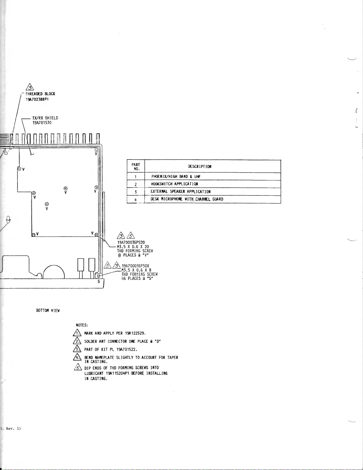
-
THREAIID 8I-OCT
1$702lttPl
SHIELD
IVRX
t9A701510
PARI
r0,
Plr€ilvHt6fl
I
KfiSilTCt{
2
ulEnnl sPE xEt APPttC
,
q
rEs( ircnoPHof,
AA
r9Azoool6P52o
Itr.5x0.5x20
THD toRntt,l6 scREt{
g
PLACES
19A700035P508
THD FORI'IIIIG
16 PLACES A
X 0.6 X 8
.5
'V'
a
SCREH
'S'
ESCTIPIIOI
BAID I Urf
AmICrTtol
ur|l!
-l
t
Tl0t
!!EL6r,lArD
\/
BOTTU
YIET
iOIES:
Hr ArD
A
sor-rl
A
ro*t oF xrT PL 1gt701522,
A
/N scm iAf,puTE sLIcHTLv T0 AccouiT FoR TApER
It c srn6.
-
ott
A
LUBntC
APPLY P€r rqr22529.
AiT
co*r€cTon
THD FoRitttc
0F
EtDs
ltT 1:nl15204P1
0,t
scREt{s
BEFoRE
prAct
s 'D'
lttTo
IIST UIi6
n ctsTInG.
 Loading...