

Page 1
g
GEPowerManagement
DGP
Digital Generator Protection Relay™
Instruction Manual
DGP Revisions:V210.12000P
V210.10000F
V211.32000J
V210.22000D
Manual P/N: GEK-100666D
Copyright © 2000 GE Power Management
All relays must be powered up at least once per year
to avoid deterioration of electrolytic capacitors and
NOTE
GE Power Management
215 Anderson Avenue, Markham, Ontario
Canada L6E 1B3
Tel: (905) 294-6222 Fax: (905) 294-8512
Internet: http://www.GEindustrial.com/pm
subsequent relay failure.
Manufactured under an
ISO9002 Registered system.
Page 2

These instructions do not purport to co ve r all de tails o r variat ions in e quipment
g
g
g
nor provide for every possible contin
ency to be met in connection with
installation, operation, or maintenance. Should further information be desired
or should particular problems arise which are not covered sufficiently for the
purchaser’s purpose, the matter should be refe rred to the General Electric
Company.
To the extent required the products described herein meet applicable ANSI,
IEEE, and NEMA standards; but no such assurance is
local codes and ordinances because they vary
reatly.
iven with respect to
Page 3

1 PRODUCT DESCRIPTION 1.1 GETTING STARTED
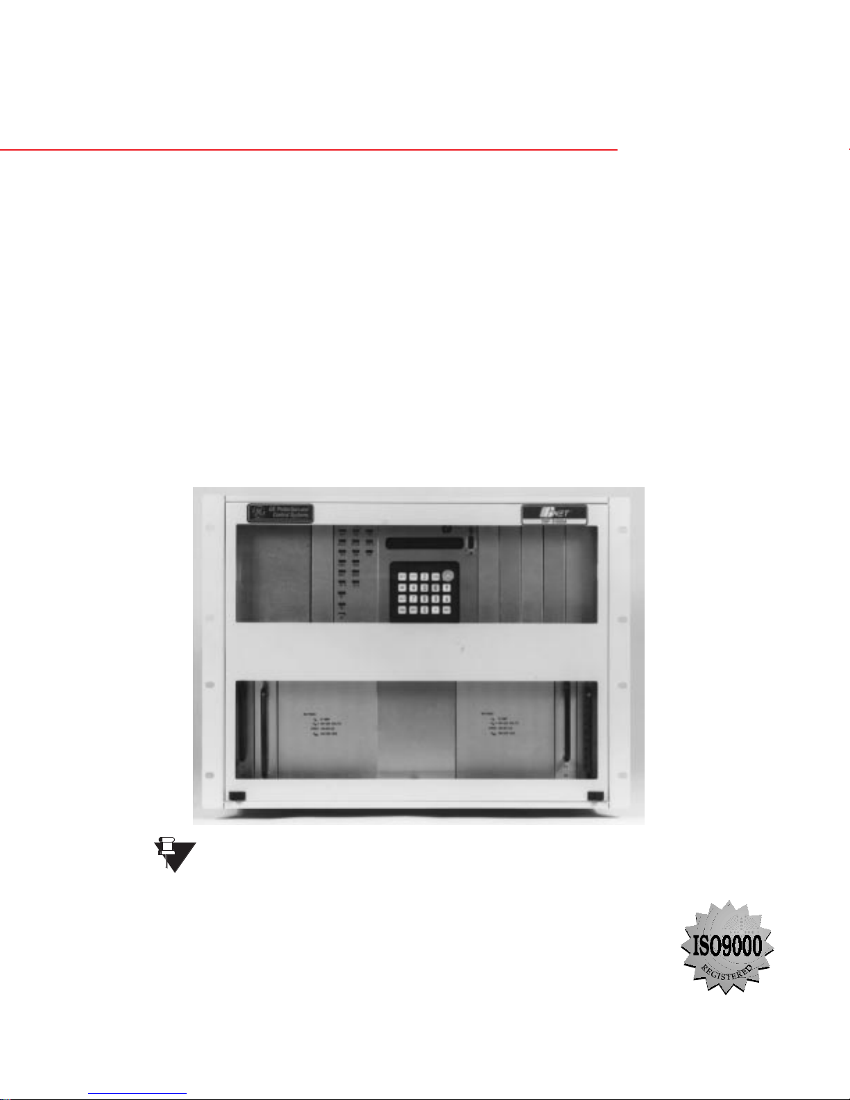
1 PRODUCT DESCRIPTION 1.1 GETTING STARTED 1.1.1 UNPACKING THE RELAY
The following procedure describes how to unpack and setup the DGP.
1. Unpack and examine the DG P Digital Gene rator Prote ction relay. Ensure each module is pro perly seated
in the relay prior to applying power.
2. Apply rated DC power to the relay at the power supply input terminals. Refer to the appropriate elementary
diagram in Section 1 .5: ELE MENTARY DIAGRAMS on page 1–23 for th e loca tion of these t ermin als. Th e
rated DC value (Vps) fo r the relay is found on the na meplate located inside the fr ont cover on the right
side.
3. The DGP settings and control functions are protected by passwords on both MMI and remote access. The
relay is shipped with the factory default passwords that mus t be changed before any setting change or
control command can be executed (GE Modem Version only). The default passwords are listed below:
MODE PAS SWORD
MMI - SETTING 1234.
MMI - MASTER 5678.
REMOTE LINK - VIEW VIEW!
REMOTE LINK - SETTING SETT!
REMOTE LINK - CONTROL CTRL!
Note that the characters "." and "!" are part of the default passwords.
1
4. Instructions on how to use the keypad to change setti ng s a nd p ut the relay into test mo de can be found in
Section 4.3.2: SETTING CHANGES on page 4–3. Complete instructions on how to operate the keypad are
found in Section 8.3: KEYPAD on page 8–3.
5. To communicate with the relay from a PC, connect the relay to a serial port of an IBM compatible computer
with a DGP null-mode m cable. Connectio n can be made either to the 25 pin D- connector on the b ack of
the relay (PL-1) or the 9 pin D-connector on the front (COM).
6. Refer to Figure 9–1: DGP COMMUNICATIONS WIRING on page 9–3 for the internal wiring of the cable.
7. GE-Link, the communications software required to access the relay from a PC, is included on the GE
Power Management Pr oduct s CD or avail able f rom the G E P ower Man agement web s ite at www.ge.com/
indsys/pm. Follow instructions in 10.1.3: INSTALLATION on page 10–1 to load GE-Link onto the PC.
8. To log into the relay, follow the instructions in Section 4.4: USING GE-LINK on page 4–5.
9. This instruction book describes functions available in DGP models with standard function groups A, B, and
C. Refer to the Nomenclature Sel ection Guide sh own below to determine func tions included in a specific
model.
GE Power Management DGP Digital Generator Protection System 1-
1
Page 4
1.1 GETTING STARTED 1 PRODUCT DESCRIPTION
g
g
1
Table 1–1: ORDER CODES
Base Unit
Current Rating
Power Supply
Test Blocks
Protocol
Functions and
Features
Revision
DGP
DGP
* * *
||||||
1
5
0
1
2
3
4
Table 1–2: DGP SELECTION GUIDE
FUNCTIONS & FEATURES A B C
Stator Differential 87G
Current Unbalance 46
Loss of Exc itation 40-1, 40-2
Anti-motorin
Overcurrent Volta
Stator Ground 64G1
Stator Ground 64G2
Stator Ground 27TN
Neutral Overcurrent 51GN Overexcitation 24 (Volts/Hz)
Overvoltage 59
Undervoltage 27 Underfrequency 81-U 424
Overfrequency 81-O 422
Accidental Engergization Logic
Sequential Trip Logic
Voltage Transformer Fuse Failure VTFF
Oscillography Data Capture
RS232 Communications Ports 222
Printer Output
IRIG-B Input
DEC1000 compatible --
c
64G1 is Fundamental Frequency Overvoltage, also known as 59GN
d
64G2 uses 3rd harmonic comparator algorithm for enhanced security
e
27TN is 3rd Harmonic Undervoltage supervised by an adjustable window of forward power.
32
e Restraint 51V
c
d
e
| | | | |
| | | | |
||||
||||
||||
||||
||||
| | |
A
| | |
B
||
A
||
B
A
B
C
1.1.2 ORDER CODES & SELECTION GUIDE
Base Unit
1 Ampere Rated Current
5 Ampere Rated Current
One Power Supply, 48 V DC
One Power Supply, 110 to 125 V DC
One Power Supply, 220 to 250 V DC
Two Power Supplies, 4 8 V DC
Two Power Supplies, 110 to 125 V DC
With T est Blocks
Without Te st Blocks
GE Modem Protocol
Modbus RTU Protcol (DGP***BCA only)
Functions and Features – see DGP selection guide below.
|
|
|
DGP Revision A Firmware
A
✔✔✔
✔✔✔
✔✔✔
212
✔✔✔
✔✔✔
✔
-
✔✔✔
✔✔✔
✔✔✔
✔✔✔
✔✔✔
✔✔✔
✔
✔✔✔
-
✔
✔✔
✔✔
✔✔
-
✔
✔
1-
2
DGP Digital Generator Protection System GE Power Management
Page 5

1 PRODUCT DESCRIPTION 1.1 GETTING STARTED
1.1.3 SPECIAL MODELS
In addition to the stan dard D GP model descri bed by the order codes a bove, s everal specia l mo dels ar e available. Some of these are shown below with a brief description.
DGP***AAA-0101 and DGP***AAA-0102
This model is similar to the standard DGP***AAA except for the following major changes:
• All digital inputs are rated for nominal voltage of 110 to 125 V DC instead of the standard 48 to 250 V DC
• The logic for function 51V is modified to remove fault detector supervision
• Seperate terminals are provided for the optional second power supply input
Refer to instruction book GEK-105552 for additional detail.
DGP***ABA-0005
This model is similar to the standard DGP***ABA except for the following major changes:
• Includes the Stator Ground 27TN function
• Includes oscillography data capture and IRIG-B input capabilities
• Suitable for application with 208 V AC nominal input
Refer to instruction book GEK-105587 for additional detail.
1.1.4 DEC 1000 CONTACT EXPANSION UNIT
1
The DEC 1000 is a relay expan sion unit for the DGP consisti ng of five form C relays and six form A relays.
These contacts can be used for signalling or alarm purposes. Any protection function available in the companion DGP relay can be sele cted for DEC output relay assignment. T he DEC 1000 is connected via the DGP
printer port PL2.
The DEC 1000 expansion unit is only compatible with the DGP
NOTE
kkkkk
C units.
GE Power Management DGP Digital Generator Protection System 1-
3
Page 6

1.2 INTRODUCTION 1 PRODUCT DESCRIPTION
1.2 INTRODUCTION 1.2.1 GENERAL
1
The DGP Digital Generator Protection™ System is a microprocessor-based digital relay system that uses
waveform sampling of curren t and voltage inputs to provide protecti on, control and monitoring of gener ators.
These samples are used to compute current and vol tage phasors that are used for the protection-function
algorithms. The DGP™ system uses a man-machine interface (MMI) and GE-Link software for local and
remote communication respectively.
This instruction book describes all the functions available in the various standard DGP models. Refer
to the SELECTION GUIDE in the previous section to determine functions included in a specific model.
1.2.2 APPLICATION
The DGP system is designed to be used on hydroelectric, gas, and steam generating units. Any size of generator can be protected with this digital system.
More detailed appl ication cons ider ations are contai ned b elow i n the rem aining head ings of this sec tion and i n
Chapter 2: CALCULATION OF SETTINGS.
A typical wiring diagram for the DGP relay is shown on the following page.
1-
4
DGP Digital Generator Protection System GE Power Management
Page 7
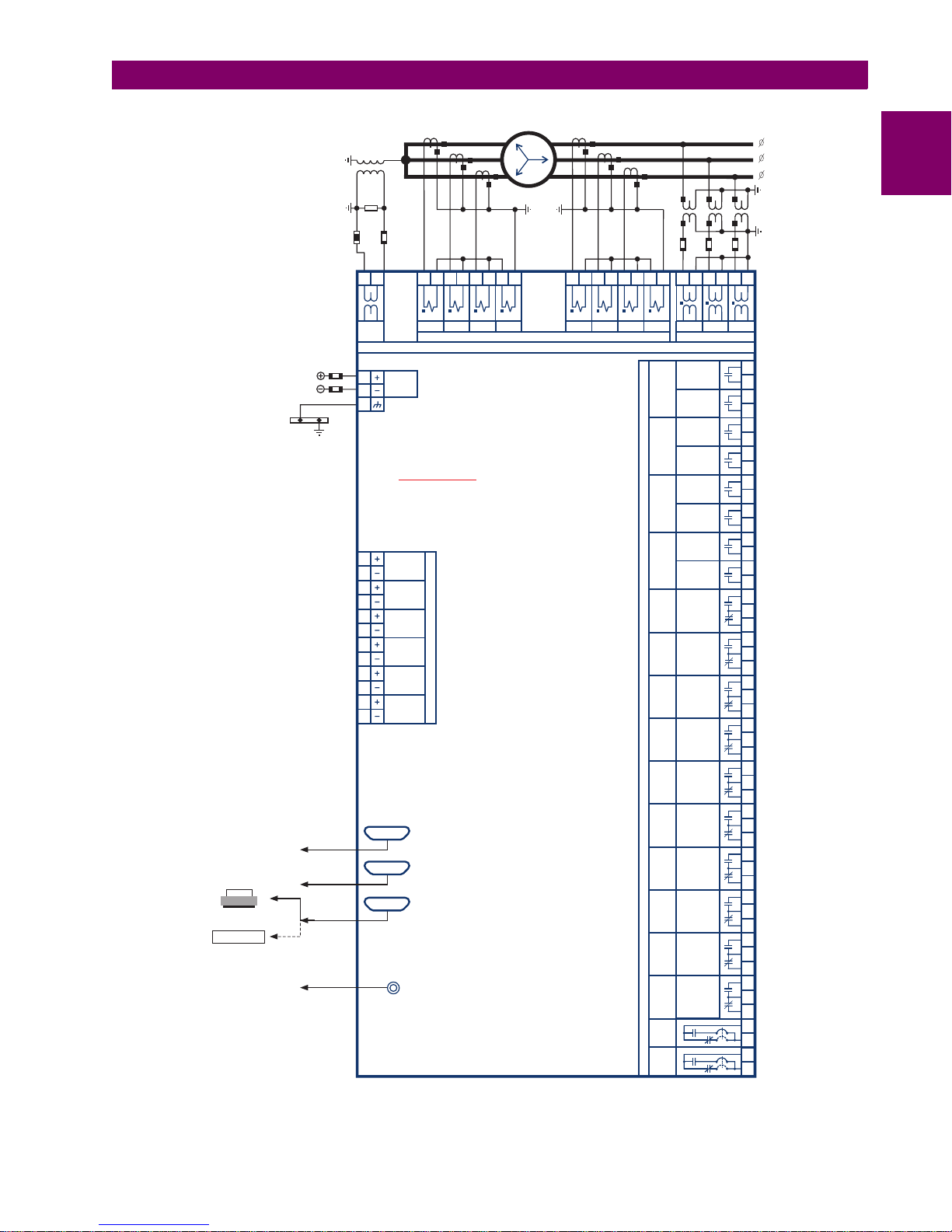
1 PRODUCT DESCRIPTION 1.2 INTRODUCTION
PRINTER
or
DEC1000
Contact Expansion
Unit
GROUND
BUS
RS-232
RS-232
PRINTER
IRIG-B
CONTROL
POWER
g
AH
AH
AH
AH
1
2
3
4
IBR IBS
IAR
GE Power Management
AG1
AG2
AH
12
VOLT
BH
14
GND
AH
11
DGP
Digital Generator Protection
BG
8
GENERATOR
BG
OFF LINE
7
BG
TURBINE
6
INLET VALVE
BG
LIMIT SWITCH
5
BG
EXTERNAL
4
TRIP 1
BG
3
BG
2
BG
1
BE
4
BE
3
BE
2
BE
1
OSCILLOGRAPH
Disable Prot.
DB9
DB25
DB25
EXTERNAL
TRIP 2
TRIGGER
EXT. VTFF/
(REAR)
(FRONT)
(REAR)
(REAR)
PL3
TS
PU
IN
PL1
PL2
A
C(B)
B(C)
BH
BH
BH
AH
AH
AH
AH
5
6
7
8
ICR ICS
INR INS
CURRENT
INPUTS
BH
1
2
3
4
IAS
A
B
C
BH
BH
BH
BH
BH
BH
BH
8
5
6
7
94G
94G1
94G2
94G3
74A
74B
74C
S
T
U
P
T
U
O
74D
74FF
DOR 12
DOR 13
DOR 9
74 NC
74 CR
POWER
SUPPLY
ALARM 1
POWER
SUPPLY
ALARM 2
9
10
VA
VOLTAGE
TRIP A
(DRY)
TRIP A
TRIP B
(DRY)
TRIP B
TRIP C
(DRY)
TRIP C
TRIP D
(DRY)
TRIP D
ALARM A
ALARM B
ALARM C
ALARM D
VT FUSE FAIL
TEST PICKUP
TEST TRIP
SPARE
SELF TEST
NON
CRITICAL
SELF-TEST
CRITICAL
BH
AH
11
12
9
VB
704753A7.CDR
AH
10
VC
BE
10
BF
10
BE
(+)
14
BF
(-)
14
BE
9
BF
9
BE
(+)
13
BF
(-)
13
BE
8
BF
8
BE
(+)
12
BF
(-)
12
BE
7
BF
7
BE
(+)
11
BF
(-)
11
AG
14
AF
14
AE
14
AG
13
AF
13
AE
13
AG
12
AF
12
AE
12
AG
11
AF
11
AE
11
AG
10
AF
10
AE
10
AG
6
AF
6
AE
6
AG
5
AF
5
AE
5
AG
9
AF
9
AE
9
AG
8
AF
8
AE
8
AG
7
AF
7
AE
7
BF
5
BE
5
BF
BF
6
6
BE
BF
6
6
1
GE Power Management DGP Digital Generator Protection System 1-
Figure 1–1: TYPICAL WIRING DIAGRAM
5
Page 8
1.3 PROTECTION FEATURES 1 PRODUCT DESCRIPTION
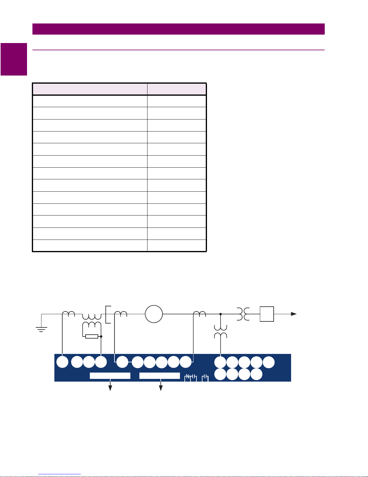
1.3 PROTECTION FEATURES 1.3.1 DESCRIPTION
1
The following protection functions are included with the DGP system.
Table 1–3: DGP PROTECTION FUNCTIONS
PROTECTION FUNCTION ANSI CODE(S)
Stator Differential 87G
Current Unbalance 46
Loss of Excitation 40
Anti-Motoring 32
Time Overcurrent with Voltage Restraint 51V
Stator Ground 64G1, 64G2, 27TN
Ground Overcurrent 51GN
Over-excitation 24
Overvoltage 59
Undervoltage 27
Over and Underfrequency 81
Voltage Transformer Fuse Failure VTFF
Accidental Energization AE
A single-line diagram for the DGP is shown below.
GEN.
51GN
27NT
64G2
64G1
RS232
87G
VTFF
51V
32
RS232
40
46
24
VTFF
64G2
51V
GSU
Transf.
32
40
27
59
52G
81
TO
POWER
SYSTEM
DGP
To
MODEM
1-
6
DGP Digital Generator Protection System GE Power Management
To
ALARM
LAPTOP
PC
TRIP
Figure 1–2: SINGLE LINE DIAGRAM
Page 9

1 PRODUCT DESCRIPTION 1.3 PROTECTION FEATURES
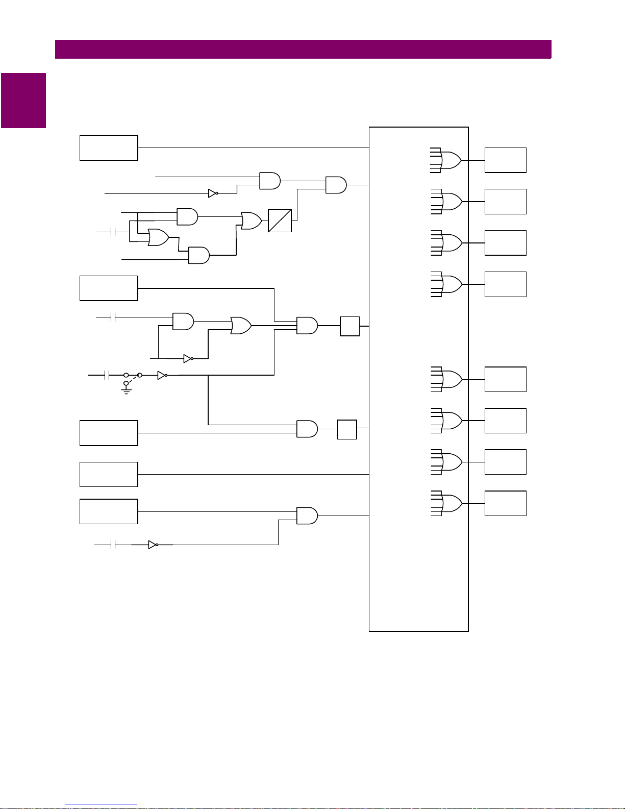
1.3.2 STATOR DIFFERENTIAL (87G)
This function provides high -speed pr otection of the genera tor stat or during inter nal pha se-to- phase an d threephase faults. It uses a product-restraint algorithm with dual-slope characteristic described in Section 2.3.2:
STATOR DIFFER ENTIAL 87G on page 2–13. R efer to Figure 1–3: S IMPLE LOGIC DIAG RAM – 87G, 32 , 27 ,
59, AND AE on page 1–12 for the logic diagram of this function.
Function 87G will not operate for turn-to-turn faults in the machine windings.
It will also not operate for single-phase-to-ground faults if the system is ungrounded or high-impedance
grounded. Phase-to-ground protection by this function requires that the neutral of the machine (or another
machine operating i n parallel) be grounded. A small portio n of the windi ng next to th e neutral will no t be protected, the amount being determined by the voltage necessary to cause minimum pickup current to flow
through the neutral-to-g round impedance. Current-limiting devices in the neutral-ground c ircuit increase this
impedance and will decrease the ground-fault-protection coverage of this function.
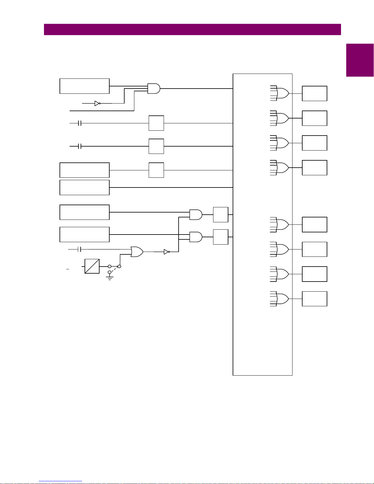
1.3.3 CURRENT UNBALANCE (46T)
There are several cause s of generator unba lance . Som e of th ese i nclude unbala nced loads , unbal ance d sy s-
I
tem faults, and/or op en circuits. Th e negative-seque nce component (
) of stator current is directly r elated to
2
this unbalance and sets up a co unter-rota tin g flux fie ld in the mach ine . This in turn ca uses local he ating in the
rotor iron. The c apability of machines to withstand heating caused by unbalance current s is typically experessed in terms of an constant, and is supplied by the manufacturer of the machine.
The current unbalance tri p function (46T) of the DGP provides operating-tim e characteristics expressed as
2
I
T
= K, as shown in Fig ure 2 –6: TIME CURRENT CHARACTE RIS TIC O F 4 6T FUNC TI ON on pa ge 2–1 9. A
2
2
I
T
2
linear reset characteristic is incorporated to approximate the machine cooling following an intermittent currentunbalance condition. In addition to 46T, the DGP s ystem also includes a current-unba lance alarm function,
46A, which is operated by the nega tive-sequence component (I2) with an adj ustable pickup and time delay.
See Figure 1–4: SIMPLE LOGIC DIAGRAM – 46, 40, AND 51V on page 1–13 for the logic diagram.
1
1.3.4 LOSS OF EXCITATION (40)
This function is used to detect loss of excitation on synchronous machines. It includes two mho characteristics
looking into the machine, each with adjustable reach, offset, and time delay. Logic is provided to block this
function by presence of a negative-sequence voltage (indic ating a voltage trans former fuse failure VTFF condi tion) and/or an external VTFF Digital Input DI6 (see Figure 1–4: SIMPLE LOGIC DIAGRAM – 46, 40, AND 51V
on page 1–13).
Excitation can be los t due to ina dverten t trippi ng of the fi eld brea ker, open or short circui t on the fie ld wind ing,
regulator failure, or loss of the sour ce to the fie ld win ding. Loss of exci tation can b e dama ging to the m achin e
and/or detrimental to t he operation o f the sys tem. When a sy nchronous generator l oses exci tation, it will tend
to act as an induction generator: it will run above normal speed, operate at reduced power and receive its excitation (VARS) from the system. The impedance seen by a relay looking in to a generator will depend on the
machine characteristics, the load flow prior to the loss of excitation, and the type of excitation failure.
Studies indicates that first zone mho function (40-1) can be set to detect severe cases of excitation failure with
a shorter time d elay, whereas the second zone (40-2) c an be set to det ect all the excitation failure cases. A
longer time delay s etting is required for t he 4 0- 2 fu nc tio n fo r se cu ri ty duri ng sta ble power system swin g c ond itions. Figure 2–7: MHO CHARACTERISTICS FOR 40-1 & 40-2 FUNCTIONS on page 2–21 shows the characteristics of this function.
GE Power Management DGP Digital Generator Protection System 1-
7
Page 10

1.3 PROTECTION FEATURES 1 PRODUCT DESCRIPTION
1.3.5 ANTI-MOTORING (32)
1
On a total or partial loss of prime mover, if the power generated is less than no-load losses of the machine, real
power will start flowing into the generator. Typical motoring power of different kinds of prime movers are shown
in the table below. For a specific application, the minimum motoring power of the generator should be obtained
from the supplier of the unit.
The DGP system includes a reverse power function with adjustable time-delay. Either one or two (32-1 & 32-2)
independent setpoints are incorporated depending on the model number.
Table 1–4: TYPICAL MOTORING POWER
TYPE OF PRIME
MOVERS
Gas Turbine 10 to 100
Diesel 15 to 25
Hydraulic Turbine 2 to 100
Steam Turbine 0.5 to 4
The 32-1 can be configured as a part of sequential tripping logic as shown in Figure 1–3: SIMPLE LOGIC DIAGRAM – 87G, 32, 27, 59, AND AE on page 1–12. If the sequential trip logic is used, 32-1 is enabled when closing of turbine inlet v alves is indicated by digital in put DI2 following a turbine trip . The trip sequence is then
continued when timer TL1 times out. The 32-2, if included, is not dependent on the DI2 and is primarily
intended to provide bac k up t o th e s equ ent ial trip . If the sequential trip is no t en abl ed, the 32-1 can be used as
anti-motoring similar to 32-2.
A system must be protected against prolonged generator contribution to a fault. The DGP incorporates a timeovercurrent functio n with vo ltage re straint (51V ) to provi de part of the syst em backu p protecti on. As s hown in
Figure 1–4: SIMPLE LOGIC DIAGRAM – 46, 40, AND 51V on page 1–13, this function is supervised by a fault
detector and VTFF. The VTFF supervision can be by an internal an d/or external (DI6) VTFF fun ction. See Section 2.3.7: OVERCURRENT WITH VOLTAGE RESTRAINT (51V) on page 2–22 for the characteristic curves of
the 51V . Note that a separate algorithm is processed for each phase, with the restraint provided by corresponding phase voltage. The restraint is proportional to the magnitude of the voltage and is independent of the phase
angle. A linear reset characteristic is incorporated for this function.
MOTORING POWER IN %
OF UNIT RATING
1.3.6 TIME OVERCURRENT WITH VOLTAGE RESTRAINT 51V
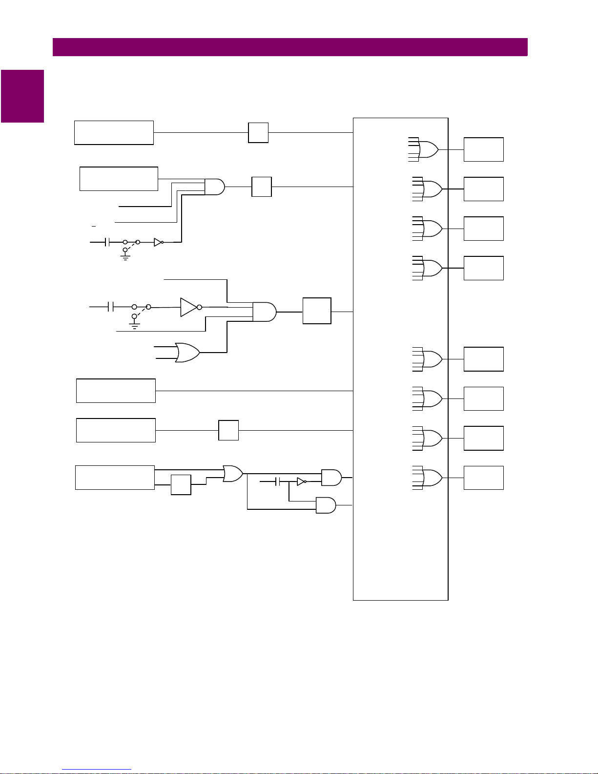
This function consists of two overlapping zones (64G1 and 64G2/27TN) to detect stator ground faults in a highimpedance-grounded generator system. The 64G1 is standard in all DGP models; however, the 64G2/27TN
function is provided in some models only. Together, the two zones cover 100% of the stator windings. See Figure 1–5: SIMPLE LOGIC DIAGRAM – 64G1, 64G2, 51GN, AND 24 on page 1–14.
Normally the generator-stato r neutral has a potential cl ose to ground. With the occurren ce of a stator ground
fault, a potential increase will occur on the neutral for all faults except those near the neutral. 64G1 uses a fundamental-frequency neutral overvoltage to cover about 95% of th e stator winding, depending on the pic kup
voltage setting. Alternately, 64G1 can be used as a generator-bus ground detector in a high-impedance
grounded or an ungrounded system. For this application, the VN input must be a zero-sequence voltage
derived from the generator bus, and functions 64G2/27TN must be disabled.
1-
8
DGP Digital Generator Protection System GE Power Management
1.3.7 ST ATOR GROUND (64G/27TN)
Page 11

1 PRODUCT DESCRIPTION 1.3 PROTECTION FEATURES
64G2 is based on the perc entage of third-harmonic vo ltage at the generator neutral (VN 3) compared to the
total third-harmonic vol tage gener ated. This func tion is design ed to cover 15 % of the neutral end o f the stator
windings, and is supervised by fundamental and third-harmonic voltage thresholds. These thresholds are fixed
at 30 and 0.5 volts respectively. The third-harmonic comparator method eliminates the need to know the generator harmonic characteristic to use or set this function.
proper operation of 64G2
27TN is the third- harmonic neutral u ndervoltage functio n with a forward power supervision and can be used
with either wye or delta connected VTs. The percentage of stator windings covered by this function depends on
its threshold setting as well as the VN3 generated b y the machine at the time of th e fault. The magnitude of
VN3 under normal condi tions is a function of several factors, su ch as type of generator, load current, load
power factor, system status, etc. It can be very small (nearly zero) under some conditions. T o enhance security
during low VN3 vo lta ge conditions, this f unc tio n can b e i nhi bi ted by a se tt able window of forward power. However, it should be noted that other condi tions influenci ng the VN3 vol tage may make 2 7TN insecu re. In these
cases, function 64G 2 (available in some models; see the DGP nomenclature guide) or some other means
should be considered.
Digital input DI1 can be co nfigured to bloc k 64G2/27T N when the gener ator is off-line. Thi s provision is made
to enhance security of the functions under conditions such as static start of a gas turbine generator. Temporary
ungrounding of generator neutral during the static start can look like a ground fault near the neutral.
.
Note that wye-connected VTs are required for
1.3.8 GROUND OVERCURRENT (51GN)
1
51GN is an inverse overcurrent function available in some models. It can be used to detect stator ground faults
in a high or low resist ance grounded generator sy stem. See Fig ure 1–5: SIM PLE LOGIC DIA GRAM – 64G1,
64G2, 51GN, AND 24 on pa ge 1–14 for simplified logic diagram and Figure 2 –16: 51GN TIME-CURRENT
CHARACTERISTICS on page 2–39 for the inverse time-current characteristics.
This function uses current INR which can be derived by residual connection or by using a generator neutral CT
as noted in F igures 1–9: ELEMENTARY DIAGRAM WITH TE ST BLOCKS, WYE VTs and 1–12: ELEMENTARY DIAGRAM WITHOUT TEST BLOCKS, DELTA VTs.
Since this function is independen t of the phase current inputs , it can alterna tely be connect ed to a CT in the
neutral of the generator step-up transformer.
1.3.9 OVEREXCITATION (24)
Overexcitation can b e caus ed by reg ulator failure , load r eject ion, or an exce ssiv e excit ation wh en the ge nerator is off-line. It can also resul t from decr easing spee d while the regulator o r an operator a ttempts to m aintain
rated stator voltage. The Volts/Hertz quantity is proportional to magnetic flux in the generator and step-up
transformer cores, and is use d to detect the overexcitation condition. Se e Figure 1–5: SIMPLE LOGIC DIAGRAM – 64G1, 64G2, 51GN, AND 24 for details.
The overexcitation protection includes trip (24T) and alarm (24A) functions. 24T consists of an inverse function
and an instantaneous fu nction with time-delay characteris tics. The combination of these two char acteristics
allows the 24T setting to cl osely follow the generator and/or ste p-up transformer V/Hz limit curve. Bo th 24A
and 24T are computed for each of the three phase voltages (see Table 2–3: 24A VOLTAGES on page 2–30).
Function 24T can be c onfigu red to operate d ifferent ou tput re lays for gene rator on -lin e and o ff-line condi tions.
This function incorpora tes a user-settable li near reset character istic to mimic machi ne cooling. The figu res in
Section 2.3.12: OVEREXCITATION TRIP (VOLTS/HERTZ: 24T) show the characteristics of this function.
GE Power Management DGP Digital Generator Protection System 1-
9
Page 12

1.3 PROTECTION FEATURES 1 PRODUCT DESCRIPTION
1.3.10 OVERVOLTAGE (59)
1
This function consists of a positive-sequence overvoltage with an user selectable inverse or definite time characteristic. See Figure 1–3: S IMPLE LOGIC DIAGRAM – 87G, 32, 27, 59, AND AE on page 1–12 fo r the logic
diagram and Figure 2–15: 59 TIME-VOLTAGE CHARACTERISTICS on page 2–35 for the inverse time-voltage
characteristics. A l inear reset charact eristic is incorp orated for this function. The overvoltage functi on can be
considered as a backup to the Volts/Hz function. Some possible causes of this cond ition are a system dis turbance or regulator failure.
1.3.11 UNDERVOLTAGE (27)
This function consists of a positive-sequence undervoltage with an user selectable inverse or definite time
characteristic. See Figur e 1–3: SIMPLE LOGIC DIAG RAM – 87G, 32, 27, 59, AND AE on p age 1–12 for the
logic diagram and Figu re 2–17: 27 TIME -VOLTAGE CHARACTER ISTICS on pa ge 2–40 for the inv erse timevoltage characteristics. A linear reset characteristic is incorporated for this function.
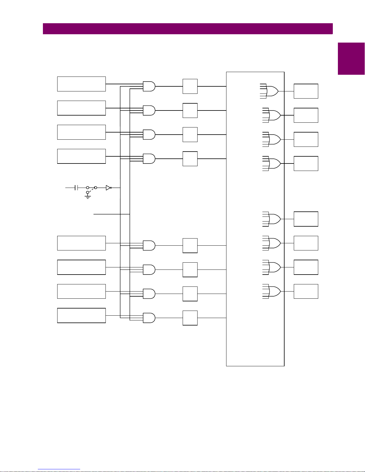
1.3.12 OVER AND UNDERFREQUENCY (81)
This function provides over and underfrequency protection, each with an adj ustable time delay. Two or four
over and underfrequency ste ps are provided dep ending on the model. Al l frequency functi ons are supervise d
by an adjustable positive-sequence voltage level. This undervoltage cut-off level and/or digital input DI1 can be
used to block the freq uency functions during sta rt-up. Fr equency dis turbance c an occur due to a system fault
or islanding of the unit or an unconnected unit can operate at abnormal frequency due to malfunction of speed
control. Figure 1 –6: SIMPLE LOGIC DIA GRAM – 81-O A ND 81-U on page 1 –15 show s the l ogic diag ram for
this function.
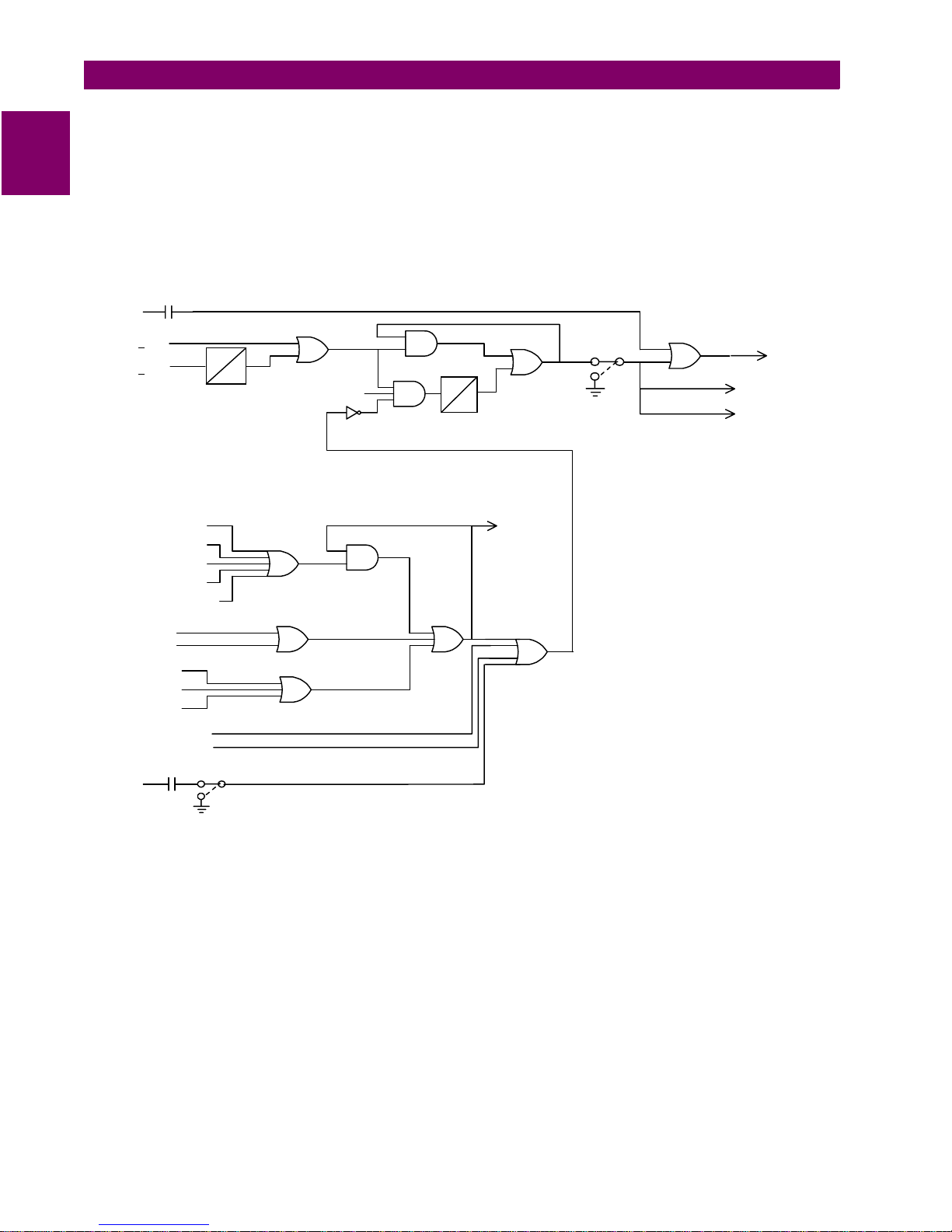
1.3.13 VOLTAGE TRANSFORMER FUSE FAILURE (VTFF)
Functions 40 and 51V may operate for a full or partial loss of AC potential caused by one or more blown fuses.
The DGP makes provisions to block tripping by these functions when a fuse failure is detected; all other protection functions are a llowe d to t rip. Fig ure 1–7: SIMP LE L OGIC DIA GRAM – VT F USE FAILURE on pag e 1–1 6
shows the logic diagram for the VTFF function.
If AC potential is lost on one or more phas es, the negative-seque nce voltage (V2) rise s and/or the positivesequence voltage ( V1) drops. Either V2 > 15V or V1 < 50V pro vides a bas ic indic ation of th e VTFF con dition.
This signal is supervi sed by a Distur bance Dete ctor (DD) and gene rator posit ive-se quence cu rrent (I1) dete ctor (see three-inp ut AND gate on the log ic diagram). Supervision by the DD and I1 signa ls provide security
against false ope ration du ring fault a nd genera tor out of service conditio ns respec tively. Security is enhance d
by use of the A/0 and B/0 timers shown in the logic diagram.
Signal DD is derived from a combination of sequence current levels, change in levels, and pickup flags of various protection functions as shown in the logic diagram.
The VTFF logic allows integration of an external VTFF contact. Either of the two fuse-failure signals or both
signals can be configured to block tripping of functions 40 and 51V.
Detection of VTFF energizes the 74FF (Fuse Failure alarm) relay, de-energizes the 74CR (critical alarm) relay,
and turns the status LED red, even though all protection functions except 40 and 51V are unaffected.
1-
10
DGP Digital Generator Protection System GE Power Management
Page 13

1 PRODUCT DESCRIPTION 1.3 PROTECTION FEATURES
1.3.14 ACCIDENTAL ENERGIZATION (AE)
The DGP includes logic to detect accidental energization of the gener ator (see Figure 1–3: SIMPLE LOGIC
DIAGRAM – 87G, 3 2, 27, 59, AND AE on page 1–12). When a generator is energized while at standstill or
reduced speed, it behaves and acc elerates as an induction mot or. The machine terminal voltage and current
during such an event will be a function of generator, transformer, and system impedances.
An instantaneous over cu rren t si gna l (50) is used to det ect t he acci de ntal ener g izati on. T his s ig nal is arm ed by
a logic signal de rived from positive- sequence voltage and GEN O FF LINE input DI1. These two "arming " signals can be confi gured in AND or O R mode by Se tting 2703:
after the generator is taken out of service. The logic automatically disarms itself during a normal start-up
sequence when the voltage detector picks up and/or the generator is on-line.
For the AE logic to perform, special precautions must be taken to ensure that the DGP system and associated
trip circuits remain in service when the generator is out of service. Additionally, the generator off-line input, DI1,
must be reliable. It should also be noted that the pickup flag of function 51V is used as signal 50; therefore this
logic will automatically be disabled if function 51V is disabled.
AE ARM
. The 50 function is armed 5 seconds
1
GE Power Management DGP Digital Generator Protection System 1-
11
Page 14
1
1.3 PROTECTION FEATURES 1 PRODUCT DESCRIPTION
Stator
Differential
50 (51V Pickup Flag)
VTFF
V1 < 30V
DI1
(+)
Gen. Off-line
OR
AE ARM
Reverse Pwr.
No. 1
(+)
DI2
Turbine Inlet Valve
Closed
Seq. Trip Enabled
DI1
(+)
Gen.
Off-Line
SELBKDI1
Reverse Pwr.
No. 2 (1)
AND
AND
AND
AND
PU
OR
PU=5 sec
DO=0.25 sec
DO
ANDOR
AND
AND
AND
TL1
TL2
87G
87G
AE
AE
32-1
32-2
OR
OR
OR
OR
OR
OR
TRIP A
94G
TRIP B
94G1
TRIP C
94G2
TRIP D
94G3
ALARM
74A
ALARM
74B
Overvoltage
59
Undervoltage
(+)
(1)
DI1
Gen.
Off-Line
AND
27
NOTES:
(1) Indicates an optional function (includes associated logic). Refer to
CONFIGURABLE
DGP nomenclature selection guide for available functions in a
specific model.
(2) Each of the available protection functions can be configured to
operate any combination of the 8 output relays (4-Trip and 4-Alarm).
Figure 1–3: SIMPLE LOGIC DIAGRAM – 87G, 32, 27, 59, AND AE
LOGIC (2)
OR
OR
ALARM
74C
ALARM
74D
1-
12
DGP Digital Generator Protection System GE Power Management
Page 15
1 PRODUCT DESCRIPTION 1.3 PROTECTION FEATURES
1
Overcurrent
(voltage restraint)
VTFF + DI6
FD
(+)
(+)
DI3
External Trip - 1
DI4
External Trip - 2
Current Unbalance
(Alarm)
Current Unbalance
(Trip)
Loss of Excitation
Zone 1
Loss of Excitation
Zone 2
DI6
(+)
V
2
Ext. VTFF
>
PU
15V
PU=3 Samples
DO=5 Samples
DO
ENA
SELV2SUP
DIS
OR
AND
TL21
(1)
TL22
(1)
TL14
87G
51V
OR
TRIP A
94G
AE
TRIP B
94G1
TRIP C
94G2
TRIP D
94G3
DI3
DI4
46A
OR
OR
OR
46T
TL12AND
TL13AND
40-1
40-2
OR
OR
OR
ALARM
74A
ALARM
74B
ALARM
74C
OR
ALARM
74D
NOTE:
(1) Timers TL21 and TL22 are available in models DGP***ACA only.
(2) Each of the available protection functions can be configured to
operate any combination of the 8 output relays (4-Trip and 4-Alarm).
CONFIGURABLE
LOGIC (2)
DSPLGC2.VSD
Figure 1–4: SIMPLE LOGIC DIAGRAM – 46, 40, AND 51V
GE Power Management DGP Digital Generator Protection System 1-
13
Page 16
1
1.3 PROTECTION FEATURES 1 PRODUCT DESCRIPTION
Stator Ground
Zone 1
Stator Ground
Zone 2 (1)
VP3 > 0.5V
V1
30V
>
DI1
(+)
Gen.
Off-Line
V
≤
N3
GEN. OFF-LINE
(+)
DI1
V
25V
≥
1
SELBKDI1
27TN PICKUP
SELBKDI1
POWER < FORPWR-L
POWER > FORPWR-H
Neutral Overcurrent
(1)
OR
AND
TL4
TL5
AND
TL20
64G1
64G2
27TN
(1)
51GN
OR
OR
OR
OR
OR
OR
TRIP A
94G
TRIP B
94G1
TRIP C
94G2
TRIP D
94G3
ALARM
74A
ALARM
74B
Overexcitation
(Alarm)
Overexcitation
(Trip)
Time
Inst
TL7
TL6
OR
(+)
DI1
Gen.
Off-Line
AND
AND
24A
24T
(On-Line)
24T
(Off-Line)
NOTES:
(1) Indicates an optinal function (includes associated logic). Refer to
DGP nomenclature selection guide for available functions in a
specific model.
CONFIGURABLE
(2) Each of the available protection functions can be configured to
operate any combination of the 8 output relays (4-Trip and 4-Alarm).
Figure 1–5: SIMPLE LOGIC DIAGRAM – 64G1, 64G2, 51GN, AND 24
LOGIC (2)
OR
OR
ALARM
74C
ALARM
74D
1-
14
DGP Digital Generator Protection System GE Power Management
Page 17
1 PRODUCT DESCRIPTION 1.3 PROTECTION FEATURES
1
Under Frequency
Set Point - 1
Under Frequency
Set Point - 2
Under Frequency
Set Point - 3 (1)
Under Frequency
Set Point - 4 (1)
DI1
(+)
Gen.
Off-Line
SELBKDI1
V1 > UVCUTOFF
Over Frequency
Set Point - 1
AND
AND
AND
AND
AND
TL8
TL9
TL10
TL11
TL15
81-1U
AE
81-2U
81-3U
81-4U
81-1O
OR
OR
OR
OR
OR
OR
TRIP A
94G
TRIP B
94G1
TRIP C
94G2
TRIP D
94G3
ALARM
74A
ALARM
74B
Over Frequency
Set Point - 2
AND
TL16
81-2O
Over Frequency
Set Point - 3 (1)
AND
TL17
81-3O
Over Frequency
Set Point - 4 (1)
AND
TL18
81-4O
NOTES:
(1) Indicates an optional function (includes associated logic). Refer to
DGP nomenclature selection guide for available functions in a
specific model.
(2) Each of the available protection functions can be configured to
operate any combination of the 8 output relays (4-Trip and 4-Alarm).
CONFIGURABLE
Figure 1–6: SIMPLE LOGIC DIAGRAM – 81-O AND 81-U
OR
OR
LOGIC (2)
ALARM
74C
ALARM
74D
GE Power Management DGP Digital Generator Protection System 1-
15
Page 18
1
1.3 PROTECTION FEATURES 1 PRODUCT DESCRIPTION
DI6
(+)
External VTFF
V2
15V
>
50V
V1
<
51V Pickup Flag
40 Pickup Flag
87G Pickup Flag
51GN Pickup Flag
21 Pickup Flag (Fut.)
I0 ≥ 0.6 / *
∆
∆
I2 ≥ 0.6 / *
∆
I0| ≥ 0.2 / *
|
I1| ≥ 0.2 / *
|
∆
|∆I2| ≥ 0.2 / *
64G1 Pickup Flag
64G2 Pickup Flag
DI1
(+)
Gen.
Off-Line
PU
PU=9000 samples
DO=0
SELBKDI1
DO
OR
I1 > 0.1/*
OR
OR OR
OR
AND
AND
AND
PU
DO
PU = 36 samples
DO = 0
FD
OR
Supervise
51V,
21(Future)
OR
DD
ENA
DIS
VTFF
VTFF + DI6
OR
Supervise
51V,
21(Future)
VTFF Alarm
Critical Alarm
NOTE:
* = 1 FOR 5 AMP RATED DGPs.
* = 5 FOR 1 AMP RATED DGPs.
Figure 1–7: SIMPLE LOGIC DIAGRAM – VT FUSE FAILURE
1-
16
DGP Digital Generator Protection System GE Power Management
DGP_VTFF.VSD
Page 19

1 PRODUCT DESCRIPTION 1.4 OTHER FEATURES
1.4 OTHER FEATURES 1.4.1 INPUTS
The DGP system takes eight current and four voltage inputs (refer to Section 1.5: ELEMENTARY DIAGRAMS).
The input currents in terminals BH1, BH3, and BH5 (I
, IBS, and ICS) are used to process functions 46, 40, 32,
AS
and 51V. As noted in the elementary diagrams, these currents can be derived from system side or neutral side
CTs as de sired. Either the sy stem or n eutral s ide CTs can be used fo r these functi ons if the Stator D ifferential
(87G) function is enabled.
The current input s I
and INR are derived from th e resid ual connec tions of t he respe ctive phas e CTs and do
NS
not require dedicated neutral CTs. Zero-sequence current at system and/or neutral side of the generator stator
windings is calculated and then compared with the measured I
and/or INR values by the DGP as a part of the
NS
background self-test.
The I
icated neutral CT can be used for the input I
The DGP phase volta ge i npu ts c an be wye or delta and are derived f ro m the gen er ato r term in al v ol tag e. V
current is used to process the 51GN function (not available on DGP***AAA models). If desired, a ded-
NR
NR
.
is
N
derived from the generator neutral grounding transformer.
A time synchronizin g signal can be connected to the DGP for syn chronization to within 1 ms of a referenc e
clock. Either IRIG-B or GE's G-NET system signal can be used. This signal is required only if it is necessary to
synchronize the DGP to an external reference clock.
Six digital inputs can be connected to the DGP. Two of these inputs (DI3 and DI4) are a ssigned for possi ble
routing of external trip/alarm signals to take advantage of the output configuration or sequence-of-events capability. Generator off-line (DI1), turbine inlet-valve-close indication (DI2), and external VTFF (DI6) inputs are
used for various relay logic functions. A contact input, (DI5), can also be used to trigger the optional oscillography feature. In some models, the DI6 input can be configured as external VTFF or DISABLE ALL PROTECTION (refer to Section 1.5: ELEMENTARY DIAGRAMS for details).
1
The digital input circuits are universally rated for nominal control voltages of 48 to 250 V DC.
1.4.2 OUTPUT RELAYS
The DGP system includes ei ght user-configur able output relays. Four of these relays (94G, 94G1, 94G2 and
94G3) are high speed (4 ms) trip-duty rated with two form A contacts each. The remaining four (74A, 74B, 74C
and 74D) are standard speed (8 ms) with one form C contact each, intended for alarms. Each of the protection
functions can be configured to operate any number of these output relays. The trip outputs are intended for, but
not limited to, the following purposes:
• 94G: trip a lockout relay to shut down the machine
• 94G1: trip field breaker
• 94G2: trip main generator breaker or breakers
• 94G3: operate a lockout relay to trip turbine.
In addition to the configu rable output relays, fi ve pre-defined alarm duty relays with one form C c ontact each
are included. These alar m relays inc lude critical and non-cri tical self- test alarms ( 74CR and 74NC) , the VTFF
alarm (74FF), and loss of power-supply alarms (PS1 and PS2). The form C contact of each of the alarm relays,
except PS1 and PS2, are wired out to the terminal block. A hard wire jumper is used to select either the form A
or the form B conta ct of each of the PS1 and P S2 relays, as shown in Figure 3–3: DGP POWER S UPPLY
MODULE on page 3–4.
All alarm relays, wi th the exc eption of 74CR, PS1 a nd PS2, are e nergized wh en the appr opriate al arm conditions exist. Relays 74CR, PS1 and PS2, however, are energized under no rmal conditions and will dro p out
when the alarm conditions exist.
GE Power Management DGP Digital Generator Protection System 1-
17
Page 20

1.4 OTHER FEATURES 1 PRODUCT DESCRIPTION
Also included are two additional relays (TEST PICKUP and TEST TRIP) that can be configured to operate by a
selected protectio n function pi ckup flag an d trip output. T hese two outpu ts are inten ded to facilitate testing of
1
the selected protection function.
A Contact Expansi on Unit is al so av ailable whic h can be u sed with DGP* **ACA models . The Gene ral El ectric
DEC1000 Contact Expa nsion Unit provides eleven a dditional output relays that can be factory config ured to
user specifications. Refer to the GE Power Mana gement Product Ca talog, the GE Pow er Management Products CD, or instruction book GEK-105561 for additional details on the DEC1000.
1.4.3 START-UP SELF-TESTS
The most comprehens ive testing of the DGP is perform ed during powe r-up. Since the DG P is not perform ing
any protection activities at that time, tests (such as RA M tests) that would norm ally be disruptive to ru n-time
processing are per formed during the start-up. Al l processors p articipate in th e start-up sel f-test process. T he
processors commun ic ate th eir results to each other so that any failures foun d c an be r epo rt ed to t he us er an d
to ensure each processor successfully completes its assigned self-tests before the DGP system begins protection activity.
During power-up, the micr oprocessors perfor m start-up self-test s on their associated ha rdware (PROM, local
RAM, shared RAM, interrup t controller, timer chip, serial and parallel I/O ports, non-volatile memory, analog
and digital I/O circuitry, MMI hardware, etc.). In addition, the DGP system verifies that the PROM version numbers in all processor boards are compatible. The components tested at start-up are listed in Table 6–1: ST ARTUP SELF-TESTS on page 6–2.
In most cases, if any critical self-test failure is detected, the DGP will not continue its start-up but will not cause
a reset. An attempt will be made to store the sy stem status, to initi alize the MMI and remote communications
hardware/software for communication status, and to print a diagnostic message. The critical alarm relay will be
de-energized.
If no failures are detected, the DGP completes initialization of its hardware and software. Next, each processor
board (DAP and S SP) will enable the outputs. As a f inal step, the DG P checks the res ults of all the te sts to
determine whether to turn the front panel status LED to green.
The start-up procedure takes approximately one minute. As soon as the SSP successfully completes its
PROM test and in itializ es the disp lay h ardwa re, th e mes sage
system initialization is completed, the display is blanked and the relay begins acquiring and processing data.
Each of the processors has "idle time" when the system is in a quies cent state; that is, when the DGP is not
performing fault or po st-fa ult proc essi ng. During this i dle tim e, each proce ssor pe rforms backg round self-tes ts
that are non-disruptive to the foreground proc essing. If any back ground self-tes t fails, the test is repeat ed. To
declare a component FAILED , the test must fail three consec utive times. In the case of criti cal failures, the
DGP forces a self reset to resume operation again after an intermittent failure. The reset activities are identical
to the start-up activities except that not all start-up self-tests are performed.
A reset is not reported to the user by the DGP system. If the reset is successful, no message is printed, no failure status is recorded, an d the critical alarm is not generated. However, during the reset proc edure, the red
LED on the MMI panel will light and a failure code ma y appear on the MM I displa y. If the reset is not successful, the processor boar d will be shut down, leaving the MMI panel displaying the error information. Ref er to
Section 6.4: ERROR CO DES on page 6–7 fo r error codes. To prevent continual resets in the ca se of a solid
failure, both hardware and software will permit only four resets in a one hour period. On the fifth reset, the DGP
will not perform initialization, but will attempt to initialize MMI, communications, and the critical alarm output, as
in the case of a start-up with a critical self-test failure.
INITIALIZING
will be displayed. When the DGP
1.4.4 RUN-TIME SELF-TESTS
1-
18
DGP Digital Generator Protection System GE Power Management
Page 21

1 PRODUCT DESCRIPTION 1.4 OTHER FEATURES
The components tested in the backg round are listed in Table 6–2: RUN-TIME BACKGROUND SELF-TESTS
on page 6–3. The testing of I/O hardware is done in the foreground so the processors know when a given component or port is in u se and therefore n ot available f or testing. The com ponents tested in the foreground are
listed in Table 6 –3: RUN-TIME FOREGROUND SELF-TESTS on p age 6–3. Some foreground tests are performed every sample period while others are performed less frequently. As with background self-tests, any
failed test is repeated and must fail three consecutive times to be considered a failure. Although not specifically
a self-test, trip circuit c onti nui ty mo nit or ing is a lso p er forme d a s a foreg ro und tes t. Refe r to th e T RIP CIR CUIT
MONITOR section below.
In addition to backgroun d self-tests, the operato r may initiate a vi sual-response test of the MMI components.
Refer to Section 4.6.2 T1: MMI STATUS AND DISPLAY TESTING on page 4–9 for details.
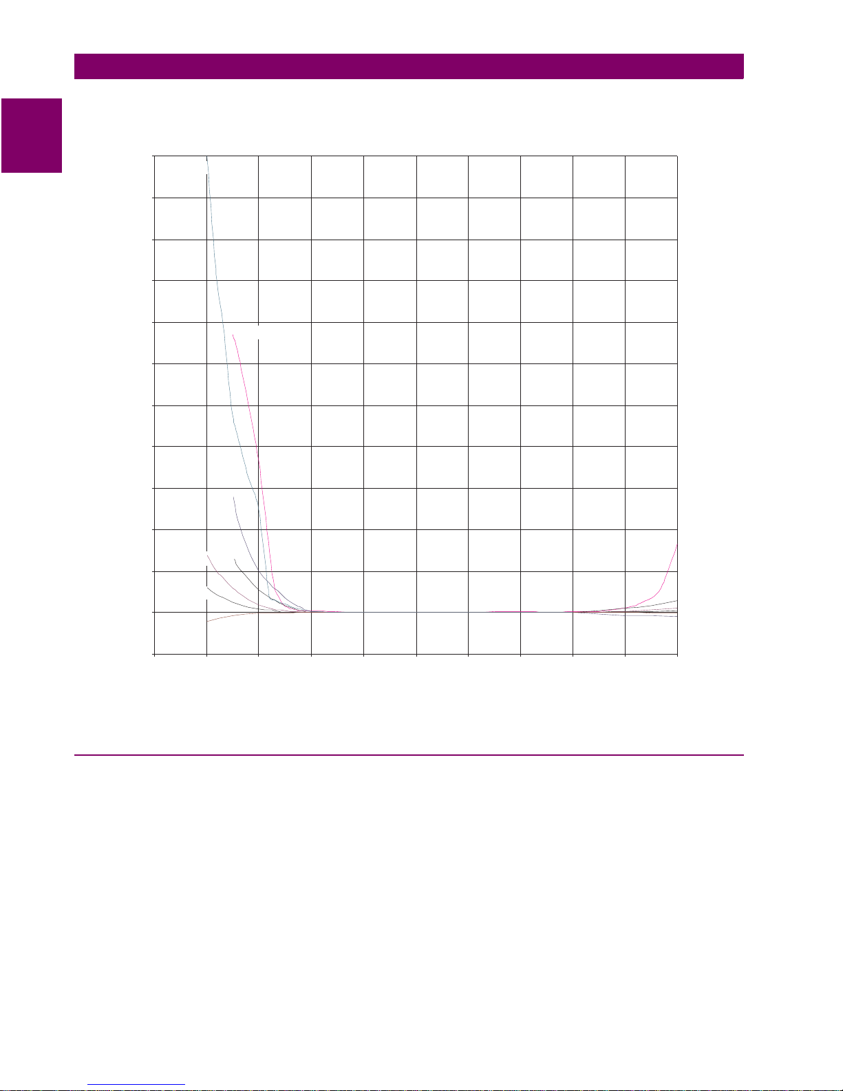
1.4.5 ADAPTIVE SAMPLING FREQUENCY
The DGP system samples analog input waveforms at a rate of 12 samples per cycle. An adaptive sampling frequency is used to m aintain th is rate ov er the power system fr equencies of 30.5 to 7 9.5 Hz. As a resu lt of this
feature, the measurem ent accuracy of the analog inp uts and the sensitivities of t he protection functions ar e
maintained over the ran ge of power system frequenci es. This feature provid es improved protection for fau lts
during off-normal frequenci es (such as start-up conditions). Figure 1–8: FREQUENCY-SENS ITIVITY CHARACTERISTICS shows variations in sensitivity of protection functions at different power system frequencies.
The sampling frequency is bas ed on 30.5 Hz for powe r system frequencies below 30.5 Hz and 79.5 Hz for the
frequencies above 79.5 Hz. In eit her case, i f the AC v oltage to the DGP drops below approx imately 20 V, the
sampling freque ncy is automati cally reca lculated on the basis of the nominal system frequency (S etting 102:
SYSFREQ
).
1
The sampling fr equency, which is 12 times the meas ured system freque ncy, can be accessed as one of the
Present Values.
1.4.6 TRIP CIRCUIT MONITOR
The trip circuit m onitor c onsis ts of D C vol tage an d curr ent mon itors ( TVM a nd TC M respe ctiv ely). E ach o f the
trip contacts shown with polarity marks in the elementary diagrams (see Section 1.5: ELEMENTARY DIAGRAMS) is monitored. TVM and TCM can be selectively disabled for each of the trip circuits.
Under normal conditions, DC vo ltage ac ross each of the contac ts is conti nuous ly monitored . If the DC voltag e
becomes virtually zero, then the trip circuit has "failed open". The TVM is active only when the generator is online, as indicated by th e i nput DI1. Th is function is intended to r ep lac e t he i ndi ca tin g l igh t typi ca ll y u se d for tri p
circuit monitoring. It is universally r ated for 48 through 2 50 V DC. A non-crit ical alarm is ge nerated when the
TVM detects an abnormality.
When the DGP system issues a trip, DC current through each of the appropriate trip contacts is monitored. The
trip relay is sealed -in, a s l ong as the cur r ent is flo win g, to pr ote ct th e contact. A minimum current o f 15 0 mA is
required for the TCM to recognize the trip current. Status of the trip current flow following issuance of any trip is
logged in the sequence of events.
1.4.7 SEQUENCE OF EVENTS
This function time -tags an d stor es the l ast 1 00 ev ents in m emory. The resolution of th e time -tagging is 1 mill isecond. The event list conta ins power sy stem events , opera tor actions, and se lf-te st alarms . The sequenc e of
events can be accessed, either locally or remotely, by a PC via one of the RS232 ports. A full description of this
function is contained in the Chapter 8: INTERFACE.
GE Power Management DGP Digital Generator Protection System 1-
19
Page 22
1.4 OTHER FEATURES 1 PRODUCT DESCRIPTION
1
12
11
10
9
8
7
6
Relative Sensitivity
5
4
Frequency Vs Sensitivity
DGP Relay System
64G1
32
24
3
46
2
1
0
59
51V
87G
0 102030405060708090100
System Frequency
32
46
24
Figure 1–8: FREQUENCY-SENSITIVITY CHARACTERISTICS
1.4.8 TIME SYNCHRONIZATION
The DGP system includes a real time clock that can run freely or be synchronized from an external signal. Two
different external time-sync signals are possible. If the DGP is connected to the host computer of a G-NET substation information and contr o l s yste m, then th e DG P rec ei ves a ti me-s yn c puls e v ia pi n 2 5 o f p or t P L-1. If the
DGP is not connected to a G-NET host computer, then a demodulated IRIG-B signal connected to optional port
PL-3 may be used to sy nchroni ze the clock. In bo th cases , the cl ock i n a given DG P is synch ronized to withi n
±1 mill is ec o nd of any o t he r di g it a l re lay cl ock, provided the two relays a re wi re d t o th e sa m e sy nc hr on iz in g s ig nal.
1-
20
DGP Digital Generator Protection System GE Power Management
Page 23

1 PRODUCT DESCRIPTION 1.4 OTHER FEATURES
1.4.9 FAULT REPORT & OSCILLOGRAPHY DATA
A fault report is initiated by any one of the protection-function pickup flags or an optional external oscillography
trigger input, DI5. For the fault report to be completed and stored, the DGP either has to issue a trip or the DI5
input contact must close any tim e during the fault report period. The fau lt report period begins when the firs t
protection function fla g is up or the DI5 in put co ntact is c losed. It end s when the DGP is sues a trip or when i t
has captured the selected number of post-fault waveform cycles, whichever is later. If all the pickup flags reset
without issuing a trip and the DI5 does not close, the fault report initiated by the protection flag will not be completed or stored.
The fault report includes the Unit ID, date and time, system operating time, pre-fault metering values, fault currents and voltages, trip/fa ult types, and up to 14 s equence-of-even t points logged after init iation. The system
operating time (OP TIME) is the time difference between the first prote ction function pickup flag and the first
protection function tri p. The DG P st ores the last three f ault repo rts i n its memory. A full description of the fault
report is contained in Chapter 8: INTERFACE.
DGP models with oscillography data capture capability will store waveform data in their memory each time the
system stores a fault report. A total of 120 cycles of data can be stored. The 120 cycles in memory are divided
in one, two, or three pa rtitions , bas ed on Setti ng 111:
fault can be set up to 20 cycles. It should be noted that the pre-fault cycles are based on the first flag or DI5 to
initiate the data capture.
Oscillography data in cludes station and generator identificat ion, a complete list of settings, the fault report,
internal flags, and a se lected number of pre-fault and post-fault wavef orm cycles. This data can be displa yed
using the GE-Link software program. See Chapter 10: GE-LINK SOFTWARE for details.
NUM FLTS
. The number of prefa ult cyc les cap tured per
1.4.10 LOCAL MAN-MACHINE INTERFACE
1
A local man-machine inte rf ace (M MI) , inc or porati ng a key pa d, LE D di splay, and 19 target LEDs, is pro vided to
allow the user to enter settin gs, display pres ent values, view fault ta rget informati on, and access sto red data.
The use and functioning of the MMI is fully described in the Chapter 8: INTERFACE.
1.4.11 LOCAL PRINTER
An optional printer port (PL- 2) on the rear of th e DGP permits the us e of a serial printe r. The port can also be
used to connect the DEC1000 Contact Expansion Unit (DGP***ACA models only) which provides eleven additional output relay s. The sequence-of-even ts (SOE) data are avai lable at this port for immediate printing as
they occur. Additionally, for DGP***AAA models, a variety of inform ation stored in the DGP system memo ry
can be printed when requested via the local MMI; see Chapter 8: INTERFACE for details.
GE Power Management DGP Digital Generator Protection System 1-
21
Page 24

1.4 OTHER FEATURES 1 PRODUCT DESCRIPTION
1.4.12 REMOTE COMMUNICATIONS
1
Two RS232 serial ports permit the u ser to communicate with the DGP from a n IBM PC- compatibl e compute r.
One of the ports, a DB-25 (PL-1), is located on th e rear of the case an d the othe r, a DB-9 (COMM), is located
on the front plate of the MMI module.
A PC may be connecte d to the DGP with a proper null-modem cable, provided the cable length does not
exceed 50 feet. The PC can also be connected via interposing modems if it is physically remote from the DGP.
GE-Link software is required to communicate with the DGP. The capabilities and use of the software are
described in Chapter 10: GE-LINK SOFTWARE. Refer to Chapter 9: COMMUNICATIONS for details regarding
the required cables and proper connection.
When a connection to the ho st computer of a stati on integratio n system is desi red, the following two ph ysical
connectio ns are possible:
• Standard hard-wire cables may be used for distances up to 50 feet.
• For longer distances it is possible to add an optional external adapter that plugs into PL-1 to provide a fiber
optic link between the DGP and the host computer. An isolated 5 V DC supply is internally connected to pin
11 of PL-1 to power this external adapter.
Cables and associate d equipment can be connected to each port si multaneousl y. However, when one port is
active the other is effectively disabled. For instance, when PL-1 is connected to host computer of an integration
system, it is not possible to log into the DGP from the front port when the integration system is active. If PL-1 is
connected to a modem and the front port is connected to a PC usi ng a null-modem cable, then th e first port
that becomes active is given preference, and the other port is disabled until the first is released.
1.4.13 REMOTE CONTROL
By using the local MMI or a remote PC connected to the RS232 port, it is possible to selectively operate any of
the four trip output relays fo r remote control. The control actio n may include shutdown of the mac hine, field
breaker trip, main g enerator brea ker trip, turbine trip, etc., depending on the equ ipment c onnected to the outputs. The controls descr ibed above are enabled or disabled by a ha rd-wired ju mper loca ted on the MMI module (see Figure 3–4: DGP MMI MODUL E on page 3– 5). As shi pped from the f actory, this jumper is physic ally
present and the Remote Control is disabled. To enable Remote Control, the jumper must be removed.
1.4.14 PASSWORD PROTECTION
Passwords provide sec urity when using the lo cal int erface (MMI) or duri ng remote commun ication s while running the GE-Link program. Two different passwords provide local MMI security for:
1. control operations (close trip-output contacts)
2. settings changes.
Three different passwords in the GE-Link program provide remote communications security for:
1. view and upload information
2. control operations
3. settings changes
Refer to the Chapter 8: INTERFACE for a descripti on of MMI password usag e, and refer to Chapter 10 : GELINK SOFTWARE for a description of GE-Link password usage.
The RS232 serial ports can be used with an optional RS485 to RS232 converter. Refer to Chapter 9: COMMUNICATIONS for further information on Modbus communication.
1-
22
DGP Digital Generator Protection System GE Power Management
1.4.15 REMOTE COMMUNICATIONS – MODBUS PROTOCOL
Page 25

1 PRODUCT DESCRIPTION 1.5 ELEMENTARY DIAGRAMS
1.5 ELEMENTARY DIAGRAMS
1
Figure 1–9: ELEMENTARY DIAGRAM WITH TEST BLOCKS, WYE VTs
GE Power Management DGP Digital Generator Protection System 1-
23
Page 26

1
1.5 ELEMENTARY DIAGRAMS 1 PRODUCT DESCRIPTION
Figure 1–10: ELEMENTARY DIAGRAM WITH TEST BLOCKS, DELTA VTs
1-
24
DGP Digital Generator Protection System GE Power Management
Page 27

1 PRODUCT DESCRIPTION 1.5 ELEMENTARY DIAGRAMS
1
Figure 1–11: ELEMENTARY DIAGRAM WITHOUT TEST BLOCKS, WYE VTs
GE Power Management DGP Digital Generator Protection System 1-
25
Page 28

1
1.5 ELEMENTARY DIAGRAMS 1 PRODUCT DESCRIPTION
Figure 1–12: ELEMENTARY DIAGRAM WITHOUT TEST BLOCKS, DELTA VTs
1-
26
DGP Digital Generator Protection System GE Power Management
Page 29

1 PRODUCT DESCRIPTION 1.5 ELEMENTARY DIAGRAMS
1
0286A2925ASH1.DWG
Figure 1–13: DIGITAL RELAY SYMBOL LEGEND
GE Power Management DGP Digital Generator Protection System 1-
0286A4911 SH9.DWG
27
Page 30

9 COMMUNICATIONS 9.1 INTRODUCTION
9 COMMUNICATIONS 9.1 INTRODUCTION 9.1.1 HARDWARE JUMPERS
There are two factory-ins talled hardware jumpers in the M MI module set to inhibit the ability to per form the
Remote Manual Trip function, the Remote Change S ettings function, the Remote Disable Outputs function ,
and the Remote Enable Outputs function. These hardware jumpers
tions are to be allowed (see Figure 3–4: DGP MMI MODULE on page 3–5 for details).
When establishing com munication betwe en the DGP and a remo te PC, two modems conn ected via a phon e
line are required. One modem is located at the DGP and the other modem is located at the PC. The cable that
connects the modem s with the DGP and PC is sh own in Figure 9–1: DGP CO MMUNICATIONS WIRING on
page 9–3. Each of these modems must be "Hayes-compatible". This is necessary since the GE-Link communications software send s a Hayes-com patible command string to the PC modem. The DGP do es not send any
configuration comm ands to i ts modem . The DGP modem and the PC modem mu st be uni quely con figured t o
permit the user to log into and communicate with the DGP system with GE-Link.
The required configuration settings are presented as changes to the factory-default configuration settings for a
Hayes SmartModem. These default settings are:
B1 P Y0 &K3 &S0 S7=30 S11=95 S26=1
E1 Q0 &C0 &L0 &T4 S8=2 S12=50 S36=1
L2 V1 &D0 &P0 &X0 S9=6 S18=0 S37=0
M1 W0 &G0 &Q5 S0=0 S10=14 S25=5 S38=20
N1 X4 &J0 &R0 S6=2
must
be removed if the above remote func-
9.1.2 MODEM CONNECTIONS & SETTINGS
Other Hayes-compatible modems may implement a subset of the full Hayes command set. It is the responsibility of the user to as certa in the ex act co mma nds a cc ept ed b y a pa rtic ula r mod em. The p ro per syn tax for e ntering the Hayes-compatible commands (s ome times referred to as the "AT" command set) is not des c ribe d he re.
Refer to the modem documentation for an explanation of this syntax.
9.1.3 PC MODEM
The PC modem must be configured for intelligent operation (that is, command recognition enabled). The
default settings li sted abo ve ar e vali d for GE-L ink. T hose conf igu ratio n setti ngs cri tical to the oper ation of GELink are changed by the software. The configuration commands sent to the modem from GE-Link are:
+++
ATE0L3Q0S7=60V0X4Y0
Command explanation:
AT Modem attention command
E0 Disable command state echo
L0 Low speaker volume
Q0 Modem returns result codes
V0 Result codes returned in numeric form
X4 Enables features represented by result codes
Y0 Disable long space disconnect
S7=60 Allows modem to hang up if connection is not made within 60 seconds
(set modem to command mode)
(delay 2 seconds)
(see explanation below)
9
GE Power Management DGP Digital Generator Protection System 9-
1
Page 31

9.1 INTRODUCTION 9 COMMUNICATIONS
If all of the above c ommands ar e not program mable, the mo dem may not operate proper ly. In addition to the
required configuration settings above, it is suggested that two other settings be made. These are:
&D3 Causes the modem to reset on the ON-to-OFF transition of DTR (Data Terminal Ready)
&C1 Causes DCD (Data Carrier Detect ) to track the received carrier signal
The modem will ope rate properly without making these tw o settings but the modem will n ot hang up if the
appropriate handshaking signal is lost.
A GE-Link setting establi shes the baud rate, whi ch m ust matc h the DGP baud rate s etting. GE-L ink then sets
the specified PC s erial port (i.e., COM1 , COM2) to the proper baud rate , parity, data bits, and stop b its. If the
PC modem is capable of operating at more than one baud rate, then it must be able to automatically configure
its baud rate, character length, and parity setting by examining the AT command prefix.
9.1.4 DGP MODEM
The DGP modem must be configured for "dumb " opera tion (tha t is, command recogniti on disa bled) . Since the
DGP does not send any co nfiguration commands to its modem , the required configuration setti ngs must be
made prior to connecti on. Additionally, the modem must be initialized to the required con figuration settings
each time modem power is turned OFF then ON. Depending on the design of the modem, this is accomplished
by making the required settings via switches or saving the settings in non-volatile memory.
The required configuration settings are:
E0 Disable command state echo
L0 Low speaker volume
Q1 Disable result code display
&C1 Causes DCD (Data Carrier Detect) to track the received carrier signal
&D3 Causes the modem to reset on the ON-to-OFF transition of DTR (Data Terminal Ready)
&Q0 Asynchronous mode
S0=1 Enable auto-answer
If any of the above se ttings cannot be implemen ted, the modem may not ans wer, the DGP system may not
connect properly, or the user may not be able to log into the DGP.
With a Hayes SmartModem or equivalent, the DGP modem pe rforms a modulation handshake with t he PC
modem to set the DGP modem baud rate. The default setting N1 permits ha ndshaking to occur at any bau d
rate supported by both modems. This is one reason why it is preferable to use identical modems at each end.
Note that auto-answering is contr olled with register S0. S0=0 disables auto-an swer. S0=1 causes the DGP
modem to answer the in coming c all after one r ing. If it is de sirabl e to delay mo dem answeri ng, S0 can b e set
for any value between 1 and 255 (for the Hayes-compatible modem assumed). Note that GE-Link (versions 2.0
and higher) configur es the PC mod em to wait 60 se conds for the DGP modem to answer. If the DGP modem
register S0 is set higher than 12, the PC modem may time-out and hang up before the DGP modem can
answer. S0=12 sets the DGP modem to answer after twelve rings, corresponding to an approximate 60 second
delay (S7=60) at the PC mode m. However, the number of rings corr esponding to 60 sec onds should be v erified for a particular application.
9.1.5 NULL MODEM CONNECTIONS
9
A PC can be connected to the DGP with out the intervenin g modems a nd phone l ine by usin g a "null mod em"
cable. The required pin-to-pi n connec tions for this null modem cab le are shown in the following diagra m. The
pin-to-pin connection s for a null modem ca ble to DGP COMM connecto r are also shown below. Neither null
modem cable should exceed 50 feet in length.
9-
2
DGP Digital Generator Protection System GE Power Management
Page 32

9 COMMUNICATIONS 9.1 INTRODUCTION
TO RELAY
PL-2
TO RELAY
PL-1
25 PIN D-TYPE
MALE
TD
RD
CTS
GND
TD
RD
RTS
CTS
DSR
GND
DCD
DTR
RI
2
3
5
7
A) PRINTER CONNECTIONS
25 PIN D-TYPE
MALE
2
3
4
5
6
7
8
20
22
B) REMOTE COMMUNICATIONS VIA MODEM CABLE
25 PIN D-TYPE
MALE / FEMALE
TD
2
RD
3
GND
7
DTR
20
25 PIN D-TYPE
MALE / FEMALE
2
TD
3
RD
4
RTS
5
CTS
6
DSR
7
GND
8
DCD
20
DTR
22
TO
PRINTER
TO
MODEM
RI
TO RELAY
PL-1
TO RELAY
MMI MODULE
COMM
25 PIN D-TYPE
MALE
TD
RD
RTS
CTS
DCD
DSR
RI
DTR
GND
TD
RD
DSR
RI
DTR
RTS
CTS
DCD
GND
2
3
4
5
8
6
22
20
7
C) REMOTE COMMUNICATIONS TO PC DIRECTLY
9 PIN D-TYPE
MALE
3
2
6
9
4
7
8
1
5
D) REMOTE COMMUNICATIONS FROM MMI MODULE TO PC
25 PIN D-TYPE
MALE / FEMALE
TD
2
RD
3
RTS
4
CTS
5
DCD
8
DSR
6
22
DTR
20
GND
7
9 PIN D-TYPE
MALE / FEMALE
TD
3
RD
2
DSR
6
RI
9
DTR
4
RTS
7
CTS
8
DCD
1
GND
5
TO
PC
RI
TO
PC
9
CABLES AVAILABLE AS GE PART NO. 0246A9866. SPECIFY CABLE TYPE AND CONNECTOR GENDER.
GE Power Management DGP Digital Generator Protection System 9-
Figure 9–1: DGP COMMUNICATIONS WIRING
3
Page 33

9.1 INTRODUCTION 9 COMMUNICATIONS
9.1.6 RS485 COMMUNICATIONS
The DGP with Modbus comm unications can be used with a G E Power Management RS485 to RS23 2 converter when necessary. For computers without RS485 capabi lity, a “master” SCI box is required as shown in
the figure below. The SCI boxes are available from GE Power Management as catalog number S14200
where
X
specifies the voltage input. Please consult the SCI documentation for additional configuration informa-
tion.
X
,
For RS485 communications, the Master SCI box switch #2 must be set for
default) and the Slave switch #2 must be set for
NOTE
Correct polarity is also ess en tia l. A LL wi res fro m the Mas ter SCI to the Slave SCI must be wired wi th the pos itive (+) terminal s connected together and th e negative (–) terminals con nected together. Each relay must be
daisy-chained to the next. Avoid sta r or stub conne cted confi gurations. The last device ( SCI box) at each en d
of the daisy-chain should be terminate d with a 12 0 Ω, ¼ W resistor in series with a 1 nF capacitor across the
positive (+) and negative (–) terminal s.
Table 9–1: SCI DIP SWITCH CONFIGURATION
SWITCH 1 1234
Data Controlled ON OFF ON X
DTR Controlled OFF ON OFF X
SWITCH 2 1234
Direct ON OFF ON OFF
Modem OFF ON OFF ON
MODEM
. Set switch #1 for
DIRECT
DATA CONTROLLED
(the factory
.
9
Figure 9–2: RS485 COMMUNICATIONS
9-
4
DGP Digital Generator Protection System GE Power Management
Page 34

9 COMMUNICATIONS 9.2 MODBUS COMMUNICATIONS
9.2 MODBUS COMMUNICATIONS 9.2.1 INTRODUCTION
This section describe s the Mod icon Modbus RTU comm unicati on prot ocol use d by the DGP Digita l Gene rator
Protection Relay.
The device serial communi cation parameter s, such as baud rate an d DGP Unit ID, are set via the keypad. If
the DGP baud rate differs from the Modbus server baud rate , the device will not comm unicate to the server.
The Unit ID also must be set properly to avoid confli ct with other devices connected on the same network.
Even though the setti ng range allow s 16 bit va lues for Unit ID, the relay s hould be pr ogrammed for a Unit ID
ranging from 1 to 127.
The DGP impleme nts a subset of protocols defined b y the Modicon Modbus RTU p rotocol standar d. Multiple
DGP relays can be c onfigu red as s laves t o a si ngle Modb us mas ter thr ough th e RS485 port (u sing an RS48 5
to RS232 converter ). The DGP is alway s a slave – it cann ot be programmed as a master. Even though the
Modbus protocol is availa ble in Modbus RTU, Modbus ASCII and Modb us Plus protocols, only the Modbus
RTU protocol is supported by the DGP.
9.2.2 DATA FRAME FORMAT & DATA RATE
One data frame of asynchr onous transmission fro m the DGP is defaulted to 1 start bit, 8 data bits, no p arity
bits, and 1 stop bit at 96 00 baud. The b aud rate, parity bi ts and number o f stop bits can b e changed thr ough
the DGP keypad. This setting cannot be changed through the Modbus COM port.
9.2.3 DATA PACKET FORMAT
A complete request/response sequence consists of the following bytes.
Modbus Request Transmission: Bytes
SLAVE ADDRESS 1
FUNCTION CODE 1
DATA STARTING ADDRESS 2
DATA variable number depending on function code
REGISTER CODE 2 bytes
CRC Hi High byte of CRC
CRC Lo Low byte of CRC
Slave Response Transmission: Bytes
SLAVE ADDRESS 1
FUNCTION CODE 1
BYTE COUNT variable depending on number of registers
DATA variable number depending on the function
CRC Hi High Byte of CRC
CRC Lo Low byte of CRC
a) SLAVE ADDRESS
9
This is the first byte of every transmission. It represents the Unit ID of the device programmed through the DGP
keypad. In the master request, the slave address represents the address of the slave the message is intended
for. In the slave response it is the address of the slave that is responding to the master request. Slave address
0 is reserved for broadcas t transm issions by the m aster as s pecifi ed by the Modbus protocol. The DGP d oes
not support the broadcast transmissions. The DGP will respond only if the slave address specified by the master request matches its Unit ID; otherwise the DGP relay will not respond.
GE Power Management DGP Digital Generator Protection System 9-
5
Page 35

9.2 MODBUS COMMUNICATIONS 9 COMMUNICATIONS
b) FUNCTION CODE
This is the second byte of every transmission. Modbus defines function codes 1 to 127 but the DGP impl ements only a subset of these functions. In a master request, the function code represents the action to be performed by the slave. The slav e resp onds wi th function c ode ide ntica l to that se nt by the ma ster if ther e are no
errors. In case of an error or exception, the slave sets the MS bit of the function code to 1 to indicate an error.
c) DATA
This will be a variable number of bytes depending on the function code.
d) CRC HI & CRC LO
This is a two-byte cycl ic redun dancy check . The MS by te is sent fi rst and th e LS by te next in accor danc e with
the Modbus protocol reference guide.
9.2.4 ERROR CHECKING
In RTU mode, messages i nclude an error checking fiel d that is ba sed on a cy clic redundan cy check me thod.
The CRC field checks the contents of the entire me ssage. It is appli ed regardless of any parity check method
used for the individual characters of the message.
The CRC field is two byte s, containing a 1 6-bit binar y value. The CRC value is ca lculated by the t ransmittin g
device, which appends the CRC to the me ssage. The receiving device recalc ulates CRC and compares with
the value it received in the CRC field. If they are not equal an error message results.
The CRC is calculated by fi rst pre-loading a 16-bit register to al l 1’s (in GE relays, all registers are pre-loade d
with zeros). Then using a CRC polynomial specified by the CCITT, the CRC is computed (0xA001).
9.2.5 DATA FRAMING
Modbus RTU messages are s eparated by a silence period of at least 3.5 characters. The sl ave flushes the
COM port and reads for th e f irst c harac ter. This marks th e s tart of tra nsmi ssio n. Th e sl av e k ee ps r ead ing un til
a silent interval of 3.5 c haracter s which is abou t 3.65 ms at 9600 baud, wh ich marks the end of tra nsmission .
At this stage it builds the message and resets the port.
9
9-
6
DGP Digital Generator Protection System GE Power Management
Page 36

9 COMMUNICATIONS 9.3 MODBUS FUNCTIONS
9.3 MODBUS FUNCTIONS 9.3.1 FUNCTION CODE 03/04: READING HOLDING/INPUT REGISTERS
a) DESCRIPTION
Reads the binary c ontents ho lding/in put regi sters (ac tual va lues) in the sl ave. They can be s et point registers
or any of the information reports, such as actual values.
b) QUERY
The query message specifies the starting register and the number of registers to be read.
Field: Bytes Example (hex):
SLAVE ADDRESS 1 11 Message for slave 17
FUNCTION CODE 1 03/04 Read registers
Starting address 2 Starting address of the register. High byte first and then the Low Byte
Num points 2 Number of registers to read. High Byte first then Low byte
CRC 2 CRC Calculated by master. High byte first. Low byte next
c) RESPONSE
The register data i n the r espo nse i s packe d as two by tes per registe r. For each register t he fir st byte co ntains
the higher order byte and the second contains the lower order byte.
Example of typical response message
Field: Bytes Example (hex):
SLAVE ADDRESS 1 11 Message from slave 17
FUNCTION CODE 1 03/04 Read registers
Byte Count 1 Number of registers to read.
Data 1 2 High Byte first then Low byte
......
Data n 2 High Byte first then Low byte
CRC 2 CRC calculated by slave. High byte first, Low byte next
9
GE Power Management DGP Digital Generator Protection System 9-
7
Page 37

9.3 MODBUS FUNCTIONS 9 COMMUNICATIONS
9.3.2 FUNCTION CODE 05: FORCE SINGLE COIL
a) DESCRIPTION
This function code allows the master to request a DGP slave to perform a specific command operation.
b) QUERY
The query message specifies the command to be executed.
Field: Bytes Example (hex):
SLAVE ADDRESS 1 11 Message for slave 17
FUNCTION CODE 1 05 Execute a command
Coil address 2 Starting address of the command to be executed. High byte first and
then the Low Byte
Value 2 FF00 perform function
CRC 2 CRC Calculated by master. High byte first. Low byte next
c) RESPONSE
The normal resp onse is an echo of the query returned after the command h as been executed. Example of
response to function 05H
Field: Bytes Example (hex):
SLAVE ADDRESS 1 11 Message from slave 17
FUNCTION CODE 1 05 Execute a coil command
Coil Address 2 Address of the command that has been executed
Value 2 FF00 Same as the master query
CRC 2 CRC Calculated by Slave High byte first. Low byte next
9
9-
8
DGP Digital Generator Protection System GE Power Management
Page 38

9 COMMUNICATIONS 9.3 MODBUS FUNCTIONS
9.3.3 FUNCTION CODE 06: STORE SINGLE SETPOINT
a) DESCRIPTION
This function code allow s the master to p reset a DGP setpo int or to write to some control registers dur ing the
report reads.
b) QUERY
The query message specifies the setpoint to be preset
Field: Bytes Example (hex):
SLAVE ADDRESS 1 11 Message for slave 17
FUNCTION CODE 1 06 Store a single setpoint
Register address 2 Address of the register to be preset
Value 2 Valu e of the set point re gis ter
CRC 2 CRC Calculated by master. High byte first. Low byte next
c) RESPONSE
The normal response i s an echo of the query returned after the content s of the register have been preset.
Example of response to function 06H.
Field: Bytes Example (hex):
SLAVE ADDRESS 1 11 Message from slave 17
FUNCTION CODE 1 06 Store a single setpoint
Register Address 2 Address of the register that has been set to the value specified by the
Master
Value 2 Same as the value specified by the master query.
CRC 2 CRC Calculated by Slave High byte first. Low byte next
9
GE Power Management DGP Digital Generator Protection System 9-
9
Page 39

9.3 MODBUS FUNCTIONS 9 COMMUNICATIONS
9.3.4 FUNCTION CODE 16: PRESET MULTIPLE SETPOINTS
a) DESCRIPTION
This function code allows the master to preset Multiple Setpoint registers of the DGP Slave.
b) QUERY
The query message specifies the registers to be preset.
Field: Bytes Example (hex):
SLAVE ADDRESS 1 11 Message for slave 17
FUNCTION CODE 1 10 Store setpoints
Starting Address 2 Starting address of the register to be preset
Number of registers 2 Number of set point registers
Byte Count 1 Number of bytes. Equal to twice the number specified by the Number
of registers
Data1 2 Set point Value 1
.....
Data n 2 Set point value of the nth register from starting register
CRC 2 CRC Calculated by master. High byte first. Low byte next
c) RESPONSE
The normal response retur ns the slave ad dress the func tion ID, Starti ng Address an d the number of registers
preset. An example is given below.
Field: Bytes Example (hex):
SLAVE ADDRESS 1 11 Message from slave 17
FUNCTION CODE 1 10 Store setpoints
Starting Address 2 Starting address of the register to be preset
Number of registers 2 Number of set point registers
CRC 2 CRC Calculated by master. High byte first. Low byte next
9.3.5 FUNCTION CODE 56: RETRANSMIT LAST PACKET
a) DESCRIPTION
This function is not supported by the Modbus protocol as it is a GE specific enhancement. When this command
is issued, the last response from the slave is simply repeated.
b) QUERY
Example of a query message.
Field: Bytes: Example (hex):
SLAVE ADDRESS 1 11 Message for slave 17
9
FUNCTION CODE 1 38 Retransmit last packet
CRC 2 CRC Calculated by Slave High byte first. Low byte next
c) RESPONSE
The DGP Slave responds with the last message it transmitted to the master.
9-
10
DGP Digital Generator Protection System GE Power Management
Page 40

9 COMMUNICATIONS 9.4 MODBUS ERRORS
9.4 MODBUS ERRORS 9.4.1 ERROR RESPONSES
When a DGP slave detec ts an err or a res ponse will be sen t to the mas ter. The MSBit of the functio n code wi ll
be set to 1 and the following byte is an exception code.
The Slave response will be
Field: Bytes Example (hex):
SLAVE ADDRESS 1 11 Message from slave 17
FUNCTION CODE 1 Function ID with MSbit set to 1
Exception Code 1 Exception Code
CRC 2 CRC Calculated by Slave High byte first. Low byte next
The DGP will implement the following exception response codes.
01: Illegal function
02: Illegal Data Value
03: Illegal Data Address
GE Power Management DGP Digital Generator Protection System 9-
9
11
Page 41

9.5 MODBUS MEMORY MAPPING 9 COMMUNICATIONS
9.5 MODBUS MEMORY MAPPING 9.5.1 DATA TYPES
The DGP implementati on of Modbus uses a sm all set of data types to interpret the data i n the relay. Unless
otherwise noted, all the data will be communicated with the MS byte first and then the LS bytes.
The following data types will be used by the DGP modbus communication.
ASCII
1.
2.
3.
4.
5.
: Each register is an AS CII character, with the high byte always zero and the low by te representin g
the ASCII character.
DT0
: The date and time in seven registers. The registers have the following format:
Register 1 – day range 1 to 31
Register 2 – month range 1 to 12
Register 3 – year range 00 to 99
Register 4 – hour range 0 to 23
Register 5 – minutes range 0 to 59
Register 6 – seconds range 0 to 59
Register 7 – milliseconds range 0 to 999.
DT1
: Six registers with the same format as DT0 except without the millisecond field.
LONG0
LONG1
: Two registers. Byte order – Byte3 Byte2 Byte1 Byte0. No implied decimal point.
: Two registers. Byte order – Byte3 Byte2 Byte1 Byte0. One implied decimal place.
For example, 3.4 will be represented as long integer 34.
LONG2
6.
INT0
7.
INT1
8.
INT2
9.
BOOLEAN
10.
SOE
11.
ister 8 is the event code (see DGP event code list below). If the requested event contains no data, then all
8 registers contain a value of 0.
12.SP: Special processing needed. Most of the registers are bit fields..
: Two registers. Byte order – Byte3 Byte2 Byte1 Byte0. One implied decimal place.
For example, 3.45 will be represented as long integer 345.
: One register. Byte order – Byte2 Byte1. No implied decimal place, integer value on ly.
: One register. Byte order – Byte2 Byte1. One implied decimal place.
For example, 3.4 will be represented as 16-bit integer 34.
: One register. Byte order – Byte2 Byte1. Two implied decimal places.
For example, 3.45 will be represented as 16-bit integer 345.
: High byte is always 0; low byte is either 0 or 1.
: Eight registers. The first se ve n re gist e rs co rres po nd to dat e and ti me ac cor din g to for ma t DT0 . Reg-
9
9-
12
DGP Digital Generator Protection System GE Power Management
Page 42

9 COMMUNICATIONS 9.5 MODBUS MEMORY MAPPING
9.5.2 MEMORY MAP ORGANIZATION
The register maps have been designed by function basis as for GE-Modem to faci litate ease of desi gn. For
example, the Set Date and Time function is implemented by writ ing to certain setpoint reg ist ers ev en t hou gh i t
is not a part of the actual setting s gr oup. Se ttings ar e den oted by the r egister addres ses with the most s ignif icant two bits represe nting 01B . Reports ar e represent ed by addresses wi th most significan t two bits having a
value of 00B. However, there are some control registers with in the report register map and they are read/write
registers for setting the appropriate registers. They are programmed by Function 06.
Table 9–2: MEMORY MAP ORGANIZATION
MEMORY MAP SECTION ADDRESS RANGE DESCRIPTION
Fixed Value Input Registers 0000 to 001BH PROM version and other model details
Present Value Report
Registers
Event Report Register Map 0800 to 0B20H The last 100 events
Fault Status Register Map 0C00 to 0C18H Faults 1 to 3 header
Fault Report Register Map 1000 to 129DH Fault Report Summary for up to 3 faults
Oscillography 1400 to 17FFH Oscillography header, settings, and data
DGP Status Register Map 1800 to 180CH DGP status and self-test diagnostics
MMI Passwords 1C00 to 1C1FH Passwords
Settings 4000 to 5D05H DGP relay protection settings
Station and Generator ID 7E00 to 7E1FH Station and Generator IDs
Range: 0000 to 001BH
The fixed value registers contain the PROM version number and other details which do not normally change in
the field. These registers are read only registers and read by Function Codes03/04.
0400 to 0431H DGP Present Values
9.5.3 FIXED VALUE INPUT REGISTERS
9.5.4 PRESENT VALUE REPORT REGISTER MAP
Range: 0400 to 0431H
This register map specifies the present values report. The report is read by the master by using Function Code
03/04. Any attempt to write to these read-only registers causes an ILLEGAL ADDRESS exception to be
returned.
Status Bits Representation:
Register 0438H:
bit 0 - New Event(s)
bit 1 - New Fault(s)
bit 2 - In time sync
bit 3 - Local Settings change started
bit 4 - Local Settings change Done
EVENT/FAULT FLAG
GE Power Management DGP Digital Generator Protection System 9-
9
13
Page 43

9.5 MODBUS MEMORY MAPPING 9 COMMUNICATIONS
9.5.5 EVENT REPORT MEMORY MAP
Range: 0800 to 0B20H
The event report memory map st arts with the addresses with the six most-significa nt bits set to 000010B. All
the registers are read-only; they can be read by using function codes 03 and 04.
Register 0800H must be read firs t to determi ne the numbe r of events. If a request is made fo r
more events than present, the extra events are padded with zeros to signify no event is
NOTE
Range: 0C00 to 0C18H
The fault status map has the register address with most-significant bits set to 000011B. These read-only registers are read with Modb us function c odes 03/ 04. The first reg ister cont ains the n umber of faul ts. This reg ister
must be read first to determine the number of faults. I f a request is m ade for more f aults than recorded, the
data is filled with zeros. The maximum number of faults is determined by Setting 111:
attempts to read more faults than determined by this setting, an ILLEGAL ADDRESS exception is generated.
The TRIP TYPE field is a 16 bit binary value representing the function that has tripped due to the fault. The bit
assignments are as follows:
present. Registers 0801H to 0808H always contains the latest event; registers 0B19H to 0B20H
contain the oldest events.
9.5.6 FAULT STATUS MEMORY MAP
NUM FLTS
. If the master
Registers 0C08H, 0C10H, and 0C18H:
bit 0 - 94G
bit 1 - 94G1
bit 2 - 94G2
bit 3 - 94G3
bits 4 to 15 - reserved and presently set to zero
Range: 1000 to 129DH
The fault report memory map has the register addres s with most signifi cant bits set to 00010 0B. These readonly registers are read by Modbus Function Codes 03 and 04. The first register 1000H contains the number of
faults recorded. The user must read this register first to find the number of faults. If a request is made for more
faults than recorded, the data is filled with zeros. The maximum numb er of faul ts is dete rm in ed by Sett ing 111:
NUM FLTS
exception is generated.
The fault report summ ary can stor e up to 10 s equence of eve nts, with the o ldest event rec orded in the lower
address (note that in th e event report it is th e opposite – the latest event is r ecorded in the lo wer address). If
there are fewer than 10 events, the remaining registers are filled with zeroes to signify there are no events.
The
assignments are as follows:
9
. If the master attempts to read more faults than determined by this setting, an ILLEGAL ADDRESS
TRIP TYPE
field is a 16-bit binary value representing the function that has tripped due to the fault. The bit
TRIP TYPE
9.5.7 FAULT REPORT REGISTER MAP
bit 0 - 94G
bit 1 - 94G1
bit 2 - 94G2
bit 3 - 94G3
bits 4 to 15 - reserved and presently set to zero
9-
14
DGP Digital Generator Protection System GE Power Management
Page 44

9 COMMUNICATIONS 9.5 MODBUS MEMORY MAPPING
9.5.8 OSCILLOGRAPHY REPORT MEMORY MAP
Range: 1400 to 16FBH
The oscillography report c ontains three par ts: the oscillograph y header, active settings for the partic ular fault,
and oscillography d ata. Since t he memory map is not sufficient for the enti re oscillography report, the m ap is
designed such a way that t he fa ult numb er and cycl e nu mbe r f or the os c il logr aphy in int er est are s ele cte d an d
read from a fixed set of registers. The oscillogra phy hea der an d settings are unique for ea ch faul t num ber an d
do not depend on the cycle number. The oscillography data depends both on cycle number and fault number.
All oscillography registers have an address with most significant 6 bits set to 000101B.
a) CONTROL REGISTERS
Range: 17FE to 17FFH
The control register s are wri tten using Mo dbus Fu nction Cod e 06/10. T hese register s are rea d-write re gisters
and can be read using Function Codes 03 and 04.
The fault number range is limited by Sett ing 111:
same setting. That is, fo r one fa ult the r ang e is 1 to 120, fo r two fau lts the ran ge i s 1 t o 60, a nd fo r thre e fau lts
it is 1 to 40. In addit ion, if the fault number is set higher than the number of fa ults recorded, the DGP sl ave
responds with ILLEGAL DATA VA LUE exception. The numbe r of faults recorded can be obtai ned by reading
the register 1400H.
Fault Number 1 corresponds to the newest fault and Fault number 3 corresponds to the oldest fault.
You must write the fault number to register 17FFh and the cycle number to register 17FEh
before reading the oscillography data corresponding to this fault.
NOTE
b) OSCILLOGRAPHY HEADER
Range: 0C00H to 129DH
The first register (0C000H) contains the number of faults recorded. The rest of th e registers con tain the prefault values, fault value s, and the sequence of events. In es sence, this block is identical to the fault report
header. All registers are read-only and can be read by Function Codes 03/04.
When a request is made to read these registers, the DGP relay looks at register 17FFH. If it is with in range
then it responds w ith the osci llograp hy header c orresponding to the fa ult number i n the regis ter 17FFH. If the
number is not valid, the DGP slave responds with ILLEGAL DATA VALUE exception.
c) OSCILLOGRAPHY SETTINGS
Range: 1400 to 1483H
NUM FLTS
. The cycle number range is also limited by the
Oscillography sett ings start from register 1400H. Al l registers are read-only and c an be read using function
codes 03H/04H.
When a request is made to read these registers, the DGP relay looks at register 17FFH. If it is with in the range
then it responds with th e o sc illo gr aph y se tti ngs cor r espon ding to the fault num ber put in the register 1 7FF H. If
the number is not valid the DGP slave responds with ILLEGAL DATA VALUE exception.
GE Power Management DGP Digital Generator Protection System 9-
9
15
Page 45

9.5 MODBUS MEMORY MAPPING 9 COMMUNICATIONS
d) OSCILLOGRAPHY DATA
Range: 1600H to 16FBH
Oscillography data contains 16 registers per sample with 12 samples per cycle and therefore 192 registers per
cycle of interest. Be fore r ea din g th e da ta, the master has to pro gr am control registers 17F EH w ith the cy cle o f
interest and 17FFH with the fault number.
When a request is made to read these registers, the DGP look s at registers 17FE H and 17FFH. If they are
within range, it respond s with the oscillography data corresponding to the faul t number and cycle number in
registers 17FFH and 17F EH. If these numbe rs are not valid, the n the DGP slave resp onds with an ILLEGA L
DATA VALUE exception.
All these registers are read-only registers and are read using Function Codes 03/04.
e) COMMUNICATION EXAMPLE
An example is given here to show the sequence of transactions for retrieving oscillography:
1. Read the Number of Faults at registers 1000H.
2. Select a fault and write the corresponding fault number into register 17FFH.
3. Read data from 0C00H to 1483H for the oscillography header or fault summary.
4. Read data from 1600H to 16FBH for the Active settings at the time of fault.
5. Cycle Num =1.
6. If (cycle num > Max_Num) go to step 10.
7. Write the Cycle Num into register 17FEH.
8. Read the oscillography data from registers 1600H to 16FBH.
9. Increment the Cycle Num and go to step 6.
10. Finished reading Oscillography.
9
9-
16
DGP Digital Generator Protection System GE Power Management
Page 46

9 COMMUNICATIONS 9.5 MODBUS MEMORY MAPPING
9.5.9 EVENT CODES & STATUS REGISTERS
a) EVENT CODES
A list of DGP event codes with their corresponding event messages is shown below:
0 FAIL - DAP BOARD: PROM
1 FAIL - DAP BOARD: LOCAL RAM
2 FAIL - DAP BOARD: DSPRAM CRC
3 FAIL - DAP BOARD: DSPRAM
4 FAIL - DAP BOARD: SYSRAM
5 FAIL - DAP BOARD: INTERRUPT
6 FAIL - DAP BOARD: TIMER
7 FAIL - DSP 1 BOARD: PROM
8 FAIL - DSP 1 BOARD: LOCAL RAM
9 FAIL - DSP 1 BOARD: SHARED RAM
10 FAIL - DS P 1 B OARD: NO RESPONSE
11 FAIL - ANI BOARD: CONTROLLER
12 FAIL - ANI BOARD: SERIAL MEMORY
13 FAIL - ANI BOARD: REFERENC E
14 FAIL - MGM 1 BOARD: SERIAL MEMORY
15 FAIL - SSP BOARD: PROM
16 FAIL - SSP BOARD: LOCAL RAM
17 FAIL - SSP BOARD : S YSRAM CRC
18 FAIL - SSP BOARD: SYSRAM
19 FAIL - SSP BOARD: IN TERRUPT
20 FAIL - SSP BOARD: EEPROM
21 FAIL - MMI BOARD: DIGITAL OUTPUT
22 FAIL - MGM 1 BOARD: MODEL NUMBER
23 FAIL - SSP BOARD: VERS ION NUMBER
24 FAIL - DAP BOARD: VERSION NUMBER
25 FAIL - DSP 1 BOARD: VERSION NUMBER
26 FAIL - DSP 2 BOARD: PROM
27 FAIL - DSP 2 BOARD: LOCAL RAM
28 FAIL - DSP 2 BOARD: SHARED RAM
29 FAIL - DSP 2 BOARD: NO RES P ONSE
30 FAIL - DSP 2 BOARD: VERSION NUMBER
31 FAIL - DSP 3 BOARD: PROM
32 FAIL - DSP 3 BOARD: LOCAL RAM
33 FAIL - DSP 3 BOARD: SHARED RAM
34 FAIL - DSP 3 BOARD: NO RES P ONSE
35 FAIL - DSP 3 BOARD: VERSION NUMBER
36 FAIL - ANI BOARD: GROUND REFER ENCE
37 FAIL - PS1 BOARD: LOGIC VOLTAGE FAILED
38 FAIL - PS1 BOARD: +12 VOLTAGE FAILED
39 FAIL - PS1 BOARD: -12 VOLTAGE FAILED
40 FAIL - PS2 BOARD: LOGIC VOLTAGE FAILED
41 FAIL - PS2 BOARD: +12 VOLTAGE FAILED
42 FAIL - PS2 BOARD: -12 VOLTAGE FAILED
43 FAIL - PS BOARD: LOGIC VOLTAGE FAILED
44 FAIL - PS BOARD: +12 VOLTAGE FAILED
45 FAIL - PS BOARD: -12 VOLTAGE FAILED
46 FAIL - DSP 1 BOARD: SET TING CHECKSUM
47 FAIL - DSP 2 BOARD: SET TING CHECKSUM
48 FAIL - DSP 3 BOARD: SET TING CHECKSUM
49 FAIL - MGM 2 BOARD: SERIAL MEMORY
50 FAIL - MGM 2 BOARD: MODEL NUMBER
51 FAIL - ANI BOARD:CURRENT SUM
52 FAIL - ANI BOARD:CHANNEL SATURATED
53 FAIL - SSP BOARD:SET TINGS OUT OF RANGE
54 " "
55 WARN - MMI BOARD: PRIN T SERIAL CHIP
56 WARN - SSP BO ARD: TIMER
57 WARN - SSP BOARD: CAPRAM
58 WARN - SSP BOARD: REAL TIME CLOCK
59 WARN - MMI BOARD: LE D DISPLAY
60 WARN - REMOTE COMM LOGIN FAILED
61 WARN - SPURIOUS TIME STROBES
62 WARN - DTA BOARD: SERIAL MEMORY
63 WARN - MMI BOARD: FRONT SERIAL CHIP
64 WARN - MMI BOARD: BACK SERIAL CHIP
65 WARN - PS1 BOARD: LOGIC VOLTAGE FAILED
66 WARN - PS1 BOARD: +12 VOLTAGE FAILED
67 WARN - PS1 BOARD: -12 VOLTAGE FAILED
68 WARN - PS2 BOARD: LOGIC VOLTAGE FAILED
69 WARN - PS2 BOARD: +12 VOLTAGE FAILED
70 WARN - PS2 BOARD: -12 VOLTAGE FAILED
71 WARN - CASE TO GROUND SHORTED
72 WARN - DIT BOARD: DIGITAL INPUT FAIL
73 WARN - ANI BOARD: SAMPLE CORRECTED
74 " "
75 " "
76 32-2 ON
77 32-2 OFF
78 51V PHASE A ON
79 51V PHASE B ON
80 51V PHASE C ON
81 51V PHASE A OFF
9
GE Power Management DGP Digital Generator Protection System 9-
17
Page 47

9.5 MODBUS MEMORY MAPPING 9 COMMUNICATIONS
82 51V PHASE B OFF
83 51V PHASE C OFF
84 24A PHASE A ON
85 24A PHASE B ON
86 24A PHASE C ON
87 24A PHASE A OFF
88 24A PHASE B OFF
89 24A PHASE C OFF
90 59 ON
91 59 OFF
92 24T PHASE A ON
93 24T PHASE B ON
94 24T PHASE C ON
95 24T PHASE A OFF
96 24T PHASE B OFF
97 24T PHASE C OFF
98 24I PHASE A ON
99 24I PHASE B ON
100 24I PHASE C ON
101 24I PHASE A OFF
102 24I PHASE B OFF
103 24I PHASE C OFF
104 64G1 ON
105 64G1 OFF
106 64G2 ON
107 64G2 OFF
108 81-1O ON
109 81-1O OFF
110 81-2O ON
111 81-2O OFF
112 81-3O ON
113 81-3O OFF
114 81-4O ON
115 81-4O OFF
116 81-1U ON
117 81-1U OFF
118 81-2U ON
119 81-2U OFF
120 81-3U ON
9
121 81-3U OFF
122 81-4U ON
123 81-4U OFF
124 51GN ON
125 51GN OFF
126 27 ON
127 27 OFF
128 94G TRIP SIGNA L O N
129 94G1 TRIP SIGNAL ON
130 94G2 TRIP SIGNAL ON
131 94G3 TRIP SIGNAL ON
132 94G TRIP SIGNA L RESET
133 94G1 TRIP SIGNAL RESET
134 94G2 TRIP SIGNAL RESET
135 94G3 TRIP SIGNAL RESET
136 94G TRIP CIRCUIT ENERGIZED
137 94G1 TRIP CIRCUIT ENERGIZED
138 94G2 TRIP CIRCUIT ENERGIZED
139 94G3 TRIP CIRCUIT ENERGIZED
140 94G TRIP CIRCUIT NOT ENERGIZED
141 94G1 TRIP CIRCUIT NOT ENERGIZED
142 94G2 TRIP CIRCUIT NOT ENERGIZED
143 94G3 TRIP CIRCUIT NOT ENERGIZED
144 94G TRIP CIRCUIT OPEN ALARM ON
145 94G1 TRIP CIRCUIT OPEN ALARM ON
146 94G2 TRIP CIRCUIT OPEN ALARM ON
147 94G3 TRIP CIRCUIT OPEN ALARM ON
148 94G TRIP CIRCUIT OPEN ALARM OFF
149 94G1 TRIP CIRCUIT OPEN ALARM OFF
150 94G2 TRIP CIRCUIT OPEN ALARM OFF
151 94G3 TRIP CIRCUIT OPEN ALARM OFF
152 GENERATOR OFF-LINE
153 GENERATOR ON-LINE
154 TURBINE INLET VALVE CLOSED
155 TURBINE INLET VALVE OPEN
156 DIGITAL INPUT 3 CLOSED
157 DIGITAL INPUT 4 CLOSED
158 DIGITAL INPUT 3 OPEN
159 DIGITAL INPUT 4 OPEN
160 OSC TRIGGER
161 VT FUSE FAILURE ALA RM ON
162 VT FUSE FAILURE ALA RM OFF
163 DIGITAL INPUT 6 CLOSED
164 DIGITAL INPUT 6 OPEN
165 ACCIDENTAL ENGERGIZATION ON
166 ACCIDENTAL ENGERGIZATION OFF
167 27TN ON
168 27TN OFF
169 " "
170 " "
171 " "
9-
18
DGP Digital Generator Protection System GE Power Management
Page 48

9 COMMUNICATIONS 9.5 MODBUS MEMORY MAPPING
172 " "
173 " "
174 " "
175 " "
176 REMOTE - PASSWORD CHANGED
177 REMOTE - MANUAL TRIP
178 REMOTE - ENABLE OUTPUTS
179 REMOTE - DISABLE OUTPUTS
180 REMOTE - SETTINGS CHANGE STARTED
181 REMOTE - SETTINGS CHANGE DONE
182 REMOTE - MANUAL TRIP ATTEMPT
183 REMOTE - PROTECTION TURNED OFF
184 REMOTE - PROTECTION TURNED ON
185 REMOTE - FAULT REPORTS RESET
186 REMOTE - SEQUENCE OF EVENTS RESET
187 " "
188 " "
189 " "
190 " "
191 " "
192 LOCAL - MANUAL TRIP
193 LOCAL - ENABLE OUTPUTS
194 LOCAL - DISABLE OUTPUTS
195 LOCAL - SETTINGS CHANGE STARTED
196 LOCAL - SETTINGS CHANGE DONE
197 LOCAL - MANUAL TRIP ATTEMPT
198 LOCAL - PROTECTION TURNED OFF
199 LOCAL - PROTECTION TURNED ON
200 LOCAL - FAULT REPORTS RESET
201 LOCAL - SEQUENCE OF EVENTS RESET
202 " "
203 " "
204 " "
205 " "
206 " "
207 DAP BOARD: PROCESSOR FAILURE CLEARED
208 DSP1 BOARD: FAILURE CLEARED
209 DSP2 BOARD: FAILURE CLEARED
210 DSP3 BOARD: FAILURE CLEARED
211 SSP BOARD: FAILURE CLEARED
212 DCI BOARD: FAILURE CLEARED
213 ANI BOARD: F AI LURE CLEARED
214 MGM1 BOARD: FAILURE CLEARED
215 MGM2 BOARD: FAILURE CLEARED
216 MMI BOARD: FAILURE CLEARED
217 ANI BOARD: REFERENCE CORRECTED
218 DIT BOARD: DIGITAL INPUT CORR ECTED
219 SSP BOARD: QUEUES REINITIALIZED
220 87G PHASE A ON
221 87G PHASE B ON
222 87G PHASE C ON
223 87G PHASE A OFF
224 87G PHASE B OFF
225 87G PHASE C OFF
226 46A ON
227 46A OFF
228 46T ON
229 46T OFF
230 40-1 ON
231 40-1 OFF
232 40-2 ON
233 40-2 OFF
234 32-1 ON
235 32-1 OFF
236 DSP1 BOARD: NO RESPONSE CLEARED
237 DSP2 BOARD: NO RESPONSE CLEARED
238 DSP3 BOARD: NO RESPONSE CLEARED
239 CASE TO GROUND SHORT REMOVED
240 ANI BOARD: GROUND FAILURE CLEARED
241 PS1 BOARD: LOGIC FAILURE CLEARED
242 PS1 BOARD: +12V FAILURE CLEARED
243 PS1 BOARD: -12V FAILURE CLEARED
244 PS2 BOARD: LOGIC FAILURE CLEARED
245 PS2 BOARD: +12V FAILURE CLEARED
246 PS2 BOARD: -12V FAILURE CLEARED
247 PS BOARD: LOGIC FAILURE CLEARED
248 PS BOARD: +12V FAILURE CLEARED
249 PS BOARD: -12V FAILURE CLEARED
250 ANI BOARD: CURRENT SUM FAILURE CLEARED
9
GE Power Management DGP Digital Generator Protection System 9-
19
Page 49

9.5 MODBUS MEMORY MAPPING 9 COMMUNICATIONS
b) SP (STATUS) REGISTERS
9
REGISTER BIT ASSIGNMENT
0431h:
Event/Fault Flag
100Ah:
Fault Type
100Bh:
Trip Type
bit 0 = New Event(s)
bit 1 = New Fault(s)
bit 2 = In Time Sync
bit 3 = Local Sett ing Change Started
bit 4 = Local Setting Done
1 = Phase A
2 = Phase B
3 = Phase A-B
4 = Phase C
5 = Phase A-C
6 = Phase B-C
7 = Phase A-B-C
0 = 87G
1 = 46A
2 = 46T
3 = 40-1
4 = 40-2
5 = 32-1
6 = 32-2
7 = 51V
8 = 64G1
9 = 64G2
10 = 24A
11 = 24T
12 = 24I
13 = 59
14 = 81-1O
15 = 81-2O
16 = 81-3O
17 = 81-4O
18 = 81-1U
19 = 81-2U
20 = 81-3U
21 = 81-4U
22 = VTFF
23 = OSC
24 = DI-3
25 = DI-4
REGISTER BIT ASSIGNMENT
26 = AE
27 = 51GN
28 = 27
29 = 27TN
4002h:
Trip Voltage
Monitor (TVM)
4003h:
Trip Curre nt
Monitor (TCM)
4007h:
Comport
4009h:
TIMESYNC
4100h - 5D00h
xxx TRIP
4101h - 5D01h
xxx ALARM
1800h:
SSP STAT
bit 3 = 94G0
bit 2 = 94G1
bit 1 = 94G2
bit 0 = 94G3
bit 3 = 94G0
bit 2 = 94G1
bit 1 = 94G2
bit 0 = 94G3
BBPS:
BB = baud rate, P = parity bit,
S = stop bit.
Example: 9600 baud, no parity, 1 stop
bit would be represented as 9601.
0 = Internal
1 = IRIG-B
2 = G-NET
bit 3 = 94G0
bit 2 = 94G1
bit 1 = 94G2
bit 0 = 94G3
bit 3 = 74A
bit 2 = 74B
bit 1 = 74C
bit 0 = 74D
bit 0 = SSP PROM Failure
bit 1 = SSP LOCAL RAM Failure
bit 2 = SSP SYSTEM CRC Failure
bit 3 = SSP SETTING Out of Range
bit 4 = SSP SYSRAM Failure
bit 5 = SSP Inte rrupt Failure
bit 6 = SSP Timer Failure
bit 7 = SSP EEPROM Failure
bit 8 = SSP CAPRAM Failure
bit 9 = SSP Real Time Clock Failure
bit 10 = Version Number Mismatch
9-
20
DGP Digital Generator Protection System GE Power Management
Page 50

9 COMMUNICATIONS 9.5 MODBUS MEMORY MAPPING
REGISTER BIT ASSIGNMENT
bit 11 = No DAP Interrupt
bit 12-13 = Spare
bit 14 = SSP Digital Output Enable Flag
bit 15 = SSP Processor in Reset
1801h:
DAP STAT
1802h:
DSP1 STAT
1803h:
DSP2 STAT
bit 0 = DAP PROM Failure
bit 1 = DAP LO CAL RAM Failure
bit 2 = DSPRAM CRC Failure
bit 3 = DSPRAM Failure
bit 4 = DAP SYSRAM Failure
bit 5 = DAP Interrupt Failure
bit 6 = DAP Timer Failure
bit 7 = No DSP1 Response
bit 8 = No DSP2 Response
bit 9 = No DSP3 Response
bit 10 = Version Number Mismatch
bit 11 = Spare
bit 12 = No SSP Interrupt
bit 13 = Spare
bit 14 = Digital Output Enable Flag
bit 15 = DAP Processor in Reset
bit 0 = DSP1 PROM Failure
bit 1 = DSP1 LOCAL RAM Failure
bit 2 = Spare
bit 3 = DSPRAM Failure
bit 4 = Spare
bit 5 = DSP1 Sett ing Checksum Failure
bit 6-9 = Spare
bit 10 = DSP1 Version Number Failure
bit 11-14 = Spare
bit 15 = DSP1 Processor in Reset.
bit 0 = DSP2 PROM Failure
bit 1 = DSP2 LOCAL RAM Failure
bit 2 = Spare
bit 3 = DSPRAM Failure
bit 4 = Spare
bit 5 = DSP2 Sett ing Checksum Failure
bit 6-9 = Spare
bit 10 = DSP2 Version Number Failure
bit 11-14 = Spare
REGISTER BIT ASSIGNMENT
bit 15 = DSP2 Processor in Reset.
1804h:
DSP3 STAT
1805h:
ANI STAT
1806h:
MMISTAT
1807h:
MGM1STAT:
1808h:
MGM2STAT:
1809h:
DITSTAT:
180Ah:
PWR1STAT:
bit 0 = DSP3 PROM Failure
bit 1 = DSP3 LOCAL RAM Failure
bit 2 = Spare
bit 3 = DSPRAM Failure
bit 4 = Spare
bit 5 = DSP3 Setting Checksum Failure
bit 6-9 = Spare
bit 10 = DSP3 Version Number Failure
bit 11-14 = Spare
bit 15 = DSP3 Processor in Reset.
bit 0 = ANI Controller Failure
bit 1 = ANI EEPROM Failure
bit 2 = ANI Reference Failure
bit 3 = ANI Reference Failure Corrected
bit 4 = ANI Ground Reference Failure
bit 5 = ANI No DMA Inter rupt
bit 6 = ANI Current Sum Failure
bit 7 = ANI Channel Sa turated
bit 8-15 = Spare
bit 0 = MMI LED Display Failure
bit 1 = MMI UART Chip #1 Failure
bit 2 = MMI Digital Output Failure
bit 3 = MMI UART Chip #2 Failure
bit 4 = MMI UART Chip #3 Failure
bit 5-15 = Spare
bit 0 = MGM1 EEPROM Failure
bit 1 = MGM1 Mo del Number Failure
bit 2-15= Spare
bit 0 = MGM2 EEPROM Failure
bit 1 = MGM2 Mo del Number Failure
bit 2-15 = Spare
bit 0 = DIT Digital Inp u t E rror
bit 1 = DIT Digital Input Error Corrected
bit 2-15 = Spare
bit 0 = POWER SUPPLY 1:
+12 V Warning
bit 1 = POWER SUPPLY 2:
+12 V Warning
9
GE Power Management DGP Digital Generator Protection System 9-
21
Page 51

9
9.5 MODBUS MEMORY MAPPING 9 COMMUNICATIONS
REGISTER BIT ASSIGNMENT
bit 2 = POWER SUPPLY 1:
+12 V Failed
bit 3 = POWER SUPPLY 1 & 2:
+12 V Failed
bit 4 = POWER SUPPLY 1:
–12 V Warning
bit 5 = POWER SUPPLY 2:
–12 V Warning
bit 6 = POWER SUPPLY 1:
–12 V Failed
bit 7 = POWER SUPPLY 1 & 2:
–12 V Failed
bit 8-15 = Spare
180Bh:
PWR2STAT:
180Ch:
MISCSTAT:
bit 0 = POWER SUPPLY 1: Warning
bit 1 = POWER SUPPLY 2: Warning
bit 2 = POWER SUPPLY 1: Failed
bit 3 = POWER SUPPLY 1 & 2: Failed
bit 4-15 = Spare
bit 0 = Protection Enable d F lag
bit 1 = Digital Output Enable Flag
bit 2 = Case to Ground Sh ort ed
bit 3 = Spare
bit 4 = Fuse Failure
bit 5 = Logon Failure
bit 6 = Remote Manual-Trip Jumper
Installed
bit 7 = Remote Change-Settings
Jumper Installed
bit 8 = TEST MODE Activated
bit 9 = Time Strobe Failed
bit 10 = Digital Output Test Activated
bit 11 = 94G-A Trip Continuity Error
bit 12 = 94G-B Trip Continuity Error
bit 13 = 94G-C Trip Continuity Error
bit 14 = 94G-D Trip Continuity Error
bit 15 = Spare
9-
22
DGP Digital Generator Protection System GE Power Management
Page 52

9 COMMUNICATIONS 9.5 MODBUS MEMORY MAPPING
c) OSC SETTINGS
Each register cont ains one Setting in sequenti al order according to Table 2–1: DGP SYSTEM SETTINGS &
RATINGS on page 2–3. Note that a cycle number and fault number must be selected (registers 17FEh to
17FF) prior to reading OSC Settings.
REGISTER BIT ASSIGNMENT
160Ch:
DI SAMPx
160Dh:
DO SAMPx
160Eh:
PUFLG0
bit 0 = DI-1, Generator Off Line
bit 1 = DI-2, Turbine Inlet Valve Closed
bit 2 = DI-3, External Trip 1
bit 3 = DI-4, External Trip 2
bit 4 = DI-5, Oscillography Trigger
bit 5 = DI-6, External VTFF / Disable Protections
bit 6 = not used
bit 7 = IRIG-B
bit 8-15 = not used
bit 00 = Trip 94G
bit 01 = Trip 94G1
bit 02 = Alarm 74A
bit 03 = Alarm 74B
bit 04 = Alarm 74C
bit 05 = Alarm 74D
bit 06 = Alarm VTFF
bit 07 = Trip 94G2
bit 08 = Trip 94G3
bit 09 = not used
bit 10 = Non Critical Alarm
bit 11 = Critical Alarm
bit 12-15 = not used
Protection pickup flags group 0
(1 = Active state; 0 = Inactive state)
bit 00 87G-A
bit 01 87G-B
bit 02 87G-C
bit 03 46A
bit 04 46T
bit 05 40-1
bit 06 40-2
bit 07 32-1
bit 08 32-2
bit 09 51V-A
bit 10 51V-B
bit 11 51V-C
REGISTER BIT ASSIGNMENT
bit 12 24A-A
bit 13 24A-B
bit 14 24A-C
bit 15 59
160Fh:
PUFLG1
1610h:
PUFLG2
1611h:
PRFLG0
1612h:
PRFLG1
1613h:
PRFLG2
Protection pickup flags group 1
(1 = Active state; 0 = Inactive state)
bit 00 24T-A
bit 01 24T-B
bit 02 24T-C
bit 03 24I-A
bit 04 24I-B
bit 05 24I-C
bit 06 64G1
bit 07 64G2
bit 08 81-1o
bit 09 81-2o
bit 10 81-3o
bit 11 81-4o
bit 12 81-1u
bit 13 81-2u
bit 14 81-3u
bit 15 81-4u
Protection pickup flags group 2
(1 = Active state; 0 = Inactive state)
bit 00 AE
bit 01 27
bit 02 51GN
bit 03 DI3
bit 04 DI4
bit 05 27TN
bit 06 - bit 15 = not used
Protection function trip flags group 0. Bit
assignment is same as pickup flags group 0.
Protection function trip flags group 1. Bit
assignment is same as pickup flags group 1.
Protection function trip flags group 2. Bit
assignment is same as pickup flags group 2.
9
GE Power Management DGP Digital Generator Protection System 9-
23
Page 53

9.5 MODBUS MEMORY MAPPING 9 COMMUNICATIONS
9.5.10 MMI PASSWORDS
Range: 1C00 to 1C1FH
The master can read the MMI pas swords from registers starting at addr ess 1C00H by using function codes
03H/04H. Each register r epresents a ASCII character wi th the high-byte set to zero. The r egister addresses
have their most significant 6 bits set to 000111B.
9.5.11 SETTINGS
Range: 4000 to 5D05
The setting registers are read-write registers. The register addresses have their two most significant bits set to
01B. The next six significant bits represent the category number and the final eight bits denote the setting number. There is a direct correspondence between the register address and the category setting number. To obtain
the category settin g number, add 1 to category number (th e least significant six bits of the register address
high byte), multiply by 100, and add the low byte plus 1.
The setting registers can be read by using function codes 03H /04H. The setting registers can be pr eset by
using function codes 06H/10H.
The settings register map con tains
for some models, an ILLEGAL ADDRESS exception may be obtained when reading/writing multiple setpoints.
Settings change at the relay take place in a te mporary local RAM . To make the settings perm anent, the coil
command END must be executed. Upon executing this command, the relay copies the temporary settings from
local RAM to EEPROM, making the changes permanent.
Range: 7E00 to 7E1FH
Station and Generator ID registers are r ead-writer register s. They are read u sing function code s 03/04H and
written using function code 10H.
Range: 7F00 to 7F05H
The master can change the date and time by writing into the r eg ister s starting at address 7F00 H and by us in g
the function code 10H. All these registers are write-only registers. The individual registers cannto be programmed, either the date or time or both may be changed.
all
settings available in all DGP models . Since so me settings are not valid
9.5.12 STATION & GENERATOR ID REGISTER MAP
9.5.13 DATE & TIME
9
9-
24
DGP Digital Generator Protection System GE Power Management
Page 54

9 COMMUNICATIONS 9.5 MODBUS MEMORY MAPPING
9.5.14 MEMORY MAP
Table 9–3: DGP MODBUS MEMORY MAP (Sheet 1 of 24)
ADDRESS ITEM NAME UNITS FORMAT NO. OF
DEC HEX
FIXED VALUE REPORT
0 0 Model Number N/A ASCII 16
16 10 Version Number N/A ASCII 12
PRESENT VALUE REPORT
1024 400 Date and Time N/A DT0 7
1031 407 Mag IAS AMP LONG2 2
1033 409 Angle IAS DEGREE INTO 1
1034 40A Mag IBS AMP LONG2 2
1036 40C Angle IBS DEGREE INTO 1
1037 40D Mag ICS AMP LONG2 2
1039 40F Angle ICS Degree INTO 1
REGISTERS
1040 410 Mag IAR AMP INTO 2
1042 412 Angle IAR DEGREE INTO 1
1043 413 Ma g IBR AMP LONG2 2
1045 415 Angle IBR DEGREE INTO 1
1046 416 Ma g ICR AMP LONG2 2
1048 418 Ang ICR DEGREE INTO 1
1049 419 Mag I2 AMP LONG2 2
1051 41B Mag VA VOLT LO NG1 2
1053 41D Angle VA DEGREE INTO 1
1054 41E Mag VB VOLT LONG1 2
1056 420 Ang VB DEGREE INTO 1
1057 421 Ma g VC VOLT LONG1 2
1059 423 Ang VC DEGREE INTO 1
1060 424 T hi rd H armonic PH VOLT INT1 1
1061 425 T hi rd H armonic N VOLT INT1 1
1062 426 Watts WATT LONG1 2
1064 428 VARS VAR LONG1 2
9
1066 42A Gen OFFLINE N/A BOOLEAN 1
1067 42B FUEL VALVE N/A BOOLEAN 1
1068 42C DI3 N/A BOOLEAN 1
1069 42D DI4 N/A BOOLEAN 1
GE Power Management DGP Digital Generator Protection System 9-
25
Page 55

9.5 MODBUS MEMORY MAPPING 9 COMMUNICATIONS
Table 9–3: DGP MODBUS MEMORY MAP (Sheet 2 of 24)
ADDRESS ITEM NAME UNITS FORMAT NO. OF
DEC HEX
1070 42E DI6 N/A BOOLEAN 1
1071 42F SYS FREQ HZ INT2 1
1072 430 SAMP FREQ HZ INT1 1
1073 431 Event Fault Flags N/A SP 1
EVENT REPORT
2048 800 Num Events N/A INTO 1
2049 801 Event 1 SO E 8
2057 809 Event 2 SO E 8
2065 811 Event 3 SO E 8
2073 819 Event 4 SO E 8
2081 821 Event 5 SO E 8
2089 829 Event 6 SO E 8
2097 831 Event 7 SO E 8
REGISTERS
9
2105 839 Event 8 SO E 8
2113 841 Event 9 SO E 8
2121 849 Ev e nt 10 SOE 8
2129 851 Ev e nt 11 SOE 8
2137 859 Ev e nt 12 SOE 8
2145 861 Ev e nt 13 SOE 8
2153 869 Ev e nt 14 SOE 8
2161 871 Ev e nt 15 SOE 8
2169 879 Ev e nt 16 SOE 8
2177 881 Ev e nt 17 SOE 8
2185 889 Ev e nt 18 SOE 8
2193 891 Ev e nt 19 SOE 8
2201 899 Ev e nt 20 SOE 8
2209 8A1 Event 21 SOE 8
2217 8A9 Event 22 SOE 8
2225 8B1 Event 23 SOE 8
2233 8B9 Event 24 SOE 8
2241 8C1 Event 25 SOE 8
2249 8C9 Event 26 SOE 8
2257 8D1 Event 27 SOE 8
2265 8D9 Event 28 SOE 8
9-
26
DGP Digital Generator Protection System GE Power Management
Page 56

9 COMMUNICATIONS 9.5 MODBUS MEMORY MAPPING
Table 9–3: DGP MODBUS MEMORY MAP (Sheet 3 of 24)
ADDRESS ITEM NAME UNITS FORMAT NO. OF
DEC HEX
2273 8E1 Event 29 SOE 8
2281 8E9 Event 30 SOE 8
2289 8F1 Event 31 SOE 8
2297 8F9 Event 32 SOE 8
2305 901 Ev e nt 33 SOE 8
2313 909 Ev e nt 34 SOE 8
2321 911 Ev e nt 35 SOE 8
2329 919 Ev e nt 36 SOE 8
2337 921 Ev e nt 37 SOE 8
2345 929 Ev e nt 38 SOE 8
2353 931 Ev e nt 39 SOE 8
2361 939 Ev e nt 40 SOE 8
2369 941 Ev e nt 41 SOE 8
REGISTERS
2377 949 Ev e nt 42 SOE 8
2385 951 Ev e nt 43 SOE 8
2393 959 Ev e nt 44 SOE 8
2401 961 Ev e nt 45 SOE 8
2409 969 Ev e nt 46 SOE 8
2417 971 Ev e nt 47 SOE 8
2425 979 Ev e nt 48 SOE 8
2433 981 Ev e nt 49 SOE 8
2441 989 Ev e nt 50 SOE 8
2449 991 Ev e nt 51 SOE 8
2457 999 Ev e nt 52 SOE 8
2465 9A1 Event 53 SOE 8
2473 9A9 Event 54 SOE 8
2481 9B1 Event 55 SOE 8
2489 9B9 Event 56 SOE 8
2497 9C1 Event 57 SOE 8
2505 9C9 Event 58 SOE 8
9
2513 9D1 Event 59 SOE 8
2521 9D9 Event 60 SOE 8
2529 9E1 Event 61 SOE 8
2537 9E9 Event 62 SOE 8
GE Power Management DGP Digital Generator Protection System 9-
27
Page 57

9.5 MODBUS MEMORY MAPPING 9 COMMUNICATIONS
Table 9–3: DGP MODBUS MEMORY MAP (Sheet 4 of 24)
ADDRESS ITEM NAME UNITS FORMAT NO. OF
DEC HEX
2545 9F1 Event 63 SOE 8
2553 9F9 Event 64 SOE 8
2561 A01 Event 65 SOE 8
2569 A09 Event 66 SOE 8
2577 A11 Event 67 SOE 8
2585 A19 Event 68 SOE 8
2593 A21 Event 69 SOE 8
2601 A29 Event 70 SOE 8
2609 A31 Event 71 SOE 8
2617 A39 Event 72 SOE 8
2625 A41 Event 73 SOE 8
2633 A49 Event 74 SOE 8
2641 A51 Event 75 SOE 8
REGISTERS
9
2649 A59 Event 76 SOE 8
2657 A61 Event 77 SOE 8
2665 A69 Event 78 SOE 8
2673 A71 Event 79 SOE 8
2681 A79 Event 80 SOE 8
2689 A81 Event 81 SOE 8
2697 A89 Event 82 SOE 8
2705 A91 Event 83 SOE 8
2713 A99 Event 84 SOE 8
2721 AA1 Event 85 SOE 8
2729 AA9 Event 86 SOE 8
2737 AB1 Event 87 SO E 8
2745 AB9 Event 88 SO E 8
2753 AC1 Event 89 SOE 8
2761 AC9 Event 90 SOE 8
2769 AD1 Event 91 SOE 8
2777 AD9 Event 92 SOE 8
2785 AE1 Event 93 SOE 8
2793 AE9 Event 94 SOE 8
2801 AF1 Event 95 SOE 8
2809 AF9 Event 96 SOE 8
9-
28
DGP Digital Generator Protection System GE Power Management
Page 58

9 COMMUNICATIONS 9.5 MODBUS MEMORY MAPPING
Table 9–3: DGP MODBUS MEMORY MAP (Sheet 5 of 24)
ADDRESS ITEM NAME UNITS FORMAT NO. OF
DEC HEX
2817 B01 Event 97 SOE 8
2825 B09 Event 98 SOE 8
2833 B11 Event 99 SOE 8
2841 B19 Event 100 SOE 8
FAULT STATUS
3072 C00 Num Faults INTO 1
3073 C01 Date & Time F1 DT0 7
3080 C08 Trip Type F1 INTO 1
3081 C09 Date and Time F2 DT0 7
3088 C10 Trip Type F2 INTO 1
3089 C11 Date and Time F3 DT0 7
3096 C18 Trip Type F3 INTO 1
FAULT REPORT
REGISTERS
4096 1000 Num Faults INTO 1
4097 1001 Date&Time F1 DT0 7
4104 1008 Op Time F1 msec LONG0 2
4106 100A Fault Type F1 SP 1
4107 100B Trip Type F1 SP 1
4108 100C Prefault VA F1 VOLT LONG1 2
4110 100E Prefault VB F1 VOLT L ONG1 2
4112 1010 Prefault VC F1 VOLT LONG1 2
4114 1012 Prefault IAS F1 AMP LONG2 2
4116 1014 Prefault IBS F1 AMP LONG2 2
4118 1016 Prefault ICS F1 AMP LONG2 2
4120 1018 Prefault Watts F1 WATT LONG1 2
4122 101A Prefault Vars F1 VAR LONG1 2
4124 101C Prefault SysFreq F1 HZ INT2 1
4125 101D Fault VA VOLT LONG1 2
4127 101F Fault VB VOLT LONG1 2
4129 1021 Fault VC VOLT LO NG1 2
9
4131 1023 Fault VN VOLT LONG1 2
4133 1025 Fault IAS AMP LONG2 2
4135 1027 Fault IBS AMP LO NG2 2
4137 1029 Fault ICS AMP LONG2 2
GE Power Management DGP Digital Generator Protection System 9-
29
Page 59

9.5 MODBUS MEMORY MAPPING 9 COMMUNICATIONS
Table 9–3: DGP MODBUS MEMORY MAP (Sheet 6 of 24)
ADDRESS ITEM NAME UNITS FORMAT NO. OF
DEC HEX
4139 102B Fault INS AMP LONG2 2
4141 102D Fault IAR AMP LONG2 2
4143 102F Fault IBR AMP LONG2 2
4145 1031 Fault ICR AMP LONG2 2
4147 1033 Fault INR AMP LONG2 2
4149 1035 SOE 1 F1 SOE 8
4157 103D SOE2 F1 SOE 8
4165 1045 SOE 3 F1 SOE 8
4173 104D SOE4 F1 SOE 8
4181 1055 SOE 5 F1 SOE 8
4189 105D SOE6 F1 SOE 8
4197 1065 SOE 7 F1 SOE 8
4205 106D SOE8 F1 SOE 8
REGISTERS
9
4213 1075 SOE 9 F1 SOE 8
4221 107D SOE10 F1 SOE 8
4229 1085 SOE 11 F1 SOE 8
4237 108D SOE12 F1 SOE 8
4245 1095 SOE 13 F1 SOE 8
4253 109D SOE14 F1 SOE 8
4353 1101 D ate&Time F2 DT0 7
4360 1108 Op Time F2 msec LONG0 2
4362 110A Fault Type F2 SP 1
4363 110B Trip Type F2 SP 1
4364 110C Prefault VA F2 VOLT LONG1 2
4366 110E Prefault VB F2 VOLT L ONG1 2
4368 1110 Prefault VC F2 VOLT LONG1 2
4370 1112 Prefault IAS F2 AMP LONG2 2
4372 1114 Prefault IBS F2 AMP LONG2 2
4374 1116 Prefault ICS F2 AMP LONG2 2
4376 1118 Prefault Watts F2 WATT LONG1 2
4378 111A Prefault Vars F2 VAR LONG1 2
4380 111C Prefault SysFreq F2 HZ INT2 1
4381 111D Fault VA VOLT LONG1 2
4383 111F Fault VB VOLT LONG1 2
9-
30
DGP Digital Generator Protection System GE Power Management
Page 60

9 COMMUNICATIONS 9.5 MODBUS MEMORY MAPPING
Table 9–3: DGP MODBUS MEMORY MAP (Sheet 7 of 24)
ADDRESS ITEM NAME UNITS FORMAT NO. OF
DEC HEX
4385 1121 Fault VC VOLT LO NG1 2
4387 1123 Fault VN VOLT LONG1 2
4389 1125 Fault IAS AMP LONG2 2
4391 1127 Fault IBS AMP LO NG2 2
4393 1129 Fault ICS AMP LONG2 2
4395 112B Fault INS AMP LONG2 2
4397 112D Fault IAR AMP LONG2 2
4399 112F Fault IBR AMP LONG2 2
4401 1131 Fault ICR AMP LONG2 2
4403 1133 Fault INR AMP LONG2 2
4405 1135 SOE 1 F2 SOE 8
4413 113D SOE2 F2 SOE 8
4421 1145 SOE 3 F2 SOE 8
REGISTERS
4429 114D SOE4 F2 SOE 8
4437 1155 SOE 5 F2 SOE 8
4445 115D SOE6 F2 SOE 8
4453 1165 SOE 7 F2 SOE 8
4461 116D SOE8 F2 SOE 8
4469 1175 SOE 9 F2 SOE 8
4477 117D SOE10 F2 SOE 8
4485 1185 SOE 11 F2 SOE 8
4493 118D SOE12 F2 SOE 8
4501 1195 SOE 13 F2 SOE 8
4509 119D SOE14 F2 SOE 8
4609 1201 D ate&Time F3 DT0 7
4616 1208 Op Time F3 msec LONG0 2
4618 120A Fault Type F3 SP 1
4619 120B Trip Type F3 SP 1
4620 120C Prefault VA F3 VOLT LONG1 2
4622 120E Prefault VB F3 VOLT L ONG1 2
9
4624 1210 Prefault VC F3 VOLT LONG1 2
4626 1212 Prefault IAS F3 AMP LONG2 2
4628 1214 Prefault IBS F3 AMP LONG2 2
4630 1216 Prefault ICS F3 AMP LONG2 2
GE Power Management DGP Digital Generator Protection System 9-
31
Page 61

9.5 MODBUS MEMORY MAPPING 9 COMMUNICATIONS
Table 9–3: DGP MODBUS MEMORY MAP (Sheet 8 of 24)
ADDRESS ITEM NAME UNITS FORMAT NO. OF
DEC HEX
4632 1218 Prefault Watts F3 WATT LONG1 2
4634 121A Prefault Vars F3 VAR LONG1 2
4636 121C Prefault SysFreq F3 HZ INT2 1
4637 121D Fault VA VOLT LONG1 2
4639 121F Fault VB VOLT LONG1 2
4641 1221 Fault VC VOLT LO NG1 2
4643 1223 Fault VN VOLT LONG1 2
4645 1225 Fault IAS AMP LONG2 2
4647 1227 Fault IBS AMP LO NG2 2
4649 1229 Fault ICS AMP LONG2 2
4651 122B Fault INS AMP LONG2 2
4653 122D Fault IAR AMP LONG2 2
4655 122F Fault IBR AMP LONG2 2
REGISTERS
9
4657 1231 Fault ICR AMP LONG2 2
4659 1233 Fault INR AMP LONG2 2
4661 1235 SOE 1 F3 SOE 8
4669 123D SOE2 F3 SOE 8
4677 1245 SOE 3 F3 SOE 8
4685 124D SOE4 F3 SOE 8
4693 1255 SOE 5 F3 SOE 8
4701 125D SOE6 F3 SOE 8
4709 1265 SOE 7 F3 SOE 8
4717 126D SOE8 F3 SOE 8
4725 1275 SOE 9 F3 SOE 8
4733 127D SOE10 F3 SOE 8
4741 1285 SOE 11 F3 SOE 8
4749 128D SOE12 F3 SOE 8
4757 1295 SOE 13 F3 SOE 8
4765 129D SOE14 F3 SOE 8
OSCILLOGRAPHY SETTINGS
5120 1400 Unit ID INTO 1
5121 1401 SY S FREQ HZ INTO 1
5122 1402 SEL TVM SP 1
5123 1403 SEL TCM SP 1
9-
32
DGP Digital Generator Protection System GE Power Management
Page 62

9 COMMUNICATIONS 9.5 MODBUS MEMORY MAPPING
Table 9–3: DGP MODBUS MEMORY MAP (Sheet 9 of 24)
ADDRESS ITEM NAME UNITS FORMAT NO. OF
DEC HEX
5124 1404 SELPRIM BOOLEAN 1
5125 1405 CT RATIO IN TO 1
5126 1406 VT RATIO INT1 1
5127 1407 COMMPORT SP 1
5128 1408 N ot Used 1
5129 1409 PHASE BOOLEAN 1
5130 140A TIMESYNC SP 1
5131 140B NUM FLTS INTO 1
5132 140C PREFLT INTO 1
5133 140D OSC TRIG BOOLEAN 1
5134 140E NOM VOLT VOLT INT1 1
5135 140F RATEDCUR AMP INT2 1
5136 1410 VT CONN BOOLEAN 1
REGISTERS
5137 1411 87G TRIP SP 1
5138 1412 87G ALARM SP 1
5139 1413 87G K1 % INT1 1
5140 1414 87G PICKUP AMP INT2 1
5141 1415 46 A ALARM SP 1
5142 1416 46A Pickup AMP INT2 1
5143 1417 46A TL14 SEC INTO 1
5144 1418 46T TRIP SP 1
5145 1419 46T ALARM SP 1
5146 141A 46T PICKUP AMP INT2 1
5147 141B 46T K2 SEC INT1 1
5148 141C 40-1 TRIP SP 1
5149 141D 40-1 ALARM SP 1
5150 141E 40-1 CENTER OHM INT2 1
5151 141F 40-1 RADIUS OHM INT2 1
5152 1420 40-1 TL12 SEC INT2 1
5153 1421 40-2 TRIP SP 1
9
5154 1422 40-2 ALARM SP 1
5155 1423 40-2 CENTER OHM INT2 1
5156 1424 40-2 RADIUS OHM INT2 1
5157 1425 40-2 TL13 SEC INT2 1
GE Power Management DGP Digital Generator Protection System 9-
33
Page 63

9.5 MODBUS MEMORY MAPPING 9 COMMUNICATIONS
Table 9–3: DGP MODBUS MEMORY MAP (Sheet 10 of 24)
ADDRESS ITEM NAME UNITS FORMAT NO. OF
DEC HEX
5158 1426 32-1 TRIP SP 1
5159 1427 32-1 ALARM SP 1
5160 1428 32-1 SQ TR EN LONG0 1
5161 1429 32- 1 REV PWR WATT INT1 1
5162 142A 32-1 TL1 SEC INTO 1
5163 142B AE ARM BOOLEAN 1
5164 142C 32-2 TRIP SP 1
5165 142D 32-2 ALARM SP 1
5166 142E 32- 2 REV PWR WATT INT1 1
5167 142F 32-2 TL2 SEC INTO 1
5168 1430 51V TRIP SP 1
5169 1431 51V ALARM SP 1
5170 1432 51V PICKUP AMP I NT1 1
REGISTERS
9
5171 1433 51V TIMEFAC SEC INT2 1
5172 1434 64G1 TRIP SP 1
5173 1435 64G1 ALARM SP 1
5174 1436 64G1 PICKUP VOLT INT1 1
5175 1437 64G1 TL4 SEC INT1 1
5176 1438 64G2 TRIP SP 1
5177 1439 64G2 ALARM SP 1
5178 143A 64G2 TL5 SEC INT1 1
5179 143B 24A ALARM SP 1
5180 143C 24A PICKUP PER UNIT INT2 1
5181 143D 24A TL6 SEC INT1 1
5182 143E 24T TRIP ON_line SP 1
5183 143F 24T TRIP OFF-line SP 1
5184 1440 24T ALARM SP 1
5185 1441 24T CURVE # INTO 1
5186 1442 24T INV PU PER UNIT INT2 1
5187 1443 24T TIME FAC SEC INT2 1
5188 1444 24T INST PU PER UNIT INT2 1
5189 1445 24T TL7 SEC INT1 1
5190 1446 24T RESET SEC IN TO 1
5191 1447 59 TRIP SP 1
9-
34
DGP Digital Generator Protection System GE Power Management
Page 64

9 COMMUNICATIONS 9.5 MODBUS MEMORY MAPPING
Table 9–3: DGP MODBUS MEMORY MAP (Sheet 11 of 24)
ADDRESS ITEM NAME UNITS FORMAT NO. OF
DEC HEX
5192 1448 59 ALARM SP 1
5193 1449 59 INV PU VOLT INTO 1
5194 144A 59 TIME FAC SEC INT2 1
5195 144B 81 UV CUTOFF % INTO 1
5196 144C 81-1O TRIP SP 1
5197 144D 81-1O ALARM SP 1
5198 144E 81-1O SETPNT HZ INT2 1
5199 144F 81-1O TL15 SEC INT2 1
5200 1450 81-2O TRIP SP 1
5201 1451 81-2O ALARM SP 1
5202 1452 81-2O SETPNT HZ INT2 1
5203 1453 81-2O TL16 SEC INT2 1
5204 1454 N ot Used 1
REGISTERS
5205 1455 N ot Used 1
5206 1456 N ot Used 1
5207 1457 N ot Used 1
5208 1458 N ot Used 1
5209 1459 N ot Used 1
5210 145A Not Used 1
5211 145B Not Used 1
5212 145C 81-1U TRIP SP 1
5213 145D 81-1U ALARM SP 1
5214 145E 81-1U SETPNT HZ INT2 1
5215 145F 81-1U TL8 SEC INT1 1
5216 1460 81-2U TRIP SP 1
5217 1461 81 -2U ALARM SP 1
5218 1462 81 -2U SETPNT HZ INT2 1
5219 1463 81-2U TL9 SEC INT2 1
5220 1464 81-3U TRIP SP 1
5221 1465 81 -3U ALARM SP 1
9
5222 1466 81 -3U SETPNT HZ INT2 1
5223 1467 81-3U TL10 S EC INT2 1
5224 1468 81-4U TRIP SP 1
5225 1469 81 -4U ALARM SP 1
GE Power Management DGP Digital Generator Protection System 9-
35
Page 65

9.5 MODBUS MEMORY MAPPING 9 COMMUNICATIONS
Table 9–3: DGP MODBUS MEMORY MAP (Sheet 12 of 24)
ADDRESS ITEM NAME UNITS FORMAT NO. OF
DEC HEX
5226 146A 81-4U SETPNT HZ INT2 1
5227 146B 81-4U TL11 SEC INT2 1
5228 146C DIG INP SELBKD11 INTO 1
5229 146D DI3 TRIP SP 1
5230 146E DI3 ALARM SP 1
5231 146F DI4 TRIP SP 1
5232 1470 D I4 ALARM SP 1
5233 1471 VTFF BOOLEAN 1
5234 1472 40 SEL V2SUP BOOLEAN 1
5235 1473 AE TR IP SP 1
5236 1474 AE ALARM SP 1
5237 1475 27 TRIP SP 1
5238 1476 27 ALARM SP 1
REGISTERS
9
5239 1477 27 PICKUP VOLT INTO 1
5240 1478 27 TIME FAC SEC INT2 1
5241 1479 27 CURVE # INTO 1
5242 147A 51GN TRIP SP 1
5243 147B 51GN ALARM SP 1
5244 147C 51GN PICKUP AMP INT2 1
5245 147D 51GN TIME FAC SEC INT2 1
5246 147E 59 CURVE # INTO 1
5247 147F 27TN TRIP SP 1
5248 1480 27TN ALARM SP 1
5249 1481 27TN PICKUP VOLT INT1 1
5250 1482 27TN TL20 SEC INT1 1
5251 1483 27TN FORPWR_L WATT INTO 1
OSCILLOGRAPHY DA TA
5632 1600 I AS SAMP1 AMP INT2 1
5633 1601 I BS SAMP1 AMP INT2 1
5634 1602 I CS SAMP1 AMP INT2 1
5635 1603 I NS SAMP 1 AMP INT2 1
5636 1604 IAR AMP1 AMP INT2 1
5637 1605 I BR SAMP1 AMP INT2 1
5638 1606 ICR SAMP1 AMP INT2 1
9-
36
DGP Digital Generator Protection System GE Power Management
Page 66

9 COMMUNICATIONS 9.5 MODBUS MEMORY MAPPING
Table 9–3: DGP MODBUS MEMORY MAP (Sheet 13 of 24)
ADDRESS ITEM NAME UNITS FORMAT NO. OF
DEC HEX
5639 1607 INR SAMP1 AMP INT2 1
5640 1608 VA SAMP1 VOLT INT1 1
5641 1609 VB SAMP1 VOLT INT1 1
5642 160A VC SAMP1 VOLT INT1 1
5643 160B VN SAMP1 VOLT INT1 1
5644 160C DI SAMP1 SP 1
5645 160D DO SAMP1 SP 1
5646 160E PUFLG0 SAMP1 SP 1
5647 160F PUFLG1 SAMP1 SP 1
5648 1610 PUFLG2 SAMP1 SP 1
5649 1611 P RFLG0 SAMP1 SP 1
5650 1612 P RFLG1 SAMP1 SP 1
5651 1613 P RFLG2 SAMP1 SP 1
REGISTERS
5652 1614 SAMPPD SAMP1 SP 1
5653 1615 I AS SAMP2 AMP INT2 1
5654 1616 I BS SAMP2 AMP INT2 1
5655 1617 I CS SAMP2 AMP INT2 1
5656 1618 I NS SAMP 2 AMP INT2 1
5657 1619 IAR AMP2 AMP INT2 1
5658 161A IBR SAMP2 AMP INT2 1
5659 161B ICR SAMP2 AMP INT2 1
5660 161C INR SAMP2 AMP INT2 1
5661 161D VA SAMP2 VOLT INT1 1
5662 161E VB SAMP2 VOLT INT1 1
5663 161F VC SAMP2 VOLT INT1 1
5664 1620 VN SAMP2 VOLT INT1 1
5665 1621 D I SAMP 2 SP 1
5666 1622 PUFLG0 SAMP2 SP 1
5667 1623 PUFLG1 SAMP2 SP 1
5668 1624 PUFLG2 SAMP2 SP 1
9
5669 1625 PUFLG2 SAMP2 SP 1
5670 1626 P RFLG0 SAMP2 SP 1
5671 1627 P RFLG1 SAMP2 SP 1
5672 1628 P RFLG2 SAMP2 SP 1
GE Power Management DGP Digital Generator Protection System 9-
37
Page 67

9.5 MODBUS MEMORY MAPPING 9 COMMUNICATIONS
Table 9–3: DGP MODBUS MEMORY MAP (Sheet 14 of 24)
ADDRESS ITEM NAME UNITS FORMAT NO. OF
DEC HEX
5673 1629 SAMPPD SAMP2 SP 1
5674 162A IAS SAMP3 AMP INT2 1
5675 162B IBS SAMP3 AMP INT2 1
5676 162C ICS SAMP3 AMP INT2 1
5677 162D INS SAMP3 AMP INT2 1
5678 162E IAR AMP3 AMP INT2 1
5679 162F IBR SAMP3 AMP INT2 1
5680 1630 ICR SAMP3 AMP INT2 1
5681 1631 INR SAMP3 AMP INT2 1
5682 1632 VA SAMP3 VOLT INT1 1
5683 1633 VB SAMP3 VOLT INT1 1
5684 1634 VC SAMP3 VOLT INT1 1
5685 1635 VN SAMP3 VOLT INT1 1
REGISTERS
9
5686 1636 D I SAMP 3 SP 1
5687 1637 DO SAMP3 SP 1
5688 1638 PUFLG0 SAMP3 SP 1
5689 1639 PUFLG1 SAMP3 SP 1
5690 163A PUFLG2 SAMP3 SP 1
5691 163B PRFLG0 SAMP3 SP 1
5692 163C PRFLG1 SAMP3 SP 1
5693 163D PRFLG2 SAMP3 SP 1
5694 163E SAMPPD SAMP3 SP 1
5695 163F IAS SAMP4 AMP INT2 1
5696 1640 I BS SAMP4 AMP INT2 1
5697 1641 I CS SAMP4 AMP INT2 1
5698 1642 I NS SAMP 4 AMP INT2 1
5699 1643 IAR AMP4 AMP INT2 1
5700 1644 I BR SAMP4 AMP INT2 1
5701 1645 ICR SAMP4 AMP INT2 1
5702 1646 INR SAMP4 AMP INT2 1
5703 1647 VA SAMP4 VOLT INT1 1
5704 1648 VB SAMP4 VOLT INT1 1
5705 1649 VC SAMP4 VOLT INT1 1
5706 164A VN SAMP4 VOLT INT1 1
9-
38
DGP Digital Generator Protection System GE Power Management
Page 68

9 COMMUNICATIONS 9.5 MODBUS MEMORY MAPPING
Table 9–3: DGP MODBUS MEMORY MAP (Sheet 15 of 24)
ADDRESS ITEM NAME UNITS FORMAT NO. OF
DEC HEX
5707 164B DI SAMP4 SP 1
5708 164C DO SAMP4 SP 1
5709 164D PUFLG0 SAMP4 SP 1
5710 164E PUFLG1 SAMP4 SP 1
5711 164F PUFLG2 SAMP4 SP 1
5712 1650 P RFLG0 SAMP4 SP 1
5713 1651 P RFLG1 SAMP4 SP 1
5714 1652 P RFLG2 SAMP4 SP 1
5715 1653 SAMPPD SAMP4 SP 1
5716 1654 I AS SAMP5 AMP INT2 1
5717 1655 I BS SAMP5 AMP INT2 1
5718 1656 I CS SAMP5 AMP INT2 1
5719 1657 I NS SAMP 5 AMP INT2 1
REGISTERS
5720 1658 IAR AMP5 AMP INT2 1
5721 1659 I BR SAMP5 AMP INT2 1
5722 165A ICR SAMP5 AMP INT2 1
5723 165B INR SAMP5 AMP INT2 1
5724 165C VA SAMP5 VOLT INT1 1
5725 165D VB SAMP5 VOLT INT1 1
5726 165E VC SAMP5 VOLT INT1 1
5727 165F VN SAMP5 VOLT INT1 1
5728 1660 D I SAMP 5 SP 1
5729 1661 DO SAMP5 SP 1
5730 1662 PUFLG0 SAMP5 SP 1
5731 1663 PUFLG1 SAMP5 SP 1
5732 1664 PUFLG2 SAMP5 SP 1
5733 1665 P RFLG0 SAMP5 SP 1
5734 1666 P RFLG1 SAMP5 SP 1
5735 1667 P RFLG2 SAMP5 SP 1
5736 1668 SAMPPD SAMP5 SP 1
9
5737 1669 I AS SAMP6 AMP INT2 1
5738 166A IBS SAMP6 AMP INT2 1
5739 166B ICS SAMP6 AMP INT2 1
5740 166C INS SAMP6 AMP INT2 1
GE Power Management DGP Digital Generator Protection System 9-
39
Page 69

9.5 MODBUS MEMORY MAPPING 9 COMMUNICATIONS
Table 9–3: DGP MODBUS MEMORY MAP (Sheet 16 of 24)
ADDRESS ITEM NAME UNITS FORMAT NO. OF
DEC HEX
5741 166D IAR AMP6 AMP INT2 1
5742 166E IBR SAMP6 AMP INT2 1
5743 166F ICR SAMP6 AMP INT2 1
5744 1670 INR SAMP6 AMP INT2 1
5745 1671 VA SAMP6 VOLT INT1 1
5746 1672 VB SAMP6 VOLT INT1 1
5747 1673 VC SAMP6 VOLT INT1 1
5748 1674 VN SAMP6 VOLT INT 1
5749 1675 D I SAMP 6 SP 1
5750 1676 DO SAMP6 SP 1
5751 1677 PUFLG0 SAMP6 SP 1
5752 1678 PUFLG1 SAMP6 SP 1
5753 1679 PUFLG2 SAMP6 SP 1
REGISTERS
9
5754 167A PRFLG0 SAMP6 SP 1
5755 167B PRFLG1 SAMP6 SP 1
5756 167C PRFLG2 SAMP6 SP 1
5757 167D SAMPPD SAMP6 SP 1
5758 167E IAS SAMP7 AMP INT2 1
5759 167F IBS SAMP7 AMP INT2 1
5760 1680 I CS SAMP7 AMP INT2 1
5761 1681 I NS SAMP 7 AMP INT2 1
5762 1682 IAR AMP7 AMP INT2 1
5763 1683 I BR SAMP7 AMP INT2 1
5764 1684 ICR SAMP7 AMP INT2 1
5765 1685 INR SAMP7 AMP INT2 1
5766 1686 VA SAMP7 VOLT INT1 1
5767 1687 VB SAMP7 VOLT INT1 1
5768 1688 VC SAMP7 VOLT INT1 1
5769 1689 VN SAMP7 VOLT INT1 1
5770 168A DI SAMP7 SP 1
5771 168B DO SAMP7 SP 1
5772 168C PUFLG0 SAMP7 SP 1
5773 168D PUFLG1 SAMP7 SP 1
5774 168E PUFLG2 SAMP7 SP 1
9-
40
DGP Digital Generator Protection System GE Power Management
Page 70

9 COMMUNICATIONS 9.5 MODBUS MEMORY MAPPING
Table 9–3: DGP MODBUS MEMORY MAP (Sheet 17 of 24)
ADDRESS ITEM NAME UNITS FORMAT NO. OF
DEC HEX
5775 168F PRFLG0 SAMP7 SP 1
5776 1690 P RFLG1 SAMP7 SP 1
5777 1691 P RFLG2 SAMP7 SP 1
5778 1692 SAMPPD SAMP7 SP 1
5779 1693 I AS SAMP8 AMP INT2 1
5780 1694 I BS SAMP8 AMP INT2 1
5781 1695 I CS SAMP8 AMP INT2 1
5782 1696 I NS SAMP 8 AMP INT2 1
5783 1697 IAR AMP8 AMP INT2 1
5784 1698 I BR SAMP8 AMP INT2 1
5785 1699 ICR SAMP8 AMP INT2 1
5786 169A INR SAMP8 AMP INT2 1
5787 169B VA SAMP8 VOLT INT1 1
REGISTERS
5788 169C VB SAMP8 VOLT INT1 1
5789 169D VC SAMP8 VOLT INT1 1
5790 169E VN SAMP8 VOLT I NT1 1
5791 169F DI SAMP8 SP 1
5792 16A0 DO SAMP8 SP 1
5793 16A1 PUFLG0 SAMP8 SP 1
5794 16A2 PUFLG1 SAMP8 SP 1
5795 16A3 PUFLG2 SAMP8 SP 1
5796 16A4 PRFLG0 SAMP8 SP 1
5797 16A5 PRFLG1 SAMP8 SP 1
5798 16A6 PRFLG2 SAMP8 SP 1
5799 16A7 SAMPPD SAMP8 SP 1
5800 16A8 IAS SAMP9 AMP I NT2 1
5801 16A9 IBS SAMP9 AMP INT2 1
5802 16AA ICS SAMP9 AMP INT2 1
5803 16AB INS SAMP9 AMP INT2 1
5804 16AC IAR AMP9 AMP INT2 1
9
5805 16AD IBR SAMP9 A MP INT2 1
5806 16AE ICR SAMP9 AMP INT2 1
5807 16AF INR SAMP9 AMP INT2 1
5808 16B0 VA SAMP9 VOLT INT1 1
GE Power Management DGP Digital Generator Protection System 9-
41
Page 71

9.5 MODBUS MEMORY MAPPING 9 COMMUNICATIONS
Table 9–3: DGP MODBUS MEMORY MAP (Sheet 18 of 24)
ADDRESS ITEM NAME UNITS FORMAT NO. OF
DEC HEX
5809 16B1 VB SAMP9 VOLT INT1 1
5810 16B2 VC SAMP9 VOLT INT1 1
5811 16B3 VN SAMP9 VOLT INTO 1
5812 16B4 DI SAMP9 SP 1
5813 16B5 DO SAMP9 SP 1
5814 16B6 PUFLG0 SAMP9 SP 1
5815 16B7 PUFLG1 SAMP9 SP 1
5816 16B8 PUFLG2 SAMP9 SP 1
5817 16B9 PRFLG0 SAMP9 SP 1
5818 16BA PRFLG1 SAMP9 SP 1
5819 16BB PRFLG2 SAMP9 SP 1
5820 16BC SAMPP D SA MP9 SP 1
5821 16BD IAS SAMP10 AMP INT2 1
REGISTERS
9
5822 16BE IBS SAMP10 AMP INT2 1
5823 16BF ICS SAMP10 AMP INT2 1
5824 16C0 INS SAMP10 AMP INT2 1
5825 16C1 IAR AMP10 AMP INT2 1
5826 16C2 IBR SAMP10 AMP INT2 1
5827 16C3 ICR SAMP10 AMP INT2 1
5828 16C4 INR SAMP10 AMP INT2 1
5829 16C5 VA SAMP10 VOLT INT1 1
5830 16C6 VB SAMP10 VOLT INT1 1
5831 16C7 VC SAMP10 VOLT INT1 1
5832 16C8 VN SAMP10 VOLT INT1 1
5833 16C9 DI SAMP10 SP 1
5834 16CA DO SAMP10 SP 1
5835 16CB PUFLG0 SAMP10 SP 1
5836 16CC PUFLG1 SAMP11 SP 1
5837 16CD PUFLG2 SAMP10 SP 1
5838 16CE PRFLG0 SAMP10 SP 1
5839 16CF PRFLG1 SAMP10 SP 1
5840 16D0 PRFLG2 SAMP10 SP 1
5841 16D1 SAMPPD SAMP10 SP 1
5842 16D2 IAS SAMP11 AMP INT2 1
9-
42
DGP Digital Generator Protection System GE Power Management
Page 72

9 COMMUNICATIONS 9.5 MODBUS MEMORY MAPPING
Table 9–3: DGP MODBUS MEMORY MAP (Sheet 19 of 24)
ADDRESS ITEM NAME UNITS FORMAT NO. OF
DEC HEX
5843 16D3 IBS SAMP11 AMP INT2 1
5844 16D4 ICS SAMP11 AMP INT2 1
5845 16D5 INS SAMP11 AMP INT2 1
5846 16D6 IAR AMP11 AMP INT2 1
5847 16D7 IBR SAMP11 AMP INT2 1
5848 16D8 ICR SAMP11 AMP INT2 1
5849 16D9 INR SAMP11 AMP INT2 1
5850 16DA VA SAMP11 VOLT INT1 1
5851 16DB VB SAMP11 VO LT INT1 1
5852 16DC VC SAMP11 VOLT INT1 1
5853 16DD VN SAMP11 VOLT INT1 1
5854 16DE DI SAMP11 SP 1
5855 16DF DO SAMP11 SP 1
REGISTERS
5856 16E0 PUFLG0 SAMP11 SP 1
5857 16E1 PUFLG1 SAMP11 SP 1
5858 16E2 PUFLG2 SAMP11 SP 1
5859 16E3 PRFLG0 SAMP11 SP 1
5860 16E4 PRFLG1 SAMP11 SP 1
5861 16E5 PRFLG2 SAMP11 SP 1
5862 16E6 SAMPPD SAMP11 SP 1
5863 16E7 IAS SAMP12 AMP INT2 1
5864 16E8 IBS SAMP12 AMP INT2 1
5865 16E9 ICS SAMP12 AMP INT2 1
5866 16EA INS SAMP12 AMP INT2 1
5867 16EB IAR AMP12 AMP INT2 1
5868 16EC IBR SAMP12 AMP INT2 1
5869 16ED ICR SAMP12 AMP INT2 1
5870 16EE INR SAMP12 AMP INT2 1
5871 16EF VA SAMP12 VOLT INT1 1
5872 16F0 VB SAMP12 VOLT INT1 1
9
5873 16F1 VC SAMP12 VOLT INT1 1
5874 16F2 VN SAMP12 VOLT INT1 1
5875 16F3 DI SAMP12 SP 1
5876 16F4 DO SAMP12 SP 1
GE Power Management DGP Digital Generator Protection System 9-
43
Page 73

9.5 MODBUS MEMORY MAPPING 9 COMMUNICATIONS
Table 9–3: DGP MODBUS MEMORY MAP (Sheet 20 of 24)
ADDRESS ITEM NAME UNITS FORMAT NO. OF
DEC HEX
5877 16F5 PUFLG0 SAMP12 SP 1
5878 16F6 PUFLG1 SAMP12 SP 1
5879 16F7 PUFLG2 SAMP12 SP 1
5880 16F8 PRFLG0 SAMP12 SP 1
5881 16F9 PRFLG1 SAMP12 SP 1
5882 16FA PRFLG2 SAMP12 SP 1
5883 16FB SAMPPD SAMP12 SP 1
OSCILLOGRAPHY CONTROL REGISTERS
6142 17FE Cycle Number INTO 1
6143 17FF Fault Number INTO 1
DGP STATUS
6144 1800 SSP STAT SP 1
6145 1801 DAP ST AT SP 1
REGISTERS
9
6146 1802 DSP1 STAT SP 1
6147 1803 DSP2 STAT SP 1
6148 1804 DSP3 STAT SP 1
6149 1805 AN I STAT SP 1
6150 1806 MMI STAT SP 1
6151 1807 MG M1 STAT SP 1
6152 1808 MG M2 STAT SP 1
6153 1809 DIT ST AT SP 1
6154 180A PWR1 STAT SP 1
6155 180B PWR2 STAT SP 1
6156 180C MISC STAT SP 1
MMI PASSWORDS
7168 1C00 MASTER PSW ASCII 16
7184 1C10 SETT PSW ASCII 16
SETTINGS
16384 4000 Unit ID INTO 1
16385 4001 SYS FREQ HZ INTO 1
16386 4002 SEL TVM SP 1
16387 4003 SEL TCM SP 1
16388 4004 SELPRIM BOOLEAN 1
16389 4005 CT RATIO INTO 1
9-
44
DGP Digital Generator Protection System GE Power Management
Page 74

9 COMMUNICATIONS 9.5 MODBUS MEMORY MAPPING
Table 9–3: DGP MODBUS MEMORY MAP (Sheet 21 of 24)
ADDRESS ITEM NAME UNITS FORMAT NO. OF
DEC HEX
16390 4006 VT RATIO I NT1 1
16391 4007 COMMP ORT SP 1
16392 4008 PHASE BOOLEAN 1
16393 4009 TIMESY NC SP 1
16394 400A NUM FLTS INTO 1
16395 400 B PREFLT INTO 1
16396 400C OSC TRIG BOOLEAN 1
16397 400D NOM VOLT VOLT INT1 1
16398 400E RATEDCUR AMP INT2 1
16399 400F VT CONN BOOLEAN 1
16400 4010 NCTRATIO INTO 1
16640 4100 87G TR IP SP 1
16641 4101 87G ALARM SP 1
REGISTERS
16642 4102 87G K1 % INT1 1
16643 4103 87G PICKUP AMP INT2 1
16896 4200 46A ALARM SP 1
16897 4201 46A Pic kup AMP INT2 1
16898 4202 46A TL 14 SEC INTO 1
17152 4300 46T TR IP SP 1
17153 4301 46T ALARM SP 1
17154 4302 46T PICKUP AMP INT2 1
17155 4303 46T K2 S EC INT1 1
17408 4400 40 SELV2SUP BOOLEAN 1
17664 4500 40-1 TRIP SP 1
17665 4501 40-1 ALARM SP 1
17666 4502 40-1 CENTER OHM INT2 1
17667 4503 40-1 RADIUS OHM INT2 1
17668 4504 40-1 TL12 SEC INT2 1
17920 4600 40-2 TRIP SP 1
17921 4601 40-2 ALARM SP 1
9
17922 4601 40-2 CENTER OHM INT2 1
17923 4602 40-2 RADIUS OHM INT2 1
17924 4603 40-2 TL13 SEC INT2 1
18176 4700 32-1 TRIP SP 1
GE Power Management DGP Digital Generator Protection System 9-
45
Page 75

9.5 MODBUS MEMORY MAPPING 9 COMMUNICATIONS
Table 9–3: DGP MODBUS MEMORY MAP (Sheet 22 of 24)
ADDRESS ITEM NAME UNITS FORMAT NO. OF
DEC HEX
18177 4701 32-1 ALARM SP 1
18178 4702 32-1 S Q TR EN LONG0 1
18179 4703 32- 1 REV PWR WATT INT1 1
18180 4704 32-1 TL1 SEC INTO 1
18432 4800 32-2 TRIP SP 1
18433 4801 32-2 ALARM SP 1
18434 4802 32- 2 REV PWR WATT INT1 1
18435 4803 32-2 TL2 SEC INTO 1
18688 4900 51V TR IP SP 1
18689 4901 51V ALARM SP 1
18690 4902 51V PICKUP AMP INT1 1
18691 4903 51V TIMEFAC SEC INT2 1
18944 4 A00 64G1 TRIP SP 1
REGISTERS
9
18945 4 A01 64G1 ALARM SP 1
18946 4 A02 64G1 PICKUP VOLT INT1 1
18947 4 A 03 64G1 TL4 SEC INT1 1
19200 4B00 64G2 TRIP SP 1
19201 4B01 64G2 ALARM SP 1
19202 4B 02 64G2 TL5 SEC INT1 1
19456 4C00 24A ALARM SP 1
19457 4C01 24A PICKUP PER UNIT INT2 1
19458 4C02 24 A TL6 SEC INT1 1
19712 4D00 24T TRIP ON_line SP 1
19713 4D01 24T TRIP OFF-line SP 1
19714 4D02 24T ALARM SP 1
19715 4D03 24T CURVE # IN TO 1
19716 4D04 24T INV PU PER UNIT INT2 1
19717 4D05 24T TIME FAC SEC INT2 1
19718 4D06 24T INST PU PER UNIT INT2 1
19719 4D07 24T TL7 SEC INT1 1
19720 4D08 24T RESET SEC INTO 1
19968 4E00 59 TRIP SP 1
19969 4E01 59 ALARM SP 1
19970 4E02 59 INV PU VOLT INTO 1
9-
46
DGP Digital Generator Protection System GE Power Management
Page 76

9 COMMUNICATIONS 9.5 MODBUS MEMORY MAPPING
Table 9–3: DGP MODBUS MEMORY MAP (Sheet 23 of 24)
ADDRESS ITEM NAME UNITS FORMAT NO. OF
DEC HEX
19971 4E03 59 TIME FAC SEC INT2 1
19972 4E04 59 CURVE # INTO 1
19973 4E05 59 INST PU VOLT INTO 1
20224 4F00 81 UV CUTOFF % INTO 1
20480 5000 81-1U TRIP SP 1
20481 5001 81-1U ALARM SP 1
20482 5002 81-1U SET PN T HZ INT2 1
20483 5003 81-1U TL8 SEC INT1 1
20736 5100 81-2U TRIP SP 1
20737 5101 81-2U ALARM SP 1
20738 5102 81-2U SET PN T HZ INT2 1
20739 5103 81-2U TL9 SEC INT2 1
20992 5200 81-3U TRIP SP 1
REGISTERS
20993 5201 81-3U ALARM SP 1
20994 5202 81-3U SET PN T HZ INT2 1
20995 5203 81-3 U TL10 SEC INT2 1
21248 5300 81-4U TRIP SP 1
21249 5301 81-4U ALARM SP 1
21250 5302 81-4U SET PN T HZ INT2 1
21251 5303 81-4 U TL11 SEC INT2 1
21504 5400 81-1O TRIP SP 1
21505 5401 81-1O ALARM SP 1
21506 5402 81-1O SETPNT HZ INT2 1
21507 5403 81-1O TL15 SEC INT2 1
21760 5500 81-2O TRIP SP 1
21761 5501 81-2O ALARM SP 1
21762 5502 81-2O SETPNT HZ INT2 1
21763 5503 81-2O TL16 SEC INT2 1
22016 5600 81-3O TRIP SP 1
22017 5601 81-3O ALARM SP 1
9
22018 5602 81-3O SETPNT HZ INT2 1
22019 5603 81-3O TL17 SEC INT2 1
22272 5700 81-4O TRIP SP 1
22273 5701 81-4O ALARM SP 1
GE Power Management DGP Digital Generator Protection System 9-
47
Page 77

9.5 MODBUS MEMORY MAPPING 9 COMMUNICATIONS
Table 9–3: DGP MODBUS MEMORY MAP (Sheet 24 of 24)
ADDRESS ITEM NAME UNITS FORMAT NO. OF
DEC HEX
22274 5702 81-4O SETPNT HZ INT2 1
22275 5703 81-4O TL18 SEC INT2 1
22528 5800 DIG INP SELBKD11 INTO 1
22529 5801 DI3 TRI P SP 1
22530 5802 DI3 ALARM SP 1
22531 5803 DI3 TIME R SEC INT2 1
22532 5804 DI4 TRI P SP 1
22533 5805 DI4 ALARM SP 1
22534 5806 DI4 TIME R SEC INT2 1
22535 5807 DI6 F UNC BOOLEAN 1
22784 5900 VTFF BOOLEAN 1
23040 5 A00 AE TRIP SP 1
23041 5 A01 AE ALARM SP 1
REGISTERS
9
23042 5 A02 AE ARM BOOLEAN 1
23296 5B00 51GN TRIP SP 1
23297 5B01 51GN ALARM SP 1
23298 5B02 51GN PICKUP AMP INT2 1
23299 5B03 51GN TIME FAC SEC INT2 1
23552 5C00 27 TRIP SP 1
23553 5C01 27 ALARM SP 1
23554 5C02 27 PICKUP VOLT INTO 1
23555 5C03 27 TIME FAC SEC INT2 1
23556 5C04 27 CURVE # INTO 1
23808 5D00 27TN TRIP SP 1
23809 5D01 27TN ALARM SP 1
23810 5D02 27TN PICKUP VOL T INT1 1
23811 5D03 27TN TL20 SEC INT1 1
23812 5D04 27TN FORPWR_L WATT INTO 1
23813 5D05 27TN FORPWR_H WATT INTO 1
GENERATOR AND STATION ID
32256 7E00 STATION ID ASCII 32
32288 7E20 GEN ERATOR ID ASCII 32
9-
48
DGP Digital Generator Protection System GE Power Management
Page 78

9 COMMUNICATIONS 9.6 COIL COMMANDS
9.6 COIL COMMANDS 9.6.1 DESCRIPTION
The following coil commands are accepted by the DGP relay. Multiple commands are not supported. They can
be executed only by the function code 05H. Both the hexadecimal and decimal coil addresses are offset.
Table 9–4: COIL COMMANDS
ADDRESS COIL COMMAND
DEC HEX
00END COMMAND*
11ENABLE OUTPUT
11DISABLE OUTPUT
22RESET FAULT
3 3 RESET EVENTS
44RESET TARGET
100 64 END RELAY TEST
101 65 RELAY TEST 87G
102 66 RELAY TEST 46A
103 67 RELAY TEST 46T
104 68 RELAY TEST 40-1
105 69 RELAY TEST 40-2
Table 9–4: COIL COMMANDS
ADDRESS COIL COMMAND
DEC HEX
118 7 6 RELAY TEST 81-1O
119 7 7 RELAY TEST 81-2O
120 7 8 RELAY TEST VTFF
121 7 9 RELAY TEST AE
122 7A RELAY TEST 51GN
123 7B RELAY TEST 27
124 7C RELAY TEST 27TN
200 C8 END DO TEST
201 C9 DO TEST 94G
202 CA DO TEST 94G1
203 CB DO TEST 94G2
204 CC DO TEST 94G3
106 6A RELAY TEST 32-1
107 6B RELAY TEST 32-2
108 6C RELAY TEST 51V
109 6D RE LAY TEST 64G1
110 6E RELAY TEST 64G2
111 6F RELAY TEST 24A
112 70 RELAY TEST 24T
113 71 RELAY TEST 59
114 72 RELAY TEST 81-1U
115 73 RELAY TEST 81-2U
116 74 RELAY TEST 81-3U
117 75 RELAY TEST 81-4U
*
END COMMAND must be sent after new settings are sent to the DGP.
205 CD DO TEST 74A
206 CE DO TEST 74B
207 CF DO TEST 74C
208 D0 DO TEST 74D
209 D1 DO TEST 74CR
210 D2 DO TEST 74NC
211 D3 DO TEST 74FF
300 12 C TRIB BRKR 94G
301 12D TRIB BRKR 94G1
302 12E TRIB BRKR 94G2
303 12F TRIB B RKR 94G3
9
GE Power Management DGP Digital Generator Protection System 9-
49
Page 79

9.7 FACTORY SETTINGS (GE FACTORY TESTS ONLY) 9 COMMUNICATIONS
9.7 FACTORY SETTINGS (GE FACTORY TESTS ON LY) 9.7.1 DESCRIPTION
Normally the user can change the settings only if the settings that are in the relay are not corrupted. In a brand
new relay the con tents of the EEPROM are undefined . Therefore the factory settings command should be
used to program the relay.
The factory comma nd wil l b e e xe cuted when the master sen ds the command with a slave a ddres s 0FF H ( 25 5
decimal). Note that slave address 255 is not a valid modbus slave address and is being used by the relay only
for GE internal factory commands.
The DGP relay will not respond to a CRC failure, if the slave address is 255. When the relay is placed in multidrop configuration , it possible to receive a slave ID of 255, due to s ome communication error. Therefore the
relay will not respond.
The only function IDs supp orted in Facto ry command ar e 10H, 06H, and 05H with a coil addre ss correspo nding to the END (29H).
The factory settings are down loaded in three groups.
• Settings
• Station and Generator ID
• Model Number
After the factory settings are downloaded, the MASTER should send a END command with slave address 255
to make the changes effective.
The Settings and Station Generator ID will have the same register map as described in previous sections. The
model number can be wri tten into registers 0000 to 000F H. Normally the model number reg isters are Read
Only regist ers. The only exception where they can be written are with factory commands.
9
9-
50
DGP Digital Generator Protection System GE Power Management
 Loading...