

Page 1

GE
IISO 9001
G
N
E
I
L
M
I
U
T
L
T
E
S
I
R
G
E
E
D
R
LISTED
52TL
IND.CONT. EQ.
E83849
Grid Solutions
C70
Capacitor Bank Protection
and Control System
Instruction Manual
Product version: 7.4x
GE publication code: 1601-9015-AE3 (GEK-130976B)
1601-9015-AE3
Page 2

Copyright © 2017 GE Multilin Inc. All rights reserved.
C70 Capacitor Bank Protection and Control System Instruction Manual for version 7.4x.
C70, FlexLogic, FlexElement, FlexCurve, FlexAnalog, FlexInteger, FlexState, EnerVista,
CyberSentry, HardFiber, Multilin, and GE Multilin are trademarks or registered trademarks
of GE Multilin Inc.
The contents of this manual are the property of GE Multilin Inc. This documentation is
furnished on license and may not be reproduced in whole or in part without the permission
of GE Multilin. The content of this manual is for informational use only and is subject to
change without notice.
Part number: 1601-9015-AE3 (April 2017)
Page 3

C70 Capacitor Bank Protection and Control System
Table of contents
1 INTRODUCTION 1.1 Safety symbols and definitions..................................................................... 1-1
1.1.1 General cautions and warnings .................................................................................... 1-1
1.2 For further assistance .................................................................................... 1-2
2PRODUCT
DESCRIPTION
2.1 Product description......................................................................................... 2-1
2.2 Security.............................................................................................................. 2-3
2.3 Order codes ...................................................................................................... 2-7
2.3.1 Order codes with enhanced CT/VT modules........................................................... 2-8
2.3.2 Order codes with process bus modules ..................................................................2-10
2.3.3 Replacement modules .....................................................................................................2-12
2.4 Signal processing...........................................................................................2-14
2.4.1 UR signal processing ........................................................................................................2-14
2.5 Specifications .................................................................................................2-16
2.5.1 Protection elements ..........................................................................................................2-17
2.5.2 User-programmable elements ....................................................................................2-22
2.5.3 Monitoring..............................................................................................................................2-23
2.5.4 Metering..................................................................................................................................2-24
2.5.5 Inputs .......................................................................................................................................2-25
2.5.6 Power supply........................................................................................................................2-26
2.5.7 Outputs....................................................................................................................................2-27
2.5.8 Communications ................................................................................................................2-29
2.5.9 Inter-relay communications..........................................................................................2-30
2.5.10 CyberSentry security.........................................................................................................2-31
2.5.11 Environmental......................................................................................................................2-31
2.5.12 Type tests...............................................................................................................................2-32
2.5.13 Production tests..................................................................................................................2-32
2.5.14 Approvals ...............................................................................................................................2-33
2.5.15 Maintenance.........................................................................................................................2-33
3 INSTALLATION 3.1 Unpack and inspect......................................................................................... 3-1
3.2 Panel cutouts.................................................................................................... 3-2
3.2.1 Horizontal units ..................................................................................................................... 3-2
3.2.2 Vertical units........................................................................................................................... 3-3
3.2.3 Rear terminal layout ........................................................................................................... 3-8
C70 CAPACITOR BANK PROTECTION AND CONTROL SYSTEM – INSTRUCTION MANUAL iii
Page 4

TABLE OF CONTENTS
3.3 Wiring ..............................................................................................................3-10
3.3.1 Typical wiring....................................................................................................................... 3-10
3.3.2 Dielectric strength .............................................................................................................3-11
3.3.3 Control power......................................................................................................................3-11
3.3.4 CT/VT modules .................................................................................................................... 3-12
3.3.5 Process bus modules ....................................................................................................... 3-14
3.3.6 Contact inputs and outputs .......................................................................................... 3-15
3.3.7 Transducer inputs and outputs...................................................................................3-26
3.3.8 RS232 faceplate port........................................................................................................ 3-27
3.3.9 CPU communication ports ............................................................................................ 3-28
3.3.10 IRIG-B....................................................................................................................................... 3-30
3.4 Direct input and output communications ................................................3-31
3.4.1 Description............................................................................................................................ 3-31
3.4.2 Fiber: LED and ELED transmitters............................................................................... 3-34
3.4.3 G.703 interface.................................................................................................................... 3-34
3.4.4 RS422 interface...................................................................................................................3-38
3.4.5 IEEE C37.94 interface .......................................................................................................3-40
3.5 Activate relay .................................................................................................3-43
3.6 Install software ..............................................................................................3-44
3.6.1 EnerVista communication overview ......................................................................... 3-44
3.6.2 System requirements....................................................................................................... 3-45
3.6.3 Install software....................................................................................................................3-46
3.7 Add device to software.................................................................................3-47
3.7.1 Set IP address in UR.......................................................................................................... 3-47
3.7.2 Configure serial connection.......................................................................................... 3-53
3.7.3 Configure Ethernet connection ...................................................................................3-54
3.7.4 Configure modem connection.....................................................................................3-56
3.7.5 Automatic discovery of UR devices...........................................................................3-56
3.8 Connect to the C70........................................................................................3-57
3.8.1 Connect to the C70 in EnerVista ................................................................................. 3-57
3.8.2 Use Quick Connect via the front panel RS232 port............................................3-58
3.8.3 Use Quick Connect via a rear Ethernet port.......................................................... 3-59
3.9 Set up CyberSentry and change default password.................................3-59
3.10 Import settings...............................................................................................3-60
4 INTERFACES 4.1 EnerVista software interface.........................................................................4-1
4.1.1 Introduction .............................................................................................................................4-1
4.1.2 Settings files ............................................................................................................................4-1
4.1.3 Event viewing..........................................................................................................................4-2
4.1.4 File support ..............................................................................................................................4-3
4.1.5 EnerVista main window .....................................................................................................4-3
4.1.6 Protection summary window ..........................................................................................4-4
4.1.7 Settings templates................................................................................................................4-5
4.1.8 Secure and lock FlexLogic equations ..........................................................................4-9
4.1.9 Settings file traceability................................................................................................... 4-12
4.2 Front panel interface ....................................................................................4-15
4.2.1 Front panel display............................................................................................................ 4-15
4.2.2 Front panel keypad ........................................................................................................... 4-16
4.2.3 Menu navigation ................................................................................................................ 4-16
4.2.4 Menu hierarchy...................................................................................................................4-16
4.2.5 Changing settings.............................................................................................................. 4-17
4.2.6 Faceplate ...............................................................................................................................4-19
4.2.7 LED indicators......................................................................................................................4-20
4.2.8 Custom LED labeling ........................................................................................................4-23
iv C70 CAPACITOR BANK PROTECTION AND CONTROL SYSTEM – INSTRUCTION MANUAL
Page 5

TABLE OF CONTENTS
4.2.9 Breaker control....................................................................................................................4-28
4.2.10 Change passwords............................................................................................................4-29
4.2.11 Invalid password entry ....................................................................................................4-30
4.3 Logic diagrams...............................................................................................4-30
4.4 FlexLogic design and monitoring using Engineer....................................4-32
4.4.1 Design logic...........................................................................................................................4-34
4.4.2 Send file to and from device .........................................................................................4-44
4.4.3 Monitor logic.........................................................................................................................4-45
4.4.4 View front panel and print labels................................................................................4-46
4.4.5 Generate connectivity report........................................................................................4-47
4.4.6 Preferences ...........................................................................................................................4-47
4.4.7 Toolbars ..................................................................................................................................4-51
5 SETTINGS 5.1 Settings menu .................................................................................................. 5-1
5.2 Overview ........................................................................................................... 5-4
5.2.1 Introduction to elements .................................................................................................. 5-4
5.2.2 Introduction to AC sources .............................................................................................. 5-5
5.3 Product setup................................................................................................... 5-7
5.3.1 Security ..................................................................................................................................... 5-7
5.3.2 Display properties ..............................................................................................................5-25
5.3.3 Clear relay records.............................................................................................................5-27
5.3.4 Communications ................................................................................................................5-28
5.3.5 Modbus user map ..............................................................................................................5-92
5.3.6 Real-time clock....................................................................................................................5-93
5.3.7 User-programmable fault report................................................................................5-97
5.3.8 Oscillography........................................................................................................................5-98
5.3.9 Data logger ........................................................................................................................5-100
5.3.10 User-programmable LEDs ..........................................................................................5-102
5.3.11 User-programmable self tests ..................................................................................5-105
5.3.12 Control pushbuttons...................................................................................................... 5-105
5.3.13 User-programmable pushbuttons..........................................................................5-107
5.3.14 Flex state parameters ...................................................................................................5-111
5.3.15 User-definable displays................................................................................................5-112
5.3.16 Direct inputs and outputs............................................................................................5-114
5.3.17 Teleprotection...................................................................................................................5-120
5.3.18 Installation.......................................................................................................................... 5-121
5.4 Remote resources........................................................................................5-121
5.4.1 Remote resources configuration .............................................................................5-121
5.5 System setup................................................................................................5-123
5.5.1 AC inputs ............................................................................................................................. 5-123
5.5.2 Power system....................................................................................................................5-124
5.5.3 Signal sources...................................................................................................................5-125
5.5.4 Breakers...............................................................................................................................5-127
5.5.5 Disconnect switches ......................................................................................................5-132
5.5.6 FlexCurves...........................................................................................................................5-135
5.6 FlexLogic........................................................................................................5-142
5.6.1 FlexLogic operands ........................................................................................................5-142
5.6.2 FlexLogic rules ..................................................................................................................5-155
5.6.3 FlexLogic evaluation ...................................................................................................... 5-155
5.6.4 FlexLogic example ..........................................................................................................5-156
5.6.5 FlexLogic equation editor ............................................................................................5-161
5.6.6 FlexLogic timers ............................................................................................................... 5-161
5.6.7 FlexElements......................................................................................................................5-161
5.6.8 Non-volatile latches .......................................................................................................5-165
C70 CAPACITOR BANK PROTECTION AND CONTROL SYSTEM – INSTRUCTION MANUAL v
Page 6

TABLE OF CONTENTS
5.7 Grouped elements .......................................................................................5-166
5.7.1 Overview ............................................................................................................................. 5-166
5.7.2 Setting group 1................................................................................................................. 5-166
5.7.3 Phase current ................................................................................................................... 5-167
5.7.4 Neutral current................................................................................................................. 5-182
5.7.5 Ground current ................................................................................................................ 5-194
5.7.6 Negative sequence current........................................................................................ 5-197
5.7.7 Breaker failure (ANSI 50BF)......................................................................................... 5-203
5.7.8 Voltage elements ............................................................................................................ 5-212
5.8 Control elements .........................................................................................5-229
5.8.1 Overview ............................................................................................................................. 5-229
5.8.2 Trip bus ................................................................................................................................ 5-229
5.8.3 Setting groups .................................................................................................................. 5-231
5.8.4 Selector switch................................................................................................................. 5-232
5.8.5 Time of day timers.......................................................................................................... 5-239
5.8.6 Capacitor control ............................................................................................................ 5-241
5.8.7 Automatic voltage regulator ..................................................................................... 5-245
5.8.8 Digital elements............................................................................................................... 5-249
5.8.9 Digital counters................................................................................................................ 5-252
5.8.10 Monitoring elements ..................................................................................................... 5-254
5.9 Inputs/outputs .............................................................................................5-270
5.9.1 Contact inputs.................................................................................................................. 5-270
5.9.2 Virtual inputs ..................................................................................................................... 5-272
5.9.3 Contact outputs............................................................................................................... 5-273
5.9.4 Virtual outputs.................................................................................................................. 5-276
5.9.5 Resetting ............................................................................................................................. 5-276
5.9.6 Direct inputs and outputs ........................................................................................... 5-277
5.9.7 Teleprotection................................................................................................................... 5-280
5.10 Transducer inputs/outputs........................................................................5-282
5.10.1 DCmA inputs...................................................................................................................... 5-282
5.10.2 RTD inputs .......................................................................................................................... 5-283
5.10.3 DCmA outputs .................................................................................................................. 5-284
5.11 Testing ...........................................................................................................5-288
5.11.1 Test mode function ........................................................................................................5-288
5.11.2 Test mode forcing........................................................................................................... 5-288
5.11.3 Force contact inputs ..................................................................................................... 5-289
5.11.4 Force contact outputs .................................................................................................. 5-289
6 ACTUAL VALUES 6.1 Actual values menu.........................................................................................6-1
6.2 Front panel........................................................................................................ 6-3
6.3 Status................................................................................................................. 6-4
6.3.1 Contact inputs........................................................................................................................6-4
6.3.2 Virtual inputs ...........................................................................................................................6-4
6.3.3 RxGOOSE boolean inputs ..................................................................................................6-4
6.3.4 RxGOOSE DPS inputs...........................................................................................................6-4
6.3.5 Teleprotection inputs ..........................................................................................................6-5
6.3.6 Contact outputs.....................................................................................................................6-5
6.3.7 Virtual outputs........................................................................................................................6-5
6.3.8 RxGOOSE status.....................................................................................................................6-6
6.3.9 RxGOOSE statistics...............................................................................................................6-6
6.3.10 Digital counters......................................................................................................................6-6
6.3.11 Selector switches ..................................................................................................................6-7
6.3.12 Time of day timers................................................................................................................6-7
6.3.13 Flex States ................................................................................................................................6-7
vi C70 CAPACITOR BANK PROTECTION AND CONTROL SYSTEM – INSTRUCTION MANUAL
Page 7

TABLE OF CONTENTS
6.3.14 Ethernet .................................................................................................................................... 6-7
6.3.15 Real time clock synchronizing........................................................................................ 6-8
6.3.16 Direct inputs............................................................................................................................ 6-8
6.3.17 Direct devices status .......................................................................................................... 6-9
6.3.18 Teleprotection channel tests .......................................................................................... 6-9
6.3.19 Remaining connection status.......................................................................................6-10
6.3.20 Parallel Redundancy Protocol (PRP)...........................................................................6-10
6.3.21 TxGOOSE status ..................................................................................................................6-11
6.4 Metering ..........................................................................................................6-11
6.4.1 Metering conventions.......................................................................................................6-11
6.4.2 Sources....................................................................................................................................6-15
6.4.3 Capacitor control................................................................................................................6-19
6.4.4 Capacitor bank....................................................................................................................6-20
6.4.5 Tracking frequency............................................................................................................6-21
6.4.6 FlexElements.........................................................................................................................6-21
6.4.7 RxGOOSE analogs ..............................................................................................................6-22
6.4.8 Transducer inputs/outputs............................................................................................6-22
6.5 Records............................................................................................................6-22
6.5.1 User-programmable fault reports..............................................................................6-22
6.5.2 Event records .......................................................................................................................6-23
6.5.3 Oscillography........................................................................................................................6-23
6.5.4 Data logger ...........................................................................................................................6-24
6.5.5 Breaker maintenance.......................................................................................................6-24
6.6 Product information...................................................................................... 6-25
6.6.1 Model information..............................................................................................................6-25
6.6.2 Firmware revisions ............................................................................................................6-26
7 COMMANDS AND
TARGETS
8 APPLICATION OF
SETTINGS
7.1 Commands menu ............................................................................................ 7-1
7.1.1 Capacitor bank automatic setting ............................................................................... 7-2
7.1.2 Virtual inputs........................................................................................................................... 7-6
7.1.3 Clear records .......................................................................................................................... 7-6
7.1.4 Set date and time................................................................................................................. 7-7
7.1.5 Relay maintenance.............................................................................................................. 7-7
7.1.6 Security ..................................................................................................................................... 7-8
7.2 Targets menu ................................................................................................... 7-9
7.2.1 Target messages .................................................................................................................. 7-9
7.2.2 Relay self-tests ...................................................................................................................... 7-9
8.1 Arrangement of shunt capacitor banks ...................................................... 8-1
8.1.1 Overview................................................................................................................................... 8-1
8.1.2 Externally fused capacitors ............................................................................................. 8-1
8.1.3 Internally fused capacitors .............................................................................................. 8-2
8.1.4 Fuseless capacitors............................................................................................................. 8-2
8.1.5 Unfused capacitors ............................................................................................................. 8-3
8.2 Connections of shunt capacitor banks........................................................ 8-3
8.2.1 Grounded wye-connected banks ................................................................................. 8-3
8.2.2 Ungrounded wye-connected banks............................................................................ 8-3
8.2.3 Delta connected banks......................................................................................................8-4
8.2.4 H-configuration..................................................................................................................... 8-4
8.2.5 Tapped configuration......................................................................................................... 8-4
8.2.6 Summary.................................................................................................................................. 8-4
8.3 Protection methods for capacitor banks .................................................... 8-5
8.3.1 Overview................................................................................................................................... 8-5
8.3.2 Capacitor unbalance protection ................................................................................... 8-5
C70 CAPACITOR BANK PROTECTION AND CONTROL SYSTEM – INSTRUCTION MANUAL vii
Page 8

TABLE OF CONTENTS
8.3.3 Protection for rack faults (arc-over within capacitor banks)......................... 8-10
8.3.4 Overvoltage ..........................................................................................................................8-10
8.3.5 Overcurrent........................................................................................................................... 8-11
8.3.6 Loss of bus voltage ...........................................................................................................8-11
8.4 Settings example ...........................................................................................8-11
8.4.1 Overview ................................................................................................................................ 8-11
8.4.2 VT and CT setup..................................................................................................................8-12
8.4.3 Source assignment ...........................................................................................................8-14
8.4.4 Bank unbalance calculations....................................................................................... 8-14
8.4.5 Bank voltage differential settings .............................................................................. 8-16
8.4.6 Bank phase current unbalance settings .................................................................8-18
8.4.7 Bank phase overvoltage settings...............................................................................8-19
8.4.8 Bank phase undervoltage settings............................................................................8-20
8.4.9 Bank overcurrent protection ........................................................................................ 8-21
9 THEORY OF
OPERATION
9.1 Overview ........................................................................................................... 9-1
9.1.1 General operation.................................................................................................................9-1
9.1.2 Bank phase overvoltage (ANSI 59B) .............................................................................9-1
9.1.3 Voltage differential (ANSI 87V) ........................................................................................9-3
9.1.4 Compensated bank neutral voltage unbalance (ANSI 59NU)..........................9-7
9.1.5 Phase current unbalance (ANSI 60P) ........................................................................9-11
9.1.6 Neutral current unbalance (ANSI 60N).....................................................................9-14
10 MAINTENANCE 10.1 Monitoring.......................................................................................................10-1
10.1.1 Devices with Site Targets ............................................................................................... 10-1
10.1.2 Data with Modbus Analyzer..........................................................................................10-1
10.2 General maintenance ...................................................................................10-3
10.2.1 In-service maintenance.................................................................................................. 10-3
10.2.2 Out-of-service maintenance ........................................................................................10-3
10.2.3 Unscheduled maintenance (system interruption) ..............................................10-3
10.3 Retrieve files ...................................................................................................10-3
10.3.1 CyberSentry security event files.................................................................................. 10-4
10.4 Copy settings to other device......................................................................10-5
10.5 Compare settings ..........................................................................................10-5
10.5.1 Compare against defaults ............................................................................................. 10-5
10.5.2 Compare two devices ......................................................................................................10-6
10.6 Back up and restore settings.......................................................................10-6
10.6.1 Back up settings ................................................................................................................. 10-7
10.6.2 Restore settings.................................................................................................................. 10-9
10.7 Upgrade software........................................................................................10-11
10.8 Upgrade firmware .......................................................................................10-12
10.9 Replace module............................................................................................10-13
10.10 Battery...........................................................................................................10-14
10.10.1 Replace battery for SH/SL power supply ............................................................. 10-14
10.10.2 Dispose of battery .......................................................................................................... 10-15
10.11 Clear files and data after uninstall...........................................................10-19
10.12 Repairs...........................................................................................................10-19
10.13 Storage ..........................................................................................................10-20
10.14 Disposal.........................................................................................................10-20
AFLEXANALOG
A.1 FlexAnalog items .............................................................................................A-1
OPERANDS
viii C70 CAPACITOR BANK PROTECTION AND CONTROL SYSTEM – INSTRUCTION MANUAL
Page 9

TABLE OF CONTENTS
B RADIUS SERVER
B.1 RADIUS server configuration .........................................................................B-1
CONFIGURATION
C COMMAND LINE
C.1 Command line interface .................................................................................C-1
INTERFACE
D MISCELLANEOUS D.1 Warranty ...........................................................................................................D-1
D.2 Revision history ...............................................................................................D-1
ABBREVIATIONS
INDEX
C70 CAPACITOR BANK PROTECTION AND CONTROL SYSTEM – INSTRUCTION MANUAL ix
Page 10

TABLE OF CONTENTS
x C70 CAPACITOR BANK PROTECTION AND CONTROL SYSTEM – INSTRUCTION MANUAL
Page 11

C70 Capacitor Bank Protection and Control System
Chapter 1: Introduction
Introduction
This chapter outlines safety and technical support information.
1.1 Safety symbols and definitions
Before attempting to install or use the device, review all safety indicators in this document to help prevent injury,
equipment damage, or downtime.
The following safety and equipment symbols are used in this document.
Indicates a hazardous situation which, if not avoided, will result in death or serious injury.
Indicates a hazardous situation which, if not avoided, could result in death or serious injury.
Indicates a hazardous situation which, if not avoided, could result in minor or moderate injury.
Indicates practices not related to personal injury.
1.1.1 General cautions and warnings
The following general safety precautions and warnings apply.
Ensure that all connections to the product are correct so as to avoid accidental risk of shock
and/or fire, for example such as can arise from high voltage connected to low voltage terminals.
Follow the requirements of this manual, including adequate wiring size and type, terminal torque settings, voltage,
current magnitudes applied, and adequate isolation/clearance in external wiring from high to low voltage circuits.
Use the device only for its intended purpose and application.
Ensure that all ground paths are uncompromised for safety purposes during device operation and service.
Ensure that the control power applied to the device, the AC current, and voltage input match the ratings specified on
the relay nameplate. Do not apply current or voltage in excess of the specified limits.
C70 CAPACITOR BANK PROTECTION AND CONTROL SYSTEM – INSTRUCTION MANUAL 1-1
Page 12

1
FOR FURTHER ASSISTANCE CHAPTER 1: INTRODUCTION
Only qualified personnel are to operate the device. Such personnel must be thoroughly familiar with all safety
cautions and warnings in this manual and with applicable country, regional, utility, and plant safety regulations.
Hazardous voltages can exist in the power supply and at the device connection to current transformers, voltage
transformers, control, and test circuit terminals. Make sure all sources of such voltages are isolated prior to
attempting work on the device.
Hazardous voltages can exist when opening the secondary circuits of live current transformers. Make sure that
current transformer secondary circuits are shorted out before making or removing any connection to the current
transformer (CT) input terminals of the device.
For tests with secondary test equipment, ensure that no other sources of voltages or currents are connected to such
equipment and that trip and close commands to the circuit breakers or other switching apparatus are isolated,
unless this is required by the test procedure and is specified by appropriate utility/plant procedure.
When the device is used to control primary equipment, such as circuit breakers, isolators, and other switching
apparatus, all control circuits from the device to the primary equipment must be isolated while personnel are working
on or around this primary equipment to prevent any inadvertent command from this device.
Use an external disconnect to isolate the mains voltage supply.
Personal safety can be affected if the product is physically modified by the end user. Modifications to the product
outside of recommended wiring configuration, hardware, or programming boundaries is not recommended end-use
practice. Product disassembly and repairs are not permitted. All service needs to be conducted by the factory.
LED transmitters are classified as IEC 60825-1 Accessible Emission Limit (AEL) Class 1M. Class 1M
devices are considered safe to the unaided eye. Do not view directly with optical instruments.
This product is rated to Class A emissions levels and is to be used in Utility, Substation Industrial
environments. Not to be used near electronic devices rated for Class B levels.
1.2 For further assistance
For product support, contact the information and call center as follows:
GE Grid Solutions
650 Markland Street
Markham, Ontario
Canada L6C 0M1
Worldwide telephone: +1 905 927 7070
Europe/Middle East/Africa telephone: +34 94 485 88 54
North America toll-free: 1 800 547 8629
Fax: +1 905 927 5098
Worldwide e-mail: multilin.tech@ge.com
Europe e-mail: multilin.tech.euro@ge.com
Website: http://www.gegridsolutions.com/multilin
When contacting GE by e-mail, optionally include a device information file, which is generated in the EnerVista software by
clicking the Service Report button.
1-2 C70 CAPACITOR BANK PROTECTION AND CONTROL SYSTEM – INSTRUCTION MANUAL
Page 13

CHAPTER 1: INTRODUCTION FOR FURTHER ASSISTANCE
Figure 1-1: Generate service report
1
C70 CAPACITOR BANK PROTECTION AND CONTROL SYSTEM – INSTRUCTION MANUAL 1-3
Page 14

1
FOR FURTHER ASSISTANCE CHAPTER 1: INTRODUCTION
1-4 C70 CAPACITOR BANK PROTECTION AND CONTROL SYSTEM – INSTRUCTION MANUAL
Page 15

C70 Capacitor Bank Protection and Control System
Chapter 2: Product description
Product description
This chapter outlines the product, order codes, and specifications.
2.1 Product description
The C70 Capacitor Bank Protection and Control System is part of the Universal Relay (UR) series of products. It is a
microprocessor-based relay for protection and control of small, medium, and large three-phase capacitor banks. The relay
can be ordered with up to three current transformer/voltage transformer (CT/VT) modules, allowing for flexible application
in variety of bank configurations.
The key protection functions cover grounded and ungrounded, single and parallel banks. Sensitive protection functions
support compensation for both external (system) unbalance and inherent unbalance of the capacitor bank itself. Both
voltage and current-based balance protection functions are available. Algorithms are developed to automatically select
compensation settings after repairs or other alternations of the bank.
The relay supports a variety of bank configurations through flexible configurations of its AC inputs, installed voltage and
current transformers, and resulting protection techniques.
The relay incorporates an automatic voltage regulator (AVR) responding to voltage, reactive power, or power factor. A
separate timer function initiates controls on a pre-defined time/date basis. These on-off type controls are meant to
automatically close or open the associated breaker. A supervisory function is provided to program the local/remote, auto/
manual functionality, temporary inhibit closing after tripping, and other auxiliary functions, such as operation counters.
A capacitor control element provides remote/local and auto/manual control regulation, trip/close interlocking, and seal-in.
A user-programmable time delay inhibits closing until after the bank discharges itself to a safe level.
The relay can also equipped with a serial 64/128 kbps direct input/output module for fast and reliable peer-to-peer
communication with other UR-series devices.
The C70 metering functions include true root mean square (RMS) and phasors for currents and voltages, current and
voltage harmonics and total harmonic distortion (THD), symmetrical components, frequency, power, power factor.
Diagnostic features include an event recorder capable of storing 1024 time-tagged events, oscillography capable of
storing up to 64 records with programmable trigger, content and sampling rate, and data logger acquisition of up to 16
channels, with programmable content and sampling rate. The internal clock used for time-tagging can be synchronized
with an IRIG-B signal, using the Simple Network Time Protocol (SNTP) over the Ethernet port, or using the Precision Time
Protocol (PTP). This precise time stamping allows the sequence of events to be determined throughout the system. Events
can also be programmed (via FlexLogic™ equations) to trigger oscillography data capture that can be set to record the
measured parameters before and after the event for viewing on a computer. These tools significantly reduce
troubleshooting time and simplify report generation in the event of a system fault.
C70 CAPACITOR BANK PROTECTION AND CONTROL SYSTEM – INSTRUCTION MANUAL 2-1
Page 16

2
PRODUCT DESCRIPTION CHAPTER 2: PRODUCT DESCRIPTION
Several options are available for communication. A faceplate RS232 port can be used to connect to a computer to
program settings and monitor actual values. The rear RS485 port allows independent access by operating and engineering
staff. It can be connected to system computers with baud rates up to 115.2 kbps. All serial ports use the Modbus RTU
protocol. The IEC 60870-5-103 protocol is supported on the RS485 interface. Also only one of the DNP, IEC 60870-5-103,
and IEC 60870-5-104 protocols can be enabled at any time on the relay. When the IEC 60870-5-103 protocol is chosen, the
RS485 port has a fixed even parity and the baud rate can be either 9.6 kbps or 19.2 kbps. The 100Base-FX or 100Base-TX
Ethernet interface provides fast, reliable communications in noisy environments. The Ethernet port supports IEC 61850,
Modbus/TCP, TFTP, and PTP (according to IEEE Std. 1588-2008 or IEC 61588), and it allows access to the relay via any
standard web browser (C70 web pages). The IEC 60870-5-104 protocol is supported on the Ethernet port. The Ethernet port
also supports the Parallel Redundancy Protocol (PRP) of IEC 62439-3 (clause 4, 2012) when purchased as an option.
Secure Routable GOOSE (R-GOOSE) is supported with software options.
Settings and actual values can be accessed from the front panel or EnerVista software.
The C70 uses flash memory technology that allows field upgrading as new features are added. Firmware and software are
upgradable.
The following single-line diagram illustrates the relay functionality using American National Standards Institute (ANSI)
device numbers.
Table 2-1: ANSI device numbers and functions supported
Device
number
27P Phase undervoltage 59N Neutral overvoltage
50BF Breaker failure 59NU Neutral voltage unbalance
50DD Disturbance detector 59P Phase overvoltage
50G Ground instantaneous overcurrent 59X Auxiliary overvoltage
50N Neutral instantaneous overcurrent 59_2 Negative-sequence overvoltage
50P Phase instantaneous overcurrent 60N Bank neutral current unbalance
50_2 Negative-sequence instantaneous overcurrent 60P Bank phase current unbalance
51G Ground time overcurrent 67N Neutral directional overcurrent
51N Neutral time overcurrent 67P Phase directional overcurrent
51P Phase time overcurrent 67_2 Negative-sequence directional overcurrent
51_2 Negative-sequence time overcurrent 87V Bank voltage differential
59B Bank phase overvoltage
Function Device
number
Function
2-2 C70 CAPACITOR BANK PROTECTION AND CONTROL SYSTEM – INSTRUCTION MANUAL
Page 17
CHAPTER 2: PRODUCT DESCRIPTION SECURITY
Figure 2-1: Single-line diagram
2
Table 2-2: Other device functions
Function Function Function
Breaker arcing current (I
Breaker control Event recorder Time synchronization over IRIG-B or IEEE
Breaker flashover FlexElements™ (16) Time synchronization over SNTP
Breaker restrike FlexLogic equations Transducer inputs and outputs
Capacitor control supervision Frequency metering User-definable displays
Contact inputs (up to 96) IEC 60870-5-103 communications User-programmable fault reports
Contact outputs (up to 64) IEC 61850 communications User-programmable LEDs
Control pushbuttons IEC 62351-9 data and communications
CyberSentry™ security Modbus communications User-programmable self-tests
Current metering: true RMS, phasors,
symmetrical
Data logger Non-volatile selector switch Voltage metering: true RMS, phasors,
Digital counters (8) Oscillography
Digital elements (48) Power metering Voltage regulator
Disconnect switches Power factor metering VT fuse failure
DNP 3.0 or IEC 60870-5-104 protocol Setting groups (6)
2
t) Direct inputs and outputs (32) Time and date
1588
security
Modbus user map Virtual inputs (64)
Non-volatile latches Virtual outputs (96)
User-programmable pushbuttons
symmetrical
2.2 Security
The following security features are available:
• Password security — Basic security present by default
C70 CAPACITOR BANK PROTECTION AND CONTROL SYSTEM – INSTRUCTION MANUAL 2-3
Page 18

2
SECURITY CHAPTER 2: PRODUCT DESCRIPTION
• EnerVista security — Role-based access to various EnerVista software screens and configuration elements. The
feature is present by default in the EnerVista software.
• CyberSentry security — Advanced security available using a software option. When purchased, the option is
automatically enabled, and the default Password security and EnerVista security are disabled.
2.2.0.1 EnerVista security
The EnerVista security management system is a role-based access control (RBAC) system that allows an administrator to
manage the privileges of multiple users. This allows for access control of UR devices by multiple personnel within a
substation and conforms to the principles of RBAC as defined in ANSI INCITS 359-2004. The EnerVista security
management system is disabled by default to allow the administrator direct access to the EnerVista software after
installation. It is recommended that security be enabled before placing the device in service.
Basic password or enhanced CyberSentry security applies, depending on purchase.
2.2.0.2 Password security
Password security is a basic security feature present by default.
Two levels of password security are provided: command and setting. Use of a password for each level controls whether
users can enter commands and/or change settings.
The C70 supports password entry from a local or remote connection. Local access is defined as any access to settings or
commands via the faceplate interface. This includes both keypad entry and the through the faceplate RS232 port. Remote
access is defined as any access to settings or commands via any rear communications port. This includes both Ethernet
and RS485 connections. Any changes to the local or remote passwords enables this functionality.
When entering a settings or command password via EnerVista or any serial interface, the user must enter the
corresponding connection password. If the connection is to the back of the C70, the remote password must be used. If the
connection is to the RS232 port of the faceplate, the local password applies.
Password access events are logged in the Event Recorder.
2.2.0.3 CyberSentry security
CyberSentry embedded security is available using a software option (Level 1) that provide advanced security services.
When the option is purchased, the basic password security is disabled automatically.
CyberSentry provides security through the following features:
• An Authentication, Authorization, Accounting (AAA) Remote Authentication Dial-In User Service (RADIUS) client that is
centrally managed, enables user attribution, provides accounting of all user activities, and uses secure standardsbased strong cryptography for authentication and credential protection
• A Role-Based Access Control (RBAC) system that provides a permission model that allows access to UR device
operations and configurations based on specific roles and individual user accounts configured on the AAA server (that
is, Administrator, Supervisor, Engineer, Operator, Observer roles)
• Security event reporting through the Syslog protocol for supporting Security Information Event Management (SIEM)
systems for centralized cybersecurity monitoring
• Strong encryption of all access and configuration network messages between the EnerVista software and UR devices
using the Secure Shell (SSH) protocol, the Advanced Encryption Standard (AES), and 128-bit keys in Galois Counter
Mode (GCM) as specified in the U.S. National Security Agency Suite B extension for SSH and approved by the National
Institute of Standards and Technology (NIST) FIPS-140-2 standards for cryptographic systems
CyberSentry user roles
CyberSentry user roles (Administrator, Engineer, Operator, Supervisor, Observer) limit the levels of access to various UR
device functions. This means that the EnerVista software allows for access to functionality based on the user’s logged in
role.
Example: Administrative functions can be segmented away from common operator functions, or engineering type access,
all of which are defined by separate roles (see figure) so that access of UR devices by multiple personnel within a
substation is allowed.
2-4 C70 CAPACITOR BANK PROTECTION AND CONTROL SYSTEM – INSTRUCTION MANUAL
Page 19

CHAPTER 2: PRODUCT DESCRIPTION SECURITY
Figure 2-2: CyberSentry user roles
The table lists user roles and their corresponding capabilities.
Table 2-3: Permissions by user role for CyberSentry
Roles Administrator Engineer Operator Supervisor Observer
Complete access Complete access
Device Definition R R R R R
Settings
|---------- Product Setup
|--------------- Security
(CyberSentry)
|--------------- Supervisory See table notes R R See table
|--------------- Display Properties RW RW R R R
|--------------- Clear Relay Records
(settings)
|--------------- Communications RW RW R R R
|--------------- Modbus User Map RW RW R R R
|--------------- Real Time Clock RW RW R R R
|--------------- Oscillography RW RW R R R
|--------------- Data Logger RW RW R R R
|--------------- Demand RW RW R R R
|--------------- User-Programmable
LEDs
|--------------- User-Programmable
Self Tests
|--------------- Control Pushbuttons RW RW R R R
|--------------- User-Programmable
Pushbuttons
|--------------- Flex state
Parameters
|--------------- User-Definable
Displays
|--------------- Direct I/O RW RW R R R
|--------------- Teleprotection RW RW R R R
|--------------- Installation RW RW R R R
|---------- System Setup RW RW R R R
RW R R R R
RW RW R R R
RW RW R R R
RW RW R R R
RW RW R R R
RW RW R R R
RW RW R R R
except for
CyberSentry
Security
Command
menu
Authorizes
writing
notes
Default role
R
2
C70 CAPACITOR BANK PROTECTION AND CONTROL SYSTEM – INSTRUCTION MANUAL 2-5
Page 20

2
SECURITY CHAPTER 2: PRODUCT DESCRIPTION
Roles Administrator Engineer Operator Supervisor Observer
|---------- FlexLogic RW RW R R R
|---------- Grouped Elements RW RW R R R
|---------- Control Elements RW RW R R R
|---------- Inputs / Outputs RW RW R R R
|--------------- Contact Inputs RW RW R R R
|--------------- Contact Input
threshold
|--------------- Virtual Inputs RW RW R R R
|--------------- Contact Outputs RW RW R R R
|--------------- Virtual Outputs RW RW R R R
|--------------- Resetting RW RW R R R
|--------------- Direct Inputs RW RW R R R
|--------------- Direct Outputs RW RW R R R
|--------------- Teleprotection RW RW R R R
|--------------- Direct Analogs RW RW R R R
|--------------- Direct Integers RW RW R R R
|---------- Transducer I/O RW RW R R R
|---------- Testing RW RW R R R
|---------- Front Panel Labels Designer NA NA NA NA NA
|---------- Protection Summary NA NA NA NA NA
Commands RW RW RW R R
|---------- Virtual Inputs RW RW RW R R
|---------- Clear Records RW RW RW R R
|---------- Set Date and Time RW RW RW R R
User Displays R R R R R
Targets R R R R R
Actual Values R R R R R
|---------- Front panel labels designer R R R R R
|---------- Status R R R R R
|---------- Metering R R R R R
|---------- Transducer I/O R R R R R
|---------- Records R R R R R
|---------- Product Info R R R R R
Maintenance RW RW R R R
|---------- Modbus Analyzer NA NA NA NA NA
|---------- Change front panel RW RW RW R R
|---------- Update firmware Yes No No No No
|---------- Retrieve file Yes No No No No
RW RW R R R
Table Notes:
RW = read and write access
R = read access
Supervisor = RW (default), Administrator = R (default), Administrator = RW (only if Supervisor role is disabled)
NA = the permission is not enforced by CyberSentry security
CyberSentry user authentication
The following types of authentication are supported by CyberSentry to access the UR device:
2-6 C70 CAPACITOR BANK PROTECTION AND CONTROL SYSTEM – INSTRUCTION MANUAL
Page 21

CHAPTER 2: PRODUCT DESCRIPTION ORDER CODES
• Device Authentication (local UR device authenticates)
• Server Authentication (RADIUS server authenticates)
The EnerVista software allows access to functionality that is determined by the user role, which comes either from the local
UR device or the RADIUS server.
The EnerVista software has a device authentication option on the login screen for accessing the UR device. When the
"Device" button is selected, the UR uses its local authentication database and not the RADIUS server to authenticate the
user. In this case, it uses its built-in roles (Administrator, Engineer, Supervisor, Observer, Operator, or Administrator and
Supervisor when Device Authentication is disabled) as login names and the associated passwords are stored on the UR
device. As such, when using the local accounts, access is not user-attributable.
In cases where user-attributable access is required especially to facilitate auditable processes for compliance reasons, use
RADIUS authentication only.
When the "Server" Authentication Type option is selected, the UR uses the RADIUS server and not its local authentication
database to authenticate the user.
No password or security information is displayed in plain text by the EnerVista software or UR device, nor is such
information ever transmitted without cryptographic protection.
CyberSentry server authentication
The UR has been designed to direct automatically the authentication requests based on user names. In this respect, local
account names on the UR are considered as reserved and not used on a RADIUS server.
The UR detects automatically whether an authentication request is to be handled remotely or locally. As there are five local
accounts possible on the UR, if the user ID credential does not match one of the five local accounts, the UR forwards
automatically the request to a RADIUS server when one is provided.
If a RADIUS server is provided, but is unreachable over the network, server authentication requests are denied. In this
situation, use local UR accounts to gain access to the UR system.
2
2.3 Order codes
The order code is on the product label and indicates the product options applicable.
The C70 is available as a 19-inch rack horizontal mount or reduced-size (¾) vertical unit and consists of the following
modules: power supply, CPU, CT/VT, contact input and output, transducer input and output, and inter-relay
communications. Module options are specified at the time of ordering.
Order codes are subject to change without notice. See the web page for the product for the latest options.
The order code depends on the mounting option (horizontal or vertical) and the type of CT/VT modules (enhanced
diagnostic CT/VT modules or HardFiber
to HardFiber Bricks.
The R-GOOSE protocol described in IEC 61850-8-1 is available through the IEC 61850 software option. If R-GOOSE
security is required, the CyberSentry software option also must be purchased.
TM
process bus modules). The HardFiber process bus module provides an interface
C70 CAPACITOR BANK PROTECTION AND CONTROL SYSTEM – INSTRUCTION MANUAL 2-7
Page 22

2
ORDER CODES CHAPTER 2: PRODUCT DESCRIPTION
2.3.1 Order codes with enhanced CT/VT modules
Table 2-4: C70 order codes for horizontal units
BASE UNIT C70 | | | | | | | | | | | Base Unit
CPU T | | | | | | | | | | RS485 with 3 100Base-FX Ethernet, multimode, SFP with LC
SOFTWARE 00 | | | | | | | | | No software options
MOUNT/
COATING
FACEPLATE/ DISPLAY C | | | | | | | English display
C70 - * ** - * * * - F ** - H ** - M ** - P ** - U ** - W/X ** Full Size Horizontal Mount
U | | | | | | | | | | RS485 with 1 100Base-TX Ethernet, SFP RJ-45 + 2 100Base-FX Ethernet , multimode,
V | | | | | | | | | | RS485 with 3 100Base-TX Ethernet , SFP with RJ-45
03 | | | | | | | | | IEC 61850
12 | | | | | | | | | Enhanced capacitor bank control (time and date, capacitor control supervision,
13 | | | | | | | | | Enhanced capacitor bank control and IEC 61850
A0 | | | | | | | | | CyberSentry Lvl 1
A3 | | | | | | | | | CyberSentry Lvl 1 and IEC 61850
AC | | | | | | | | | CyberSentry Lvl 1 and enhanced capacitor bank control
AD | | | | | | | | | CyberSentry Lvl 1, IEC 61850, and enhanced capacitor bank control
B0 | | | | | | | | | IEEE 1588
B3 | | | | | | | | | IEEE 1588 and IEC 61850
BC | | | | | | | | | IEEE 1588 and enhanced capacitor bank control
BD | | | | | | | | | IEEE 1588, IEC 61850, and enhanced capacitor bank control
C0 | | | | | | | | | Parallel Redundancy Protocol (PRP)
C3 | | | | | | | | | PRP and IEC 61850
CC | | | | | | | | | PRP and Enhanced Capacitor Bank Control
CD | | | | | | | | | PRP, IEC 61850, and Enhanced Capacitor Bank Control
D0 | | | | | | | | | IEEE 1588 and CyberSentry Lvl 1
D3 | | | | | | | | | IEEE 1588, CyberSentry Lvl 1, and IEC 61850
DC | | | | | | | | | IEEE 1588, CyberSentry Lvl 1, and enhanced capacitor bank control
DD | | | | | | | | | IEEE 1588, CyberSentry Lvl 1, IEC 61850, and enhanced capacitor bank control
E0 | | | | | | | | | IEEE 1588 and PRP
E3 | | | | | | | | | IEEE 1588, PRP, and IEC 61850
EC | | | | | | | | | IEEE 1588, PRP, enhanced capacitor bank control
ED | | | | | | | | | IEEE 1588, PRP, IEC 61850, and enhanced capacitor bank control
F0 | | | | | | | | | PRP and CyberSentry Lvl 1
F3 | | | | | | | | | PRP, CyberSentry Lvl 1, and IEC 61850
FC | | | | | | | | | PRP, CyberSentry Lvl 1, and enhanced capacitor bank control
FD | | | | | | | | | PRP, CyberSentry Lvl 1, IEC 61850, and enhanced capacitor bank control
G0 | | | | | | | | | IEEE 1588, PRP, and CyberSentry Lvl 1
G3 | | | | | | | | | IEEE 1588, PRP, CyberSentry Lvl 1, and IEC 61850
GC | | | | | | | | | IEEE 1588, PRP, CyberSentry Lvl 1, and enhanced capacitor bank control
GD | | | | | | | | | IEEE 1588, PRP, CyberSentry Lvl 1, IEC 61850, and enhanced capacitor bank control
J0 | | | | | | | | | IEC 60870-5-103
J3 | | | | | | | | | IEC 60870-5-103 and IEC 61850
JC | | | | | | | | | IEC 60870-5-103 and enhanced capacitor bank control
JD | | | | | | | | | IEC 60870-5-103, IEC 61850, and enhanced capacitor bank control
K0 | | | | | | | | | IEEE 1588, PRP, and IEC 60870-5-103
K3 | | | | | | | | | IEEE 1588, PRP, IEC 60870-5-103, and IEC 61850
KC | | | | | | | | | IEEE 1588, PRP, IEC 60870-5-103, and enhanced capacitor bank control
KD | | | | | | | | | IEEE 1588, PRP, IEC 60870-5-103, IEC 61850, and enhanced capacitor bank control
L0 | | | | | | | | | IEC 60870-5-103, IEEE 1588, PRP, and CyberSentry Lvl 1
L3 | | | | | | | | | IEC 60870-5-103, IEEE 1588, PRP, CyberSentry Lvl 1, and IEC 61850
LC | | | | | | | | | IEC 60870-5-103, IEEE 1588, PRP, CyberSentry Lvl 1, and enhanced capacitor bank
LD | | | | | | | | | IEC 60870-5-103, IEEE 1588, PRP, CyberSentry Lvl 1, IEC 61850, and enhanced
H | | | | | | | | Horizontal (19” rack)
A | | | | | | | | Horizontal (19” rack) with harsh-environment coating
P | | | | | | | English display with 4 small and 12 large programmable pushbuttons
D|||||| |French display
R|| |||| |Russian display
A|| |||| |Chinese display
K | | | | | | | Enhanced front panel with English d isplay
M | | | | | | | Enhanced front panel with French display
Q | | | | | | | Enhanced front panel with Russian display
U | | | | | | | Enhanced front panel with Chinese display
L | | | | | | | Enhanced front panel with Engl ish display and user-programmable pushbuttons
N | | | | | | | Enhanced front panel with French display and user-programmable pushbuttons
T | | | | | | | Enhanced front panel with Russian display and user-programmable pushbuttons
V | | | | | | | Enhanced front panel with Chinese display and user-programmable pushbuttons
W | | | | | | | Enhanced front panel with Turkish display
Y | | | | | | | Enhanced front panel with Turkish display and user-programmable pushbuttons
I | | | | | | | Enhanced front panel with German display
J | | | | | | | Enhanced front panel with German display and user-programmable pushbuttons
SFP with LC
automatic voltage regulator)
control
capacitor bank control
2-8 C70 CAPACITOR BANK PROTECTION AND CONTROL SYSTEM – INSTRUCTION MANUAL
Page 23

CHAPTER 2: PRODUCT DESCRIPTION ORDER CODES
POWER
SUPPLY
ENHANCED DIAGNOSTICS CT/VT DSP
(requires all DSP to be enhanced
diagnostic)
CONTACT INPUTS/
OUTPUTS
TRANSDUCER INPUTS/OUTPUTS (maximum of 3 per unit) 5A 5A 5A 5A 5A 4 DCmA inputs, 4 DCmA outputs (only one 5A module is allowed)
INTER-RELAY
COMMUNICATIONS
(select a maximum of 1 per unit)
C70 - * ** - * * * - F ** - H ** - M ** - P ** - U ** - W/X ** Full Size Horizontal Mount
H | | | | | | 125 / 250 V AC/DC power supply
L | | | | | | 24 to 48 V (DC only) power supply
||XX|XX |None
8L | 8L | 8L | Standard 4CT/4VT with enhanced diagnostics
8N | 8N | 8N | Standard 8CT with enhanced diagnostics
8V | 8V | 8V | Standard 8VT with enhanced diagnostics
XX XX XX XX XX None
4C 4C 4C 4C 4C 4 Solid-state (current with optional voltage) MOSFET outputs
6A 6A 6A 6A 6A 2 Form-A (voltage with optional current) and 2 Form-C outputs, 8 contact inputs
6B 6B 6B 6B 6B 2 Form-A (voltage with optional current) and 4 Form-C outputs, 4 contact inputs
6C 6C 6C 6C 6C 8 Form-C outputs
6D 6D 6D 6D 6D 16 Contact inputs
6E 6E 6E 6E 6E 4 Form-C outputs, 8 contact inputs
6F 6F 6F 6F 6F 8 Fast Form-C outputs
6G 6G 6G 6G 6G 4 Form-A (voltage with optional current) outputs, 8 contact inputs
6H 6H 6H 6H 6H 6 Form-A (voltage with optional current) outputs, 4 contact inputs
6K 6K 6K 6K 6K 4 Form-C and 4 Fast Form-C outputs
6L 6L 6L 6L 6L 2 Form-A (current with optional voltage) and 2 Form-C outputs, 8 contact inputs
6M 6M 6M 6M 6M 2 Form-A (current with optional voltage) and 4 Form-C outputs, 4 contact inputs
6N 6N 6N 6N 6N 4 Form-A (current with optional voltage) outputs, 8 contact inputs
6P 6P 6P 6P 6P 6 Form-A (current with optional voltage) outputs, 4 contact inputs
6R 6R 6R 6R 6R 2 Form-A (no monitoring) and 2 Form-C outputs, 8 contact inputs
6S 6S 6S 6S 6S 2 Form-A (no monitoring) and 4 Form-C outputs, 4 contact inputs
6T 6T 6T 6T 6T 4 Form-A (no monitoring) outputs, 8 contact inputs
6U 6U 6U 6U 6U 6 Form-A (no monitoring) outputs, 4 contact inputs
6V 6V 6V 6V 6V 2 Form-A outputs, 1 Form-C output, 2 Form-A (no monitoring) latching outputs, 8
contact inputs
2G IEEE C37.94, 820 nm, 128 kbps, multimode, LED, 1 Channel
2H IEEE C37.94, 820 nm, 128 kbps, multimode, LED, 2 Channels
2I Channel 1 - IEEE C37.94, MM, 64/128 kbps; Channel 2 - 1300 nm, single-mode, Laser
2J Channel 1 - IEEE C37.94, MM, 64/128 kbps; Channel 2 - 1550 nm, single-mode, Laser
77 IEEE C37.94, 820 nm, multimode, LED, 2 Channels
7H 820 nm, multi-mode, LED, 2 Channels
7I 1300 nm, multi-mode, LED, 2 Channels
7S G.703, 2 Channels
7W RS422, 2 Channels
Table 2-5: C70 order codes for reduced-size vertical units
BASE UNIT C70 | | | | | | | | | Base Unit
CPU T | | | | | | | | RS485 with 3 100Base-FX Ethernet, multimode, SFP with LC
SOFTWARE 00 | | | | | | | No software options
MOUNT/
COATING
FACEPLATE/ DISPLAY F | | | | | English display
C70 - * ** - * * * - F ** - H ** - M ** - P/R ** Reduced Size Vertical Mount (see note regarding P/R slot below)
U | | | | | | | | RS485 with 1 100Base-TX Ethernet , SFP RJ-45 + 2 100Base-FX Ethernet, multimode, SFP with LC
V | | | | | | | | RS485 with 3 100Base-TX Ethernet , SFP with RJ-45
03 | | | | | | | IEC 61850
12 | | | | | | | Enhanced capacitor bank control (time and date, capacitor control supervision, automatic voltage
13 | | | | | | | Enhanced capacitor bank control and IEC 61850
A0 | | | | | | | CyberSentry Lvl 1
A3 | | | | | | | CyberSentry Lvl 1 and IEC 61850
AC | | | | | | | CyberSentry Lvl 1 and enhanced capacitor bank control
AD | | | | | | | CyberSentry Lvl 1, IEC 61850, and enhanced capacitor bank control
B0 | | | | | | | IEEE 1588
B3 | | | | | | | IEEE 1588 and IEC 61850
BC | | | | | | | IEEE 1588 and enhanced capacitor bank control
BD | | | | | | | IEEE 1588, IEC 61850, and enhanced capacitor bank control
C0 | | | | | | | Parallel Redundancy Protocol (PRP)
C3 | | | | | | | PRP and IEC 61850
CC | | | | | | | PRP and enhanced capacitor bank control
CD | | | | | | | PRP, IEC 61850, and enhanced capacitor bank control
D0 | | | | | | | IEEE 1588 and CyberSentry Lvl 1
D3 | | | | | | | IEEE 1588, CyberSentry Lvl 1, and IEC 61850
DC | | | | | | | IEEE 1588, CyberSentry Lvl 1, and enhanced capacitor bank control
DD | | | | | | | IEEE 1588, CyberSentry Lvl 1, IEC 61850, and enhanced capacitor bank control
E0 | | | | | | | IEEE 1588 and PRP
E3 | | | | | | | IEEE 1588, PRP, and IEC 61850
EC | | | | | | | IEEE 1588, PRP, enhanced capacitor bank control
ED | | | | | | | IEEE 1588, PRP, IEC 61850, and enhanced capacitor bank control
F0 | | | | | | | PRP and CyberSentry Lvl 1
F3 | | | | | | | PRP, CyberSentry Lvl 1, and IEC 61850
FC | | | | | | | PRP, CyberSentry Lvl 1, and enhanced capacitor bank control
FD | | | | | | | PRP, CyberSentry Lvl 1, IEC 61850, and enhanced capacitor bank control
G0 | | | | | | | IEEE 1588, PRP, and CyberSentry Lvl 1
G3 | | | | | | | IEEE 1588, PRP, CyberSentry Lvl 1, and IEC 61850
GC | | | | | | | IEEE 1588, PRP, CyberSentry Lvl 1, and enhanced capacitor bank control
GD | | | | | | | IEEE 1588, PRP, CyberSentry Lvl 1, IEC 61850, and enhanced capacitor bank control
J0 | | | | | | | IEC 60870-5-103
J3 | | | | | | | IEC 60870-5-103 and IEC 61850
JC | | | | | | | IEC 60870-5-103 and enhanced capacitor bank control
JD | | | | | | | IEC 60870-5-103, IEC 61850, and enhanced capacitor bank control
K0 | | | | | | | IEEE 1588, PRP, and IEC 60870-5-103
K3 | | | | | | | IEEE 1588, PRP, IEC 60870-5-103, and IEC 61850
KC | | | | | | | IEEE 1588, PRP, IEC 60870-5-103, and enhanced capacitor bank control
KD | | | | | | | IEEE 1588, PRP, IEC 60870-5-103, IEC 61850, and enhanced capacitor bank control
L0 | | | | | | | IEC 60870-5-103, IEEE 1588, PRP, and CyberSentry Lvl 1
L3 | | | | | | | IEC 60870-5-103, IEEE 1588, PRP, CyberSentry Lvl 1, and IEC 61850
LC | | | | | | | IEC 60870-5-103, IEEE 1588, PRP, CyberSentry Lvl 1, and enhanced capacitor bank control
LD | | | | | | | IEC 60870-5-103, IEEE 1588, PRP, CyberSentry Lvl 1, IEC 61850, and enhanced capacitor bank control
V | | | | | | Vertical (3/4 rack)
B | | | | | | Vertical (3/4 rack) with harsh-environment coating
D | | | | | French d isplay
R | | | | | Russian display
A | | | | | Chinese d isplay
regulator)
2
C70 CAPACITOR BANK PROTECTION AND CONTROL SYSTEM – INSTRUCTION MANUAL 2-9
Page 24

ORDER CODES CHAPTER 2: PRODUCT DESCRIPTION
2
C70 - * ** - * * * - F ** - H ** - M ** - P/R ** Reduced Size Vertical Mount (see note regarding P/R slot below)
POWER
SUPPLY
ENHANCED DIAGNOSTICS CT/VT
DSP
(requires all DSP to be enhanced
diagnostic)
CONTACT INPUTS/OUTPUTS XX XX XX None
TRANSDUCER INPUTS/OUTPUTS (maximum of 3 per
unit)
INTER-RELAY
COMMUNICATIONS
(select a maximum of 1 per unit)
For the last module, slot P is used for digital
input/output modules; slot R is used for inter-relay
communications modules.
K | | | | | Enhanced front panel with English display
M | | | | | Enhanced front panel with French display
Q | | | | | Enhanced front panel with Russian display
U | | | | | Enhanced front panel with Chinese display
L | | | | | Enhanced front panel with English display and user-programmable pushbuttons
N | | | | | Enhanced front panel with French display and user-programmable pushbuttons
T | | | | | Enh anced front panel with Russian display and user-programmable pushbuttons
V | | | | | Enhanced front panel with Chinese display and user-programmable pushbuttons
W | | | | | Enhanced front panel with Turkish display
Y | | | | | Enhanced front panel with Turkish display and user-programmable pushbuttons
I | | | | | Enhanced front panel with German display
J | | | | | Enhanced front panel with German display and user-programmable pushbuttons
H | | | | 125 / 250 V AC/DC power supply
L | | | | 24 to 48 V (DC only) power supply
XX | XX | None
8L | 8L | Standard 4CT/4VT with enhanced diagnostics
8N | 8N | Standard 8CT with enhanced diagnostics
8V | 8V | Standard 8VT with enhanced diagnostics
4C 4C 4C 4 Solid-state (current with optional voltage) MOSFET outputs
6A 6A 6A 2 Form-A (voltage with optional current) and 2 Form-C outputs, 8 contact inputs
6B 6B 6B 2 Form-A (voltage with optional current) and 4 Form-C outputs, 4 contact inputs
6C 6C 6C 8 Form-C outputs
6D 6D 6D 16 Contact inputs
6E 6E 6E 4 Form-C outputs, 8 contact inputs
6F 6F 6F 8 Fast Form-C outputs
6G 6G 6G 4 Form-A (voltage with optional current) outputs, 8 contact inputs
6H 6H 6H 6 Form-A (voltage with optional current) outputs, 4 contact inputs
6K 6K 6K 4 Form-C and 4 Fast Form-C outputs
6L 6L 6L 2 Form-A (current with optional voltage) and 2 Form-C outputs, 8 contact inputs
6M 6M 6M 2 Form-A (current with optional voltage) and 4 Form-C outputs, 4 contact inputs
6N 6N 6N 4 Form-A (current with optional voltage) outputs, 8 contact inputs
6P 6P 6P 6 Form-A (current with optional voltage) outputs, 4 contact inputs
6R 6R 6R 2 Form-A (no monitoring) and 2 Form-C outputs, 8 contact inputs
6S 6S 6S 2 Form-A (no monitoring) and 4 Form-C outputs, 4 contact inputs
6T 6T 6T 4 Form-A (no monitoring) outputs, 8 contact inputs
6U 6U 6U 6 Form-A (no monitoring) outputs, 4 contact inputs
6V 6V 6V 2 Form-A outputs, 1 Form-C output , 2 Form-A (no monitoring) latching outputs, 8 contact inputs
5A 5A 5A 4 DCmA inputs, 4 DCmA outputs (only one 5A module is allowed)
2G IEEE C37.94, 820 nm, 128 kbps, multimode, LED, 1 Channel
2H IEEE C37.94, 820 nm, 128 kbps, multimode, LED, 2 Channels
2i Channel 1 - IEEE C37.94, MM, 64/128 kbps; Channel 2 - 1300 nm, single-mode, Laser
2J Channel 1 - IEEE C37.94, MM, 64/128 kbps; Channel 2 - 1300 nm, single-mode, Laser
77 IEEE C37.94, 820 nm, multimode, LED, 2 Channels
7H 820 nm, multimode, LED, 2 Channels
7I 1300 nm, multimode, LED, 2 Channels
7S G.703, 2 Channels
7W RS422, 2 Channels
2.3.2 Order codes with process bus modules
Table 2-6: C70 order codes for horizontal units with process bus
BASE UNIT C70 | | | | | | | | | | | Base Unit
CPU T | | | | | | | | | | RS485 with 3 100Base-FX Ethernet, multimode, SFP with LC
SOFTWARE 00 | | | | | | | | | No software options
C70 - * ** - * * * - F ** - H ** - M ** - P ** - U ** - W/X ** Full Size Horizontal Mount
U | | | | | | | | | | RS485 with 1 100Base-TX Ethernet, SFP RJ-45 + 2 100Base-FX Ethernet , multimode,
V | | | | | | | | | | RS485 with 3 100Base-TX Ethernet , SFP with RJ-45
03 | | | | | | | | | IEC 61850
12 | | | | | | | | | Enhanced capacitor bank control (time and date, capacitor control supervision,
13 | | | | | | | | | Enhanced capacitor bank control and IEC 61850
A0 | | | | | | | | | CyberSentry Lvl 1
A3 | | | | | | | | | CyberSentry Lvl 1 and IEC 61850
AC | | | | | | | | | CyberSentry Lvl 1 and enhanced capacitor bank control
AD | | | | | | | | | CyberSentry Lvl 1, IEC 61850, and enhanced capacitor bank control
B0 | | | | | | | | | IEEE 1588
B3 | | | | | | | | | IEEE 1588 and IEC 61850
BC | | | | | | | | | IEEE 1588 and enhanced capacitor bank control
BD | | | | | | | | | IEEE 1588, IEC 61850, and enhanced capacitor bank control
C0 | | | | | | | | | Parallel Redundancy Protocol (PRP)
C3 | | | | | | | | | PRP and IEC 61850
CC | | | | | | | | | PRP and enhanced capacitor bank control
CD | | | | | | | | | PRP, IEC 61850, and enhanced capacitor bank control
D0 | | | | | | | | | IEEE 1588 and CyberSentry Lvl 1
D3 | | | | | | | | | IEEE 1588, CyberSentry Lvl 1, and IEC 61850
DC | | | | | | | | | IEEE 1588, CyberSentry Lvl 1, and enhanced capacitor bank control
DD | | | | | | | | | IEEE 1588, CyberSentry Lvl 1, IEC 61850, and enhanced capacitor bank control
E0 | | | | | | | | | IEEE 1588 and PRP
E3 | | | | | | | | | IEEE 1588, PRP, and IEC 61850
EC | | | | | | | | | IEEE 1588, PRP, enhanced capacitor bank control
ED | | | | | | | | | IEEE 1588, PRP, IEC 61850, and enhanced capacitor bank control
F0 | | | | | | | | | PRP and CyberSentry Lvl 1
F3 | | | | | | | | | PRP, CyberSentry Lvl 1, and IEC 61850
FC | | | | | | | | | PRP, CyberSentry Lvl 1, and enhanced capacitor bank control
FD | | | | | | | | | PRP, CyberSentry Lvl 1, IEC 61850, and enhanced capacitor bank control
G0 | | | | | | | | | IEEE 1588, PRP, and CyberSentry Lvl 1
G3 | | | | | | | | | IEEE 1588, PRP, CyberSentry Lvl 1, and IEC 61850
GC | | | | | | | | | IEEE 1588, PRP, CyberSentry Lvl 1, and enhanced capacitor bank control
GD | | | | | | | | | IEEE 1588, PRP, CyberSentry Lvl 1, IEC 61850, and enhanced capacitor bank control
J0 | | | | | | | | | IEC 60870-5-103
J3 | | | | | | | | | IEC 60870-5-103 and IEC 61850
JC | | | | | | | | | IEC 60870-5-103 and enhanced capacitor bank control
JD | | | | | | | | | IEC 60870-5-103, IEC 61850, and enhanced capacitor bank control
K0 | | | | | | | | | IEEE 1588, PRP, and IEC 60870-5-103
SFP with LC
automatic voltage regulator)
2-10 C70 CAPACITOR BANK PROTECTION AND CONTROL SYSTEM – INSTRUCTION MANUAL
Page 25

CHAPTER 2: PRODUCT DESCRIPTION ORDER CODES
C70 - * ** - * * * - F ** - H ** - M ** - P ** - U ** - W/X ** Full Size Horizontal Mount
MOUNT/
COATING
FACEPLATE/ DISPLAY C | | | | | | | English display
POWER
SUPPLY
PROCESS BUS MODULE XX | XX | | | None
CONTACT INPUTS/OUTPUTS XX XX XX None
INTER-RELAY
COMMUNICATIONS
(select a maximum of 1 per unit)
K3 | | | | | | | | | IEEE 1588, PRP, IEC 60870-5-103, and IEC 61850
KC | | | | | | | | | IEEE 1588, PRP, IEC 60870-5-103, and enhanced capacitor bank control
KD | | | | | | | | | IEEE 1588, PRP, IEC 60870-5-103, IEC 61850, and enhanced capacitor bank control
L0 | | | | | | | | | IEC 60870-5-103, IEEE 1588, PRP, and CyberSentry Lvl 1
L3 | | | | | | | | | IEC 60870-5-103, IEEE 1588, PRP, CyberSentry Lvl 1, and IEC 61850
LC | | | | | | | | | IEC 60870-5-103, IEEE 1588, PRP, CyberSentry Lvl 1, and enhanced capacitor bank
LD | | | | | | | | | IEC 60870-5-103, IEEE 1588, PRP, CyberSentry Lvl 1, IEC 61850, and enhanced
H | | | | | | | | Horizontal (19” rack)
A | | | | | | | | Horizontal (19” rack) with harsh environmental coating
P | | | | | | | English display with 4 small and 12 large programmable pushbuttons
D|||||| |French display
R|| |||| |Russian display
A|| |||| |Chinese display
K | | | | | | | Enhanced front panel with Engl ish display
M | | | | | | | Enhanced front panel with French display
Q | | | | | | | Enhanced front panel with Russian display
U | | | | | | | Enhanced front panel with Chinese display
L | | | | | | | Enhanced front panel with English display and user-programmable pushbuttons
N | | | | | | | Enhanced front panel with French d isplay and user-programmable pushbuttons
T | | | | | | | Enhanced front panel with Ru ssian display and user-programmable pushbuttons
V | | | | | | | Enhanced front panel with Chinese display and user-programmable pushbuttons
W | | | | | | | Enhanced front panel with Turkish display
Y | | | | | | | Enhanced front panel with Turkish display and user-programmable pushbuttons
I | | | | | | | Enhanced front panel with German d isplay
J | | | | | | | Enhanced front panel with German display and user-programmable pushbuttons
H | | | | | | 125 / 250 V AC/DC power supply
L | | | | | | 24 to 48 V (DC only) power supply
| 81 | | | | Standard 4CT/4VT with enhanced diagnostics
4C 4C | 4 Solid-state (current with optional voltage) MOSFET outputs
6A 6A | 2 Form-A (voltage with optional current) and 2 Form-C outputs, 8 contact inputs
6B 6B | 2 Form-A (voltage with optional current) and 4 Form-C outputs, 4 contact inputs
6C 6C | 8 Form-C outputs
6D 6D | 16 Contact inputs
6E 6E | 4 Form-C outputs, 8 contact inputs
6F 6F | 8 Fast Form-C outputs
6G 6G | 4 Form-A (voltage with optional current) outputs, 8 contact inputs
6H 6H | 6 Form-A (voltage with optional current) outputs, 4 contact inputs
6K 6K | 4 Form-C and 4 Fast Form-C outputs
6L 6L | 2 Form-A (current with optional voltage) and 2 Form-C outputs, 8 contact inputs
6M 6M | 2 Form-A (current with optional voltage) and 4 Form-C outputs, 4 contact inputs
6N 6N | 4 Form-A (current with optional voltage) outputs, 8 contact inputs
6P 6P | 6 Form-A (current with optional voltage) outputs, 4 contact inputs
6R 6R | 2 Form-A (no monitoring) and 2 Form-C outputs, 8 contact inputs
6S 6S | 2 Form-A (no monitoring) and 4 Form-C outputs, 4 contact inputs
6T 6T | 4 Form-A (no monitoring) outputs, 8 contact inputs
6U 6U | 6 Form-A (no monitoring) outputs, 4 contact inputs
6V 6V | 2 Form-A outputs, 1 Form-C output , 2 Form-A (no monitoring) latching outputs, 8
control
capacitor bank control
contact inputs
2G IEEE C37.94, 820 nm, 128 kbps, multimode, LED, 1 Channel
2H IEEE C37.94, 820 nm, 128 kbps, multimode, LED, 2 Channels
2I Channel 1 - IEEE C37.94, MM, 64/128 kbps; Channel 2 - 1300 nm, single-mode, Laser
2J Channel 1 - IEEE C37.94, MM, 64/128 kbps; Channel 2 - 1550 nm, single-mode, Laser
77 IEEE C37.94, 820 nm, multimode, LED, 2 Channels
7H 820 nm, multimode, LED, 2 Channels
7I 1300 nm, multimode, LED, 2 Channels
7S G.703, 2 Channels
7W RS422, 2 Channels
2
Table 2-7: C70 order codes for reduced-size vertical units with process bus
BASE UNIT C70 | | | | | | | | | Base Unit
CPU T | | | | | | | | RS485 with 3 100Base-FX Ethernet, multimode, SFP with LC
SOFTWARE 00 | | | | | | | No software options
C70 CAPACITOR BANK PROTECTION AND CONTROL SYSTEM – INSTRUCTION MANUAL 2-11
C70 - * ** - * * * - F ** - H ** - M ** - P/R ** Reduced Size Vertical Mount (see note regarding P/R slot below)
U | | | | | | | | RS485 with 1 100Base-TX Ethernet , SFP RJ-45 + 2 100Base-FX Ethernet, multimode, SFP with LC
V | | | | | | | | RS485 with 3 100Base-TX Ethernet , SFP with RJ-45
03 | | | | | | | IEC 61850
12 | | | | | | | Enhanced capacitor bank control (time and date, capacitor control supervision, automatic voltage
13 | | | | | | | Enhanced capacitor bank control and IEC 61850
A0 | | | | | | | CyberSentry Lvl 1
A3 | | | | | | | CyberSentry Lvl 1 and IEC 61850
AC | | | | | | | CyberSentry Lvl 1 and enhanced capacitor bank control
AD | | | | | | | CyberSentry Lvl 1, IEC 61850, and enhanced capacitor bank control
B0 | | | | | | | IEEE 1588
B3 | | | | | | | IEEE 1588 and IEC 61850
BC | | | | | | | IEEE 1588 and enhanced capacitor bank control
BD | | | | | | | IEEE 1588, IEC 61850, and enhanced capacitor bank control
C0 | | | | | | | Parallel Redundancy Protocol (PRP)
C3 | | | | | | | PRP and IEC 61850
CC | | | | | | | PRP and enhanced capacitor bank control
CD | | | | | | | PRP, IEC 61850, and enhanced capacitor bank control
D0 | | | | | | | IEEE 1588 and CyberSentry Lvl 1
D3 | | | | | | | IEEE 1588, CyberSentry Lvl 1, and IEC 61850
DC | | | | | | | IEEE 1588, CyberSentry Lvl 1, and enhanced capacitor bank control
DD | | | | | | | IEEE 1588, CyberSentry Lvl 1, IEC 61850, and enhanced capacitor bank control
E0 | | | | | | | IEEE 1588 and PRP
E3 | | | | | | | IEEE 1588, PRP, and IEC 61850
EC | | | | | | | IEEE 1588, PRP, enhanced capacitor bank control
ED | | | | | | | IEEE 1588, PRP, IEC 61850, and enhanced capacitor bank control
F0 | | | | | | | PRP and CyberSentry Lvl 1
F3 | | | | | | | PRP, CyberSentry Lvl 1, and IEC 61850
FC | | | | | | | PRP, CyberSentry Lvl 1, and enhanced capacitor bank control
FD | | | | | | | PRP, CyberSentry Lvl 1, IEC 61850, and enhanced capacitor bank control
regulator)
Page 26

ORDER CODES CHAPTER 2: PRODUCT DESCRIPTION
2
C70 - * ** - * * * - F ** - H ** - M ** - P/R ** Reduced Size Vertical Mount (see note regarding P/R slot below)
MOUNT/
COATING
FACEPLATE/ DISPLAY F | | | | | English display
POWER
SUPPLY
PROCESS BUS MODULE XX | XX | None
CONTACT INPUTS/OUTPUTS XX None
INTER-RELAY
COMMUNICATIONS
(select a maximum of 1 per unit)
For the last module, slot P is used for digital and
transducer
input/output modules; slot R is used for inter-relay
communications modules.
G0 | | | | | | | IEEE 1588, PRP, and CyberSentry Lvl 1
G3 | | | | | | | IEEE 1588, PRP, CyberSentry Lvl 1, and IEC 61850
GC | | | | | | | IEEE 1588, PRP, CyberSentry Lvl 1, and enhanced capacitor bank control
GD | | | | | | | IEEE 1588, PRP, CyberSentry Lvl 1, IEC 61850, and enhanced capacitor bank control
J0 | | | | | | | IEC 60870-5-103
J3 | | | | | | | IEC 60870-5-103 and IEC 61850
JC | | | | | | | IEC 60870-5-103 and enhanced capacitor bank control
JD | | | | | | | IEC 60870-5-103, IEC 61850, and enhanced capacitor bank control
K0 | | | | | | | IEEE 1588, PRP, and IEC 60870-5-103
K3 | | | | | | | IEEE 1588, PRP, IEC 60870-5-103, and IEC 61850
KC | | | | | | | IEEE 1588, PRP, IEC 60870-5-103, and enhanced capacitor bank control
KD | | | | | | | IEEE 1588, PRP, IEC 60870-5-103, IEC 61850, and enhanced capacitor bank control
L0 | | | | | | | IEC 60870-5-103, IEEE 1588, PRP, and CyberSentry Lvl 1
L3 | | | | | | | IEC 60870-5-103, IEEE 1588, PRP, CyberSentry Lvl 1, and IEC 61850
LC | | | | | | | IEC 60870-5-103, IEEE 1588, PRP, CyberSentry Lvl 1, and enhanced capacitor bank control
LD | | | | | | | IEC 60870-5-103, IEEE 1588, PRP, CyberSentry Lvl 1, IEC 61850, and enhanced capacitor bank control
V | | | | | | Vertical (3/4 rack)
B | | | | | | Vertical (3/4 rack) with harsh environmental coating
D | | | | | French d isplay
R | | | | | Russian display
A | | | | | Chinese d isplay
K | | | | | Enhanced front panel with English display
M | | | | | Enhanced front panel with French display
Q | | | | | Enhanced front panel with Russian display
U | | | | | Enhanced front panel with Chinese display
L | | | | | Enhanced front panel with English display and user-programmable pushbuttons
N | | | | | Enhanced front panel with French display and user-programmable pushbuttons
T | | | | | Enh anced front panel with Russian display and user-programmable pushbuttons
V | | | | | Enhanced front panel with Chinese display and user-programmable pushbuttons
W | | | | | Enhanced front panel with Turkish display
Y | | | | | Enhanced front panel with Turkish display and user-programmable pushbuttons
I | | | | | Enhanced front panel with German display
J | | | | | Enhanced front panel with German display and user-programmable pushbuttons
H | | | | 125 / 250 V AC/DC power supply
L | | | | 24 to 48 V (DC only) power supply
| 81 | | Standard 4CT/4VT with enhanced diagnostics
| 4 Solid-state (current with optional voltage) MOSFET outputs
| 2 Form-A (voltage with optional current) and 2 Form-C outputs, 8 contact inputs
| 2 Form-A (voltage with optional current) and 4 Form-C outputs, 4 contact inputs
| 8 Form-C outputs
| 16 Contact inputs
| 4 Form-C outputs, 8 contact inputs
| 8 Fast Form-C outputs
| 4 Form-A (voltage with optional current) outputs, 8 contact inputs
| 6 Form-A (voltage with optional current) outputs, 4 contact inputs
| 4 Form-C and 4 Fast Form-C outputs
| 2 Form-A (current with optional voltage) and 2 Form-C outputs, 8 contact inputs
| 2 Form-A (current with optional voltage) and 4 Form-C outputs, 4 contact inputs
| 4 Form-A (current with optional voltage) outputs, 8 contact inputs
| 6 Form-A (current with optional voltage) outputs, 4 contact inputs
| 2 Form-A (no monitoring) and 2 Form-C outputs, 8 contact inputs
| 2 Form-A (no monitoring) and 4 Form-C outputs, 4 contact inputs
| 4 Form-A (no monitoring) outputs, 8 contact inputs
| 6 Form-A (no monitoring) outputs, 4 contact inputs
| 2 Form-A outputs, 1 Form-C output, 2 Form-A (no monitoring) latching outputs, 8 contact inputs
2G IEEE C37.94, 820 nm, 128 kbps, multimode, LED, 1 Channel
2H IEEE C37.94, 820 nm, 128 kbps, multimode, LED, 2 Channels
2I Channel 1 - IEEE C37.94, MM, 64/128 kbps; Channel 2 - 1300 nm, single-mode, Laser
2J Channel 1 - IEEE C37.94, MM, 64/128 kbps; Channel 2 - 1550 nm, single-mode, Laser
77 IEEE C37.94, 820 nm, multimode, LED, 2 Channels
7H 820 nm, multimode, LED, 2 Channels
7I 1300 nm, multimode, LED, 2 Channels
7S G.703, 2 Channels
7W RS422, 2 Channels
2.3.3 Replacement modules
Replacement modules can be ordered separately. When ordering a replacement CPU module or faceplate, provide the
serial number of your existing unit.
Not all replacement modules apply to the C70 relay. The modules specified in the order codes for the C70 are available as
replacement modules for the C70.
The order codes shown here are subject to change without notice. See the web page for the product for the latest options.
2-12 C70 CAPACITOR BANK PROTECTION AND CONTROL SYSTEM – INSTRUCTION MANUAL
Page 27

CHAPTER 2: PRODUCT DESCRIPTION ORDER CODES
Table 2-8: UR order codes for replacement modules, horizontal units
POWER SUPPLY
redundant supply only available in horizontal
units and must be same type as main supply
CPU | T | RS485 with 3 100Base-FX Ethernet , multimode, SFP with LC
FACEP LATE/D ISPL AY | 3C | Horizontal faceplate with keypad and English display
CONTACT INPUTS AND OUTPUTS | 4A | 4 Solid-State (no monitoring) MOSFET outputs
CT/VT MODULES | 8L | Standard 4CT/4VT with enhanced diagnostics
(not available for the C30) | 8N | Standard 8CT with enhanced diagnostics
INTER-RELAY COMMUNICATIONS | 2A | C37.94SM, 1300 nm single-mode, ELED, 1 channel single-mode
TRANSDUCER INPUTS/OUTPUTS | 5A | 4 DCmA inputs, 4 DCmA outputs (only one 5A module is allowed)
UR - ** - *
| SH A | 125 / 300 V AC/DC
| SL H | 24 to 48 V (DC only)
| U | RS485 with 1 100Base-TX Ethernet, SFP RJ-45 + 2 100Base-FX Ethernet , multimode, SFP with LC
| V | RS485 with 3 100Base-TX Ethernet, SFP with RJ-45
| 3D | Horizontal faceplate with keypad and French display
| 3R | Horizontal faceplate with keypad and Russian display
| 3A | Horizontal faceplate with keypad and Chinese display
| 3P | Horizontal faceplate with keypad, user-programmable pushbuttons, and English display
| 3G | Horizontal faceplate with keypad, user-programmable pushbuttons, and French display
| 3S | Horizontal faceplate with keypad, user-programmable pushbuttons, and Russian display
| 3B | Horizontal faceplate with keypad, user-programmable pushbuttons, and Chinese display
| 3K | Enhanced front panel with English display
| 3M | Enhanced front panel with French display
| 3Q | Enhanced front panel with Russian display
| 3U | Enhanced front panel with Chinese display
| 3L | Enhanced front panel with English display and user-programmable pushbuttons
| 3N | Enhanced front panel with French display and user-programmable pushbuttons
| 3T | Enhanced front panel with Russian display a nd user-programmable pushbuttons
| 3V | Enhanced front panel with Chinese display and user-programmable pushbuttons
| 3I | Enhanced front panel with German display
| 3J | Enhanced front panel with German display and user-programmable pushbuttons
| 4B | 4 Solid-State (voltage with optional current) MOSFET outputs
| 4C | 4 Solid-State (current with optional voltage) MOSFET outputs
| 4D | 16 Contact inputs with Auto-Burnishing
| 4L | 14 Form-A (no monitoring) Latching outputs
| 67 | 8 Form-A (no monitoring) outputs
| 6A | 2 Form-A (voltage with optional current) and 2 Form-C outputs, 8 contact inputs
| 6B | 2 Form-A (voltage with optional current) and 4 Form-C outputs, 4 contact inputs
|6C|8 Form-C outputs
| 6D | 16 Contact inputs
| 6E | 4 Form-C outputs, 8 contact inputs
|6F|8 Fast Form-C outputs
| 6G | 4 Form-A (voltage with optional current) outputs, 8 contact inputs
| 6H | 6 Form-A (voltage with optional current) outputs, 4 contact inputs
| 6K | 4 Form-C and 4 Fast Form-C outputs
| 6L | 2 Form-A (current with optional voltage) and 2 Form-C outputs, 8 contact inputs
| 6M | 2 Form-A (current with optional voltage) and 4 Form-C outputs, 4 contact inputs
| 6N | 4 Form-A (current with optional voltage) outputs, 8 contact inputs
| 6P | 6 Form-A (current with optional voltage) outputs, 4 contact inputs
| 6R | 2 Form-A (no monitoring) and 2 Form-C outputs, 8 contact inputs
| 6S | 2 Form-A (no monitoring) and 4 Form-C outputs, 4 contact inputs
| 6T | 4 Form-A (no monitoring) outputs, 8 contact inputs
| 6U | 6 Form-A (no monitoring) outputs, 4 contact inputs
| 6V | 2 Form-A outputs, 1 Form-C output , 2 Form-A (no monitoring) latching outputs, 8 contact inputs
| 8M | Sensitive Ground 4CT/4VT with enhanced diagnostics
| 8R | Sensitive Ground 8CT with enhanced diagnostics
| 8V | Standard 8VT with enhanced diagnostics (only one module supported)
| 2B | C37.94SM, 1300 nm single-mode, ELED, 2 channel single-mode
| 2E | Bi-phase, single channel
| 2F | Bi-phase, dual channel
| 2G | IEEE C37.94, 820 nm, 128 kbps, multimode, LED, 1 Channel
| 2H | IEEE C37.94, 820 nm, 128 kbps, multimode, LED, 2 Channels
| 2I | Channel 1 - IEEE C37.94, multimode, 64/128 kbps; Channel 2 - 1300 nm, single-mode, Laser
| 2J | Channel 1 - IEEE C37.94, multimode, 64/128 kbps; Channel 2 - 1550 nm, single-mode, Laser
| 72 | 1550 nm, single-mode, Laser, 1 Channel
| 73 | 1550 nm, single-mode, Laser, 2 Channel
| 74 | Channel 1 - RS422; Channel 2 - 1550 nm, single-mode, Laser
| 75 | Channel 1 - G.703; Channel 2 - 1550 nm, single-mode Laser
| 76 | IEEE C37.94, 820 nm, multimode, LED, 1 Channel
| 77 | IEEE C37.94, 820 nm, multimode, LED, 2 Channels
| 7A | 820 nm, multimode, LED, 1 Channel
| 7B | 1300 nm, multimode, LED, 1 Channel
| 7C | 1300 nm, single-mode, ELED, 1 Channel
| 7D | 1300 nm, single-mode, Laser, 1 Channel
| 7E | Channel 1 - G.703; Channel 2 - 820 nm, multimode
| 7F | Channel 1 - G.703; Channel 2 - 1300 nm, multimode
| 7G | Channel 1 - G.703; Channel 2 - 1300 nm, single-mode ELED
| 7H | 820 nm, multimode, LED, 2 Channels
| 7I | 1300 nm, multimode, LED, 2 Channels
| 7J | 1300 nm, single-mode, ELED, 2 Channels
| 7K | 1300 nm, single-mode, Laser, 2 Channels
| 7L | Channel 1 - RS422; Channel 2 - 820 nm, multimode, LED
| 7M | Channel 1 - RS422; Channel 2 - 1300 nm, multimode, LED
| 7N | Channel 1 - RS422; Channel 2 - 1300 nm, single-mode, ELED
| 7P | Channel 1 - RS422; Channel 2 - 1300 nm, single-mode, Laser
| 7Q | Channel 1 - G.703; Channel 2 - 1300 nm, single-mode Laser
| 7R | G.703, 1 Channel
| 7S | G.703, 2 Channels
| 7T | RS422, 1 Channel
| 7W | RS422, 2 Channels
| 5C | 8 RTD inputs
| 5D | 4 RTD inputs, 4 DCmA outputs (only one 5D module is allowed)
| 5E | 4 DCmA inputs, 4 RTD inputs
| 5F | 8 DCmA inputs
2
C70 CAPACITOR BANK PROTECTION AND CONTROL SYSTEM – INSTRUCTION MANUAL 2-13
Page 28

SIGNAL PROCESSING CHAPTER 2: PRODUCT DESCRIPTION
2
Table 2-9: UR order codes for replacement modules, vertical units
POWER SUPPLY | SH B | 125 / 300 V AC/DC
CPU | T | RS485 with 3 100Base-FX Ethernet , multimode, SFP with LC
FACEP LATE/D ISPL AY | 3F | Vertical faceplate with keypad and English display
CONTACT INPUTS/OUTPUTS | 4A | 4 Solid-State (no monitoring) MOSFET outputs
CT/VT MODULES
(not available for the C30)
INTER-RELAY COMMUNICATIONS | 2A | C37.94SM, 1300 nm single-mode, ELED, 1 channel single-mode
UR - ** - *
| SL V | 24 to 48 V (DC only)
| U | RS485 with 1 100Base-TX Ethernet, SFP RJ-45 + 2 100Base-FX Ethernet , multimode, SFP with LC
| V | RS485 with 3 100Base-TX Ethernet, SFP with RJ-45
| 3D | Vertical faceplate with keypad and French display
| 3R | Vertica l faceplate with keypad and Russian display
| 3A | Vertical faceplate with keypad and Chinese d isplay
| 3K | Enhanced front panel with English display
| 3M | Enhanced front panel with French display
| 3Q | Enhanced front panel with Russian display
| 3U | Enhanced front panel with Chinese display
| 3L | Enhanced front panel with English display and user-programmable pushbuttons
| 3N | Enhanced front panel with French display and user-programmable pushbuttons
| 3T | Enhanced front panel with Russian display a nd user-programmable pushbuttons
| 3V | Enhanced front panel with Chinese display and user-programmable pushbuttons
| 3I | Enhanced front panel with German display
| 3J | Enhanced front panel with German display and user-programmable pushbuttons
| 4B | 4 Solid-State (voltage with optional current) MOSFET outputs
| 4C | 4 Solid-State (current with optional voltage) MOSFET outputs
| 4D | 16 Contact inputs with Auto-Burnishing
| 4L | 14 Form-A (no monitoring) Latching outputs
| 67 | 8 Form-A (no monitoring) outputs
| 6A | 2 Form-A (voltage with optional current) and 2 Form-C outputs, 8 contact inputs
| 6B | 2 Form-A (voltage with optional current) and 4 Form-C outputs, 4 contact inputs
|6C|8 Form-C outputs
| 6D | 16 Contact inputs
| 6E | 4 Form-C outputs, 8 contact inputs
|6F|8 Fast Form-C outputs
| 6G | 4 Form-A (voltage with optional current) outputs, 8 contact inputs
| 6H | 6 Form-A (voltage with optional current) outputs, 4 contact inputs
| 6K | 4 Form-C and 4 Fast Form-C outputs
| 6L | 2 Form-A (current with optional voltage) and 2 Form-C outputs, 8 contact inputs
| 6M | 2 Form-A (current with optional voltage) and 4 Form-C outputs, 4 contact inputs
| 6N | 4 Form-A (current with optional voltage) outputs, 8 contact inputs
| 6P | 6 Form-A (current with optional voltage) outputs, 4 contact inputs
| 6R | 2 Form-A (no monitoring) and 2 Form-C outputs, 8 contact inputs
| 6S | 2 Form-A (no monitoring) and 4 Form-C outputs, 4 contact inputs
| 6T | 4 Form-A (no monitoring) outputs, 8 contact inputs
| 6U | 6 Form-A (no monitoring) outputs, 4 contact inputs
| 6V | 2 Form-A outputs, 1 Form-C output , 2 Form-A (no monitoring) latching outputs, 8 contact inputs
| 8L | Standard 4CT/4VT with enhanced diagnostics
| 8N | Standard 8CT with enhanced diagnostics
| 8M | Sensitive Ground 4CT/4VT with enhanced diagnostics
| 8R | Sensitive Ground 8CT with enhanced diagnostics
| 8V | Standard 8VT with enhanced diagnostics
| 2B | C37.94SM, 1300 nm single-mode, ELED, 2 channel single-mode
| 2E | Bi-phase, single channel
| 2F | Bi-phase, dual channel
| 2G | IEEE C37.94, 820 nm, 128 kbps, multimode, LED, 1 Channel
| 2H | IEEE C37.94, 820 nm, 128 kbps, multimode, LED, 2 Channels
| 2I | Channel 1 - IEEE C37.94, multimode, 64/128 kbps; Channel 2 - 1300 nm, single-mode, Laser
| 2J | Channel 1 - IEEE C37.94, multimode, 64/128 kbps; Channel 2 - 1550 nm, single-mode, Laser
| 72 | 1550 nm, single-mode, Laser, 1 Channel
| 73 | 1550 nm, single-mode, Laser, 2 Channel
| 74 | Channel 1 - RS422; Channel 2 - 1550 nm, single-mode, Laser
| 75 | Channel 1 - G.703; Channel 2 - 1550 nm, single-mode Laser
| 76 | IEEE C37.94, 820 nm, 64 kbps, multimode, LED, 1 Channel
| 77 | IEEE C37.94, 820 nm, 64 kbps, multimode, LED, 2 Channels
| 7A | 820 nm, multimode, LED, 1 Channel
| 7B | 1300 nm, multimode, LED, 1 Channel
| 7C | 1300 nm, single-mode, ELED, 1 Channel
| 7D | 1300 nm, single-mode, Laser, 1 Channel
| 7E | Channel 1 - G.703; Channel 2 - 820 nm, multimode
| 7F | Channel 1 - G.703; Channel 2 - 1300 nm, multimode
| 7G | Channel 1 - G.703; Channel 2 - 1300 nm, single-mode ELED
| 7H | 820 nm, multimode, LED, 2 Channels
| 7I | 1300 nm, multimode, LED, 2 Channels
| 7J | 1300 nm, single-mode, ELED, 2 Channels
| 7K | 1300 nm, single-mode, Laser, 2 Channels
| 7L | Channel 1 - RS422; Channel 2 - 820 nm, multimode, LED
| 7M | Channel 1 - RS422; Channel 2 - 1300 nm, multimode, LED
| 7N | Channel 1 - RS422; Channel 2 - 1300 nm, single-mode, ELED
| 7P | Channel 1 - RS422; Channel 2 - 1300 nm, single-mode, Laser
| 7Q | Channel 1 - G.703; Channel 2 - 1300 nm, single-mode Laser
| 7R | G.703, 1 Channel
| 7S | G.703, 2 Channels
| 7T | RS422, 1 Channel
| 7W | RS422, 2 Channels
2.4 Signal processing
2.4.1 UR signal processing
The UR series relays are microprocessor-based protective relays that are designed to measure power system conditions
directly via CT and PT inputs and via other sources of information, such as analog inputs, communications inputs and
contact inputs. The following figure shows the overall signal processing in URs.
2-14 C70 CAPACITOR BANK PROTECTION AND CONTROL SYSTEM – INSTRUCTION MANUAL
Page 29
CHAPTER 2: PRODUCT DESCRIPTION SIGNAL PROCESSING
An analog low pass anti-aliasing filter with a 3 dB corner frequency is set at 2.4 kHz and is used for current and voltage
analog filtering as well as signal conditioning. The same filtering is applied for phase, ground currents, phase-to-phase
(when applicable), and auxiliary voltages. The 2.4 kHz cut-off frequency applies to both 50 Hz and 60 Hz applications and
fixed in the hardware, and thus is not dependent on the system nominal frequency setting.
Figure 2-3: UR signal processing
2
The UR samples its AC signals at 64 samples per cycle, that is, at 3840 Hz in 60 Hz systems, and 3200 Hz in 50 Hz systems.
The sampling rate is dynamically adjusted to the actual system frequency by an accurate and fast frequency tracking
system.
The A/D converter has the following ranges of AC signals:
Voltages:
Eq. 2-1
Currents:
Eq. 2-2
Current harmonics are estimated based on raw samples with the use of the full-cycle Fourier filter. Harmonics 2nd through
25th are estimated.
C70 CAPACITOR BANK PROTECTION AND CONTROL SYSTEM – INSTRUCTION MANUAL 2-15
Page 30

SPECIFICATIONS CHAPTER 2: PRODUCT DESCRIPTION
True RMS value for the current is calculated on a per-phase basis. The true RMS can be used for demand recording or as an
input signal to Time Overcurrent function, if the latter is intended for thermal protection. The true RMS is calculated as per
the widely accepted definition:
Eq. 2-3
2
RMS values include harmonics, inter-harmonics, DC components, and so on, along with fundamental frequency values.
The true RMS value reflects thermal effects of the current and is used for the thermal related monitoring and protection
functions.
Protection and control functions respond to phasors of the fundamental and/or harmonic frequency components
(magnitudes and angles), with an exception for some functions that have an option for RMS or fundamental
measurements, or some function responding to RMS only. This type of response is explained typically in each element's
section in the instruction manual.
Currents are pre-filtered using a Finite Impulse Response (FIR) digital filter. The filter is designed to reject DC components
and low-frequency distortions, without amplifying high-frequency noise. This filter is referred to as a modified MIMIC filter,
which provides excellent filtering and overall balance between speed and accuracy of filtering. The filter is cascaded with
the full-cycle Fourier filter for the current phasor estimation.
Voltages are pre-filtered using a patented Finite Impulse Response (FIR) digital filter. The filter has been optimized to reject
voltage transformers specific distortions, such as Capacitive Voltage Transformer (CVT) noise and high-frequency
oscillatory components. The filter is cascaded with the half-cycle Fourier filter for the voltage phasor estimation.
The URs measure power system frequency using the Clarke transformation by estimating the period of the waveform from
two consecutive zero-crossings in the same direction (negative-to-positive). Voltage or current samples are pre-filtered
using a Finite Impulse Response (FIR) digital filter to remove high frequency noise contained in the signal. The period is
used after several security conditions are met, such as true RMS signal must be above 6% nominal for a certain time and
others. If these security conditions are not met, the last valid measurement is used for a specific time after which the UR
reverts to nominal system frequency.
Synchrophasors are calculated using a patented convolution integral algorithm. This algorithm allows use of the same
time-stamped samples, which are used for protection and taken at the same sampling frequency. This allows URs to use
one sampling clock for both protection algorithms and synchrophasors.
Synchrophasors on firmware versions 7.23 and up have been tested and certified to meet IEEE C.37.118-2011 and
C.37.118.1a-2014 standards for both metering and protection classes with outputs available up to 60 synchrophasors per
second for the metering class and 120 synchrophasors per second for the protection class. Synchrophasors measurement
are also available via IEC 61850-90-5 protocol.
Contact inputs threshold is settable in the firmware with 17, 33, 84, 166 VDC settings available. Inputs are scanned every
0.5 ms and can be conditioned for the critical applications, using debounce time timer, settable from 0.0 ms to 16.0 ms.
Contact inputs with auto-burnishing are available as well, when external contacts are exposed to the contamination in a
harsh industrial environment.
All measured values are available in the UR metering section on the front panel and via communications protocols.
Measured analog values and binary signals can be captured in COMTRADE format with sampling rates from 8 to 64
samples per power cycle. Analog values can be captured with Data Logger, allowing much slower rates extended over
long period of time.
Other advanced UR order code options are available to support IEC 61850 Ed2.0 (including fast GOOSE, MMS server, 61850
services, ICD/CID/IID files, and so on), IEEE 1588 (IEEE C37.238 power profile) based time synchronization, CyberSentry
(advanced cyber security), the Parallel Redundancy Protocol (PRP), IEC 60870-5-103, and so on.
2.5 Specifications
Specifications are subject to change without notice.
2-16 C70 CAPACITOR BANK PROTECTION AND CONTROL SYSTEM – INSTRUCTION MANUAL
Page 31

CHAPTER 2: PRODUCT DESCRIPTION SPECIFICATIONS
2.5.1 Protection elements
The operating times include the activation time of a trip rated form-A output contact unless otherwise indicated. FlexLogic
operands of a given element are 4 ms faster. Take this into account when using FlexLogic to interconnect with other
protection or control elements of the relay, building FlexLogic equations, or interfacing with other intelligent electronic
devices (IEDs) or power system devices via communications or different output contacts. If not specified, the operate times
given here are for a 60 Hz system at nominal system frequency. Operate times for a 50 Hz system are 1.2 times longer.
VOLTAGE DIFFERENTIAL
Operation: per phase
Auto-setting: on demand from keypad, per phase
Number of elements: 1 per VT bank, maximum of 3
Matching factor: 0.5000 to 2000.0000 in steps of 0.0001, per phase
Number of trip/alarm stages: 4 per phase with individual timers per stage
Pickup threshold: 0.001 to 1.000 pu of bus voltage in steps of 0.001
Pickup level accuracy: 0.003 pu
Hysteresis: 3% or 0.0005 pu, whichever is greater
Pickup delay: 0 to 600.00 s in steps of 0.01
Timer accuracy: ±3% of operate time or ±35 ms, whichever is greater
Operate time: <35 ms at 60 Hz
CAPACITOR CONTROL
Functionality: contains remote/local and auto/manual non-volatile latches, collects trip, open and close input
requests and issues outputs to control tripping and closing
Closing inhibit delay: 0 to 60 minutes in steps of 1 second
Trip and close seal-in timers: 0 to 60.000 s in steps of 0.001
AUTOMATIC VOLTAGE REGULATOR
Number of elements: 1 per CT/VT module, maximum of 3
Modes: voltage with load drop compensation or reactive power with power factor limit
Minimum voltage supervision: 0.500 to 1.500 pu in steps of 0.001
Close voltage level: 0.750 to 1.500 pu in steps of 0.001
Open voltage level: 0.750 to 1.500 pu in steps of 0.001
Voltage pickup accuracy: ±0.5% of setting from 10 to 208 V
Close reactive power level: –1.50 to 1.50 pu in steps of 0.01
Open reactive power level: –1.50 to 1.50 pu in steps of 0.01
Power pickup accuracy: ±0.05 pu
Power factor limit 0.50 to 1.00 in steps of 0.01
Power factor accuracy: ±0.05
Hysteresis: 0.02 pu (voltage); 0.05 pu (vars)
Close delay: 0 to 65.353 s in steps of 0.001
Open delay: 0 to 65.353 s in steps of 0.001
Timer accuracy: ±3% of operate time or ±20 ms, whichever is greater
Operate time: <80 ms at 60 Hz
2
PHASE/NEUTRAL/GROUND TOC
Current: Phasor or RMS
Pickup level: 0.020 to 30.000 pu in steps of 0.001
Dropout level: 97% to 98% of pickup
Level accuracy:
0.1 to 2.0 × CT: ±0.5% of reading or ±0.4% of rated (whichever is greater)
> 2.0 × CT: ±1.5% of reading > 2.0 × CT rating
Curve shapes: IEEE Moderately/Very/Extremely Inverse; IEC (and BS) A/B/C and Short Inverse; GE IAC Inverse,
Short/Very/ Extremely Inverse; I
curve)
Curve multiplier: Time Dial = 0.00 to 600.00 in steps of 0.01
C70 CAPACITOR BANK PROTECTION AND CONTROL SYSTEM – INSTRUCTION MANUAL 2-17
2
t; FlexCurves™ (programmable); Definite Time (0.01 s base
Page 32

2
SPECIFICATIONS CHAPTER 2: PRODUCT DESCRIPTION
Reset type: Instantaneous/Timed (per IEEE)
Curve timing accuracy at 1.03 to 20 x pickup:
±3.5% of operate time or ±½ cycle (whichever is greater) from pickup to operate
Voltage restraint: Modifies pickup current for voltage in the range of 0.1 < V < 0.9 VT Nominal in a fixed linear rela-
tionship
PHASE/NEUTRAL/GROUND IOC
Pickup level: 0.020 to 30.000 pu in steps of 0.001
Dropout level: 97 to 98% of pickup
Level accuracy:
0.1 to 2.0 × CT rating: ±0.5% of reading or ±0.4% of rated (whichever is greater)
> 2.0 × CT rating: ±1.5% of reading
Overreach: <2%
Pickup delay: 0.00 to 600.00 s in steps of 0.01
Reset delay: 0.00 to 600.00 s in steps of 0.01
Operate time: <16 ms at 3 × pickup at 60 Hz (Phase/Ground IOC)
<20 ms at 3 × pickup at 60 Hz (Neutral IOC)
Timer accuracy: ±3% of operate time or ±1/4 cycle (whichever is greater)
NEGATIVE SEQUENCE TOC
Pickup level: 0.020 to 30.000 pu in steps of 0.001
Dropout level: 97% to 98% of pickup
Level accuracy: ±0.5% of reading or ±0.4% of rated (whichever is greater)
from 0.1 to 2.0 x CT rating
±1.5% of reading > 2.0 x CT rating
Curve shapes: IEEE Moderately/Very/Extremely Inverse; IEC (and BS) A/B/C and Short Inverse; GE IAC Inverse,
Short/Very/ Extremely Inverse; I
curve)
Curve multiplier (Time dial): 0.00 to 600.00 in steps of 0.01
Reset type: Instantaneous/Timed (per IEEE) and Linear
Curve timing accuracy
at 1.03 to 20 x pickup: ±3.5% of operate time or ±½ cycle (whichever is greater) from pickup to operate
2
t; FlexCurves™ (programmable); Definite Time (0.01 s base
NEGATIVE SEQUENCE IOC
Pickup level: 0.020 to 30.000 pu in steps of 0.001
Dropout level: 97 to 98% of pickup
Level accuracy: 0.1 to 2.0 × CT rating: ±0.5% of reading or ±0.4% of rated (whichever is greater); >2.0 × CT rating:
±1.5% of reading
Overreach: <2%
Pickup delay: 0.00 to 600.00 s in steps of 0.01
Reset delay: 0.00 to 600.00 s in steps of 0.01
Operate time: <20 ms at 3 × pickup at 60 Hz
Timer accuracy: ±3% of operate time or ±1/4 cycle (whichever is greater)
PHASE DIRECTIONAL OVERCURRENT
Relay connection: 90° (quadrature)
Quadrature voltage: ABC phase seq.: phase A (V
B (V
), phase C (VBA)
Polarizing voltage threshold: 0.004 to 3.000 pu in steps of 0.001
Current sensitivity threshold: 0.05 pu
Characteristic angle: 0 to 359
Angle accuracy: ±2°
Operation time (FlexLogic operands):
Tripping (reverse load, forward fault): <12 ms, typically
Blocking (forward load, reverse fault): <8 ms, typically
AC
° in steps of 1
), phase B (VCA), phase C (VAB); ACB phase seq.: phase A (VCB), phase
BC
NEUTRAL DIRECTIONAL OVERCURRENT
Directionality: Co-existing forward and reverse
2-18 C70 CAPACITOR BANK PROTECTION AND CONTROL SYSTEM – INSTRUCTION MANUAL
Page 33

CHAPTER 2: PRODUCT DESCRIPTION SPECIFICATIONS
Polarizing: Voltage, Current, Dual, Dual-V, Dual-I
Polarizing voltage: V_0 or VX
Polarizing current: IG
Operating current: I_0
Level sensing: 3 × (|I_0| – K × |I_1|), IG
Independent for forward and reverse
Restraint, K: 0.000 to 0.500 in steps of 0.001
Characteristic angle: –90 to 90° in steps of 1
Limit angle: 40 to 90° in steps of 1, independent for forward and reverse
Angle accuracy: ±2°
Offset impedance: 0.00 to 250.00 Ω in steps of 0.01
Pickup level: 0.002 to 30.000 pu in steps of 0.01
Dropout level: 97 to 98%
Operation time: <16 ms at 3 × pickup at 60 Hz
NEGATIVE SEQUENCE DIRECTIONAL OC
Directionality: Co-existing forward and reverse
Polarizing: Voltage
Polarizing voltage: V_2
Operating current: I_2
Level sensing:
Zero-sequence: |I_0| – K × |I_1|
Negative-sequence: |I_2| – K × |I_1|
Restraint, K: 0.000 to 0.500 in steps of 0.001
Characteristic angle: 0 to 90° in steps of 1
Limit angle: 40 to 90° in steps of 1, independent for forward and reverse
Angle accuracy: ±2°
Offset impedance: 0.00 to 250.00 Ω in steps of 0.01
Pickup level: 0.015 to 30.000 pu in steps of 0.01
Dropout level: 97 to 98%
Operation time: <16 ms at 3 × pickup at 60 Hz
2
PHASE CURRENT UNBALANCE
Operation: per phase
Auto-setting: on demand from keypad, per phase
Number of elements: 1 per CT bank, maximum of 3
Inherent unbalance factor: –0.1000 to 0.1000 in steps of 0.0001, per phase
Number of trip/alarm stages: 4 per phase with individual timers per stage
Pickup threshold: 0.001 to 5.000 pu of split-phase CT nominal in steps of 0.001
Pickup level accuracy: 0.002 pu for <1 pu current and <20 CT mismatch between phase and differential CT
Hysteresis: 3% or 0.001 pu, whichever is greater
Pickup delay: 0 to 600.00 s in steps of 0.01
Timer accuracy: ±3% of operate time or ±35 ms, whichever is greater
Operate time: <35 ms at 60 Hz
NEUTRAL CURRENT UNBALANCE
Auto-setting: on demand from keypad
Number of elements: 1 per CT bank, to a maximum of 3
Inherent unbalance factor: magnitude of 0 to 0.1500 in steps of 0.0001, angle of 0 to 359° in steps of 1
Number of trip/alarm stages: 4, with individual timers per stage
Pickup threshold: 0.001 to 5.000 pu of ground input CT in steps of 0.001
Pickup level accuracy: 0.002 pu for <1 pu current and < 20 CT mismatch between phase and neutral CT
Hysteresis: 3% or 0.001 pu, whichever is greater
Slope: 0.0 to 10.0% in steps of 0.1
Pickup delay: 0 to 600.00 s in steps of 0.01
Timer accuracy: ±3% of operate time or ±35 ms, whichever is greater
Operate time: <35 ms at 60 Hz
C70 CAPACITOR BANK PROTECTION AND CONTROL SYSTEM – INSTRUCTION MANUAL 2-19
Page 34

2
SPECIFICATIONS CHAPTER 2: PRODUCT DESCRIPTION
NEUTRAL VOLTAGE UNBALANCE
Operation: compensated for inherent bank and system unbalance
Auto-setting: on demand from keypad
Number of elements: 1 per VT bank, maximum of 3
Compensating factor: 0.7500 to 1.2500 in steps of 0.0001
Number of trip/alarm stages: 4 with individual timers
Pickup threshold: 0.001 to 1.000 pu of nominal of the bank neutral point VT in steps of 0.001
Slope: 0 to 10% in steps of 0.1
Pickup level accuracy: 0.003 pu for <10 VT mismatch between phase and neutral VT
Hysteresis: 3% or 0.001 pu whichever is greater
Pickup delay: 0 to 600.00 s in steps of 0.01
Timer accuracy: ±3% of operate time or ±35 ms, whichever is greater
Operate time: <35 ms at 60 Hz
PHASE UNDERVOLTAGE
Pickup level: 0.004 to 3.000 pu in steps of 0.001
Dropout level: 102 to 103% of pickup
Level accuracy: ±0.5% of reading from 10 to 208 V
Curve shapes: GE IAV Inverse;
Definite T ime (0.1s base curve)
Curve multiplier: Time dial = 0.00 to 600.00 in steps of 0.01
Curve timing accuracy at <0.90 x pickup:
±3.5% of operate time or ±1/2 cycle (whichever is greater) from pickup to operate
Operate time: <30 ms at 0.9 pickup at 60 Hz for Definite Time mode
BANK OVERVOLTAGE
Operation: per phase, 3 stages of definite-time, 1 stage of inverse-time
Application: grounded and ungrounded banks
Number of elements: 1 per VT bank, maximum of 3
Pickup threshold: 0.800 to 2.000 pu of bus voltage in steps of 0.001, per phase
Pickup level accuracy: 0.002 pu for operating voltage <70 V
Hysteresis: 0.02 pu
Pickup delay: 0 to 600.00 s in steps of 0.01
Curve: any user-programmable FlexCurve
Timer accuracy: ±3% of operate time or ±35 ms, whichever is greater
Operate time: <35 ms at 60 Hz
PHASE OVERVOLTAGE
Voltage: Phasor only
Pickup level: 0.004 to 3.000 pu in steps of 0.001
Dropout level: 97 to 98% of pickup
Level accuracy: ±0.5% of reading from 10 to 208 V
Pickup delay: 0.00 to 600.00 in steps of 0.01 s
Operate time: <30 ms at 1.10 × pickup at 60 Hz
Timer accuracy: ±3% of operate time or ±1/4 cycle (whichever is greater)
NEUTRAL OVERVOLTAGE
Pickup level: 0.004 to 3.000 pu in steps of 0.001
Dropout level: 97 to 98% of pickup
Level accuracy: ±0.5% of reading from 10 to 208 V
Pickup delay: 0.00 to 600.00 s in steps of 0.01 (definite time) or user-defined curve
Reset delay: 0.00 to 600.00 s in steps of 0.01
Curve timing accuracy at >1.1 pickup: ±3.5% of operate time or ±1 cycle (whichever is greater) from pickup to operate
Operate time: <30 ms at 1.10 pickup at 60 Hz
AUXILIARY OVERVOLTAGE
Pickup level: 0.004 to 3.000 pu in steps of 0.001
Dropout level: 97 to 98% of pickup
2-20 C70 CAPACITOR BANK PROTECTION AND CONTROL SYSTEM – INSTRUCTION MANUAL
Page 35

CHAPTER 2: PRODUCT DESCRIPTION SPECIFICATIONS
Level accuracy: ±0.5% of reading from 10 to 208 V
Pickup delay: 0 to 600.00 s in steps of 0.01
Reset delay: 0 to 600.00 s in steps of 0.01
Timer accuracy: ±3% of operate time or ±1/4 cycle (whichever is greater)
Operate time: <30 ms at 1.10 × pickup at 60 Hz
NEGATIVE SEQUENCE OVERVOLTAGE
Pickup level: 0.004 to 1.250 pu in steps of 0.001
Dropout level: 97 to 98% of pickup
Level accuracy: ±0.5% of reading from 10 to 208 V
Pickup delay: 0 to 600.00 s in steps of 0.01
Reset delay: 0 to 600.00 s in steps of 0.01
Timer accuracy: ±3% of operate time or ±20 ms, whichever is greater
Operate time: <30 ms at 1.10 × pickup at 60 Hz
BREAKER FAILURE
Mode: 1-pole, 3-pole
Current supervision: phase, neutral current
Current supv. pickup: 0.020 to 30.000 pu in steps of 0.001
Current supv. dropout: 97 to 98% of pickup
Current supv. accuracy:
0.1 to 2.0 × CT rating: ±0.75% of reading or ±2% of rated (whichever is greater)
above 2 × CT rating: ±2.5% of reading
2
BREAKER ARCING CURRENT
Principle: accumulates breaker duty (I2t) and measures fault duration
Initiation: programmable per phase from any FlexLogic operand
Compensation for auxiliary relays: 0 to 65.535 s in steps of 0.001
Alarm threshold: 0 to 50000 kA
Fault duration accuracy: 0.25 of a power cycle
Availability: 1 per CT bank with a minimum of 2
2
-cycle in steps of 1
BREAKER FLASHOVER
Operating quantity: phase current, voltage, and voltage difference
Pickup level voltage: 0.004 to 1.500 pu in steps of 0.001
Dropout level voltage: 97 to 98% of pickup
Pickup level current: 0.020 to 1.500 pu in steps of 0.001
Dropout level current: 97 to 98% of pickup
Level accuracy: ±0.5% or ±0.1% of rated, whichever is greater
Pickup delay: 0 to 65.535 s in steps of 0.001
Timer accuracy: ±3% of operate time or ±42 ms, whichever is greater
Operate time: <42 ms at 1.10 × pickup at 60 Hz
BREAKER RESTRIKE
Principle: detection of high-frequency overcurrent condition ¼ cycle after breaker opens
Availability: one per CT/VT module (not including 8Z modules)
Pickup level: 0.1 to 2.00 pu in steps of 0.01
Reset delay: 0.000 to 65.535 s in steps of 0.001
THERMAL OVERLOAD PROTECTION
Thermal overload curves: IEC 255-8 curve
Base current: 0.20 to 3.00 pu in steps of 0.01
Overload (k) factor: 1.00 to 1.20 pu in steps of 0.05
Trip time constant: 0 to 1000 min. in steps of 1
Reset time constant: 0 to 1000 min. in steps of 1
Minimum reset time: 0 to 1000 min. in steps of 1
C70 CAPACITOR BANK PROTECTION AND CONTROL SYSTEM – INSTRUCTION MANUAL 2-21
Page 36

2
SPECIFICATIONS CHAPTER 2: PRODUCT DESCRIPTION
Timer accuracy (cold curve): ±100 ms or 2%, whichever is greater
Timer accuracy (hot curve): ±500 ms or 2%, whichever is greater for I
<0.9 × k × Ib and I / (k × Ib) > 1.1
p
TRIP BUS (TRIP WITHOUT FLEXLOGIC)
Number of elements: 6
Number of inputs: 16
Operate time: <2 ms at 60 Hz
Timer accuracy: ±3% or 10 ms, whichever is greater
2.5.2 User-programmable elements
FLEXLOGIC
Programming language: Reverse Polish Notation with graphical visualization (keypad programmable)
Lines of code: 1024
Internal variables: 64
Supported operations: NOT, XOR, OR (2 to 16 inputs), AND (2 to 16 inputs), NOR (2 to 16 inputs), NAND (2 to 16 inputs),
latch (reset-dominant), edge detectors, timers
Inputs: any logical variable, contact, or virtual input
Number of timers: 32
Pickup delay: 0 to 60000 (ms, sec., min.) in steps of 1
Dropout delay: 0 to 60000 (ms, sec., min.) in steps of 1
FLEXCURVES™
Number: 4 (A through D)
Reset points: 40 (0 through 1 of pickup)
Operate points: 80 (1 through 20 of pickup)
Time delay: 0 to 65535 ms in steps of 1
FLEX STATES
Number: up to 256 logical variables grouped under 16 Modbus addresses
Programmability: any logical variable, contact, or virtual input
FLEXELEMENTS™
Number of elements: 16
Operating signal: any analog actual value, or two values in differential mode
Operating signal mode: signed or absolute value
Operating mode: level, delta
Comparator direction: over, under
Pickup Level: –90.000 to 90.000 pu in steps of 0.001
Hysteresis: 0.1 to 50.0% in steps of 0.1
Delta dt: 20 ms to 60 days
Pickup and dropout delay: 0.000 to 65.535 s in steps of 0.001
NON-VOLATILE LATCHES
Type: set-dominant or reset-dominant
Number: 16 (individually programmed)
Output: stored in non-volatile memory
Execution sequence: as input prior to protection, control, and FlexLogic
USER-PROGRAMMABLE LEDs
Number: 48 plus trip and alarm
Programmability: from any logical variable, contact, or virtual input
Reset mode: self-reset or latched
LED TEST
Initiation: from any contact input or user-programmable condition
Number of tests: 3, interruptible at any time
2-22 C70 CAPACITOR BANK PROTECTION AND CONTROL SYSTEM – INSTRUCTION MANUAL
Page 37

CHAPTER 2: PRODUCT DESCRIPTION SPECIFICATIONS
Duration of full test: approximately 3 minutes
Test sequence 1: all LEDs on
Test sequence 2: all LEDs off, one LED at a time on for 1 s
Test sequence 3: all LEDs on, one LED at a time off for 1 s
USER-DEFINABLE DISPLAYS
Number of displays: 16
Lines of display: 2 × 20 alphanumeric characters
Parameters: up to 5, any Modbus register addresses
Invoking and scrolling: keypad, or any user-programmable condition, including pushbuttons
CONTROL PUSHBUTTONS
Number of pushbuttons: 7
Operation: drive FlexLogic operands
USER-PROGRAMMABLE PUSHBUTTONS (OPTIONAL)
Number of pushbuttons: 12 (standard front panel)
16 (enhanced horizontal front panel)
6 (enhanced vertical front panel)
Mode: self-reset, latched
Display message: 2 lines of 20 characters each
Drop-out timer: 0.00 to 60.00 s in steps of 0.05
Autoreset timer: 0.2 to 600.0 s in steps of 0.1
Hold timer: 0.0 to 10.0 s in steps of 0.1
2
SELECTOR SWITCH
Number of elements: 2
Upper position limit: 1 to 7 in steps of 1
Selecting mode: time-out or acknowledge
Time-out timer: 3.0 to 60.0 s in steps of 0.1
Control inputs: step-up and 3-bit
Power-up mode: restore from non-volatile memory or synchronize to a 3-bit control input or synch/restore mode
TIME OF DAY TIMERS
Number of timers: 5
Setting resolution: 1 minute
DIGITAL ELEMENTS
Number of elements: 48
Operating signal: any FlexLogic operand
Pickup delay: 0.000 to 999999.999 s in steps of 0.001
Dropout delay: 0.000 to 999999.999 s in steps of 0.001
Timing accuracy: ±3% or ±4 ms, whichever is greater
2.5.3 Monitoring
OSCILLOGRAPHY
Maximum records: 64
Sampling rate: 64 samples per power cycle
Triggers: any element pickup, dropout, or operate; contact input change of state; contact output change
of state; FlexLogic equation
Data: AC input channels; element state; contact input state; contact output state
Data storage: in non-volatile memory
EVENT RECORDER
Capacity: 1024 events
Time-tag: to 1 microsecond
C70 CAPACITOR BANK PROTECTION AND CONTROL SYSTEM – INSTRUCTION MANUAL 2-23
Page 38

2
SPECIFICATIONS CHAPTER 2: PRODUCT DESCRIPTION
Triggers: any element pickup, dropout, or operate; contact input change of state; contact output change
of state; self-test events
Data storage: in non-volatile memory
USER-PROGRAMMABLE FAULT REPORT
Number of elements: 2
Pre-fault trigger: any FlexLogic operand
Fault trigger: any FlexLogic operand
Recorder quantities: 32 (any FlexAnalog
TM
value)
DATA LOGGER
Number of channels: 1 to 16
Parameters: any available analog actual value
Sampling rate: 15 to 3600000 ms in steps of 1
Trigger: any FlexLogic operand
Mode: continuous or triggered
Storage capacity: (NN is dependent on memory)
1-second rate:
01 channel for NN days
16 channels for NN days
↓
60-minute rate:
01 channel for NN days
16 channels for NN days
2.5.4 Metering
RMS CURRENT: PHASE, NEUTRAL, AND GROUND
Accuracy at
0.1 to 2.0 × CT rating: ±0.25% of reading or ±0.1% of rated (whichever is greater)
> 2.0 × CT rating: ±1.0% of reading
RMS VOLTAGE
Accuracy: ±0.5% of reading from 10 to 208 V
REAL POWER (WATTS)
Accuracy at 0.1 to 1.5 x CT rating and 0.8 to 1.2 x VT rating:
±1.0% of reading at –1.0 ≤ PF < –0.8 and 0.8 < PF ≤ 10
REACTIVE POWER (VARS)
Accuracy at 0.1 to 1.5 x CT rating and 0.8 to 1.2 x VT rating:
±1.0% of reading at –0.2 ≤ PF ≤ 0.2
APPARENT POWER (VA)
Accuracy at 0.1 to 1.5 x CT rating and 0.8 to 1.2 x VT rating:
±1.0% of reading
CURRENT HARMONICS
Harmonics: 2nd to 25th harmonic: per phase, displayed as a % of f
THD: per phase, displayed as a % of f
Accuracy:
HARMONICS: 1. f
THD: 1. f1 > 0.4pu: (0.25% + 0.035% / harmonic) of reading or 0.20% of 100%, whichever is greater
> 0.4pu: (0.20% + 0.035% / harmonic) of reading or 0.15% of 100%, whichever is greater
1
2. f
< 0.4pu: as above plus %error of f
1
2. f
< 0.4pu: as above plus %error of f
1
1
1
1
(fundamental frequency phasor)
1
2-24 C70 CAPACITOR BANK PROTECTION AND CONTROL SYSTEM – INSTRUCTION MANUAL
Page 39

CHAPTER 2: PRODUCT DESCRIPTION SPECIFICATIONS
VOLTAGE HARMONICS
Harmonics: 2nd to 25th harmonic: per phase, displayed as a % of f
THD: per phase, displayed as a % of f
Accuracy:
HARMONICS: 1. f
THD: 1. f1 > 0.4pu: (0.25% + 0.035% / harmonic) of reading or 0.20% of 100%, whichever is greater
> 0.4pu: (0.20% + 0.035% / harmonic) of reading or 0.15% of 100%, whichever is greater
1
2. f
< 0.4pu: as above plus %error of f
1
2. f
< 0.4pu: as above plus %error of f
1
1
1
1
(fundamental frequency phasor)
1
FREQUENCY
Accuracy at
V = 0.8 to 1.2 pu: ±0.001 Hz (when voltage signal is used for frequency measurement)
I = 0.1 to 0.25 pu: ±0.005 Hz
I > 0.25 pu: ±0.02 Hz (when current signal is used for frequency measurement)
2.5.5 Inputs
AC CURRENT
CT rated primary: 1 to 50000 A
CT rated secondary: 1 A or 5 A by connection
Relay burden: < 0.2 VA at rated secondary
Conversion range:
Standard CT: 0.02 to 46 × CT rating RMS symmetrical
Current withstand: 20 ms at 250 times rated
1 sec at 100 times rated
continuous 4xInom
Short circuit rating: 150000 RMS symmetrical amperes, 250 V maximum (primary current to external CT)
AC VOLTAGE
VT rated secondary: 50.0 to 240.0 V
VT ratio: 1.00 to 24000.00
Relay burden: < 0.25 VA at 120 V
Conversion range: 1 to 275 V
Voltage withstand: continuous at 260 V to neutral
1 min/hr at 420 V to neutral
2
FREQUENCY
Nominal frequency setting: 25 to 60 Hz
Sampling frequency: 64 samples per power cycle
Tracking frequency range: 20 to 70 Hz
CONTACT INPUTS
Dry contacts: 1000 Ω maximum
Wet contacts: 300 V DC maximum
Selectable thresholds: 17 V, 33 V, 84 V, 166 V
Tolerance: ±10%
Contacts per common return: 4
Recognition time: < 1 ms
Debounce time: 0.0 to 16.0 ms in steps of 0.5
Continuous current draw: 4 mA (when energized)
CONTACT INPUTS WITH AUTO-BURNISHING
Dry contacts: 1000 Ω maximum
Wet contacts: 300 V DC maximum
Selectable thresholds: 17 V, 33 V, 84 V, 166 V
Tolerance: ±10%
Contacts per common return: 2
C70 CAPACITOR BANK PROTECTION AND CONTROL SYSTEM – INSTRUCTION MANUAL 2-25
Page 40

2
SPECIFICATIONS CHAPTER 2: PRODUCT DESCRIPTION
Recognition time: < 1 ms
Debounce time: 0.0 to 16.0 ms in steps of 0.5
Continuous current draw: 4 mA (when energized)
Auto-burnish impulse current: 50 to 70 mA
Duration of auto-burnish impulse: 25 to 50 ms
DCMA INPUTS
Current input (mA DC): 0 to –1, 0 to +1, –1 to +1, 0 to 5, 0 to 10, 0 to 20, 4 to 20 (programmable)
Input impedance: 379 Ω ±10%
Conversion range: –1 to + 20 mA DC
Accuracy: ±0.2% of full scale
Type: Passive
IRIG-B INPUT
IRIG formats accepted: B000…B007, B120…B127
IRIG control bits: IEEE Std C37.118.1-2011
Amplitude modulation: 1 to 10 V pk-pk
DC shift: TTL–Compatible
Input impedance: 50 kΩ
Isolation: 2 kV
DIRECT INPUTS
Input points: 32
Remote devices: 16
Default states on loss of comms.: On, Off, Latest/Off, Latest/On
Ring configuration: Yes, No
Data rate: 64 or 128 kbps
CRC: 32-bit
CRC alarm:
Responding to: Rate of messages failing the CRC
Monitoring message count: 10 to 10000 in steps of 1
Alarm threshold: 1 to 1000 in steps of 1
Unreturned message alarm:
Responding to: Rate of unreturned messages in the ring configuration
Monitoring message count: 10 to 10000 in steps of 1
Alarm threshold: 1 to 1000 in steps of 1
TELEPROTECTION
Input points: 16
Remote devices: 3
Default states on loss of comms.: On, Off, Latest/Off, Latest/On
Ring configuration: No
Data rate: 64 or 128 kbps
CRC: 32-bit
2.5.6 Power supply
LOW RANGE
Nominal DC voltage: 24 to 48 V
Minimum DC voltage: 20 V
Maximum DC voltage: 75 V for SL power supply module
Voltage loss hold-up: 200 ms duration at maximum load
NOTE: Low range is DC only.
HIGH RANGE
Nominal DC voltage: 125 to 250 V
Minimum DC voltage: 88 V
2-26 C70 CAPACITOR BANK PROTECTION AND CONTROL SYSTEM – INSTRUCTION MANUAL
Page 41

CHAPTER 2: PRODUCT DESCRIPTION SPECIFICATIONS
Maximum DC voltage: 300 V
Nominal AC voltage: 100 to 240 V at 50/60 Hz
Minimum AC voltage: 88 V at 25 to 100 Hz
Maximum AC voltage: 265 V at 25 to 100 Hz
Voltage loss hold-up: 200 ms duration at maximum load
ALL RANGES
Volt withstand: 2 × Highest Nominal Voltage for 10 ms
Power consumption: typical = 15 to 20 W/VA
maximum = 45 W/VA
contact factory for exact order code consumption
INTERNAL FUSE
Ratings:
Low range power supply: 8 A / 250 V
High range power supply: 4 A / 250 V
Interrupting capacity:
AC: 100 000 A RMS symmetrical
DC: 10 000 A
2.5.7 Outputs
FORM-A RELAY
Make and carry for 0.2 s: 30 A as per ANSI C37.90
Carry continuous: 6 A
Break (DC inductive, L/R = 40 ms):
2
Voltage Current
24 V 1 A
48 V 0.5 A
125 V 0.3 A
250 V 0.2 A
Operate time: < 4 ms
Contact material: silver alloy
LATCHING RELAY
Make and carry for 0.2 s: 30 A as per ANSI C37.90
Carry continuous: 6 A as per IEEE C37.90
Break (DC resistive as per IEC61810-1):
Voltage Current
24 V 6 A
48 V 1.6 A
125 V 0.4 A
250 V 0.2 A
Operate time: < 4 ms
Contact material: silver alloy
Control: separate operate and reset inputs
Control mode: operate-dominant or reset-dominant
FORM-A VOLTAGE MONITOR
Applicable voltage: approx. 15 to 250 V DC
Trickle current: approx. 1 to 2.5 mA
C70 CAPACITOR BANK PROTECTION AND CONTROL SYSTEM – INSTRUCTION MANUAL 2-27
Page 42

2
SPECIFICATIONS CHAPTER 2: PRODUCT DESCRIPTION
FORM-A CURRENT MONITOR
Threshold current: approx. 80 to 100 mA
FORM-C AND CRITICAL FAILURE RELAY
Make and carry for 0.2 s: 30 A as per ANSI C37.90
Carry continuous: 8 A
Break (DC inductive, L/R = 40 ms):
Voltage Current
24 V 1 A
48 V 0.5 A
125 V 0.3 A
250 V 0.2 A
Operate time: < 8 ms
Contact material: silver alloy
FAST FORM-C RELAY
Make and carry: 0.1 A max. (resistive load)
Minimum load impedance:
Input voltage Impedance
2 W Resistor 1 W Resistor
250 V DC 20 KΩ 50 KΩ
120 V DC 5 KΩ 2 KΩ
48 V DC 2 KΩ 2 KΩ
24 V DC 2 KΩ 2 KΩ
Note: values for 24 V and 48 V are the same due to a
required 95% voltage drop across the load
impedance.
Operate time: < 0.6 ms
Internal Limiting Resistor: 100 Ω, 2 W
SOLID-STATE OUTPUT RELAY
Operate and release time: <100 µs
Maximum voltage: 265 V DC
Maximum leakage current in off state
(excluding voltage monitor circuit current): 100 µA
Maximum continuous current: 5 A at 45°C; 4 A at 65°C
Make and carry:
for 0.2 s: 30 A as per ANSI C37.90
for 0.03 s: 300 A
Breaking capacity:
Specification UL 508 Utility application
Operations per
interval
Break capability
(0 to 250 V DC)
5000 operations,
1 second on,
9 seconds off
1000 operations
0.5 seconds on,
0.5 seconds off
3.2 A at L/R = 10 ms 10 A at L/R = 40 ms 10 A at L/R = 40 ms
1.6 A at L/R = 20 ms
0.8 A
L/R =40ms
(autoreclose scheme)
5 operations
0.2 seconds on
0.2 seconds off
within 1 minute
Industrial application
10000 operations
0.2 seconds on
30 seconds off
2-28 C70 CAPACITOR BANK PROTECTION AND CONTROL SYSTEM – INSTRUCTION MANUAL
Page 43

CHAPTER 2: PRODUCT DESCRIPTION SPECIFICATIONS
CONTROL POWER EXTERNAL OUTPUT (FOR DRY CONTACT INPUT)
Capacity: 100 mA DC at 48 V DC
Isolation: ±300 Vpk
DIRECT OUTPUTS
Output points: 32
DCMA OUTPUTS
Range: –1 to 1 mA, 0 to 1 mA, 4 to 20 mA
Max. load resistance: 12 kΩ for –1 to 1 mA range
12 kΩ for 0 to 1 mA range
600 Ω for 4 to 20 mA range
Accuracy: ±0.75% of full-scale for 0 to 1 mA range
±0.5% of full-scale for –1 to 1 mA range
±0.75% of full-scale for 0 to 20 mA range
99% Settling time to a step change: 100 ms
Isolation: 1.5 kV
Driving signal: any FlexAnalog quantity
Upper and lower limit for the driving signal: –90 to 90 pu in steps of 0.001
2.5.8 Communications
IEC 61850
IEC 61850: Supports IEC 61850 Edition 2.0. See the UR Family Communications Guide and its conformance
statements.
2
RS232
Front port: 19.2 or 115.2 kbps, Modbus RTU
RS485
1 rear port: up to 115 kbps, Modbus RTU, DNP 3, IEC 60870-5-103
Typical distance: 1200 m
Isolation: 2 kV, isolated together at 36 Vpk
FIBER ETHERNET PORT
Parameter Fiber type
100 Mb multimode
Wavelength 1310 nm
Connector LC
Transmit power –20 dBm
Receiver sensitivity –30 dBm
Power budget 10 dB
Maximum input power –14 dBm
Typical distance 2 km
Full duplex yes
Redundancy yes
ETHERNET (10/100 MB TWISTED PAIR)
Modes: 10 Mb, 10/100 Mb (auto-detect)
Connector: RJ45
SIMPLE NETWORK TIME PROTOCOL (SNTP)
Clock synchronization error: <10 ms (typical)
C70 CAPACITOR BANK PROTECTION AND CONTROL SYSTEM – INSTRUCTION MANUAL 2-29
Page 44

2
SPECIFICATIONS CHAPTER 2: PRODUCT DESCRIPTION
PRECISION TIME PROTOCOL (PTP)
PTP IEEEStd1588 2008 (version 2)
Power Profile (PP) per IEEEStandardPC37.238TM2011
Slave-only ordinary clock
Peer delay measurement mechanism
PARALLEL REDUNDANCY PROTOCOL (PRP)
(IEC 62439-3 CLAUSE 4, 2012)
Ethernet ports used: 2 and 3
Networks supported: 10/100 Mb Ethernet
OTHER
TFTP, SFTP, HTTP, IEC 60870-5-104, Ethernet Global Data (EGD), IEEE C37.118
2.5.9 Inter-relay communications
SHIELDED TWISTED-PAIR INTERFACE OPTIONS
Interface type Typical distance
RS422 1200 m
G.703 100 m
RS422 distance is based on transmitter power and does not take into consideration the clock source provided by
the user.
LINK POWER BUDGET AND MAXIMUM OPTICAL INPUT POWER
The following specifications apply to filter interface modules manufactured from January 2012.
Emitter, fiber type Cable type Transmit power Received
820 nm, Multimode 62.5/125 μm -16 dBm -32 dBm 16 dBm -8 dBm
50/125 μm -20 dBm 12 dBm
1300 nm, Multimode 62.5/125 μm -16 dBm -32 dBm 16 dBm -8 dBm
50/125 μm -20 dBm 12 dBm
1300 nm, Single
mode
1300 nm Laser,
Single mode
1550 nm Laser,
Single mode
The following specifications apply to filter interface modules implemented before January 2012.
Emitter, fiber type Transmit
820 nm LED, Multimode –20 dBm –30 dBm 10 dB –7.6 dBm
1300 nm LED, Multimode –21 dBm –30 dBm 9 dB –11 dBm
1300 nm ELED, Single mode –23 dBm –32 dBm 9 dB –14 dBm
1300 nm Laser, Single mode –1 dBm –30 dBm 29 dB –14 dBm
1550 nm Laser, Single mode +5 dBm –30 dBm 35 dB –14 dBm
-15 dBm -32 dBm 17 dBm -8 dBm
0 dBm -34 dBm 34 dBm -8 dBm
5 dBm -34 dBm 39 dBm -10 dBm
power
Received
sensitivity
sensitivity
Power budget Maximum optical
Power budget Maximum
optical input
power
input power
2-30 C70 CAPACITOR BANK PROTECTION AND CONTROL SYSTEM – INSTRUCTION MANUAL
Page 45

CHAPTER 2: PRODUCT DESCRIPTION SPECIFICATIONS
The power budgets are calculated from the manufacturer’s worst-case transmitter power and worst case receiver
sensitivity.
The power budgets for the 1300 nm ELED are calculated from the manufacturer's transmitter power and receiver
sensitivity at ambient temperature. At extreme temperatures these values deviate based on component tolerance.
On average, the output power decreases as the temperature is increased by a factor of 1 dB / 5 °C.
TYPICAL LINK DISTANCE
Emitter, fiber type Cable type Connector
820 nm LED,
multimode
1300 nm LED,
multimode
62.5/125 μm ST 1.65 km 2 km
50/125 μm ST 1.65 km 2 km
62.5/125 μm ST 4 km 5 km
50/125 μm ST 4 km 5 km
type
Typical distance
Before
January
2012
From
January
2012
Typical distances listed are based on the following assumptions for system loss. As actual losses vary from one
installation to another, the distance covered by your system can vary.
2
CONNECTOR LOSSES (TOTAL OF BOTH ENDS)
ST connector: 0.7 dB (each)
FIBER LOSSES
820 nm multimode: 3 dB/km
1300 nm multimode: 1 dB/km
1300 nm single mode: 0.35 dB/km
Splice losses: one splice every 2 km at 0.05 dB loss per splice
SYSTEM MARGIN
3 dB additional loss added to calculations to compensate for all aging and other losses.
Compensated difference in transmitting and receiving (channel asymmetry) channel delays using GPS satellite clock: 10 ms
2.5.10 CyberSentry security
OPTIONS
Software options: Level 1
2.5.11 Environmental
AMBIENT TEMPERATURES
Storage temperature: –40 to 85°C
Operating temperature: –40 to 60°C; the LCD contrast can be impaired at temperatures less than –20°C
HUMIDITY
Humidity: operating up to 95% (non-condensing) at 55°C (as per IEC60068-2-30 variant 1, 6 days)
OTHER
Altitude: 2000 m (maximum)
Pollution degree: II
Overvoltage category: II
Ingress protection: IP20 front, IP10 back
C70 CAPACITOR BANK PROTECTION AND CONTROL SYSTEM – INSTRUCTION MANUAL 2-31
Page 46

2
SPECIFICATIONS CHAPTER 2: PRODUCT DESCRIPTION
Noise: 0 dB
2.5.12 Type tests
C70 TYPE TESTS
Test Reference standard Test level
Dielectric voltage withstand EN 60255-5
Impulse voltage withstand EN 60255-5
Damped oscillatory IEC 61000-4-18 / IEC 60255-22-1 2.5 kV CM, 1 kV DM
Electrostatic discharge EN 61000-4-2 / IEC 60255-22-2 Level 3
RF immunity EN 61000-4-3 / IEC 60255-22-3 Level 3
Fast transient disturbance EN 61000-4-4 / IEC 60255-22-4 Class A and B
Surge immunity EN 61000-4-5 / IEC 60255-22-5 Level 3 and 4
Conducted RF immunity EN 61000-4-6 / IEC 60255-22-6 Level 3
Power frequency immunity EN 61000-4-7
Voltage interruption and ripple DC IEC 60255-11 12% ripple, 200 ms interrupts
Radiated and conducted emissions CISPR11 / CISPR22 / IEC 60255-25 Class A
Sinusoidal vibration IEC 60255-21-1 Class 1
Shock and bump IEC 60255-21-2 Class 1
Seismic IEC 60255-21-3 Class 1
Power magnetic immunity IEC 61000-4-8 Level 5
Pulse magnetic immunity IEC 61000-4-9 Level 4
Damped magnetic immunity IEC 61000-4-10 Level 4
Voltage dip and interruption IEC 61000-4-11 0, 40, 70, 80% dips; 250 / 300 cycle interrupts
Damped oscillatory IEC 61000-4-12
Conducted RF immunity, 0 to 150 kHz IEC 61000-4-16 Level 4
Voltage ripple IEC 61000-4-17 15% ripple
Ingress protection IEC 60529
Cold IEC 60068-2-1 –40°C for 16 hours
Hot IEC 60068-2-2 85°C for 16 hours
Humidity IEC 60068-2-30 6 days, variant 1
Damped oscillatory IEEE/ANSI C37.90.1 2.5 kV, 1 MHz
RF immunity IEEE/ANSI C37.90.2 20 V/m, 80 MHz to 1 GHz
Safety UL 508 e83849 NKCR
Safety UL C22.2-14 e83849 NKCR7
Safety UL 1053 e83849 NKCR
Safety IEC 60255-27 Insulation: class 1, Pollution degree: 2, Over
1
1
1
/ IEC 60255-22-7 Class A and B
1
1
2.2 kV
5 kV
2.5 kV CM, 1 kV DM
IP20 front, IP10 back
voltage cat II
1 Not tested by third party.
2.5.13 Production tests
THERMAL
Products go through an environmental test based upon an Accepted Quality Level (AQL) sampling process.
2-32 C70 CAPACITOR BANK PROTECTION AND CONTROL SYSTEM – INSTRUCTION MANUAL
Page 47

CHAPTER 2: PRODUCT DESCRIPTION SPECIFICATIONS
2.5.14 Approvals
APPROVALS
Compliance Applicable council directive According to
CE Low voltage directive EN 60255-5
EMC directive EN 60255-26 / EN 50263
EN 61000-6-5
C-UL-US --- UL 508
UL 1053
C22.2 No. 14
2.5.15 Maintenance
MOUNTING
Attach mounting brackets using 20 inch-pounds (±2 inch-pounds) of torque.
CLEANING
Normally, cleaning is not required. When dust has accumulated on the faceplate display, wipe with a dry cloth.
To avoid deterioration of electrolytic capacitors, power up units that are stored in a de-energized
state once per year, for one hour continuously.
2
C70 CAPACITOR BANK PROTECTION AND CONTROL SYSTEM – INSTRUCTION MANUAL 2-33
Page 48

2
SPECIFICATIONS CHAPTER 2: PRODUCT DESCRIPTION
2-34 C70 CAPACITOR BANK PROTECTION AND CONTROL SYSTEM – INSTRUCTION MANUAL
Page 49

C70 Capacitor Bank Protection and Control System
Chapter 3: Installation
Installation
This chapter outlines installation of hardware and software. You unpack, check, mount, and wire the unit, then install the
software and configure settings.
3.1 Unpack and inspect
Use this procedure to unpack and inspect the unit.
1. Open the relay package and check that the following items have been delivered:
–C70
– Mounting screws
– GE EnerVista™ DVD (software and documentation)
– C70 Instruction Manual (soft copy on DVD; printed copy if ordered)
– UR Family Communications Guide (soft copy on DVD; printed copy if Instruction Manual ordered)
–Certificate of Calibration
–Test Report
– EC Declaration of Conformity
2. Inspect the unit for physical damage.
3. View the rear nameplate and verify that the correct model has been delivered. The model number is at the top right.
4. For any issues, contact GE Grid Solutions as outlined in the For Further Assistance section in chapter 1.
5. Check that you have the latest copy of the C70 Instruction Manual and the UR Family Communications Guide, for the
applicable firmware version, at http://www.gegridsolutions.com/multilin/manuals/index.htm
The Instruction Manual outlines how to install, configure, and use the unit. The Communications Guide is for advanced use
with communication protocols. The warranty is included at the end of this instruction manual and on the GE Digital Energy
website.
C70 CAPACITOR BANK PROTECTION AND CONTROL SYSTEM – INSTRUCTION MANUAL 3-1
Page 50

PANEL CUTOUTS CHAPTER 3: INSTALLATION
3.2 Panel cutouts
This section does not apply to the HardFiber Brick; see its instruction manual.
Install the relay in an indoor environment within the environmental specifications. The relay complies with Pollution
Category II, which means installation in an office, laboratory, or testing environment.
The front panel can be switched in the EnerVista software between enhanced and standard panels under
Maintenance > Change Front Panel.
3.2.1 Horizontal units
3
The C70 is available as a 19-inch rack horizontal mount unit with a removable faceplate. The faceplate can be specified as
either standard or enhanced at the time of ordering. The enhanced faceplate contains additional user-programmable
pushbuttons and LED indicators.
The modular design allows the relay to be upgraded and repaired by qualified service personnel. The faceplate is hinged to
allow access to the removable modules, and is itself removable to allow mounting on doors with limited rear depth.
The case dimensions are shown in the following figure, along with panel cutout details for panel mounting. When planning
the location of your panel cutout, ensure that provision is made for the faceplate to swing open without interference to or
from adjacent equipment.
The relay must be mounted such that the faceplate sits semi-flush with the panel or switchgear door, allowing the operator
access to the keypad and the RS232 communications port. The relay is secured to the panel with the use of four screws
supplied with the relay.
Figure 3-1: Horizontal dimensions (enhanced panel)
3-2 C70 CAPACITOR BANK PROTECTION AND CONTROL SYSTEM – INSTRUCTION MANUAL
Page 51

CHAPTER 3: INSTALLATION PANEL CUTOUTS
Figure 3-2: Horizontal mounting (enhanced panel)
Figure 3-3: Horizontal mounting and dimensions (standard panel)
3
3.2.2 Vertical units
The C70 is available as a reduced size (¾) vertical mount unit, with a removable faceplate. The faceplate can be specified
as either standard or enhanced at the time of ordering. The enhanced faceplate contains additional user-programmable
pushbuttons and LED indicators.
The modular design allows the relay to be upgraded and repaired by qualified service personnel. The faceplate is hinged to
allow easy access to the removable modules, and is itself removable to allow mounting on doors with limited rear depth.
The case dimensions are shown in the following figure, along with panel cutout details for panel mounting. When planning
the location of your panel cutout, ensure that provision is made for the faceplate to swing open without interference to or
from adjacent equipment.
The relay must be mounted such that the faceplate sits semi-flush with the panel or switchgear door, allowing the operator
access to the keypad and the RS232 communications port. The relay is secured to the panel with the use of four screws
supplied with the relay.
C70 CAPACITOR BANK PROTECTION AND CONTROL SYSTEM – INSTRUCTION MANUAL 3-3
Page 52

3
PANEL CUTOUTS CHAPTER 3: INSTALLATION
Figure 3-4: Vertical dimensions (enhanced panel)
3-4 C70 CAPACITOR BANK PROTECTION AND CONTROL SYSTEM – INSTRUCTION MANUAL
Page 53
CHAPTER 3: INSTALLATION PANEL CUTOUTS
Figure 3-5: Vertical and mounting dimensions (standard panel)
3
For side-mounting C70 devices with the enhanced front panel, see the following documents available on the UR DVD and
the GE Grid Solutions website:
• GEK-113180
• GEK-113181
• GEK-113182
Instruction Sheet
C70 CAPACITOR BANK PROTECTION AND CONTROL SYSTEM – INSTRUCTION MANUAL 3-5
— UR-Series UR-V Side-Mounting Front Panel Assembly Instructions
— Connecting a Remote UR-V Enhanced Front Panel to a Vertical UR Device Instruction Sheet
— Connecting a Remote UR-V Enhanced Front Panel to a Vertically-Mounted Horizontal UR Device
Page 54

3
PANEL CUTOUTS CHAPTER 3: INSTALLATION
For side-mounting C70 devices with the standard front panel, use the following figures.
Figure 3-6: Vertical side-mounting installation (standard panel)
3-6 C70 CAPACITOR BANK PROTECTION AND CONTROL SYSTEM – INSTRUCTION MANUAL
Page 55

CHAPTER 3: INSTALLATION PANEL CUTOUTS
Figure 3-7: Vertical side-mounting rear dimensions (standard panel)
3
C70 CAPACITOR BANK PROTECTION AND CONTROL SYSTEM – INSTRUCTION MANUAL 3-7
Page 56

3
PANEL CUTOUTS CHAPTER 3: INSTALLATION
3.2.3 Rear terminal layout
Do not touch any rear terminals while the relay is energized, else death or serious injury can
result from electrical shock.
The small form-factor pluggable ports (SFPs) are pluggable transceivers. Do not use non-validated
transceivers or install validated transceivers in the wrong Ethernet slot, else damage can occur.
The relay follows a convention with respect to terminal number assignments, which are three characters long and
assigned by module slot position, row number, and column letter. Two-slot wide modules take their slot designation from
the first slot position (nearest to CPU module), indicated by an arrow marker on the terminal block. The figure shows an
example of rear terminal assignments.
Figure 3-8: Example of modules in F and H slots
3-8 C70 CAPACITOR BANK PROTECTION AND CONTROL SYSTEM – INSTRUCTION MANUAL
Page 57

CHAPTER 3: INSTALLATION PANEL CUTOUTS
The torque used to connect the terminal blocks to the back of the relay chassis (screws a, b, c shown) is 9 inch-pounds. For
the connections to the terminal blocks (rows 1 to 8), use a minimum of 17 inch-pounds. During manufacturing, the power
supply and CPU modules are installed in slots B and D of the chassis with 13 inch-pounds of torque on the screws at the
top and bottom of the modules.
3
C70 CAPACITOR BANK PROTECTION AND CONTROL SYSTEM – INSTRUCTION MANUAL 3-9
Page 58

3
WIRING CHAPTER 3: INSTALLATION
3.3 Wiring
3.3.1 Typical wiring
Figure 3-9: Typical wiring diagram (T module shown for CPU)
3-10 C70 CAPACITOR BANK PROTECTION AND CONTROL SYSTEM – INSTRUCTION MANUAL
Page 59

CHAPTER 3: INSTALLATION WIRING
3.3.2 Dielectric strength
Dielectric strength is the maximum electric strength that can be sustained without breakdown. It is measured in volts.
The table shows the dielectric strength of the UR-series module hardware.
Table 3-1: Dielectric strength of UR series modules
Module type Module function Terminals Dielectric strength
From To
1 Power supply High (+); Low (+); (–) Chassis 2000 V AC for 1 minute
1 Power supply 48 V DC (+) and (–) Chassis 2000 V AC for 1 minute
1 Power supply Relay terminals Chassis 2000 V AC for 1 minute
2 Reserved N/A N/A N/A
3 Reserved N/A N/A N/A
4 Digital contact inputs/
outputs
5 Analog inputs/outputs All except 8b Chassis < 50 V DC
6 Digital contact inputs/
outputs
7 G.703 All except 2b, 3a, 7b, 8a Chassis 2000 V AC for 1 minute
RS422 All except 6a, 7b, 8a Chassis < 50 V DC
8 CT/VT All Chassis 2000 V AC for 1 minute
9 CPU All Chassis 2000 V AC for 1 minute
All Chassis 2000 V AC for 1 minute
All Chassis 2000 V AC for 1 minute
3
Filter networks and transient protection clamps are used in the hardware to prevent damage caused
by high peak voltage transients, radio frequency interference (RFI), and electromagnetic interference
(EMI). These protective components can be damaged by application of the ANSI/IEEE C37.90
specified test voltage for a period longer than the specified minute.
3.3.3 Control power
Control power supplied to the relay must be connected to the matching power supply range of the
relay. If voltage is applied to the wrong terminals, damage can occur.
The C70, like almost all electronic relays, contains electrolytic capacitors. These capacitors are wellknown to deteriorate over time if voltage is not applied periodically. Deterioration can be avoided by
powering up the relay at least once a year.
The power supply module can be ordered for two possible voltage ranges, and the C70 can be ordered with or without a
redundant power supply module option. Each range has a dedicated input connection for proper operation. The ranges
are as follows (see the Specifications section of chapter 2 for details):
• Low (LO) range — 24 to 48 V (DC only) nominal
• High (HI) range — 125 to 250 V nominal
The power supply module provides power to the relay and supplies power for dry contact input connections.
The power supply module provides 48 V DC power for dry contact input connections and a critical failure relay (see the
Typical Wiring Diagram earlier). The critical failure relay is a form-C device that is energized once control power is applied
and the relay has successfully booted up with no critical self-test failures. If on-going self-test diagnostic checks detect a
critical failure (see the Self-Test Errors section in chapter 7) or control power is lost, the relay de-energizes.
For high-reliability systems, the C70 has a redundant option in which two C70 power supplies are placed in parallel on the
bus. If one of the power supplies becomes faulted, the second power supply assumes the full load of the relay without any
interruptions. Each power supply has a green LED on the front of the module to indicate that it is functional. The critical fail
relay of the module also indicates a faulted power supply.
C70 CAPACITOR BANK PROTECTION AND CONTROL SYSTEM – INSTRUCTION MANUAL 3-11
Page 60

3
WIRING CHAPTER 3: INSTALLATION
An LED on the front of the control power module shows the status of the power supply, as outlined in the table.
Table 3-2: Power supply LED on front panel
LED indication Power supply
Continuous on OK
On/off cycling Failure
Off Failure or no power
Figure 3-10: Control power connection
3.3.4 CT/VT modules
The CT and VT inputs are analog current transformer and voltage transformer signals used to monitor AC power lines. The
UR-series relays support 1 A and 5 A CTs.
A CT/VT module can have current or voltage inputs on channels 1 through 4 inclusive, or channels 5 through 8 inclusive.
Channels 1 and 5 are intended for connection to phase A, and are labeled as such in the relay. Likewise, channels 2 and 6
are intended for connection to phase B, and channels 3 and 7 are intended for connection to phase C.
Channels 4 and 8 are intended for connection to a single-phase source. For voltage inputs, these channels are labeled as
auxiliary voltage (VX). For current inputs, these channels are intended for connection to a CT between system neutral and
ground, and are labelled as ground current (IG).
Verify that the connection made to the relay terminals for nominal current of 1 A or 5 A matches the
secondary rating of the connected CTs. Unmatched CTs can result in equipment damage or
inadequate protection.
To connect the module, size 12 American Wire Gauge (AWG) is used commonly; the maximum size is 10 AWG.
CT/VT modules can be ordered with a standard ground current input that is the same as the phase current input. Each AC
current input has an isolating transformer and an automatic shorting mechanism that shorts the input when the module is
withdrawn from the chassis. There are no internal ground connections on the current inputs. Current transformers with 1
to 50000 A primaries and 1 A or 5 A secondaries can be used.
These modules have enhanced diagnostics that can automatically detect CT/VT hardware failure and take the relay out of
service.
CT connections for both ABC and ACB phase rotations are identical, as shown in the Typical Wiring Diagram.
3-12 C70 CAPACITOR BANK PROTECTION AND CONTROL SYSTEM – INSTRUCTION MANUAL
Page 61

CHAPTER 3: INSTALLATION WIRING
The exact placement of a zero-sequence core balance CT to detect ground fault current is shown as follows. Twisted-pair
cabling on the zero-sequence CT is recommended.
Figure 3-11: Zero-sequence core balance CT installation
3
The phase voltage channels are used for most metering and protection purposes. The auxiliary voltage channel is used as
input for the synchrocheck and volts-per-hertz features, which are optional features available for some UR models.
Substitute the tilde “~” symbol with the slot position of the module in the following figure.
C70 CAPACITOR BANK PROTECTION AND CONTROL SYSTEM – INSTRUCTION MANUAL 3-13
Page 62

3
WIRING CHAPTER 3: INSTALLATION
Figure 3-12: CT/VT module wiring
3.3.5 Process bus modules
The C70 can be ordered with a process bus interface module. The module interfaces with the HardFiber Process Bus
System, or HardFiber Brick, allowing bidirectional IEC 61850 fiber optic communications with up to eight HardFiber Bricks.
The HardFiber system integrates seamlessly with the existing UR-series applications, including protection functions,
FlexLogic, metering, and communications.
This process bus system offers the following benefits:
• Reduces labor associated with design, installation, and testing of protection and control applications using the UR by
reducing the number of individual copper terminations
• Integrates seamlessly with existing UR applications, since the IEC 61850 process bus interface module replaces the
traditional CT/VT modules
• Communicates using open standard IEC 61850 messaging
For details on the HardFiber system, see its Instruction Manual.
3-14 C70 CAPACITOR BANK PROTECTION AND CONTROL SYSTEM – INSTRUCTION MANUAL
Page 63

CHAPTER 3: INSTALLATION WIRING
3.3.6 Contact inputs and outputs
Every contact input/output module has 24 terminal connections. They are arranged as three terminals per row, with eight
rows in total. A given row of three terminals can be used for the outputs of one relay. For example, for form-C relay outputs,
the terminals connect to the normally open (NO), normally closed (NC), and common contacts of the relay. For a form-A
output, there are options of using current or voltage detection for feature supervision, depending on the module ordered.
The terminal configuration for contact inputs is different for the two applications.
The contact inputs are grouped with a common return. The input/output modules have two versions of grouping: four
inputs per common return and two inputs per common return. When a contact input/output module is ordered, four inputs
per common is used. If the inputs must be isolated per row, then two inputs per common return are selected (4D module).
The tables and diagrams on the following pages illustrate the module types (6A and so on) and contact arrangements that
can be ordered for the relay. Since an entire row is used for a single contact output, the name is assigned using the module
slot position and row number. However, since there are two contact inputs per row, these names are assigned by module
slot position, row number, and column position.
Some form-A / solid-state relay outputs include circuits to monitor the DC voltage across the output contact when it is
open, and the DC current through the output contact when it is closed. Each of the monitors contains a level detector
whose output is set to logic “On = 1” when the current in the circuit is above the threshold setting. The voltage monitor is
set to “On = 1” when there is a voltage across open contact (the detector allows a current of about 1 to 2.5 mA), and the
current monitor is set to “On = 1” when the current flowing through the closed contact exceeds about 80 to 100 mA. The
voltage monitor is intended to check the health of the overall trip circuit, and the current monitor can be used to seal-in
the output contact until an external contact has interrupted current flow. If enabled, the current monitoring can be used as
a seal-in signal to ensure that the form-A contact does not attempt to break the energized inductive coil circuit and weld
the output contacts.
Block diagrams are shown as follows for form-A and solid-state relay outputs with optional voltage monitor, optional
current monitor, and with no monitoring. The actual values shown for contact output 1 are the same for all contact
outputs. Form-A contact output with or without a current or voltage monitoring option is not polarity sensitive. The polarity
shown in the figure is required for solid-state contact output connection.
3
Figure 3-13: Form-A and solid-state contact outputs with voltage and current monitoring
C70 CAPACITOR BANK PROTECTION AND CONTROL SYSTEM – INSTRUCTION MANUAL 3-15
Page 64

3
WIRING CHAPTER 3: INSTALLATION
The operation of voltage and current monitors is reflected with the corresponding FlexLogic operands (CONT OP # VON, CONT
OP # VOFF, and CONT OP # ION) that can be used in protection, control, and alarm logic. The typical application of the voltage
monitor is breaker trip circuit integrity monitoring; a typical application of the current monitor is seal-in of the control
command.
See the Digital Elements section of chapter 5 for an example of how form-A and solid-state relay contacts can be applied
for breaker trip circuit integrity monitoring.
Consider relay contacts unsafe to touch when the unit is energized. Death or serious injury can
result from touching live relay contacts.
USE OF FORM-A AND SOLID-STATE RELAY OUTPUTS IN HIGH-IMPEDANCE CIRCUITS
For form-A and solid-state relay output contacts internally equipped with a voltage measuring circuit across the
contact, the circuit has an impedance that can cause a problem when used in conjunction with external high-input
impedance monitoring equipment such as modern relay test set trigger circuits. These monitoring circuits can
continue to read the form-A contact as being closed after it has closed and subsequently opened, when measured
as an impedance.
The solution is to use the voltage measuring trigger input of the relay test set, and connect the form-A contact
through a voltage-dropping resistor to a DC voltage source. If the 48 V DC output of the power supply is used as a
source, a 500 Ω, 10 W resistor is appropriate. In this configuration, the voltage across either the form-A contact or
the resistor can be used to monitor the state of the output.
Where a tilde “~” symbol appears, substitute the slot position of the module. Where a number sign “#” appears,
substitute the contact number.
When current monitoring is used to seal-in the form-A and solid-state relay contact outputs, give the
FlexLogic operand driving the contact output a reset delay of 10 ms to prevent damage of the output
contact (in situations when the element initiating the contact output is bouncing, at values in the
region of the pickup value).
Table 3-3: Contact input and output module assignments
~6A module ~6B module ~6C module ~6D module
Terminal
assignment
~1 Form-A ~1 Form-A ~1 Form-C ~1a, ~1c 2 Inputs
~2 Form-A ~2 Form-A ~2 Form-C ~2a, ~2c 2 Inputs
~3 Form-C ~3 Form-C ~3 Form-C ~3a, ~3c 2 Inputs
~4 Form-C ~4 Form-C ~4 Form-C ~4a, ~4c 2 Inputs
~5a, ~5c 2 Inputs ~5 Form-C ~5 Form-C ~5a, ~5c 2 Inputs
~6a, ~6c 2 Inputs ~6 Form-C ~6 Form-C ~6a, ~6c 2 Inputs
~7a, ~7c 2 Inputs ~7a, ~7c 2 Inputs ~7 Form-C ~7a, ~7c 2 Inputs
~8a, ~8c 2 Inputs ~8a, ~8c 2 Inputs ~8 Form-C ~8a, ~8c 2 Inputs
~6E module ~6F module ~6G module ~6H module
Terminal
assignment
~1Form-C~1Fast Form-C~1 Form-A ~1 Form-A
~2Form-C~2Fast Form-C~2 Form-A ~2 Form-A
~3Form-C~3Fast Form-C~3 Form-A ~3 Form-A
~4Form-C~4Fast Form-C~4 Form-A ~4 Form-A
Output or
input
Output or
input
Terminal
assignment
Terminal
assignment
Output or
input
Output Terminal
Terminal
assignment
assignment
Output Terminal
Output or
input
assignment
Terminal
assignment
Output
Output or
input
3-16 C70 CAPACITOR BANK PROTECTION AND CONTROL SYSTEM – INSTRUCTION MANUAL
Page 65

CHAPTER 3: INSTALLATION WIRING
~6E module ~6F module ~6G module ~6H module
Terminal
assignment
~5a, ~5c 2 Inputs ~5Fast Form-C~5a, ~5c 2 Inputs ~5 Form-A
~6a, ~6c 2 Inputs ~6Fast Form-C~6a, ~6c 2 Inputs ~6 Form-A
~7a, ~7c 2 Inputs ~7Fast Form-C~7a, ~7c 2 Inputs ~7a, ~7c 2 Inputs
~8a, ~8c 2 Inputs ~8Fast Form-C~8a, ~8c 2 Inputs ~8a, ~8c 2 Inputs
~6K module ~6L module ~6M module ~6N module
Terminal
assignment
~1 Form-C ~1Form-A~1Form-A~1Form-A
~2 Form-C ~2Form-A~2Form-A~2Form-A
~3 Form-C ~3Form-C~3Form-C~3Form-A
~4 Form-C ~4Form-C~4Form-C~4Form-A
~5 Fast Form-C ~5a, ~5c 2 Inputs ~5Form-C~5a, ~
~6 Fast Form-C ~6a, ~6c 2 Inputs ~6Form-C~6a, ~6c 2 Inputs
~7 Fast Form-C ~7a, ~7c 2 Inputs ~7a, ~7c 2 Inputs ~7a, ~7c 2 Inputs
~8 Fast Form-C ~8a, ~8c 2 Inputs ~8a, ~8c 2 Inputs ~8a, ~8c 2 Inputs
Output or
input
Output Terminal
Terminal
assignment
assignment
Output Terminal
Output or
input
assignment
Terminal
assignment
Output or
input
Output or
input
Terminal
assignment
Terminal
assignment
5c 2 Inputs
Output or
input
Output or
input
3
~6P module ~6R module ~6S module ~6T module
Terminal
assignment
~1 Form-A ~1Form-A~1Form-A~1Form-A
~2 Form-A ~2Form-A~2Form-A~2Form-A
~3 Form-A ~3Form-C~3Form-C~3Form-A
~4 Form-A ~4Form-C~4Form-C~4Form-A
~5 Form-A ~5a, ~5c 2 Inputs ~5Form-C~5a, ~5c 2 Inputs
~6 Form-A ~6a, ~6c 2 Inputs ~6Form-C
~7a, ~7c 2 Inputs ~7a, ~7c 2 Inputs ~7a, ~7c 2 Inputs ~7a, ~7c 2 Inputs
~8a, ~8c 2 Inputs ~8a, ~8c 2 Inputs ~8a, ~8c 2 Inputs ~8a, ~8c 2 Inputs
~6U module ~6V module ~67 module ~4A module
Terminal
assignment
~1 Form-A ~1 Form-A ~1Form-A~1 Not Used
~2 Form-A ~2 Form-A ~2Form-A~2 Solid-State
~3 Form-A ~3 Form-C ~3Form-A~3 Not Used
~4 Form-A ~4 2 Outputs ~4Form-A~4 Solid-State
~5 Form-A ~5a, ~5c 2 Inputs ~5Form-A~5 Not Used
~6 Form-A ~6a, ~6c 2 Inputs ~6Form-A~6 Solid-State
~7a, ~7c 2 Inputs ~7a, ~7c 2 Inputs ~7Form-A~7 Not Used
~
8a, ~8c 2 Inputs ~8a, ~8c 2 Inputs ~8Form-A~8 Solid-State
Output or
input
Output or
input
Terminal
assignment
Terminal
assignment
Output or
input
Output or
input
Terminal
assignment
Terminal
assignment
Output or
input
Output Terminal
Terminal
assignment
~6a, ~6c 2 Inputs
assignment
Output or
input
Output
C70 CAPACITOR BANK PROTECTION AND CONTROL SYSTEM – INSTRUCTION MANUAL 3-17
Page 66

3
WIRING CHAPTER 3: INSTALLATION
~4B module ~4C module ~4D module ~4L module
Terminal
assignment
~1Not Used~1 Not Used ~1a, ~1c 2 Inputs ~1 2 Outputs
~2Solid-State~2 Solid-State ~2a, ~2c 2 Inputs ~2 2 Outputs
~3Not Used~3 Not Used ~3a, ~3c 2 Inputs ~3 2 Outputs
~4Solid-State~4 Solid-State ~4a, ~4c 2 Inputs ~4 2 Outputs
~5Not Used~5 Not Used ~5a, ~5c 2 Inputs ~5 2 Outputs
~6Solid-State~6 Solid-State ~6a, ~6c 2 Inputs ~6 2 Outputs
~7Not Used~7 Not Used ~7a, ~7c 2 Inputs ~72 Outputs
~8Solid-State~8 Solid-State ~8a, ~8c 2 Inputs ~8 Not Used
Output Terminal
assignment
Output Terminal
assignment
Output Terminal
assignment
Output
3-18 C70 CAPACITOR BANK PROTECTION AND CONTROL SYSTEM – INSTRUCTION MANUAL
Page 67

CHAPTER 3: INSTALLATION WIRING
Figure 3-14: Contact input and output module wiring (Sheet 1 of 2)
3
C70 CAPACITOR BANK PROTECTION AND CONTROL SYSTEM – INSTRUCTION MANUAL 3-19
Page 68
3
WIRING CHAPTER 3: INSTALLATION
Figure 3-15: Contact input and output module wiring (Sheet 2 of 2)
For proper functionality, observe the polarity shown in the figures for all contact input and output
connections.
3-20 C70 CAPACITOR BANK PROTECTION AND CONTROL SYSTEM – INSTRUCTION MANUAL
Page 69
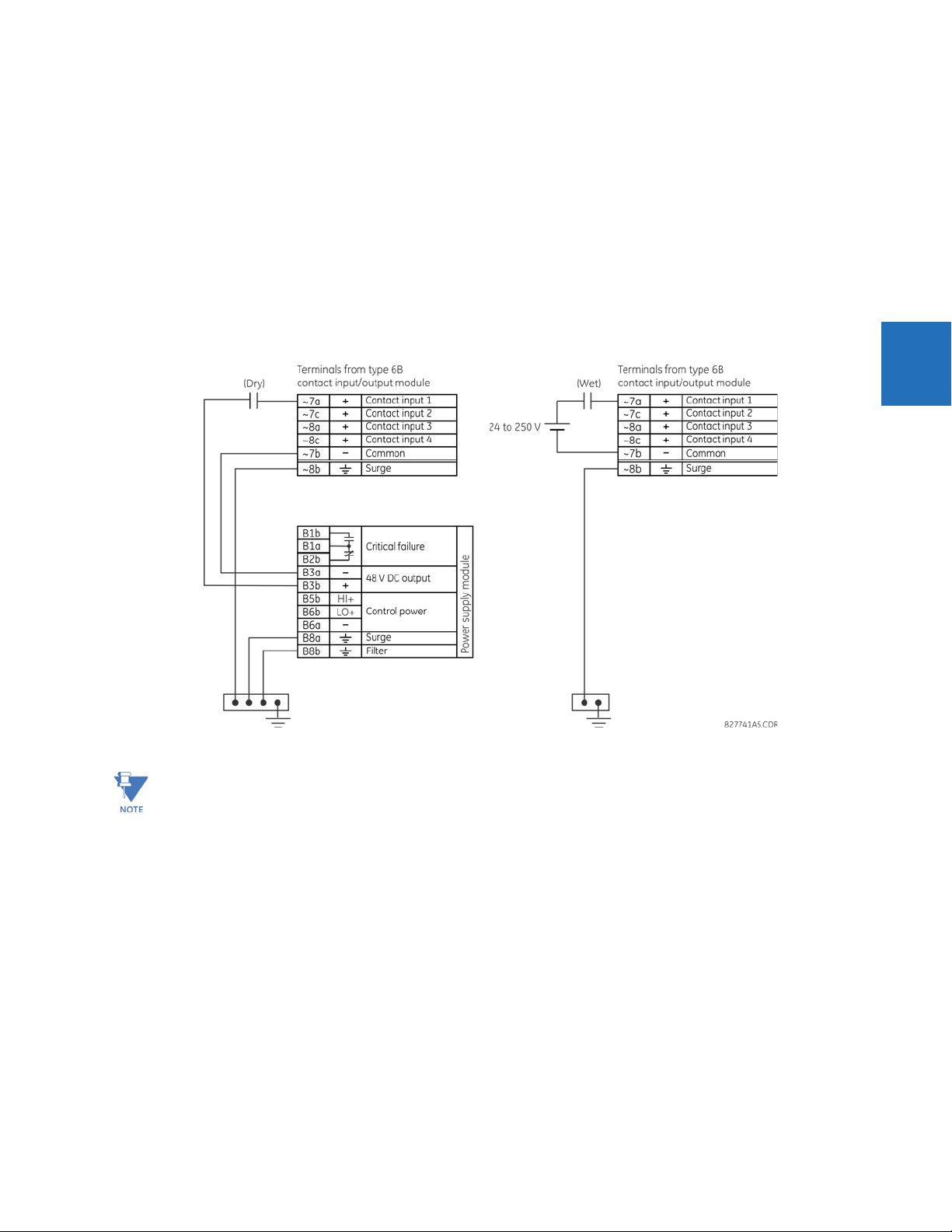
CHAPTER 3: INSTALLATION WIRING
3.3.6.1 Contact inputs
A dry contact has one side connected to terminal B3b. This is the positive 48 V DC voltage rail supplied by the power supply
module. The other side of the dry contact is connected to the required contact input terminal. Each contact input group
has its own common (negative) terminal that must be connected to the DC negative terminal (B3a) of the power supply
module. When a dry contact closes, a current of 1 to 3 mA flows through the associated circuit.
A wet contact has one side connected to the positive terminal of an external DC power supply. The other side of this
contact is connected to the required contact input terminal. If a wet contact is used, then the negative side of the external
source must be connected to the relay common (negative) terminal of each contact group. The maximum external source
voltage for this arrangement is 300 V DC.
The voltage threshold at which each group of four contact inputs detects a closed contact input is programmable as
17 V DC for 24 V sources, 33 V DC for 48 V sources, 84 V DC for 110 to 125 V sources, and 166 V DC for 250 V sources.
Figure 3-16: Dry and wet contact input connections
3
Where a tilde “~” symbol appears, substitute the slot position of the module.
There is no provision in the relay to detect a DC ground fault on 48 V DC control power external output. We recommend
using an external DC supply.
Contacts outputs of protective relays, auxiliary switches from breakers, disconnectors and other devices, are generally
connected to contacts inputs of protective relays. In some situations, the contact outputs of some protective relays can
have high impedance connected across it. When such a contact output is connected across a C70 contact input, it can
spuriously operate the C70 input even when the output is open, if there is a substantial distributed capacitance
(represented by C1) present in the wiring between the output and the C70 input and the debounce time setting in the C70
relay is low enough. This false assertion of the contact input, when there is inadvertent ground present at the DC positive
terminal, can be prevented by inserting a resistor across the C70 input.
The following figure shows a typical DC circuit, with battery ground detection, of contact input . The contact output has
apparent impedance across it (represented by R1).
C70 CAPACITOR BANK PROTECTION AND CONTROL SYSTEM – INSTRUCTION MANUAL 3-21
Page 70

3
WIRING CHAPTER 3: INSTALLATION
Figure 3-17: Typical contact input DC circuit
The presence of the impedance path (R1) across the contact output allows the stray (distributed) capacitance to charge as
shown, thus developing a voltage across the contact input enough to momentarily operate the input while the
capacitance discharges in the presence of DC ground on the positive terminal of the battery.
The duration of the discharge depends on the value of the distributed capacitance, the initial voltage of the distributed
capacitance, and the input impedance of the contact input. If the duration is greater than the debounce time setting, then
the contact input operates.
The application example that follows describes how to mitigate this problem by connecting a resistor across the contact
input, as shown in the next figure, or by adjusting the debounce time setting to a value greater than the discharge time to
prevent spurious operation of the contact input only if the voltage (with output open) across the contact input due to trickle
current is less than the threshold voltage. This operation of contact inputs also can be prevented by using the Auto-Burnish
contact inputs.
Figure 3-18: Contact input connected to a contact output with resistor (R2) across the input
Application example
This example is for illustrative purposes only and the calculations present the worst-case scenario. In practice, the value of
debounce time can be lower.
Contact input ON state impedance used in the calculation of the discharge period is based on the following table.
3-22 C70 CAPACITOR BANK PROTECTION AND CONTROL SYSTEM – INSTRUCTION MANUAL
Page 71

CHAPTER 3: INSTALLATION WIRING
Table 3-4: Discharge period
Battery voltage (V) Input impedance (kΩ)
130 50
250 97
Debounce time setting = 2 ms
Assume a stray capacitance of 0.1 μF.
Assume an initial voltage across the stray capacitance "Vinitial" = 19 V (Vthreshold - 65 V).
Therefore, discharge time constant (τ) =50 kΩ *0.1 μF = 5 ms.
Discharge period t is calculated from the following equation:
Vthreshold = (Vbatt - VInitial) *e^ (-t/τ)
84 = -149 *e^ (t/0.005) Eq. 3-1
T = -0.005 * ln (84/149) = 0.0029 s
Therefore, in this example the contact inputs operate.
To prevent this operation, the debounce time must be increased to 4 ms (set debounce time as per the following table) or
insert a resistor less than or equal to "R" as calculated later.
Table 3-5: Typical debounce time setting
Stray capacitance (μF) Battery voltage (V) Debounce time (ms)
0.05 130 2
0.1 130 4
0.2 130 6
0.05 250 3
0.1 250 6
0.2 250 11
3
The value of this resistor "R" is calculated as follows:
1. Determine the minimum voltage (V threshold) required to turn on the input. This is determined by direct measurement
or referenced in the input specifications.
2. Calculate the resistance necessary to limit the voltage to 1/3 V threshold (when the contact is Open) as follows:
R = (Vthreshold / 3) / (2 mA*) Eq. 3-2
The 2 mA current is used in case the contact input is connected across the GE Form A contact output with voltage
monitoring. Otherwise use the amperage of the active circuit connected to the contact input when its contact output
is open and the voltage across the contact input is third trigger threshold to calculate the resistor value.
3. When the contact is closed, the battery voltage appears across the resistor. The wattage rating of the resistor is then:
PR = 1.3 * (Vbatt) ^2 / R Watts Eq. 3-3
4. Applying the following equation to our example:
R = 84 V / 3*(1 / 2 mA) = 14 kΩ
PR = 1.57 Watts Eq. 3-4
5. Calculating the voltage across the contact input with the Burden Resistor, Voltage across the contact Input:
Vresistor = 2 mA * 14 Kohm = 28 V
Vresistor < contact input threshold (84 V) Eq. 3-5
In conclusion, in this example, the contact input does NOT operate falsely with the Burden Resistor across its input AND
when a battery ground is present.
C70 CAPACITOR BANK PROTECTION AND CONTROL SYSTEM – INSTRUCTION MANUAL 3-23
Page 72

3
WIRING CHAPTER 3: INSTALLATION
3.3.6.2 Use of contact inputs with auto-burnishing
The contact inputs sense a change of the state of the external device contact based on the measured current. When
external devices are located in a harsh industrial environment (either outdoor or indoor), their contacts can be exposed to
various types of contamination. Normally, there is a thin film of insulating sulfidation, oxidation, or contaminates on the
surface of the contacts, sometimes making it difficult or impossible to detect a change of the state. This film must be
removed to establish circuit continuity — an impulse of higher than normal current can accomplish this.
The contact inputs with auto-burnish create a high current impulse when the threshold is reached to burn off this oxidation
layer as a maintenance to the contacts. Afterwards the contact input current is reduced to a steady-state current. The
impulse has a five-second delay after a contact input changes state.
Figure 3-19: Current through contact inputs with auto-burnishing
Regular contact inputs limit current to less than 3 mA to reduce station battery burden. In contrast, contact inputs with
auto-burnishing allow currents up to 50 to 70 mA at the first instance when the change of state was sensed. Then, within
25 to 50 ms, this current is slowly reduced to 3 mA as indicated. The 50 to 70 mA peak current burns any film on the
contacts, allowing for proper sensing of state changes. If the external device contact is bouncing, the auto-burnishing
starts when external device contact bouncing is over.
Another important difference between the auto-burnishing input module and the regular input modules is that only two
contact inputs have common ground, as opposed to four contact inputs sharing one common ground (see the Contact
Input and Output Module Wiring diagrams). This is beneficial when connecting contact inputs to separate voltage sources.
Consequently, the threshold voltage setting is also defined per group of two contact inputs.
The auto-burnish feature can be disabled or enabled using the DIP switches found on each daughter card. There is a DIP
switch for each contact, for a total of 16 inputs.
Figure 3-20: Auto-burnish DIP switches
3-24 C70 CAPACITOR BANK PROTECTION AND CONTROL SYSTEM – INSTRUCTION MANUAL
Page 73

CHAPTER 3: INSTALLATION WIRING
The auto-burnish circuitry has an internal fuse for safety purposes. During regular maintenance, check the auto-burnish
functionality using an oscilloscope.
3.3.6.3 Use of contact inputs with active impedance
In case of external devices that are susceptible to parasitic capacitance of long cable runs affected by switching surges
from external circuits, that can cause inadvertent activation of contact inputs with the external contact open, GE
recommends using the Digital I/O module with active impedance circuit.
Active impedance contact input can tolerate external capacitance of up to 0.2 µF, without entering the ON state for more
than 2 ms. The contact input debounce time can be set above 2 ms to prevent the transient ON state from being internally
used by the relay logic.
The figure shows the active impedance contact input V-I characteristic.
Figure 3-21: Active impedance contact input V-I characteristic
3
A contact input is in LOW state during non-operated system condition, and actively switches to HIGH state upon detection
of input voltage above the settable threshold. The contact input is in the ON (operated state) if the input voltage is to the
right of the threshold band (+/-10% tolerance), and the contact input is in the OFF (non-activated state) when input voltage
is to the left of the band.
C70 CAPACITOR BANK PROTECTION AND CONTROL SYSTEM – INSTRUCTION MANUAL 3-25
Page 74

3
WIRING CHAPTER 3: INSTALLATION
3.3.7 Transducer inputs and outputs
Transducer input modules can receive input signals from external DCmA output transducers (DCmA In) or resistance
temperature detectors (RTDs). Hardware and software are provided to receive signals from these external transducers and
convert these signals into a digital format for use as required.
Transducer output modules provide DC current outputs in several standard DCmA ranges. Software is provided to
configure virtually any analog quantity used in the relay to drive the analog outputs.
Every transducer input/output module has a total of 24 terminal connections. These connections are arranged as three
terminals per row with a total of eight rows. A given row can be used for either inputs or outputs, with terminals in column
"a" having positive polarity and terminals in column "c" having negative polarity. Since an entire row is used for a single
input/output channel, the name of the channel is assigned using the module slot position and row number.
Each module also requires that a connection from an external ground bus be made to terminal 8b. The current outputs
require a twisted-pair shielded cable, where the shield is grounded at one end only. The following figure illustrates the
transducer module types (5A, 5C, 5D, 5E, and 5F) and channel arrangements that can be ordered for the relay.
Where a tilde “~” symbol appears, substitute the slot position of the module.
Figure 3-22: Transducer input/output module wiring
The following figure show how to connect RTDs.
3-26 C70 CAPACITOR BANK PROTECTION AND CONTROL SYSTEM – INSTRUCTION MANUAL
Page 75

CHAPTER 3: INSTALLATION WIRING
Figure 3-23: RTD connections
3
3.3.8 RS232 faceplate port
A nine-pin RS232C serial port is located on the faceplate for programming with a computer. All that is required to use this
interface is a computer running the EnerVista UR Setup software provided with the relay. Cabling for the RS232 port is
shown in the following figure for both 9-pin and 25-pin connectors.
The baud rate for this port can be set, with a default of 115200 bps.
C70 CAPACITOR BANK PROTECTION AND CONTROL SYSTEM – INSTRUCTION MANUAL 3-27
Page 76

3
WIRING CHAPTER 3: INSTALLATION
Figure 3-24: RS232 faceplate port connection
3.3.9 CPU communication ports
3.3.9.1 Overview
In addition to the faceplate RS232 port , there is a rear RS485 communication port.
The CPU modules do not require a surge ground connection.
3-28 C70 CAPACITOR BANK PROTECTION AND CONTROL SYSTEM – INSTRUCTION MANUAL
Page 77

CHAPTER 3: INSTALLATION WIRING
Figure 3-25: CPU module communications wiring
3
3.3.9.2 RS485 port
RS485 data transmission and reception are accomplished over a single twisted-pair wire with transmit and receive data
alternating over the same two wires. Through the use of the port, continuous monitoring and control from a remote
computer, SCADA system, or Power Line Carrier (PLC) is possible.
To minimize errors from noise, the use of shielded twisted-pair wire is recommended. Correct polarity must be observed.
For instance, the relays must be connected with all RS485 “+” terminals connected together, and all RS485 “–” terminals
connected together. Though data is transmitted over a two-wire twisted pair, all RS485 devices require a shared reference,
or common voltage. This common voltage is implied to be a power supply common. Some systems allow the shield (drain
wire) to be used as common wire and to connect directly to the C70 COM terminal (#3); others function correctly only if the
common wire is connected to the C70 COM terminal, but insulated from the shield.
To avoid loop currents, ground the shield at only one point. If other system considerations require the shield to be
grounded at more than one point, install resistors (typically 100 ohms) between the shield and ground at each grounding
point. Each relay needs to be daisy-chained to the next one in the link. A maximum of 32 relays can be connected in this
manner without exceeding driver capability. For larger systems, additional serial channels must be added. It is also
possible to use commercially available repeaters to have more than 32 relays on a single channel. Avoid star or stub
connections entirely.
C70 CAPACITOR BANK PROTECTION AND CONTROL SYSTEM – INSTRUCTION MANUAL 3-29
Page 78

3
WIRING CHAPTER 3: INSTALLATION
Lightning strikes and ground surge currents can cause large momentary voltage differences between remote ends of the
communication link. For this reason, surge protection devices are provided internally at both communication ports. An
isolated power supply with an optocoupled data interface also acts to reduce noise coupling. To ensure maximum
reliability, ensure that all equipment has similar transient protection devices installed.
Terminate both ends of the RS485 circuit with an impedance as shown in the figure.
Figure 3-26: RS485 serial connection
3.3.9.3 100Base-FX fiber optic ports
The fiber optic communication ports allow for fast and efficient communications between relays at 100 Mbps. Optical fiber
can be connected to the relay supporting a wavelength of 1310 nm in multimode.
Ensure that the dust covers are installed when the fiber is not in use. Dirty or scratched connectors can lead to high losses
on a fiber link.
3.3.10 IRIG-B
IRIG-B is a standard time code format that allows stamping of events to be synchronized among connected devices. The
IRIG-B code allows time accuracies of up to 100 ns. Using the IRIG-B input, the C70 operates an internal oscillator with 1 µs
resolution and accuracy. The IRIG time code formats are serial, pulse width-modulated codes that can be either DC level
shifted or amplitude modulated (AM). The GE MultiSync 100 1588 GPS Clock as well as third-party equipment are available
for generating the IRIG-B signal; this equipment can use a global positioning system (GPS) satellite system to obtain the
time reference so that devices at different geographic locations can be synchronized.
3-30 C70 CAPACITOR BANK PROTECTION AND CONTROL SYSTEM – INSTRUCTION MANUAL
Page 79

CHAPTER 3: INSTALLATION DIRECT INPUT AND OUTPUT COMMUNICATIONS
Figure 3-27: Options for the IRIG-B connection
3
Using an amplitude-modulated receiver causes errors up to 1 ms in event time stamping.
3.4 Direct input and output communications
3.4.1 Description
The direct inputs and outputs feature makes use of the type 7 series of communications modules and allows direct
messaging between UR devices. The communications modules are outlined in the table later in this section.
The communications channels are normally connected in a ring configuration, as shown in the following figure. The
transmitter of one module is connected to the receiver of the next module. The transmitter of this second module is then
connected to the receiver of the next module in the ring. This is continued to form a communications ring. The figure
illustrates a ring of four UR-series relays with the following connections: UR1-Tx to UR2-Rx, UR2-Tx to UR3-Rx, UR3-Tx to
UR4-Rx, and UR4-Tx to UR1-Rx. A maximum of 16 URs can be connected in a single ring.
C70 CAPACITOR BANK PROTECTION AND CONTROL SYSTEM – INSTRUCTION MANUAL 3-31
Page 80

3
DIRECT INPUT AND OUTPUT COMMUNICATIONS CHAPTER 3: INSTALLATION
Figure 3-28: Direct input and output single-channel connection
IRC modules with protocol C37.94 and G.703 are designed for back-to-back communication connections, so the ring
configuration shown in the previous figure does not apply. To establish inter-relay communication in more than two URs,
you need to have two channel IRC module and enable DIRECT I/O CHANNEL CROSSOVER function in all relays, as shown in
the next figure. This configuration can be expanded to 16 URs, and this configuration does not provide redundancy ring
since both channels are made into single ring by the channel crossover function. As per the figure Typical Pin
Interconnection between Two G.703 Interfaces later in this chapter, the clock is supplied typically by multiplexer (MUX) and
all URs are in Loop Timing Mode. If there is no MUX, then UR1 and UR3 can be in Internal Timing Mode and UR2 and UR4
can be in Loop Timing Mode. That is, connected channels must have opposite timing modes.
Figure 3-29: Ring configuration for C37.94 module (concept also applies to G.703)
The interconnection for dual-channel type 7 communications modules is shown as follows. Two-channel modules allow for
a redundant ring configuration. That is, two rings can be created to provide an additional independent data path. The
required connections are: UR1-Tx1 to UR2-Rx1, UR2-Tx1 to UR3-Rx1, UR3-Tx1 to UR4-Rx1, and UR4-Tx1 to UR1-Rx1 for the
first ring; and UR1-Tx2 to UR4-Rx2, UR4-Tx2 to UR3-Rx2, UR3-Tx2 to UR2-Rx2, and UR2-Tx2 to UR1-Rx2 for the second ring.
3-32 C70 CAPACITOR BANK PROTECTION AND CONTROL SYSTEM – INSTRUCTION MANUAL
Page 81

CHAPTER 3: INSTALLATION DIRECT INPUT AND OUTPUT COMMUNICATIONS
Figure 3-30: Direct input and output dual-channel connection
3
The following diagram shows the connection for three UR-series relays using two independent communication channels.
UR1 and UR3 have single type 7 communication modules; UR2 has a dual-channel module. The two communication
channels can be of different types, depending on the type 7 modules used. To allow the direct input and output data to
cross-over from channel 1 to channel 2 on UR2, set the
forces UR2 to forward messages received on Rx1 out Tx2, and messages received on Rx2 out Tx1.
Figure 3-31: Direct input and output single/dual channel combination connection
The inter-relay communications modules are available with several interfaces and some are outlined here in more detail.
Those that apply depend on options purchased. The options are outlined in the Inter-Relay Communications section of the
Order Code tables in Chapter 2. All of the fiber modules use ST type connectors.
DIRECT I/O CHANNEL CROSSOVER setting to “Enabled” on UR2. This
C70 CAPACITOR BANK PROTECTION AND CONTROL SYSTEM – INSTRUCTION MANUAL 3-33
Page 82

3
DIRECT INPUT AND OUTPUT COMMUNICATIONS CHAPTER 3: INSTALLATION
3.4.2 Fiber: LED and ELED transmitters
The following figure shows the configuration for the 7A, 7B, 7C, 7H, 7I, and 7J fiber-only modules.
Figure 3-32: LED and ELED fiber modules
3.4.3 G.703 interface
3.4.3.1 Description
The following figure shows the 64K ITU G.703 co-directional interface configuration.
The G.703 module is fixed at 64 kbps. The
applicable to this module.
AWG 24 twisted shielded pair is recommended for external connections, with the shield grounded only at one end.
Connecting the shield to pin X1a or X6a grounds the shield since these pins are connected internally to ground. Thus, if
pin X1a or X6a is used to ground the shield at one end, do not ground the shield at the other end. This interface module is
protected by surge suppression devices.
SETTINGS PRODUCT SETUP DIRECT I/O DIRECT I/O DATA RATE setting is not
Figure 3-33: G.703 interface configuration
The following figure shows the typical pin interconnection between two G.703 interfaces. For the actual physical
arrangement of these pins, see the Rear Terminal Layout section earlier in this chapter. All pin interconnections are to be
maintained for a connection to a multiplexer.
3-34 C70 CAPACITOR BANK PROTECTION AND CONTROL SYSTEM – INSTRUCTION MANUAL
Page 83

CHAPTER 3: INSTALLATION DIRECT INPUT AND OUTPUT COMMUNICATIONS
Figure 3-34: Typical pin interconnection between two G.703 interfaces
Pin nomenclature differs from one manufacturer to another. It is not uncommon to see pinouts numbered TxA, TxB,
RxA, and RxB. In such cases, assume that “A” is equivalent to “+” and “B” is equivalent to “–.”
3.4.3.2 G.703 selection switch procedures
1. With the power to the relay off, remove the G.703 module (7R or 7S) as follows. Record the original location of the
module to help ensure that the same or replacement module is inserted into the correct slot.
2. Simultaneously pull the ejector/inserter clips located at the top and at the bottom of each module in order to release
the module for removal. (For more information on accessing modules, see the Maintenance chapter.)
3. Remove the module cover screw.
4. Remove the top cover by sliding it towards the rear and then lift it upwards.
5. Set the timing selection switches (channels 1 and 2) to the required timing modes.
6. Replace the top cover and the cover screw.
7. Re-insert the G.703 module. Take care to ensure that the correct module type is inserted into the correct slot position.
The ejector/inserter clips located at the top and bottom of each module must be in the disengaged position as the
module is inserted smoothly into the slot. Once the clips have cleared the raised edge of the chassis, engage the clips
simultaneously. When the clips have locked into position, the module is inserted fully.
3
C70 CAPACITOR BANK PROTECTION AND CONTROL SYSTEM – INSTRUCTION MANUAL 3-35
Page 84

3
DIRECT INPUT AND OUTPUT COMMUNICATIONS CHAPTER 3: INSTALLATION
Figure 3-35: G.703 timing selection switch setting
Table 3-6: G.703 timing selections
Switches Function
S1 OFF → octet timing disabled
S5 and S6 S5 = OFF and S6 = OFF → loop timing mode
ON → octet timing 8 kHz
S5 = ON and S6 = OFF → internal timing mode
S5 = OFF and S6 = ON → minimum remote loopback mode
S5 = ON and S6 = ON → dual loopback mode
3.4.3.3 G.703 octet timing
If octet timing is enabled (ON), this 8 kHz signal is asserted during the violation of bit 8 (LSB) necessary for connecting to
higher order systems. When C70s are connected back-to-back, octet timing is disabled (OFF).
3.4.3.4 G.703 timing modes
There are two timing modes for the G.703 module: internal timing mode and loop timing mode (default).
• Internal Timing Mode — The system clock is generated internally. Therefore, set the G.703 timing selection to internal
timing mode for back-to-back (UR-to-UR) connections. For back-to-back connections, set octet timing (S1 = OFF) and
timing mode to internal timing (S5 = ON and S6 = OFF).
• Loop Timing Mode — The system clock is derived from the received line signal. Therefore, set the G.703 timing
selection to loop timing mode for connections to higher order systems. For connection to a higher order system (URto-multiplexer, factory defaults), set to octet timing (S1 = ON) and set timing mode to loop timing (S5 = OFF and S6 =
OFF).
The switch settings for the internal and loop timing modes are shown.
3-36 C70 CAPACITOR BANK PROTECTION AND CONTROL SYSTEM – INSTRUCTION MANUAL
Page 85

CHAPTER 3: INSTALLATION DIRECT INPUT AND OUTPUT COMMUNICATIONS
Figure 3-36: Switches
3.4.3.5 G.703 test modes
In minimum remote loopback mode, the multiplexer is enabled to return the data from the external interface without any
processing to assist in diagnosing G.703 line-side problems irrespective of clock rate. Data enters from the G.703 inputs,
passes through the data stabilization latch that also restores the proper signal polarity, passes through the multiplexer and
then returns to the transmitter. The differential received data is processed and passed to the G.703 transmitter module
after which point the data is discarded. The G.703 receiver module is fully functional and continues to process data and
passes it to the differential Manchester transmitter module. Since timing is returned as it is received, the timing source is
expected to be from the G.703 line side of the interface.
Figure 3-37: G.703 minimum remote loopback mode
3
In dual loopback mode, the multiplexers are active and the functions of the circuit are divided into two with each receiver/
transmitter pair linked together to deconstruct and then reconstruct their respective signals. Differential Manchester data
enters the Differential Manchester receiver module and then is returned to the differential Manchester transmitter module.
Likewise, G.703 data enters the G.703 receiver module and is passed through to the G.703 transmitter module to be
returned as G.703 data. Because of the complete split in the communications path and because, in each case, the clocks
are extracted and reconstructed with the outgoing data, in this mode there must be two independent sources of timing.
One source lies on the G.703 line side of the interface while the other lies on the differential Manchester side of the
interface.
Figure 3-38: G.703 dual loopback mode
C70 CAPACITOR BANK PROTECTION AND CONTROL SYSTEM – INSTRUCTION MANUAL 3-37
Page 86

3
DIRECT INPUT AND OUTPUT COMMUNICATIONS CHAPTER 3: INSTALLATION
3.4.4 RS422 interface
3.4.4.1 Description
There are two RS422 inter-relay communications modules available: single-channel RS422 (module 7T) and dual-channel
RS422 (module 7W). The modules can be configured to run at 64 kbps or 128 kbps. AWG 20-24 twisted shielded pair cable
is recommended for external connections. These modules are protected by optically-isolated surge suppression devices.
The shield pins (6a and 7b) are connected internally to the ground pin (8a). Proper shield termination is as follows:
• Site 1 — Terminate shield to pins 6a or 7b or both
• Site 2 — Terminate shield to COM pin 2b
Match the clock terminating impedance with the impedance of the line.
Figure 3-39: RS422 interface connections
The following figure shows the typical pin interconnection between two single-channel RS422 interfaces installed in slot W.
All pin interconnections are to be maintained for a connection to a multiplexer.
Figure 3-40: Typical pin interconnect between two RS422 interfaces
3.4.4.2 Two-channel application via multiplexers
The RS422 interface can be used for single-channel or two-channel applications over SONET/SDH or multiplexed systems.
When used in single-channel applications, the RS422 interface links to higher-order systems in a typical way, observing
transmit (Tx), receive (Rx), and send timing (ST) connections. However, when used in two-channel applications, certain
criteria must be followed since there is one clock input for the two RS422 channels. The system functions correctly when
the following connections are observed and your data module has a terminal timing feature. Terminal timing is a common
feature to most synchronous data units that allows the module to accept timing from an external source. Using the
terminal timing feature, two-channel applications can be achieved if these connections are followed: the send timing
outputs from the multiplexer (data module 1) connects to the clock inputs of the UR RS422 interface in the usual way. In
3-38 C70 CAPACITOR BANK PROTECTION AND CONTROL SYSTEM – INSTRUCTION MANUAL
Page 87

CHAPTER 3: INSTALLATION DIRECT INPUT AND OUTPUT COMMUNICATIONS
addition, the send timing outputs of data module 1 are also paralleled to the terminal timing inputs of data module 2. By
using this configuration, the timing for both data modules and both UR RS422 channels are derived from a single clock
source. As a result, data sampling for both of the UR RS422 channels is synchronized via the send timing leads on data
module 1, shown as follows. If the terminal timing feature is not available or this type of connection is not wanted, the
G.703 interface is a viable option that does not impose timing restrictions.
Figure 3-41: Timing configuration for RS422 two-channel, three-terminal application
3
Data module 1 provides timing to the C70 RS422 interface via the ST(A) and ST(B) outputs. Data module 1 also provides
timing to data module 2 TT(A) and TT(B) inputs via the ST(A) and AT(B) outputs. The data module pin numbers have been
omitted in the figure because they vary by manufacturer.
3.4.4.3 Transmit timing
The RS422 interface accepts one clock input for transmit timing. It is important that the rising edge of the 64 kHz transmit
timing clock of the multiplexer interface is sampling the data in the center of the transmit data window. Therefore, it is
important to confirm clock and data transitions to ensure proper system operation. For example, the following figure
shows the positive edge of the Tx clock in the center of the Tx data bit.
C70 CAPACITOR BANK PROTECTION AND CONTROL SYSTEM – INSTRUCTION MANUAL 3-39
Page 88

3
DIRECT INPUT AND OUTPUT COMMUNICATIONS CHAPTER 3: INSTALLATION
Figure 3-42: Clock and data transitions
3.4.4.4 Receive timing
The RS422 interface utilizes NRZI-MARK modulation code and therefore does not rely on an Rx clock to recapture data.
NRZI-MARK is an edge-type, invertible, self-clocking code.
To recover the Rx clock from the data-stream, an integrated digital phase lock loop (DPLL) circuit is utilized. The DPLL is
driven by an internal clock, which is 16-times over-sampled, and uses this clock along with the data-stream to generate a
data clock that can be used as the serial communication controller (SCC) receive clock.
3.4.5 IEEE C37.94 interface
The UR-series IEEE C37.94 communication modules (module types 2I, 2J, 76, and 77) are designed to interface with IEEE
C37.94 compliant digital multiplexers or an IEEE C37.94 compliant interface converter for use with direct input and output
applications. The IEEE C37.94 standard defines a point-to-point optical link for synchronous data between a multiplexer
and a teleprotection device. This data is typically 64 kbps, but the standard provides for speeds up to 64n kbps, where n =
1, 2,…, 12. The UR-series C37.94 communication modules are either 64 kbps (with n fixed at 1) for 128 kbps (with n fixed at
2). The frame is a valid International Telecommunications Union (ITU-T) recommended G.704 pattern from the standpoint
of framing and data rate. The frame is 256 bits and is repeated at a frame rate of 8000 Hz, with a resultant bit rate of 2048
kbps.
The specifications for the module are as follows:
• IEEE standard — C37.94 for 2 × 64 kbps optical fiber interface (for 76 and 77 modules)
• Fiber optic cable type — 50 nm or 62.5 μm core diameter optical fiber
• Fiber optic mode — multimode
• Fiber optic cable length — up to 2 km
• Fiber optic connector — type ST
• Wavelength — 820 ±40 nm
• Connection — as per all fiber optic connections, a Tx to Rx connection is required
The UR-series C37.94 communication module can be connected directly to any compliant digital multiplexer that supports
the IEEE C37.94 standard. The figure shows the concept.
3-40 C70 CAPACITOR BANK PROTECTION AND CONTROL SYSTEM – INSTRUCTION MANUAL
Page 89

CHAPTER 3: INSTALLATION DIRECT INPUT AND OUTPUT COMMUNICATIONS
Figure 3-43: IEEE C37.94 connection to compliant digital multiplexer
The UR-series C37.94 communication module can be connected to the electrical interface (G.703, RS422, or X.21) of a noncompliant digital multiplexer via an optical-to-electrical interface converter that supports the IEEE C37.94 standard. The
following figure shows the concept.
Figure 3-44: IEEE C37.94 connection to non-compliant digital multiplexer
In 2008, GE Grid Solutions released revised modules 76 and 77 for C37.94 communication to enable multi-ended fault
location functionality with firmware 5.60 release and higher. All modules 76 and 77 shipped since the change support this
feature and are fully backward compatible with firmware releases below 5.60. For customers using firmware release 5.60
and higher, the module can be identified with "Rev D" printed on the module and is to be used on all ends of C70
communication for two and three terminal applications. Failure to use it at all ends results in intermittent communication
alarms. For customers using firmware revisions below 5.60, it is not required to match the revision of the modules installed.
The UR-series C37.94 communication module has six switches to set the clock configuration. The following figure shows
the functions of these control switches.
Figure 3-45: Switches
3
For the internal timing mode, the system clock is generated internally. Therefore, set the timing switch selection to internal
timing for relay 1 and loop timed for relay 2. There must be only one timing source configured.
For the looped timing mode, the system clock is derived from the received line signal. Therefore, set the timing selection to
loop timing mode for connections to higher order systems.
The IEEE C37.94 communications module cover removal procedure is as follows:
1. With power to the relay off, remove the IEEE C37.94 module (type 2I, 2J, 76, or 77 module) as follows. Record the
original location of the module to help ensure that the same or replacement module is inserted into the correct slot.
2. Simultaneously pull the ejector/inserter clips located at the top and bottom of each module in order to release the
module for removal.
3. Remove the module cover screw.
4. Remove the top cover by sliding it towards the rear and then lift it upwards.
C70 CAPACITOR BANK PROTECTION AND CONTROL SYSTEM – INSTRUCTION MANUAL 3-41
Page 90

3
DIRECT INPUT AND OUTPUT COMMUNICATIONS CHAPTER 3: INSTALLATION
5. Set the timing selection switches (channels 1 and 2) to the required timing modes (see description earlier).
6. Replace the top cover and the cover screw.
7. Re-insert the IEEE C37.94 module. Take care to ensure that the correct module type is inserted into the correct slot
position. The ejector/inserter clips located at the top and at the bottom of each module must be in the disengaged
position as the module is inserted smoothly into the slot. Once the clips have cleared the raised edge of the chassis,
engage the clips simultaneously. When the clips have locked into position, the module is inserted fully.
Figure 3-46: IEEE C37.94 timing selection switch setting
Modules shipped since January 2012 have status LEDs that indicate the status of the DIP switches, as shown in the
following figure.
3-42 C70 CAPACITOR BANK PROTECTION AND CONTROL SYSTEM – INSTRUCTION MANUAL
Page 91

CHAPTER 3: INSTALLATION ACTIVATE RELAY
Figure 3-47: Status LEDs
3
The clock configuration LED status is as follows:
• Flashing green — loop timing mode while receiving a valid data packet
• Flashing yellow — internal mode while receiving a valid data packet
• Solid red — (switch to) internal timing mode while not receiving a valid data packet
The link/activity LED status is as follows:
• Flashing green — FPGA is receiving a valid data packet
• Solid yellow — FPGA is receiving a "yellow bit" and remains yellow for each "yellow bit"
• Solid red — FPGA is not receiving a valid packet or the packet received is invalid
3.5 Activate relay
The relay is in the default “Not Programmed” state when it leaves the factory. When powered up successfully, the "Trouble"
LED is on and the "In Service" LED is off. The relay in the “Not Programmed” state blocks signaling of any output relay. These
conditions remain until the relay is explicitly put in the “Programmed” state.
RELAY SETTINGS:
Not Programmed
The relay can be activated on the front panel or in the EnerVista software.
To activate the relay using the front panel:
1. Press the
2. Press the
3. Press the
4. Press the
MENU key until the SETTINGS header flashes momentarily and the PRODUCT SETUP message displays.
MESSAGE right arrow until the SECURITY message displays.
MESSAGE down arrow until the INSTALLATION message displays.
MESSAGE right arrow until the RELAY SETTINGS: Not Programmed message displays.
When the relay is powered up, the "Trouble LED" is on, the "In Service" LED is off, and this message
displays, indicating that the relay is in the "Not Programmed" state and is safeguarding (output
relays blocked) against the installation of a relay whose settings have not been entered. This
message remains until the relay is explicitly put in the "Programmed" state.
C70 CAPACITOR BANK PROTECTION AND CONTROL SYSTEM – INSTRUCTION MANUAL 3-43
Page 92

INSTALL SOFTWARE CHAPTER 3: INSTALLATION
SETTINGS
SETTINGS
PRODUCT SETUP
SECURITY
DISPLAY
PROPERTIES
3
INSTALLATION
5. After the RELAY SETTINGS: Not Programmed message displays, press a VALUE key to change the selection to
"Programmed."
6. Press the
RELAY SETTINGS:
Not Programmed
7. When the "NEW SETTING HAS BEEN STORED" message appears, the relay is in "Programmed" state and the "In Service"
LED turns on.
To activate the relay using EnerVista software:
1. Navigate to Settings > Product Setup > Installation and change the Relay Settings field to "Programmed."
2. Save the change.
ENTER key to save the change.
RELAY SETTINGS:
Programmed
RELAY SETTINGS:
Not Programmed
NEW SETTING
HAS BEEN STORED
3.6 Install software
3.6.1 EnerVista communication overview
The EnerVista UR Setup software communicates to the relay via the faceplate RS232 port or the rear panel RS485 /
Ethernet ports.
To communicate via the faceplate RS232 port, use a standard straight-through serial cable. Connect the DB-9 male end to
the relay and the DB-9 or DB-25 female end to the computer COM2 port as described in the CPU Communication Ports
section earlier in this chapter.
3-44 C70 CAPACITOR BANK PROTECTION AND CONTROL SYSTEM – INSTRUCTION MANUAL
Page 93

CHAPTER 3: INSTALLATION INSTALL SOFTWARE
Figure 3-48: Relay communication options
3
To communicate through the C70 rear RS485 port from a computer RS232 port, the GE Grid Solutions RS232/RS485
converter box is required. This device (catalog number F485) connects to the computer using a straight-through serial
cable. A shielded twisted-pair (20, 22, or 24 AWG) connects the F485 converter to the C70 rear communications port. The
converter terminals (+, –, GND) are connected to the C70 communication module (+, –, COM) terminals. See the CPU
Communication Ports section in chapter 3 for details. The line is terminated with an R-C network (that is, 120 Ω, 1 nF) as
described in this chapter.
3.6.2 System requirements
The relay front panel or the EnerVista UR Setup software can be used to communicate with the relay. The software
interface is the preferred method to edit settings and view actual values because the computer monitor can display more
information.
The minimum system requirements for the EnerVista software are as follows:
• Intel Pentium processor (dual core)
• Microsoft Windows 7 with Service Pack 1 (32-bit or 64-bit) or Windows Server 2008 Release 2 with Service Pack 1 (64-
bit)
• 1 GB free hard drive space
•2 GB RAM
• 1280 x 800 display screen
C70 CAPACITOR BANK PROTECTION AND CONTROL SYSTEM – INSTRUCTION MANUAL 3-45
Page 94

3
INSTALL SOFTWARE CHAPTER 3: INSTALLATION
3.6.3 Install software
After ensuring that the requirements for using EnerVista UR Setup software are met, there are three ways to install the
software:
•From the DVD
• Download EnerVista Launchpad software from http://www.gegridsolutions.com/multilin
• Download the EnerVista UR Setup software from http://www.gegridsolutions.com/multilin
To install the software from the DVD and using EnerVista Launchpad:
1. Insert the DVD into the DVD drive of your computer.
2. Click the Install Now button and follow the instructions.
3. When installation is complete, start the EnerVista Launchpad application.
4. Click the IED Setup section of the Launch Pad window.
Figure 3-49: Adding a UR device in Launchpad window
and install it
and install it
5. In the EnerVista Launch Pad window, click the Add Product button and select the appropriate product as follows.
Select the Web option to ensure the most recent software release, or select CD if you do not have an Internet
connection, then click the Add Now button to list software items for the product. EnerVista Launchpad obtains the
software from the Internet or DVD and automatically starts the installation program.
Figure 3-50: Identifying the UR device type
6. Select the complete path, including the new directory name, where the EnerVista UR Setup software is to be installed.
7. Click the Next button to begin the installation. The files are installed in the directory indicated, and the installation
program automatically creates icons and adds an entry to the Windows start menu.
3-46 C70 CAPACITOR BANK PROTECTION AND CONTROL SYSTEM – INSTRUCTION MANUAL
Page 95

CHAPTER 3: INSTALLATION ADD DEVICE TO SOFTWARE
8. Click Finish to complete the installation. The UR device is added to the list of installed intelligent electronic devices
(IEDs) in the EnerVista Launchpad window, as shown.
Figure 3-51: UR device added to Launchpad window
3.7 Add device to software
You connect remotely to the C70 through the rear RS485 or Ethernet port with a computer running the EnerVista UR Setup
software. The C70 also can be accessed locally with a computer through the front panel RS232 port or the rear Ethernet
port using the Quick Connect feature.
The following procedures are outlined:
• Add device for serial access; see the Configure Serial Connection section
• Add device for the rear Ethernet port; see the Configure Ethernet Connection section
• Add device for access using a modem; see the Configure Modem Connection section
• Connect locally with a computer through either the front RS232 port or rear Ethernet port; see the Connect to the C70
section
• Discover automatically UR devices within a network; see the Automatic Discovery of UR Devices section
Devices are listed in the order entered in the Device Setup window.
Devices are listed alphabetically in the main software window, for example B30, B90, T35. Use the Device Name to order
them as required, for example B30 Odessa, B30 Truro, B90, T35.
You cannot import a file to add a device to the software. You can import settings as outlined at the end of the chapter.
The Quick Connect button can also be used to add devices. The device is added to a Quick Connect menu item in the
Online Window area, cannot be moved from it to another grouping, and needs to be renamed in the Device Setup window.
GE instead recommends using the Device Setup window to add devices, as outlined here.
3
3.7.1 Set IP address in UR
The IP and subnet addresses need to be added to the UR for Ethernet communication.
For serial communication, for example using the front RS232 port and the Quick Connect feature, the addresses are not
required, but typically they are entered to add/configure devices for regular use.
1. On the front of the C70, press the
2. Navigate to
3. Enter an IP address, for example “1.1.1.1,” and press the
4. In the same menu, select the
5. Enter a subnet IP address, for example “255.0.0.0,” and press the
C70 CAPACITOR BANK PROTECTION AND CONTROL SYSTEM – INSTRUCTION MANUAL 3-47
Settings Product Setup Communications Network IP Address Setting.
MENU key until the Settings menu displays.
ENTER key to save the value.
Subnet IP Mask setting.
ENTER key to save the value.
Page 96
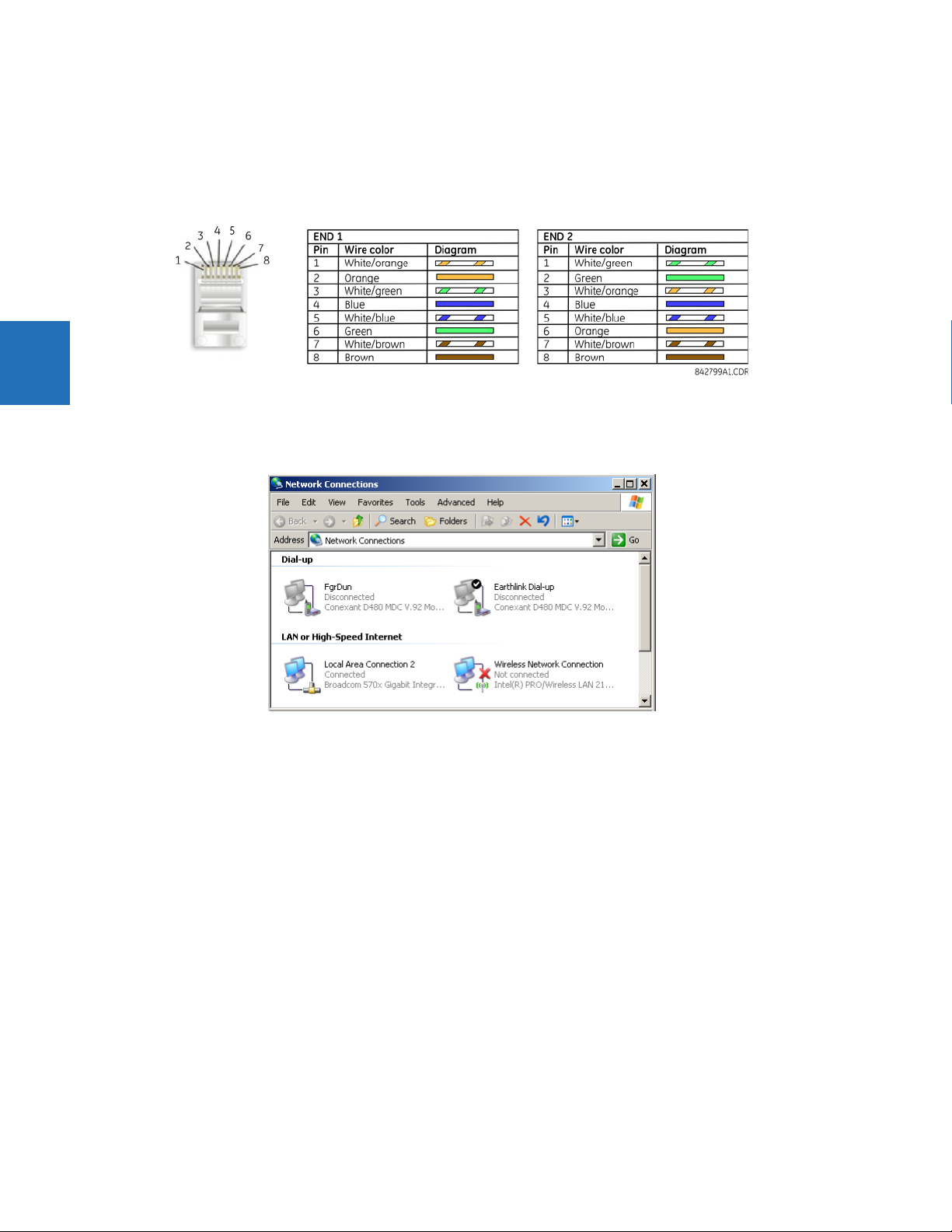
3
ADD DEVICE TO SOFTWARE CHAPTER 3: INSTALLATION
If using a blue or grey Ethernet cable, skip the rest of the this section. If using an orange cross-over Ethernet cable, the
computer needs to be set up as follows.
1. Use an orange Ethernet cross-over cable to connect the computer to the rear Ethernet port. In case you need it, the
following figure shows the pinout for an Ethernet cross-over cable.
Figure 3-52: Ethernet cross-over cable PIN layout
Next, assign the computer an IP address compatible with the relay’s IP address.
1. From the Windows desktop, right-click the My Network Places icon and select Properties to open the network
connections window. Or in Windows 7, access the Network and Sharing Center in the Control Panel.
3-48 C70 CAPACITOR BANK PROTECTION AND CONTROL SYSTEM – INSTRUCTION MANUAL
Page 97

CHAPTER 3: INSTALLATION ADD DEVICE TO SOFTWARE
2. Right-click the Local Area Connection icon and select Properties.
3
3. Select the Internet Protocol (TCP/IP) item from the list, and click the Properties button.
4. Click the “Use the following IP address” box.
5. Enter an IP address with the first three numbers the same as the IP address of the C70 relay and the last number
different (in this example, 1.1.1.2).
6. Enter a subnet mask equal to the one set in the C70 (in this example, 255.0.0.0).
7. Click the OK button to save the values.
C70 CAPACITOR BANK PROTECTION AND CONTROL SYSTEM – INSTRUCTION MANUAL 3-49
Page 98

3
ADD DEVICE TO SOFTWARE CHAPTER 3: INSTALLATION
Before continuing, test the Ethernet connection.
1. Open a Windows console window, for example by selecting Start > Run from the Windows Start menu and typing
“cmd” or clicking the Start button and entering "cmd".
2. Type the following command, substituting the IP address of 1.1.1.1 with yours:
C:\WINNT>ping 1.1.1.1
3. If the connection is successful, the system returns four replies similar to the following:
Pinging 1.1.1.1 with 32 bytes of data:
Reply from 1.1.1.1: bytes=32 time<10ms TTL=255
Reply from 1.1.1.1: bytes=32 time<10ms TTL=255
Reply from 1.1.1.1: bytes=32 time<10ms TTL=255
Reply from 1.1.1.1: bytes=32 time<10ms TTL=255
Ping statistics for 1.1.1.1:
Packets: Sent = 4, Received = 4, Lost = 0 (0% loss),
Approximate round trip time in milliseconds:
Minimum = 0ms, Maximum = 0ms, Average = 0 ms
4. Note that the values for time and TTL vary depending on local network configuration.
5. If the following sequence of messages appears when entering the
Pinging 1.1.1.1 with 32 bytes of data:
Request timed out.
Request timed out.
Request timed out.
Request timed out.
Ping statistics for 1.1.1.1:
Packets: Sent = 4, Received = 0, Lost = 4 (100% loss),
Approximate round trip time in milliseconds:
Minimum = 0ms, Maximum = 0ms, Average = 0 ms
Pinging 1.1.1.1 with 32 bytes of data:
C:\WINNT>ping 1.1.1.1 command:
verify the physical connection between the C70 and the computer, and double-check the programmed IP address in
Product Setup Communications Network IP Address setting, then repeat step 2.
the
6. If the following sequence of messages appears when entering the
Pinging 1.1.1.1 with 32 bytes of data:
Hardware error.
Hardware error.
Hardware error.
Hardware error.
Ping statistics for 1.1.1.1:
Packets: Sent = 4, Received = 0, Lost = 4 (100% loss),
Approximate round trip time in milliseconds:
Minimum = 0ms, Maximum = 0ms, Average = 0 ms
Pinging 1.1.1.1 with 32 bytes of data:
C:\WINNT>ping 1.1.1.1 command:
verify the physical connection between the C70 and the computer, and double-check the programmed IP address in
PRODUCT SETUP COMMUNICATIONS NETWORK IP ADDRESS setting, then repeat step 2.
the
7. If the following sequence of messages appears when entering the
Pinging 1.1.1.1 with 32 bytes of data:
Destination host unreachable.
Destination host unreachable.
Destination host unreachable.
Destination host unreachable.
Ping statistics for 1.1.1.1:
Packets: Sent = 4, Received = 0, Lost = 4 (100% loss),
Approximate round trip time in milliseconds:
Minimum = 0ms, Maximum = 0ms, Average = 0 ms
Pinging 1.1.1.1 with 32 bytes of data:
C:\WINNT>ping 1.1.1.1 command:
verify the IP address is programmed in the local computer by entering the ipconfig command in the command
window.
C:\WINNT>ipconfig
3-50 C70 CAPACITOR BANK PROTECTION AND CONTROL SYSTEM – INSTRUCTION MANUAL
Page 99

CHAPTER 3: INSTALLATION ADD DEVICE TO SOFTWARE
Windows IP Configuration
Ethernet adapter <F4FE223E-5EB6-4BFB-9E34-1BD7BE7F59FF>:
Connection-specific DNS suffix. . :
IP Address. . . . . . . . . . . . : 0.0.0.0
Subnet Mask . . . . . . . . . . . : 0.0.0.0
Default Gateway . . . . . . . . . :
Ethernet adapter Local Area Connection:
Connection-specific DNS suffix . :
IP Address. . . . . . . . . . . . : 1.1.1.2
Subnet Mask . . . . . . . . . . . : 255.0.0.0
Default Gateway . . . . . . . . . :
C:\WINNT>
Before using the Quick Connect feature through the Ethernet port, disable any configured proxy settings in Internet
Explorer.
1. Start the Internet Explorer software.
2. Select the Tools > Internet Options menu item and click the Connections tab.
3. Click on the LAN Settings button to open the following window.
3
4. Ensure that the “Use a proxy server for your LAN” box is not checked.
If this computer is used to connect to the Internet, re-enable any proxy server settings after the computer has been
disconnected from the C70 relay.
1. Start the Internet Explorer software.
2. Select the UR device from the EnerVista Launchpad to start EnerVista UR Setup.
C70 CAPACITOR BANK PROTECTION AND CONTROL SYSTEM – INSTRUCTION MANUAL 3-51
Page 100
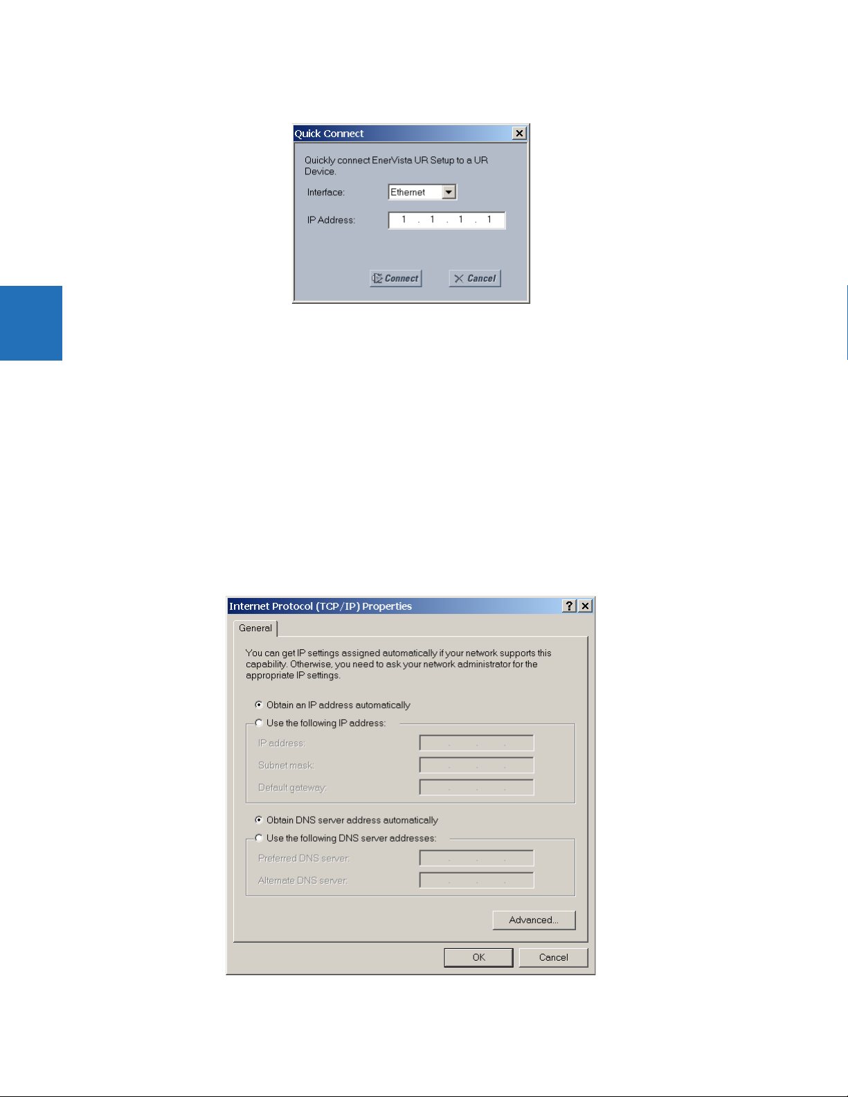
ADD DEVICE TO SOFTWARE CHAPTER 3: INSTALLATION
3. Click the Quick Connect button to open the window.
3
4. Select the Ethernet interface and enter the IP address assigned to the C70, then click the Connect button. The
EnerVista UR Setup software creates a site named “Quick Connect” with a corresponding device also named “Quick
Connect” and displays them on the left side of the screen.
5. Expand the sections to view data directly from the C70 device.
Each time that the EnerVista UR Setup software is initialized, click the Quick Connect button to establish direct
communications to the C70. This ensures that configuration of the EnerVista UR Setup software matches the C70 model
number.
When direct communications with the C70 via Ethernet is complete, make the following changes:
1. From the Windows desktop, right-click the My Network Places icon and select Properties to open the network
connections window.
2. Right-click the Local Area Connection icon and select the Properties item.
3. Select the Internet Protocol (TCP/IP) item from the list provided and click the Properties button.
4. Set the computer to “Obtain a relay address automatically” as shown.
3-52 C70 CAPACITOR BANK PROTECTION AND CONTROL SYSTEM – INSTRUCTION MANUAL
 Loading...