

Page 1
Title page
GE Digital Energy
Multilin
345
Transformer Protection System
Transformer protection and control
SR345 revision: 1.30
Manual P/N: 1601-9099-A1
GE publication code: GEK-113570
Copyright © 2010 GE Multilin
GE Multilin
215 Anderson Avenue, Markham, Ontario
Canada L6E 1B3
Tel: (905) 294-6222 Fax: (905) 201-2098
Internet: http://www.GEmultilin.com
*1601-xxxx-A3*
Communications Guide
GE Multilin's Quality
Management System is
registered to ISO9001:2000
QMI # 005094
Page 2

© 2010 GE Multilin Incorporated. All rights reserved.
GE Multilin SR345 Transformer Protection System Communications Guide for revision 1.30.
SR345 Transformer Protection System, EnerVista, EnerVista Launchpad, and EnerVista SR3
Setup, are registered trademarks of GE Multilin Inc.
The contents of this manual are the property of GE Multilin Inc. This documentation is
furnished on license and may not be reproduced in whole or in part without the permission
of GE Multilin. The content of this manual is for informational use only and is subject to
change without notice.
Part number: 1601-9099-A1 (February 2010)
Page 3

TOC
Table of Contents
Communications interfaces ...................................................................................... 1
RS485 interface............................................................................................................ 2
Electrical Interface ...........................................................................................................................................2
MODBUS Protocol.............................................................................................................................................2
Data Frame Format and Data Rate........................................................................................................ 2
Data Packet Format ....................................................................................................................................... 3
Error Checking................................................................................................................................................... 3
CRC-16 Algorithm............................................................................................................................................ 3
Timing....................................................................................................................................................................4
345 supported functions.............................................................................................................................. 4
DNP protocol settings.....................................................................................................................................5
DNP communication...................................................................................................................................... 5
DNP device profile ........................................................................................................................................... 6
DNP implementation...................................................................................................................................... 8
DNP serial EnerVista Setup........................................................................................................................13
DNP general .....................................................................................................................................................15
IEC 60870-5-103 serial communication............................................................................................. 16
Interoperability ............................................................................................................................................... 16
Physical layer...................................................................................................................................................16
Link layer ........................................................................................................................................................... 17
Application layer ............................................................................................................................................ 17
Transmission mode for application data............................................................................................17
Common address of ASDU........................................................................................................................17
Selection of standard information numbers in monitor direction..........................................17
Selection of standard information numbers in control direction............................................20
Basic application functions.......................................................................................................................20
Miscellaneous..................................................................................................................................................21
Application level............................................................................................................................................. 21
Application functions...................................................................................................................................21
Type identification.........................................................................................................................................21
Function type...................................................................................................................................................22
Information number.....................................................................................................................................22
Data management ....................................................................................................................................... 22
Digital states ....................................................................................................................................................23
Measurands......................................................................................................................................................23
Commands....................................................................................................................................................... 24
103 general settings ....................................................................................................................................25
Ethernet interface .....................................................................................................26
SNTP.....................................................................................................................................................................26
SNTP settings...................................................................................................................................................26
SNTP modes .....................................................................................................................................................26
MODBUS TCP/IP.............................................................................................................................................. 27
Data and control functions.......................................................................................................................27
Exception and error responses...............................................................................................................35
Request response sequence ....................................................................................................................35
CRC .......................................................................................................................................................................36
DNP Ethernet protocol settings .............................................................................................................. 38
DNP communication....................................................................................................................................38
DNP device profile .........................................................................................................................................38
DNP port allocation.......................................................................................................................................41
DNP implementation....................................................................................................................................42
DNP Ethernet EnerVista Setup.................................................................................................................47
DNP general .....................................................................................................................................................49
IEC60870-5-104 protocol .......................................................................................................................... 50
IEC 60870-5-104 interoperability...........................................................................................................50
345 TRANSFORMER PROTECTION SYSTEM – COMMUNICATIONS GUIDE toc–1
Page 4

IEC 60870-5-104 protocol settings........................................................................................................58
IEC 60870-5-104 point lists.......................................................................................................................58
Summary of Ethernet client connections ...........................................................................................60
IEC 61850 GOOSE communications......................................................................................................62
EnerVista SR3 Setup software structure.............................................................................................62
GOOSE transmission.....................................................................................................................................64
GOOSE Rx...........................................................................................................................................................65
GOOSE Rx status ............................................................................................................................................66
GOOSE Rx headers........................................................................................................................................67
GOOSE receive dataset structure...........................................................................................................68
GOOSE remote inputs..................................................................................................................................69
USB interface..............................................................................................................72
MODBUS Protocol ..........................................................................................................................................72
Data Frame Format and Data Rate......................................................................................................72
Data Packet Format......................................................................................................................................72
Error Checking.................................................................................................................................................73
CRC-16 Algorithm ..........................................................................................................................................73
Timing..................................................................................................................................................................74
345 supported functions............................................................................................................................74
MODBUS memory map.............................................................................................75
Format Codes ...............................................................................................................................................128
MODBUS Functions ................................................................................................ 171
Function Code 03H.....................................................................................................................................171
Function Code 04H.....................................................................................................................................171
Function Code 05H.....................................................................................................................................172
Function Code 06H.....................................................................................................................................173
Function Code 07H.....................................................................................................................................173
Function Code 08H.....................................................................................................................................174
Function Code 10H.....................................................................................................................................175
Error Responses........................................................................................................................................... 175
Force coil commands................................................................................................................................176
Performing Commands Using Function Code 10H.....................................................................177
Using the MODBUS User Map............................................................................... 179
MODBUS User Map.....................................................................................................................................179
TOC
toc–2 345 TRANSFORMER PROTECTION SYSTEM – COMMUNICATIONS GUIDE
Page 5

Digital Energy
Multilin
345 Transformer Protection System
Communications Guide
Communications Guide
Communications interfaces
The 345 has three communications interfaces. These can be used simultaneously:
• RS485
•USB
•Ethernet
345 TRANSFORMER PROTECTION SYSTEM – COMMUNICATIONS GUIDE 1–1
Page 6

RS485 INTERFACE CHAPTER 1: COMMUNICATIONS GUIDE
NOTE
NOTE
RS485 interface
The hardware or electrical interface in the 345 is two-wire RS485. In a two-wire link, data is
transmitted and received over the same two wires. Although RS485 two wire
communication is bi-directional, the data is never transmitted and received at the same
time. This means that the data flow is half duplex.
NOTE:
Electrical Interface
NOTE:
Polarity is important in RS485 communications. The '+' (positive) terminals of every device
must be connected together.
The hardware or electrical interface in the 345 is two-wire RS485. In a two-wire link, data is
transmitted and received over the same two wires. Although RS485 two wire
communication is bi-directional, the data is never transmitted and received at the same
time. This means that the data flow is half duplex.
RS485 lines should be connected in a daisy chain configuration with terminating networks
installed at each end of the link (i.e. at the master end and at the slave farthest from the
master). The terminating network should consist of a 120 W resistor in series with a 1 nF
ceramic capacitor when used with Belden 9841 RS485 wire. Shielded wire should always
be used to minimize noise. The shield should be connected to all of the 345s as well as the
master, then grounded at one location only. This keeps the ground potential at the same
level for all of the devices on the serial link.
Polarity is important in RS485 communications. The '+' (positive) terminals of every device
must be connected together.
MODBUS Protocol
Data Frame Format
and Data Rate
The 345 implements a subset of the Modicon Modbus RTU serial communication standard.
The Modbus protocol is hardware-independent. That is, the physical layer can be any of a
variety of standard hardware configurations. This includes USB, RS485, fibre optics, etc.
Modbus is a single master / multiple slave type of protocol suitable for a multi-drop
configuration.
The 345 is always a Modbus slave. It can not be programmed as a Modbus master.
Computers or PLCs are commonly programmed as masters.
Both monitoring and control are possible using read and write register commands. Other
commands are supported to provide additional functions.
The Modbus protocol has the following characteristics.
•Address: 1 to 254
• Supported Modbus function codes: 3, 4, 5, 6, 7, 8, 10
One data frame of an asynchronous transmission to or from a 345 typically consists of 1
start bit, 8 data bits, and 1 stop bit . This produces a 10 bit data frame. This is important for
transmission through modems at high bit rates.
Modbus protocol can be implemented at any standard communication speed. The 345
supports operation at 9600, 19200, 38400, 57600, and 115200 baud.
1–2 345 TRANSFORMER PROTECTION SYSTEM – COMMUNICATIONS GUIDE
Page 7

CHAPTER 1: COMMUNICATIONS GUIDE RS485 INTERFACE
Data Packet Format A complete request/response sequence consists of the following bytes (transmitted as
separate data frames):
Master Request Transmission:
SLAVE ADDRESS: 1 byte
FUNCTION CODE: 1 byte
DATA: variable number of bytes depending on FUNCTION CODE
CRC: 2 bytes
Slave Response Transmission:
SLAVE ADDRESS: 1 byte
FUNCTION CODE: 1 byte
DATA: variable number of bytes depending on FUNCTION CODE
CRC: 2 bytes
SLAVE ADDRESS: This is the first byte of every transmission. This byte represents the userassigned address of the slave device that is to receive the message sent by the master.
Each slave device must be assigned a unique address and only the addressed slave will
respond to a transmission that starts with its address. In a master request transmission the
SLAVE ADDRESS represents the address of the slave to which the request is being sent. In a
slave response transmission the SLAVE ADDRESS represents the address of the slave that is
sending the response.
FUNCTION CODE: This is the second byte of every transmission. Modbus defines function
codes of 1 to 127.
DATA: This will be a variable number of bytes depending on the FUNCTION CODE. This may
be Actual Values, Setpoints, or addresses sent by the master to the slave or by the slave to
the master.
CRC: This is a two byte error checking code.
Error Checking The RTU version of Modbus includes a two byte CRC-16 (16 bit cyclic redundancy check)
with every transmission. The CRC-16 algorithm essentially treats the entire data stream
(data bits only; start, stop and parity ignored) as one continuous binary number. This
number is first shifted left 16 bits and then divided by a characteristic polynomial
(11000000000000101B). The 16 bit remainder of the division is appended to the end of the
transmission, MSByte first. The resulting message including CRC, when divided by the
same polynomial at the receiver will give a zero remainder if no transmission errors have
occurred.
If a 345 Modbus slave device receives a transmission in which an error is indicated by the
CRC-16 calculation, the slave device will not respond to the transmission. A CRC-16 error
indicates than one or more bytes of the transmission were received incorrectly and thus
the entire transmission should be ignored in order to avoid the 345 performing any
incorrect operation.
The CRC-16 calculation is an industry standard method used for error detection. An
algorithm is included here to assist programmers in situations where no standard CRC-16
calculation routines are available.
CRC-16 Algorithm Once the following algorithm is complete, the working register “A” will contain the CRC
value to be transmitted. Note that this algorithm requires the characteristic polynomial to
be reverse bit ordered. The MSBit of the characteristic polynomial is dropped since it does
not affect the value of the remainder. The following symbols are used in the algorithm:
—>: data transfer
A: 16 bit working register
AL: low order byte of A
AH: high order byte of A
CRC: 16 bit CRC-16 value
345 TRANSFORMER PROTECTION SYSTEM – COMMUNICATIONS GUIDE 1–3
Page 8

RS485 INTERFACE CHAPTER 1: COMMUNICATIONS GUIDE
i, j: loop counters
(+): logical exclusive or operator
Di: i-th data byte (i = 0 to N-1)
G: 16 bit characteristic polynomial = 1010000000000001 with MSbit dropped and bit order
reversed
shr(x): shift right (the LSbit of the low order byte of x shifts into a carry flag, a '0' is shifted
into the MSbit of the high order byte of x, all other bits shift right one location
The algorithm is:
1. FFFF hex —> A
2. 0 —> i
3. 0 —> j
4. Di (+) AL —> AL
5. j+1 —> j
6. shr(A)
7. is there a carry? No: go to 8. Yes: G (+) A —> A
Timing Data packet synchronization is maintained by timing constraints. The receiving device
345 supported
functions
8. is j = 8? No: go to 5. Yes: go to 9.
9. i+1 —> i
10. is i = N? No: go to 3. Yes: go to 11.
11. A —> CRC
must measure the time between the reception of characters. If 3.5 character times elapse
without a new character or completion of the packet, then the communication link must
be reset (i.e. all slaves start listening for a new transmission from the master). Thus at 9600
baud a delay of greater than 3.5 x 1 / 9600 x 10 x = x 3.65 x ms will cause the
communication link to be reset.
The following functions are supported by the 345:
• FUNCTION CODE 03 - Read Setpoints
• FUNCTION CODE 04 - Read Actual Values
• FUNCTION CODE 05 - Execute Operation
• FUNCTION CODE 06 - Store Single Setpoint
• FUNCTION CODE 07 - Read Device Status
• FUNCTION CODE 08 - Loopback Test
• FUNCTION CODE 10 - Store Multiple Setpoints
Refer to section 5 of this guide for more details on MODBUS function codes.
1–4 345 TRANSFORMER PROTECTION SYSTEM – COMMUNICATIONS GUIDE
Page 9

CHAPTER 1: COMMUNICATIONS GUIDE RS485 INTERFACE
S1 DNP GENERAL
DNP ADDRESS
DNP TCP/UDP PORT
CHANNEL 1 PORT
CHANNEL 2 PORT
TME SYNC IIN PER.
DNP MSG FRAG SIZE
DNP TCP CONN. T/O
▼
S1 DNP
DNP GENERAL
DNP UNSOL RESPONSE*
DEFAULT VARIATION
DNP CLIENT ADDRESS*
DNP POINTS LIST
897769.cdr
DNP CLIENT ADDRESS*
CLIENT ADDRESS 1
CLIENT ADDRESS 2
CLIENT ADDRESS 3
CLIENT ADDRESS 4
CLIENT ADDRESS 5
POINT 0
...
POINT 1
POINT 2
POINT 63
▼
S1 DNP POINTS LIST
BINARY INPUTS
BINARY OUTPUT
ANALOG INPUTS
POINT 0 ENTRY
...
POINT 1 ENTRY
POINT 31 ENTRY
▼
POINT 0 ON
...
POINT 0 OFF
POINT 1 ON
POINT 1 OFF
POINT 15 ON
POINT 15 OFF
▼
DEFAULT VARIATION
DNP OBJECT 1
DNP OBJECT 2
DNP OBJECT 20
DNP OBJECT 21
DNP OBJECT 22
DNP OBJECT 23
DNP OBJECT 30
DNP OBJECT 32
DNP UNSOL RESPONSE*
FUNCTION
▼
TIMEOUT
MAX RETRIES
DEST ADDRESS
* Ethernet only
DNP protocol settings
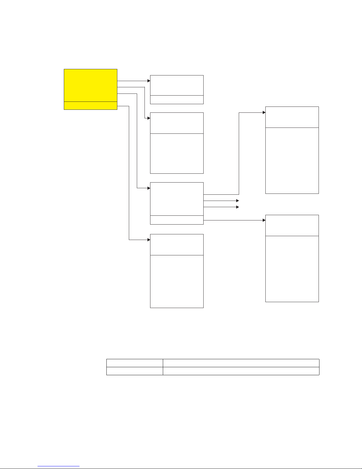
DNP communication The menu structure for the DNP protocol is shown below.
The following path is available using the keypad. For instructions on how to use the
keypad, please refer to Chapter 3 - Working with the Keypad.
PATH:
SETPOINTS > RELAY SETUP > COMMUNICATIONS > DNP PROTOCOL > DNP GENERAL
345 TRANSFORMER PROTECTION SYSTEM – COMMUNICATIONS GUIDE 1–5
Page 10

RS485 INTERFACE CHAPTER 1: COMMUNICATIONS GUIDE
DNP device profile
DNP 3.0 Device Profile
(Also see the IMPLEMENTATION TABLE in the following section)
Vendor Name: General Electric Multilin
Device Name: SR345 Relay
Highest DNP Level Supported:
For Requests: Level 2
For Responses: Level 2
Device Function:
□ Master
⊠ Slave
Notable objects, functions, and/or qualifiers supported in addition to the Highest DNP Levels
Supported (the complete list is described in the attached table):
Binary Inputs (Object 1)
Binary Input Changes (Object 2)
Binary Outputs (Object 10)
Control Relay Output Block (Object 12)
Binary Counters (Object 20)
Frozen Counters (Object 21)
Counter Change Event (Object 22)
Frozen Counter Event (Object 23)
Analog Inputs (Object 30)
Analog Input Changes (Object 32)
Analog Deadbands (Object 34)
Time and Date (Object 50)
Internal Indications (Object 80)
Maximum Data Link Frame Size (octets): Maximum Application Fragment Size (octets):
Transmitted: 292 Transmitted: configurable up to 2048
Received: 292 Received: 2048
Maximum Data Link Re-tries: Maximum Application Layer Re-tries:
⊠None ⊠ None
□Fixed at 3 □ Configurable
□Configurable
Requires Data Link Layer Confirmation:
⊠ Never
□ Always
□ Sometimes
□ Configurable
Requires Application Layer Confirmation:
□ Never
□ Always
1–6 345 TRANSFORMER PROTECTION SYSTEM – COMMUNICATIONS GUIDE
Page 11

CHAPTER 1: COMMUNICATIONS GUIDE RS485 INTERFACE
DNP 3.0 Device Profile
⊠ When reporting Event Data
⊠ When sending multi-fragment responses
□ Sometimes
□ Configurable
Timeouts while waiting for:
Data Link Confirm: ⊠ None □ Fixed □ Variable □ Configurable
Complete Appl. Fragment: ⊠ None □ Fixed □ Variable □ Configurable
Application Confirm: □ None ⊠ Fixed at 10 s □ Variable □ Configurable
Complete Appl. Response: ⊠ None □ Fixed at ___ □ Variable □ Configurable
Others:
Transmission Delay: No intentional delay
Need Time Interval: Configurable (default = 24 hrs.)
Select/Operate Arm Timeout: 10 s
Binary input change scanning period: 8 times per power system cycle
Analog input change scanning period: 500 ms
Counter change scanning period: 500 ms
Frozen counter event scanning period: 500 ms
Sends/Executes Control Operations:
WRITE Binary Outputs ⊠ Never □ Always □ Sometimes □Configurable
SELECT/OPERATE □ Never ⊠ Always
□ Sometimes □ Configurable
DIRECT OPERATE □ Never ⊠Always □ Sometimes □ Configurable
DIRECT OPERATE – NO ACK □ Never ⊠ Always □ Sometimes □ Configurable
Count > 1 ⊠ Never □ Always □ Sometimes □ Configurable
Pulse On □ Never □ Always ⊠ Sometimes □ Configurable
Pulse Off □ Never □ Always ⊠ Sometimes □ Configurable
Latch On □ Never □ Always ⊠ Sometimes □ Configurable
Latch Off □ Never □ Always ⊠ Sometimes □ Configurable
Queue ⊠ Never □ Always □ Sometimes □ Configurable
Clear Queue ⊠ Never
□ Always □ Sometimes □ Configurable
Explanation of ‘Sometimes’: Object 12 points are mapped to Virtual Inputs. Both “Pulse On” and
“Latch On” operations perform the same function in the 345; that is, the appropriate Virtual Input is
put into the “On” state. The On/Off times and Count value are ignored. “Pulse Off” and “Latch Off”
operations put the appropriate Virtual Input into the “Off” state.
Reports Binary Input Change Events when no
specific variation requested:
Reports time-tagged Binary Input Change
Events when no specific variation
requested:
□ Never □ Never
⊠ Only time-tagged ⊠ Binary Input Change With Time
□ Only non-time-tagged □ Binary Input Change With Relative Time
□ Configurable □ Configurable (attach explanation)
Sends Unsolicited Responses: Sends Static Data in Unsolicited Responses:
□ Never ⊠ Never
□ Configurable □ When Device Restarts
□ Only certain objects □ When Status Flags Change
⊠ Sometimes No other options are permitted.
⊠ ENABLE/DISABLE unsolicited Function codes
supported
345 TRANSFORMER PROTECTION SYSTEM – COMMUNICATIONS GUIDE 1–7
Page 12

RS485 INTERFACE CHAPTER 1: COMMUNICATIONS GUIDE
DNP 3.0 Device Profile
Explanation of ‘Sometimes’: It will be disabled for
RS-485 applications, since there is no collision
avoidance mechanism. For Ethernet communication
it will be available and it can be disabled or enabled
with the proper function code.
Default Counter Object/Variation: Counters Roll Over at:
□ No Counters Reported □ No Counters Reported
□ Configurable (attach explanation) □ Configurable (attach explanation)
⊠ Default Object: 20 ⊠ 16 Bits
Default Variation: 1
⊠ Point-by-point list attached □ Other Value: _____
⊠ Point-by-point list attached
Sends Multi-Fragment Responses:
⊠ Yes
□ No
DNP implementation Table 1: DNP Implementation
OBJECT REQUEST RESPONSE
OBJECT
NO.
1 0 Binary Input (Variation 0
2 0 Binary Input Change
10 0 Binary Output Status
VARIATION
NO.
1 Binary Input 1 (read) 22
2 Binary Input with Status 1 (read) 22
1 Binary Input Change
2 Binary Input Change
3 Binary Input Change
DESCRIPTION FUNCTION
is used to request
default variation)
(Variation 0 is used to
request default
variation)
without Time
with Time
with Relative Time
(Variation 0 is used to
request default
variation)
CODES
(DEC)
1 (read) 22
(assign
class)
(assign
class)
(assign
class)
1 (read) 06 (no range, or all)
1 (read) 06 (no range, or all)
1 (read) 06 (no range, or all)
1 (read) 06 (no range, or all)
1 (read) 00, 01(start-stop)
QUALIFIER CODES
(HEX)
00, 01 (start-stop)
06 (no range, or all)
07, 08 (limited
quantity) 17, 28
(index)
00, 01 (start-stop)
06 (no range, or all)
07, 08 (limited
quantity) 17, 28
(index)
00, 01 (start-stop)
06 (no range, or all)
07, 08 (limited
quantity) 17, 28
(index)
07, 08 (limited
quantity)
07, 08 (limited
quantity)
07, 08 (limited
quantity)
07, 08 (limited
quantity)
06 (no range, or all)
07, 08 (limited
quantity) 17, 28
(index)
FUNCTION
CODES
(DEC)
--- ---
129
(response)
129
(response)
--- ---
129
(response)
130 (unsol.
resp.)
129
(response)
130 (unsol.
resp.)
--- ---
--- ---
QUALIFIER
CODES
(HEX)
00, 01
(start-stop)
17, 28
(index) (see
Note 2)
00, 01
(start-stop)
17, 28
(index) (see
Note 2)
17, 28
(index)
17, 28
(index)
1–8 345 TRANSFORMER PROTECTION SYSTEM – COMMUNICATIONS GUIDE
Page 13

CHAPTER 1: COMMUNICATIONS GUIDE RS485 INTERFACE
OBJECT REQUEST RESPONSE
OBJECT
NO.
12 1 Control Relay Output
VARIATION
NO.
DESCRIPTION FUNCTION
CODES
QUALIFIER CODES
(HEX)
(DEC)
2 Binary Output Status 1 (read) 00, 01 (start-stop)
06 (no range, or all)
07, 08 (limited
quantity) 17, 28
(index)
Block
3 (select)4
(operate) 5
(direct op) 6
(dir. op,
00, 01 (start-stop)
07, 08 (limited
quantity) 17, 28
(index)
FUNCTION
CODES
(DEC)
129
(response)
129
(response)
QUALIFIER
CODES
(HEX)
00, 01
(start-stop)
17, 28
(index) (see
Note 2)
echo of
request
noack)
20 0 Binary Counter
(Variation 0 is used to
request default
variation)
1 (read) 7
(freeze) 8
(freeze
noack) 9
(freeze clear)
00, 01 (start-stop)
06 (no range, or all)
07, 08 (limited
quantity) 17, 28
(index)
--- ---
10 (frz. cl.
noack) 22
(assign
class)
1 32-Bit Binary Counter 1 (read)7
(freeze) 8
(freeze
noack) 9
(freeze clear)
00, 01 (start-stop)
06 (no range, or all)
07, 08 (limited
quantity) 17, 28
(index)
129
(response)
00, 01
(start-stop)
17, 28
(index) (see
Note 2)
10 (frz. cl.
noack) 22
(assign
class)
2 16-Bit Binary Counter 1 (read) 7
(freeze) 8
(freeze
noack) 9
(freeze clear)
00, 01 (start-stop)
06 (no range, or all)
07, 08 (limited
quantity) 17, 28
(index)
129
(response)
00, 01
(start-stop)
17, 28
(index) (see
Note 2)
10 (frz. cl.
noack) 22
(assign
class)
5 32-Bit Binary Counter
without Flag
1 (read) 7
(freeze) 8
(freeze
noack) 9
(freeze clear)
00, 01 (start-stop)
06 (no range, or all)
07, 08 (limited
quantity) 17, 28
(index)
129
(response)
00, 01
(start-stop)
17, 28
(index) (see
Note 2)
10 (frz. cl.
noack) 22
(assign
class)
6 16-Bit Binary Counter
without Flag
1 (read) 7
(freeze) 8
(freeze
noack) 9
(freeze clear)
00, 01 (start-stop)
06 (no range, or all)
07, 08 (limited
quantity) 17, 28
(index)
129
(response)
00, 01
(start-stop)
17, 28
(index) (see
Note 2)
10 (frz. cl.
noack) 22
(assign
class)
21 0 Frozen
Counter(Variation 0 is
used to request
defaultvariation)
1 (read) 22
(assign
class)
00, 01 (start-stop)
06 (no range, or all)
07, 08 (limited
quantity) 17, 28
--- ---
(index)
1 32-Bit Frozen Counter 1 (read) 22
(assign
class)
00, 01 (start-stop)
06 (no range, or all)
07, 08 (limited
quantity) 17, 28
(index)
129
(response)
00, 01
(start-stop)
17, 28
(index) (see
Note 2)
345 TRANSFORMER PROTECTION SYSTEM – COMMUNICATIONS GUIDE 1–9
Page 14

RS485 INTERFACE CHAPTER 1: COMMUNICATIONS GUIDE
OBJECT REQUEST RESPONSE
OBJECT
NO.
22 0 Counter Change Event
VARIATION
NO.
DESCRIPTION FUNCTION
CODES
(DEC)
2 16-Bit Frozen Counter 1 (read) 22
(assign
class)
9 32-Bit Frozen Counter
without Flag
1 (read) 22
(assign
class)
10 16-Bit Frozen Counter
without Flag
1 (read) 22
(assign
class)
1 (read) 06 (no range, or all)
(Variation 0 is used to
request default
QUALIFIER CODES
(HEX)
00, 01 (start-stop)
06 (no range, or all)
07, 08 (limited
quantity) 17, 28
(index)
00, 01 (start-stop)
06 (no range, or all)
07, 08 (limited
quantity) 17, 28
(index)
00, 01 (start-stop)
06 (no range, or all)
07, 08 (limited
quantity) 17, 28
(index)
07, 08 (limited
quantity)
FUNCTION
CODES
(DEC)
129
(response)
QUALIFIER
CODES
(HEX)
00, 01
(start-stop)
17, 28
(index) (see
Note 2)
129
(response)
00, 01
(start-stop)
17, 28
(index) (see
Note 2)
129
(response)
00, 01
(start-stop)
17, 28
(index) (see
Note 2)
--- ---
variation)
1 32-Bit Counter Change
Event
1 (read) 06 (no range, or all)
07, 08 (limited
quantity)
129
(response)
130 (unsol.
17, 28
(index)
resp.)
23 2 16-Bit Counter Change
Event
1 (read) 06 (no range, or all)
07, 08 (limited
quantity)
129
(response)
130 (unsol.
17, 28
(index)
resp.)
5 32-Bit Counter Change
Event with Time
1 (read) 06 (no range, or all)
07, 08 (limited
quantity)
129
(response)
130 (unsol.
17, 28
(index)
resp.)
6 16-Bit Counter Change
Event with Time
1 (read) 06 (no range, or all)
07, 08 (limited
quantity)
129
(response)
130 (unsol.
17, 28
(index)
resp.)
0 Frozen Counter Event
(Variation 0 is used to
request default
1 (read) 06 (no range, or all)
07, 08 (limited
quantity)
--- ---
variation)
1 32-Bit Frozen Counter
Event
1 (read) 06 (no range, or all)
07, 08 (limited
quantity)
129
(response)
130 (unsol.
17, 28
(index)
resp.)
2 16-Bit Frozen Counter
Event
1 (read) 06 (no range, or all)
07, 08 (limited
quantity)
129
(response)
130 (unsol.
17, 28
(index)
resp.)
5 32-Bit Frozen Counter
Event with Time
1 (read) 06 (no range, or all)
07, 08 (limited
quantity)
129
(response)
130 (unsol.
17, 28
(index)
resp.)
6 16-Bit Frozen Counter
Event with Time
1 (read) 06 (no range, or all)
07, 08 (limited
quantity)
129
(response)
130 (unsol.
17, 28
(index)
resp.)
30 0 Analog Input (Variation
0 is used to request
default variation)
1 (read) 22
(assign
class)
00, 01 (start-stop)
06 (no range, or all)
07, 08 (limited
--- ---
quantity) 17, 28
(index)
1–10 345 TRANSFORMER PROTECTION SYSTEM – COMMUNICATIONS GUIDE
Page 15

CHAPTER 1: COMMUNICATIONS GUIDE RS485 INTERFACE
OBJECT REQUEST RESPONSE
OBJECT
NO.
32 0 Analog Change Event
VARIATION
NO.
DESCRIPTION FUNCTION
CODES
(DEC)
1 32-Bit Analog Input 1 (read) 22
(assign
class)
2 16-Bit Analog Input 1 (read) 22
(assign
class)
3 32-Bit Analog Input
without Flag
1 (read) 22
(assign
class)
4 16-Bit Analog Input
without Flag
1 (read) 22
(assign
class)
1 (read) 06 (no range, or all)
(Variation 0 is used to
request default
QUALIFIER CODES
(HEX)
00, 01 (start-stop)
06 (no range, or all)
07, 08 (limited
quantity) 17, 28
(index)
00, 01 (start-stop)
06 (no range, or all)
07, 08 (limited
quantity) 17, 28
(index)
00, 01 (start-stop)
06 (no range, or all)
07, 08 (limited
quantity) 17, 28
(index)
00, 01 (start-stop)
06 (no range, or all)
07, 08 (limited
quantity) 17, 28
(index)
07, 08 (limited
quantity)
FUNCTION
CODES
(DEC)
129
(response)
QUALIFIER
CODES
(HEX)
00, 01
(start-stop)
17, 28
(index) (see
Note 2)
129
(response)
00, 01
(start-stop)
17, 28
(index) (see
Note 2)
129
(response)
00, 01
(start-stop)
17, 28
(index) (see
Note 2)
129
(response)
00, 01
(start-stop)
17, 28
(index) (see
Note 2)
--- ---
variation)
1 32-Bit Analog Change
Event without Time
1 (read) 06 (no range, or all)
07, 08 (limited
quantity)
129
(response)
130 (unsol.
17, 28
(index)
resp.)
2 16-Bit Analog Change
Event without Time
1 (read) 06 (no range, or all)
07, 08 (limited
quantity)
129
(response)
130 (unsol.
17, 28
(index)
resp.)
3 32-Bit Analog Change
Event with Time
1 (read) 06 (no range, or all)
07, 08 (limited
quantity)
129
(response)
130 (unsol.
17, 28
(index)
resp.)
4 16-Bit Analog Change
Event with Time
1 (read) 06 (no range, or all)
07, 08 (limited
quantity)
129
(response)
130 (unsol.
17, 28
(index)
resp.)
34 0 Analog Input Reporting
Deadband (Variation 0 is
used to request
defaultvariation)
1 (read) 00, 01 (start-stop)
06 (no range, or all)
07, 08 (limited
quantity) 17, 28
--- ---
(index)
1 16-bit Analog Input
Reporting Deadband
(default - see Note 1)
1 (read) 00, 01 (start-stop)
06 (no range, or all)
07, 08 (limited
quantity) 17, 28
(index)
2 (write) 00, 01 (start-stop)
129
(response)
00, 01
(start-stop)
17, 28
(index) (see
Note 2)
--- --07, 08 (limited
quantity) 17, 28
(index)
2 32-bit Analog Input
Reporting Deadband
1 (read) 00, 01 (start-stop)
06 (no range, or all)
07, 08 (limited
quantity) 17, 28
(index)
129
(response)
00, 01
(start-stop)
17, 28
(index) (see
Note 2)
345 TRANSFORMER PROTECTION SYSTEM – COMMUNICATIONS GUIDE 1–11
Page 16

RS485 INTERFACE CHAPTER 1: COMMUNICATIONS GUIDE
NOTE
OBJECT REQUEST RESPONSE
OBJECT
NO.
VARIATION
NO.
DESCRIPTION FUNCTION
CODES
(DEC)
2 (write) 00, 01 (start-stop)
QUALIFIER CODES
(HEX)
FUNCTION
CODES
(DEC)
QUALIFIER
CODES
(HEX)
--- --07, 08 (limited
quantity) 17, 28
(index)
50 1 Time and Date (default -
see Note 1)
52 2 Time Delay Fine
(quantity = 1)
60 0 Class 0, 1, 2, and 3 Data 1 (read) 20
1 (read)2
(write)
129
(response)
00, 01 (start-stop)
06 (no range, or all)
07 (limited qty=1) 08
(limited quantity)
17, 28 (index)
129
(response)
00, 01
(start-stop)
17, 28
(index) (see
Note 2)
07 (limited quantity) --- ---
06 (no range, or all) --- ---
(enable
unsol) 21
(disable
unsol) 22
(assign
class)
1 Class 0 Data 1 (read) 22
06 (no range, or all) --- ---
(assign
class)
2 Class 1 Data 1 (read) 20
(enable
unsol)
3 Class 2 Data 21 (disable
06 (no range, or all)
07, 08 (limited
quantity)
--- ---
--- ---
unsol)
4 Class 3 Data 22 (assign
--- ---
class)
80 1 Internal Indications 1 (read) 00, 01 (start-stop)
(index =7)
2 (write) (see
Note 3)
No Object (function
code only) see Note 3
No Object (function
code only)
No Object (function
code only)
NOTE:
1. A default variation refers to the variation response when variation 0 is requested and/
13 (cold
restart)
14 (warm
restart)
23 (delay
meas.)
00 (start-stop)
(index =7)
--- --- ---
--- --- ---
--- --- ---
129
(response)
00, 01
(start-stop)
--- ---
or in class 0, 1, 2, or 3 scans. The default variations for object types 1, 2, 20, 21, 22, 23,
30, and 32 are selected via relay settings. This optimizes the class 0 poll data size.
2. For static (non-change-event) objects, qualifiers 17 or 28 are only responded when a
request is sent with qualifiers 17 or 28, respectively. Otherwise, static object requests
sent with qualifiers 00, 01, 06, 07, or 08, will be responded with qualifiers 00 or 01 (for
changeevent objects, qualifiers 17 or 28 are always responded.)
3. Cold restarts are implemented the same as warm restarts – the 345 is not restarted,
but the DNP process is restarted.
1–12 345 TRANSFORMER PROTECTION SYSTEM – COMMUNICATIONS GUIDE
Page 17

CHAPTER 1: COMMUNICATIONS GUIDE RS485 INTERFACE
DNP serial EnerVista
Setup
The following tables show the settings needed to configure all the DNP 3.0 implementation
parameters.
Table 2: RS-485
SETTINGS PARAMETER RANGE FORMAT
RS485 Baud Rate 115200 9600, 19200, 38400, 57600,
115200
RS485 Comm Parity None None, Odd, Even F102
Rear 485 Protocol DNP 3.0 Modbus, IEC60870-5-103, DNP
3.0
F101
F97
In order to activate DNP 3.0 at the RS485 rear port, the setting "Rear 485 Protocol" must be
set to DNP 3.0. Once the setting has been changed, the relay must be switched off, then
switched on.
Table 3: DNP protocol
SETTINGS PARAMETER RANGE FORMAT
DNP Unsol Resp Function Disabled Disabled ; Enabled F126
DNP Unsol Resp Timeout 5 s 0 to 60 s F1
DNP Unsol Resp Max Retries 10 1 to 255 F1
DNP Unsol Resp Dest Addr 1 0 to 65519 F1
DNP Time Sync IIN Period 1440 min 1 to 10080 min F1
DNP Message Fragment Size 240 30 to 2048 F1
DNP Object 1 Default Variation 2 1 ; 2 F1
DNP Object 2 Default Variation 2 1 ; 2 F1
DNP Object 20 Default Variation 1 1 ; 2 , 5 ; 6 F78
DNP Object 21 Default Variation 1 1 ; 2 ; 9 ; 10 F79
DNP Object 22 Default Variation 1 1 ; 2 , 5 ; 6 F80
DNP Object 23 Default Variation 1 1 ; 2 , 5 ; 6 F81
DNP Object 30 Default Variation 1 1 ; 2 ;3 ; 4 F82
DNP Object 32 Default Variation 1 1 ; 2 ;3 ; 4 F83
DNP TCP Connection Timeout 120 s 10 to 300 s F1
345 TRANSFORMER PROTECTION SYSTEM – COMMUNICATIONS GUIDE 1–13
Page 18

RS485 INTERFACE CHAPTER 1: COMMUNICATIONS GUIDE
Table 4: DNP point list
SETTINGS PARAMETER RANGE FORMAT
Binary Input Point 0 Entry Select entry
from a list
Operands F134
Binary Input Point 63 Entry Select entry
Analog Input Point 0 Entry Select entry
Analog Input Point 0 Scale Factor 1 0.001 ; 0.01 ; 0.1 ; 1 ; 10 ; 100 ;
Analog Input Point 0 Deadband 30000 0 to 100000000 F9
Analog Input Point 31 Entry Select entry
Analog Input Point 31 Scale
Factor
Analog Input Point 31 Deadband 30000 0 to 100000000 F9
Binary Output Point 0 ON Select entry
Binary Output Point 0 OFF Select entry
Binary Output Point 15 ON Select entry
Binary Output Point 15 OFF Select entry
from a list
from a list
from a list
1 0.001 ; 0.01 ; 0.1 ; 1 ; 10 ; 100 ;
from a list
from a list
from a list
from a list
Operands F134
Analog parameters
1000 ; 10000 ; 100000
Analog parameters
1000 ; 10000 ; 100000
Virtual Input 1 to 32 and Force
Coils
Virtual Input 1 to 32 and Force
Coils
Virtual Input 1 to 32 and Force
Coils
Virtual Input 1 to 32 and Force
Coils
F85
F85
F86
F86
F86
F86
• DNP UNSOL RESPONSE FUNCTION should be “Disabled” for RS485 applications, since
there is no collision avoidance mechanism.
• The DNP Time Sync IIN Period setting determines how often the Need Time Internal
Indication (IIN) bit is set by the 345. Changing this time allows the 345 to indicate that
a time synchroniztion command is necessary more or less often
• Various settings have been included to configure Default Variation for the Binary
Inputs, Counters and Analog Inputs Objects. The default variation refers to the
variation response when variation 0 is requested, and/or in class 0, 1, 2, or 3 scans
• Up to 64 Binary Inputs and 32 Analog Input entries can be mapped to an item from a
list of 345 status events and metered values. Status events correspond to Funcion
Code 134B.
• Each Analog Input point Deadband and Scale Factor can be set individually instead of
setting a general deadband or scale for different metering groups. This will avoid scale
and deadband conflicts for different meterings of the same nature.
• Up to 16 Binary/Control Outputs can be configured by selecting a Virtual Input or
Command from a list of 32 Virtual Inputs and Commands (Force Coils). Some legacy
DNP implementations use a mapping of one DNP Binary Output to two physical or
virtual control points. In Order to configure Paired Control Points the source for states
ON and OFF should be set to different Virtual Inputs or Commands.
• The DNP Technical Committee recommends using contiguous point numbers, starting
at 0, for each data type, because some DNP3 Master implementations allocate
contiguous memory from point 0 to the last number for each data type.
1–14 345 TRANSFORMER PROTECTION SYSTEM – COMMUNICATIONS GUIDE
Page 19

CHAPTER 1: COMMUNICATIONS GUIDE RS485 INTERFACE
NOTE:
Binary Inputs are inputs to the Master. Binary Outputs are outputs from the Master.
DNP general Default variations for Object 1, 2 , 20 , 21 , 22 , 23 , 30 and Object 32 will be set by settings
and returned for the object in a response when no specific variation is specified in a Master
request.
Any change in the state of any binary point causes the generation of an event, and
consequently, if configured, an unsolicited response, or it is returned when the Master asks
for it. The same behaviour will be seen when an analog value changes by more than its
configured deadband limit . There can be up to 3 Masters in total, but only one Serial
Master.
The following Default Classes will be fixed for the different blocks of data:
Binary Input Points Default Class = 1
Analog Input Point Default Class = 2
Counters Default Class = 3
Each Data Point Class can be changed by protocol function code 22 in volatile mode. If a
restart is performed, the new values will be lost.
DNP Object 34 points can be used to change deadband values from the default for each
individual DNP Analog Input point. These new deadbands will be maintained such that in
the case of a relay restart, the values are not lost.
Requests for Object 20 (Binary Counters), Object 21 (Frozen Counters), and Object 22
(Counter Change Events) must be accepted.
Function codes “Immediate Freeze”, “Freeze and Clear” etc. are accepted as well.
345 TRANSFORMER PROTECTION SYSTEM – COMMUNICATIONS GUIDE 1–15
Page 20
RS485 INTERFACE CHAPTER 1: COMMUNICATIONS GUIDE
S1 103 FIRST ASDU
ID TYPE
FUNCTION TYPE
INFORMATION NO
SCAN TIMEOUT
FIRST ANLG ENTRY
FIRST ANLG FACTOR
FIRST ANLG OFFSET
...
NINTH ANLG ENTRY
NINTH ANLG FACTOR
NINTH ANLG OFFSET
▼
S1 103 GENERAL
SLAVE ADDRESS
SYNCH TIMEOUT
▼
897770.cdr
S1 103 MEASURANDS
FIRST ASDU
SECOND ASDU
THIRD ASDU
FOURTH ASDU
▼
S1 60870-5-103
GENERAL
BINARY INPUTS
MEASURANDS
COMMANDS
▼
S1 103 COMMANDS
CMD 0 FUNC TYPE
CMD 0 INFO NO:
CMD 0 ON OPER:
CMD 0 OFF OPER:
...
CMD 15 FUNC TYPE:
CMD 15 INFO NO:
CMD 15 ON OPER:
CMD 15 OFF OPER:
▼
S1 103 FOURTH ASDU
ID TYPE
FUNCTION TYPE
INFORMATION NO
SCAN TIMEOUT
FIRST ANLG ENTRY
FIRST ANLG FACTOR
FIRST ANLG OFFSET
...
NINTH ANLG ENTRY
NINTH ANLG FACTOR
NINTH ANLG OFFSET
▼
S1 103 B INPUTS
POINT 0
POINT 0 FUNC TYPE
POINT 0 INFO NO:
...
POINT 63
POINT 63FUNC TYPE
POINT 63 INFO NO:
▼
.
.
.
.
IEC 60870-5-103 serial communication
PATH: SETPOINTS > S1 RELAY SETUP > COMMUNICATIONS > IEC61870-5-103
Interoperability
Physical layer
Electrical interface
⊠ EIA RS-485
32 Number of loads for one protection equipment
1–16 345 TRANSFORMER PROTECTION SYSTEM – COMMUNICATIONS GUIDE
Page 21

CHAPTER 1: COMMUNICATIONS GUIDE RS485 INTERFACE
Optical interface
□ Glass fibre
□ Plastic fibre
□ F-SMA type connector
□ BFOC/2,5 type connector
Transmission speed
⊠? 9600 bits/s
⊠? 19200 bits/s
Link layer
There are no choices for the Link Layer.
Application layer
Transmission mode
for application data
Common address of
ASDU
Selection of standard
information numbers
in monitor direction
Mode 1 (least significant octet first), is used exclusively in this companion standard.
⊠ One COMMON ADDRESS OF ASDU (identical with station address)
More than one COMMON ADDRESS OF ASDU
Table 5: System functions in monitor direction
INF Semantics
⊠ <0> End of general interrogation
⊠ <0> Time synchronization
⊠ <2> Reset FCB
⊠ <3> Reset CU
⊠ <4> Start/restart
⊠ <5> Power on
345 TRANSFORMER PROTECTION SYSTEM – COMMUNICATIONS GUIDE 1–17
Page 22

RS485 INTERFACE CHAPTER 1: COMMUNICATIONS GUIDE
Table 6: Status indications in monitor direction
INF Semantics 345 Identifier 345 Data Text
□ <16> Auto-recloser active
□ <17> Teleprotection active
□ <18> Protection active
□ <19> LED reset
□ <20> Monitor direction blocked
□ <21> Test mode
□ <22> Local parameter setting
□ <23> Characteristic 1
□ <24> Characteristic 2
□ <25> Characteristic 3
□ <26> Characteristic 4
□ <27> Auxiliary input 1
□ <28> Auxiliary input 2
□ <29> Auxiliary input 3
□ <30> Auxiliary input 4
Table 7: Supervision indications in monitor direction
INF Semantics 345 Identifier 345 Data Text
□ <32> Measurand supervision I
□ <33> Measurand supervision V
□ <35> Phase sequence supervision
□ <36> Trip circuit supervision
□ <37> I>> back-up operation
□ <38> VT fuse failure
□ <39> Teleprotection disturbed
□ <46> Group warning
□ <47> Group alarm
Table 8: Earth fault indications in monitor direction
INF Semantics 345 Identifier 345 Data Text
□ INF Semantics 345 Identifier 345 Data Text
□ <48> Earth fault L1
□ <49> Earth fault L2
□ <50> Earth fault L3
□ <51> Earth fault forward, i.e. line
□ <52> Earth fault reverse, i.e. busbar
1–18 345 TRANSFORMER PROTECTION SYSTEM – COMMUNICATIONS GUIDE
Page 23

CHAPTER 1: COMMUNICATIONS GUIDE RS485 INTERFACE
Table 9: Fault indications in monitor direction
INF Semantics 345 Identifier 345 Data Text
□ INF Semantics 345 Identifier 345 Data Text
□ <64> Start / pick-up L1
□ <65> Start / pick-up L2
□ <66> Start / pick-up L3
□ <67> Start / pick-up N
□ <68> General trip
□ <69> Trip L1
□ <70> Trip L2
□ <71> Trip L3
□ <72> Trip I>> (back-up operation)
□ <73> Fault location X in ohms
□ <74> Fault forward / line
□ <75> Fault reverse / busbar
□ <76> Teleprotection signal transmitted
□ <77> Teleprotection signal received
□ <78> Zone 1
□ <79> Zone 2
□ <80> Zone 3
□ <81> Zone 4
□ <82> Zone 5
□ <83> Zone 6
□ <84> General start / pick-up
□ <85> Breaker failure
□ <86> Trip measuring system L1
□ <87> Trip measuring system L2
□ <88> Trip measuring system L3
□ <89> Trip measuring system E
□ <90> Trip I>
□ <91> Trip I>>
□ <92> Trip IN>
□ <93> Trip IN>>
Table 10: Auto-reclosure indications in monitor direction
□ <128> CB ‘on’ by AR
□ <129> CB ‘on’ by long-time AR
□ <130> AR blocked
Table 11: Measurands in monitor direction
□ <144> Measurand I
□ <145> Measurands I, V
□ <146> Measurands I, V, P, Q
□ <147> Measurands In, Ven
□ <148> Measurands IL123, VL123, P, Q, f
345 TRANSFORMER PROTECTION SYSTEM – COMMUNICATIONS GUIDE 1–19
INF Semantics 345 Identifier 345 Data Text
INF Semantics 345 Identifier 345 Data Text
Page 24

RS485 INTERFACE CHAPTER 1: COMMUNICATIONS GUIDE
Table 12: Generic functions in monitor direction
INF Semantics
□ <240> Read headings of all defined groups
□ <241> Read values or attributes of all entries of one group
□ <243> Read directory of a single entry
□ <244> Read value or attribute of a single entry
□ <245> End of general interrogation of generic data
□ <249> Write entry with confirmation
□ <250> Write entry with execution
□ <251> Write entry aborted
Selection of standard
information numbers
in control direction
Table 13: System functions in control direction
INF Semantics
⊠ <0> Initiation of general interrogation
⊠ <0> T ime synchronization
Table 14: General commands in control direction
INF Semantics
□ <16> Auto-recloser on / off
□ <17> Teleprotection on / off
□ <18> Protection on / off
□ <19> LED reset
□ <23> Activate characteristic 1
□ <24> Activate characteristic 2
□ <25> Activate characteristic 3
□ <26> Activate characteristic 4
Table 15: General functions in control direction
INF Semantics
□ <240> Read headings of all defined groups
□ <241> Read values or attributes of all entries of one group
□ <243> Read directory of a single entry
□ <244> Read value or attribute of a single entry
□ <245> General interrogation of generic data
□ <248> Write entry
□ <249> Write entry with confirmation
□ <250> Write entry with execution
□ <251> Write entry abort
Basic application
functions
1–20 345 TRANSFORMER PROTECTION SYSTEM – COMMUNICATIONS GUIDE
□ Test mode
□ Blocking of monitor direction
□ Disturbance data
□ Generic services
□ Private data
Page 25

CHAPTER 1: COMMUNICATIONS GUIDE RS485 INTERFACE
Miscellaneous
Measurand Max. MVAL = times rated value
1,2 or 2,4
Current L1 □⊠
Current L2 □⊠
Current L3 □⊠
Voltage L1-E □□
Voltage L2-E □□
Voltage L3-E □□
Active power P □□
Reactive power Q □□
Frequency f □⊠
Voltage L1-L2 □□
Application level
Application functions The unbalanced transmission mode of the protocol is used to avoid the possibility of more
than one protection device attempting to transmit on the channel at the same time, over
the RS485 port.
Data is transferred to the primary or control station (master) using the “data acquisition by
polling” principle. Cyclically, the master will request class 2 data to the secondary station
(slave).
When slave has class 1 data (high priority) pending, the ACD control bit will be set to 1
demanding the master to request for that data.
Periodically, the master may send a General Interrogation in order to update the complete
database.
The measurands will be sent to the primary station as a response to class 2 request. A
setting (0 to 60 min) is available to configure the desired interval, where 0 means
transmission as fast as possible.
The following functions are supported:
• Initialization
•General Interrogation
•Synchronization
• Commands transmission
Type identification The Type Identification implemented will be:
Information in monitor direction:
Information in control direction:
345 TRANSFORMER PROTECTION SYSTEM – COMMUNICATIONS GUIDE 1–21
TYPE IDENTIFICATION UI8[1..8] <1..255>
<1..31>:= definitions of this companion standard(compatible range)
<32..255>:= for special use (private range)
<1>:= time-tagged message
<3>:= measurands I
<5>:= identification
<6>:= time synchronization
<8>:= general interrogation termination
<9>:= measurands II
<6>:= time synchronization
<7>:= general interrogation
Page 26

RS485 INTERFACE CHAPTER 1: COMMUNICATIONS GUIDE
<20>:= general command
Function type FUNCTION TYPE UI8 [1..8] <0..255>
<0..127>:= private range
<128..129>:= compatible range
<130..143>:= private range
<144..145>:= compatible range
<146..159>:= private range
<160..161>:= compatible range
<162..175>:= private range
<176..177>:= compatible range
<178..191>:= private range
<192..193>:= compatible range
<194..207>:= private range
<208..209>:= compatible range
<210..223>:= private range
<224..225>:= compatible range
<226..239>:= private range
<240..241>:= compatible range
<242..253>:= private range
<254..255>:= compatible range
The 345 relay is identified in this protocol as “overcurrent protection”, so it will use the
Function Type <160> for all the digital and analogues points proposed by the standard and
mapped in this profile. For the other data supported by the device, the customer will have
the capability to use them by setting a number from the private range.
Information number INFORMATION NUMBER := UI8 [1..8] <0..255>
Monitor direction := <0..255>
<0..15>:=system functions
<16..31>:= status
<32..47>:=supervision
<48..63>:=earth fault
<64..127>:=short circuit
<128..143>:=auto-reclosure
<144..159>:=measurands
<160..239>:=not used
<240..255>:=generic functions
Control direction:=<0..255>
<0..15>:=system functions
<16..31>:=general commands
<32..239>:=not used
<240..255>:=generic functions
Data management
The 345 relay supports a fixed profile and data that is configurable using the EnerVista
SR3 Setup program.
The data that can be configured are:
• digital states
1–22 345 TRANSFORMER PROTECTION SYSTEM – COMMUNICATIONS GUIDE
Page 27

CHAPTER 1: COMMUNICATIONS GUIDE RS485 INTERFACE
•measurands
•commands.
Digital states Digital states in the relay may be mapped using the EnerVista SR3 Setup program. By
default, states are mapped to information numbers proposed by the standard, but the
user may delete these mappings if desired.
All the mapped information will be sent as a response to a general interrogation like ASDU
1.
For the other states, the customer can assign:
1. Information Number <1..255>
2. Function Type <0..255>.
Settings Digital Status Information Number Function Type
Point 1 Entry Select entry from list <0 – 255 > <0 – 255 >
….
.…
Point 64 Entry Select entry from list <0 – 255 > <0 – 255 >
This means that for each digital point 3 settings are required.
Example:
Modbus Address Description Value Format
43879 Point 1 Entry Digital Status 0x8242 (Undercurrent Trip) FC134
44223 Point 1 Entry Function Type 160 F1
44224 Point 1 Entry Information Number 144 F1
The “Point Entry Digital Status” reuses the DNP Binary Input 43029, 43030, …
Measurands Some analog points are supported by the 345 relay, with compatible information number
that have been identified in the device profile.
For the other measurands, it is possible to use the EnerVista SR3 Setup to select the
desired point and assign the Identification Type (3 or 9), Function Type <0..255>, and
Information Number <1..255>.
If the user selects Identification Type 3 (ASDU 3) only four measurands are available for
configuration, but if Identif ication Type 9 (ASDU 9) is selected, up to nine measurands can
be sent in the IEC103 slave answer. For each measurand, all metering values that the 345
supports, are available in order to be mapped. There are 3 possible configurable ASDUS.
For example, eDataVab is the index in the Modbus Memory Map.
345 TRANSFORMER PROTECTION SYSTEM – COMMUNICATIONS GUIDE 1–23
Page 28

RS485 INTERFACE CHAPTER 1: COMMUNICATIONS GUIDE
Modbus Address Description Value Format
44384 First ASDU Identification Type 3 or 9 F1
44385 First ASDU Function Type <0 – 255 > F1
44386 First ASDU Information Number < 0 – 255 > F1
44387 First ASDU Scan Timeout < 0 – 1000> secs F1
44388 First ASDU First Analog Entry Vab F1
44389 First ASDU First Analog Factor 1 F3
44390 First ASDU First Analog Offset 0 F1
44391 First ASDU Second Analog Entry Ib F1
44392 First ASDU Second Analog Factor 1 F3
44393 First ASDU Second Analog Offset 0 F1
... ... ... ...
44412 First ASDU Ninth Analog Entry Ib F1
44413 First ASDU Ninth Analog Factor 1 F3
... ... ... ...
44443 Second ASDU Ninth Analogue Entry
44444 Second ASDU Ninth Analogue Factor
44445 Second ASDU Ninth Analogue Offset
... ... ... ...
44446 Third ASDU Identification Type
... … ... ...
44476 Third ASDU Ninth Analogue Offset
In the measurands configuration screen, with each selected measurement, a Factor and
an Offset must be configured.
• The Factor is a multiplier factor.
• The Offset is an offset factor to be applied to the relay measurement to make the final
The factor and offset parameters allow the user to perform different scaling in the relay
measurements. The final measurement sent to the IEC103 master will be: “a*x+b”, where
“x” is the relay measurement, “a” is the multiplier factor and “b” is the offset.
The measurands will be sent to the primary station as a response to a class 2 request.
There is a Timeout configurable with increments of 100 ms, between 0 and 60 min, in order
to configure the desired interval.
Commands
All the commands and virtual inputs are available to be mapped using the EnerVista Setup
program. It is possible to choose the desired command for the ON state and the same or
different command for the OFF state.
The user is able to select the Information Number <1..255> and the Function Type <0..255>
command mappings, but the Identification Type 20 (General Commands) is fixed.++ There
are 32 configurable commands.
In this case it will be necessary to define a new format.
For example, FC500:
measurement calculation to be sent to the master
1–24 345 TRANSFORMER PROTECTION SYSTEM – COMMUNICATIONS GUIDE
Page 29

CHAPTER 1: COMMUNICATIONS GUIDE RS485 INTERFACE
Description Value
Virtual Input 1 0
Virtual Input 2 1
...
Virtual Input 32 31
Reset 32
Open 35
Close 36
Modbus Address Description Value Format
Command 1 Function Type <0 – 255 > F1
Command 1 Information Number < 0 – 255 > F1
Command 1 Operation ON 2 FC500
Command 1 Operation OFF 8 FC500
...
Command 16 Function Type <0 – 255 > F1
Command 16 Information Number < 0 – 255 > F1
Command 16 Operation ON 6 FC500
Command 16 Operation OFF 34 FC500
The “Command Operations ON and OFF” reuse the DNP Binary Outputs 43189, 43190,
…
103 general settings
Number Value Range
Comms Port COM1 Enum[None,Com1]
Slave Address 1 [0..254]
Synchronization Timeout 30 min [0..1440]min
If Comms Port is set to NONE, the IEC 870-5-103 communication protocol will not be
available.
If the user sets a value other than 0 in the Synchronization Timeout setting, when this time
expires without receiving a synchronization message, the Invalid bit will be set in the time
stamp of a time-tagged message.
It is necessary to configure other port settings: Baud Rate, etc.
345 TRANSFORMER PROTECTION SYSTEM – COMMUNICATIONS GUIDE 1–25
Page 30

ETHERNET INTERFACE CHAPTER 1: COMMUNICATIONS GUIDE
Ethernet interface
The Ethernet option for the 345 provides both a 1300 nm optical interface, and a 10/100
auto-negotiating copper interface. To select which interface is active, a MODBUS setpoint
(see below) must be modified:
MODBUS
Address
40191 BE EthernetConnectionType 0 1 1 FC230 0
Hex
Address
Description Min Max Step Function
Code
Factory
Default
SNTP
SNTP settings With SNTP, the device can obtain the clock time over an Ethernet network, acting as an
SNTP client to receive time values from an SNTP server.
SNTP Port configures the ports that the device uses, so it’s necessary to configure it in all
cases.
The relay binds to the first unicast message (see below) received from any server, then
continues operating with the SNTP server in unicast mode. Any further responses from
other SNTP servers are ignored. In the unicast mode of operation the chosen time server
can go offline, in which case it takes about one minute for the device to signal an SNTP
FAIL state and switch again to anycast mode in order to try to find another time server.
SNTP modes Three different modes of SNTP operation are supported. These modes are unicast,
broadcast and anycast.
To use SNTP in unicast mode, the SNTP IP Address must be set to the SNTP server IP
address. Once this address is set and the function setting is “UNICAST”, the device attempts
to obtain time values from the SNTP server. Since many time values are obtained and
averaged, it generally takes 10 seconds until the clock is synchronized with the SNTP
server.
It may take up to 30 seconds for the device to signal an SNTP FAIL state if the server is offline. In this case the main CPU generates an alarm similar to that of the IRIG-B case.
To use SNTP in broadcast mode, set the function setting to “BROADCAST”. The device
listens to SNTP messages sent to "all" the broadcast addresses for the subnet .
The device waits up to eighteen minutes (>1024 seconds) to receive an SNTP broadcast
message before signaling an SNTP FAIL state.
To use SNTP in anycast mode, set the function setting to “ANYCAST”. Anycast mode is
designed for use with a set of cooperating servers whose addresses are not known
beforehand by the client. The device sends a request to a multicast group address
assigned by IANA for SNTP protocol purposes. This address is 224.0.1.1 and a group of
SNTP servers listens to it . Upon receiving such a request, each server sends a unicast
response to the SNTP client.
The relay binds to the first unicast message received from any server, then it continues
operating with the SNTP server in unicast mode. Any further responses from other SNTP
servers are ignored. In the unicast mode of operation, the chosen time server can go
offline, in which case it takes about one minute for the device to signal an SNTP FAIL state
and to switch again to the anycast mode to try to find another time server.
1–26 345 TRANSFORMER PROTECTION SYSTEM – COMMUNICATIONS GUIDE
Page 31

CHAPTER 1: COMMUNICATIONS GUIDE ETHERNET INTERFACE
MODBUS TCP/IP
This section describes the procedure to read and write data in the 350 relay using MODBUS
TCP protocol. The MODBUS communication allows the 350 relay to be connected to a
supervisor program or any other device with a master MODBUS communication channel.
The 350 will be always a slave station.
MODBUS TCP is a variant of the MODBUS protocol, intended for supervision and control of
automation equipment. It covers the use of MODBUS messaging in an 'Intranet' or
'Internet' environment using the TCP/IP protocols.
MODBUS TCP basically embeds a MODBUS frame into a TCP frame in a simple manner. This
is a connection-oriented transaction which means that every query expects a response.
When the relay communicates using MODBUS TCP, it does not require a checksum
calculation of the MODBUS frame as does the MODBUS RTU.
The 350 relay supports only a subset of the MODBUS protocol functions.
Data and control
functions
The following functions are supported:
01H Read Coil Status
Just respond, no action required for now.
Outgoing message for this function is the same as input one.
02H Read Input Status
Just respond, no action required for now.
Outgoing message for this function is the same as input one.
03H Read Holding Registers
Reads the binary contents of holding registers in the slave.
Query:
The query message specifies the starting register and quantity of registers to be read.
Registers are addressed starting at zero: registers 1 to 16 are addressed as 0 to 15.
Here is an example of a request to read registers 40172 to 40175 from slave device 254:
Field Name Hex
Slave Address FE
Function 03
Starting Address Hi 00
Starting Address Lo AB
No. of Points Hi 00
No. of Points Lo 04
Response:
The register data in the response message are packed as two bytes per register, with the
binary contents right justified within each byte. For each register, the first byte contains the
high order bits and the second contains the low order bits.
The response is returned when the data is completely assembled.
345 TRANSFORMER PROTECTION SYSTEM – COMMUNICATIONS GUIDE 1–27
Page 32

ETHERNET INTERFACE CHAPTER 1: COMMUNICATIONS GUIDE
Field Name Hex
Slave Address FE
Function 03
Byte Count 08
Data Hi (Register 40172) 00
Data Lo (Register 40172) FE
Data Hi (Register 40173) 00
Data Lo (Register 40173) 04
Data Hi (Register 40174) 00
Data Lo (Register 40174) 00
Data Hi (Register 40175) 00
Data Lo (Register 40175) 00
The contents of register 40172 are shown as the two byte values of 00 FE hex, or254
decimal. The contents of registers 40173 to 40175 are 00 04, 00 00 and 00 00 hex, or4, 0
and 0 decimal.
04H Read Input Registers
Reads the binary contents of input registers (3X references) in the slave.
Query:
The query message specifies the starting register and quantity of registers to be read.
Registers are addressed starting at zero: registers 1 to 16 are addressed as 0 to 15.
Here is an example of a request to read register 30305 from slave device 254:
Field Name Hex
Slave Address FE
Function 04
Starting Address Hi 01
Starting Address Lo 30
No. of Points Hi 00
No. of Points Lo 01
Response:
The register data in the response message are packed as two bytes per register, with the
binary contents right justified within each byte. For each register, the first byte contains the
high order bits and the second contains the low order bits.
Field Name Hex
Slave Address FE
Function 04
Byte Count 02
Data Hi (Register 30305) 80
Data Lo (Register 30305) 80
05H Force Single Coil
Forces a single coil (0X reference) to either ON or OFF.
The query message specifies the coil reference to be forced. Coils are addressed starting at
zero: coil 1 is addressed as 0.
The reguested ON/OFF state is specified by a constant in the query data field.
1–28 345 TRANSFORMER PROTECTION SYSTEM – COMMUNICATIONS GUIDE
Page 33

CHAPTER 1: COMMUNICATIONS GUIDE ETHERNET INTERFACE
A value of FF 00 hex requests the coil to be ON. A value of 00 00 requests it to be OFF. All
other values are illegal and will not affect the coil.
Force Virtual Inputs:
Description Coil Address (HEX) Description Coil Address (HEX)
Virtual Input 1 0x1000 Virtual Input 17 0x1010
Virtual Input 2 0x1001 Virtual Input 18 0x1011
Virtual Input 3 0x1002 Virtual Input 19 0x1012
Virtual Input 4 0x1003 Virtual Input 20 0x1013
Virtual Input 5 0x1004 Virtual Input 21 0x1014
Virtual Input 6 0x1005 Virtual Input 22 0x1015
Virtual Input 7 0x1006 Virtual Input 23 0x1016
Virtual Input 8 0x1007 Virtual Input 24 0x1017
Virtual Input 9 0x1008 Virtual Input 25 0x1018
Virtual Input 10 0x1009 Virtual Input 26 0x1019
Virtual Input 11 0x100A Virtual Input 27 0x101A
Virtual Input 12 0x100B Virtual Input 28 0x101B
Virtual Input 13 0x100C Virtual Input 29 0x101C
Virtual Input 14 0x100D Virtual Input 30 0x101D
Virtual Input 15 0x100E Virtual Input 31 0x101E
Virtual Input 16 0x100F Virtual Input 32 0x101F
Commands:
Description Coil Address (DEC)
eCmdNone 0
eCmdReset 1
eCmdLockoutReset 2
eCmdStop 3
eCmdOpen 4
eCmdClose 5
eCmdDisplayMessage 6
eCmdChangeToSetpointGroup1 7
eCmdChangeToSetpointGroup2 8
eCmdChangeToSetpointGroup3 9
eCmdChangeToSetpointGroup4 10
eCmdCO1_ON 32
eCmdCO1_ON 32
eCmdCO1_Off 33
eCmdCO2_On 34
eCmdCO2_Off 35
eCmdCO3_On 36
eCmdCO3_Off 37
eCmdCO4_On 38
eCmdCO4_Off 39
eCmdCO5_On 40
eCmdCO5_Off 41
345 TRANSFORMER PROTECTION SYSTEM – COMMUNICATIONS GUIDE 1–29
Page 34

ETHERNET INTERFACE CHAPTER 1: COMMUNICATIONS GUIDE
Description Coil Address (DEC)
eCmdCO6_On 42
eCmdCO6_Off 43
eCmdCO7_On 44
eCmdCO7_Off 45
eCmdCO8_On 46
eCmdCO8_Off 47
eCmdCO9_On 48
eCmdCO9_Off 49
eCmdCO10_On 50
eCmdCO10_Off 51
eCmdCO11_On 52
eCmdCO11_Off 53
eCmdCO12_On 54
eCmdCO12_Off 55
eCmdCO13_On 56
eCmdCO13_Off 57
eCmdCO14_On 58
eCmdCO14_Off 59
eCmdCO15_On 60
eCmdCO15_Off 61
eCmdCO16_On 62
eCmdCO16_Off 63
eCmdCO17_On 64
eCmdCO17_Off 65
eCmdCO18_On 66
eCmdCO18_Off 67
eCmdCO19_On 68
eCmdCO19_Off 69
eCmdCO20_On 70
eCmdCO20_Off 71
eCmdCO21_On 72
eCmdCO21_Off 73
eCmdCO22_On 74
eCmdCO22_Off 75
eCmdCO23_On 76
eCmdCO23_Off 77
eCmdCO24_On 78
eCmdCO24_Off 79
eCmdCO25_On 80
eCmdCO25_Off 81
eCmdCO26_On 82
eCmdCO26_Off 83
eCmdCO27_On 84
eCmdCO27_Off 85
eCmdCO28_On 86
eCmdCO28_Off 87
eCmdCO29_On 88
1–30 345 TRANSFORMER PROTECTION SYSTEM – COMMUNICATIONS GUIDE
Page 35

CHAPTER 1: COMMUNICATIONS GUIDE ETHERNET INTERFACE
Description Coil Address (DEC)
eCmdCO29_Off 89
eCmdCO30_On 90
eCmdCO30_Off 91
eCmdCO31_On 92
eCmdCO31_Off 93
eCmdCO32_On 94
eCmdCO32_Off 95
CmdClearTripData 96
eCmdResetPowerMeters 97
eCmdClearDemand 98
eCmdClearCounters 99
eCmdClearEvents 100
eCmdClearWaveform 101
eCmdClearMaintenanceTimer 102
eCmdClearDataLogger 103
eCmdClearTemperatureHistory 104
eCmdClearThermal_Image 105
eCmdRTDMaximums 112
eCmdResetMotorInfo 113
eCmdAutoMode 114
eCmdManualMode 115
eCmdManualInhibit 116
eCmdManualRestore 117
eCmdStartInhibit 118
eCmdStartRestore 119
eCmdTriggerWaveform 120
eCmdStartDataLog 121
eCmdStopDatalog 122
eCmdTempResetIntValues 123
eCmdTempFactoryClear 124
eCmdTempFactoryStoreSample 125
eCmdClearSecurityLog 126
eCmdStartUploadingSetpointFile 127
eCmdEndUploadingSetpointFile 128
eCmdForceLEDs 140
eCMDNoKeyPress 141
eCMDNavUpKey 142
eCMDNavLeftKey 143
eCMDNavDownKey 144
eCMDNavRightKey 145
eCMDUpKey 146
eCMDDownKey 147
eCMDEnterKey 148
eCMDMenuKey 149
eCMDEscapeKey 150
eCMDResetKey 151
eCmdUploadModeEntry2 159
345 TRANSFORMER PROTECTION SYSTEM – COMMUNICATIONS GUIDE 1–31
Page 36

ETHERNET INTERFACE CHAPTER 1: COMMUNICATIONS GUIDE
Description Coil Address (DEC)
eCmdUploadModeEntry1 160
eCmdReloadFactorySetpts2 161
eCmdReloadFactorySetpts1 162
eCmdSecurityMin 163
eCmdFactoryUse1 164
eCmdFactoryUse2 165
eCmdFactoryUse3 166
eCmdFactoryUse4 167
eCmdFactoryUse5 168
eCmdFactoryUse6 169
eCmdFactoryUse7 170
eCmdFactoryUse8 171
eCmdFactoryUse9 172
eCmdFactoryUse10 173
eCmdPaintGCPRed 174
eCmdPaintGCPGreen 175
eCmdPaintGCPBlue 176
eCmdReboot2 177
eCmdReboot1 178
eCmdMAC2 179
eCmdMAC1 180
eCmdCalOffsets2 181
Query:
Here is an example of a request to force Virtual Input1 to ON in slave device 254:
Field Name Hex
Slave Address FE
Function 05
Coil Address Hi 10
Coil Address Lo 00
Force Data Hi FF
Force Data Lo 00
Response:
The normal response is an echo of the query, returned after the coil state has been forced.
Field Name Hex
Slave Address FE
Function 05
Coil Address Hi 10
Coil Address Lo 00
Force Data Hi FF
Force Data Lo 00
07H Read Exception Status
Modbus Implementation: Read Exception Status
350 Implementation: Read Device Status
1–32 345 TRANSFORMER PROTECTION SYSTEM – COMMUNICATIONS GUIDE
Page 37

CHAPTER 1: COMMUNICATIONS GUIDE ETHERNET INTERFACE
This is a function used to quickly read the status of a selected device. A short message
length allows for rapid reading of status. The status byte returned will have individual bits
set to 1 or 0 depending on the status of the slave device. For this example, consider the
following 350 general status byte:
The master/slave packets have the following format:
Mask Function
0x01 Alarm
0x02 Trip
0x04 Self Test Fault
0x08 Breaker Connected
0x10 52a Status
0x20 52b Status
0x40 Maintenance
0x80 In Service
Query:
Field Name Hex
Slave Address FE
Function 07
Response:
Field Name Hex
Slave Address FE
Function 07
Device Status (see definition above) 2C
08H Diagnostics
Just respond, no action required for now.
Serves as a loopback test.
Outgoing message for this function is the same as input one.
16 (10 Hex) Preset Multiple Registers
Presets values into a sequence of holding registers (4X references.
Query:
The query message specifies the register references to be preset. Registers are addressed
starting at zero: register 1 is addressed as 0.
The requested preset values are specified in the query data field. Data is packed as two
bytes per register.
Here is an example of a request to preset two registers starting at 43851 to 00 01 and 00
00 hex, in slave device 254:
345 TRANSFORMER PROTECTION SYSTEM – COMMUNICATIONS GUIDE 1–33
Page 38

ETHERNET INTERFACE CHAPTER 1: COMMUNICATIONS GUIDE
Field Name Hex
Slave Address FE
Function 10
Starting Address Hi 0F
Starting Address Lo 0A
No. of Registers Hi 00
No. of Registers Lo 02
Byte Count 04 04
Data Hi 00
Data Lo 01
Data Hi 00
Data Lo 00
Response:
The normal response returns the slave address, function code, starting address, and
quantity of registers preset.
Field Name Hex
Slave Address FE
Function 10
Starting Address Hi 0F
Starting Address Lo 0A
No. of Registers Hi 00
No. of Registers Lo 02
42H Read Settings Group
Not a standard function.
All the protection function has two sets of settings - Group 1 and Group 2. This function
number is used to read the settings for each group.
Example:
Field Name Hex
Slave Address FE
Function 42
Group Activation 00
Starting Address Hi 0A
Starting Address Lo B3
No. of Registers Hi 00
No. of Registers Lo 01
1–34 345 TRANSFORMER PROTECTION SYSTEM – COMMUNICATIONS GUIDE
Page 39

CHAPTER 1: COMMUNICATIONS GUIDE ETHERNET INTERFACE
Response:
Field Name Hex
Slave Address FE
Function 42
Byte Count 02
Data Hi 00
Data Lo 00
43H Write Settings Group
Not a standard function
This function is used to write settings in a specific settings group.
Example: (In the example there is a write setting procedure in the Group 1 (00) , setting
address 0x09C1 and 2 bytes of data with value 0x0001.)
Field Name Hex
Slave Address FE
Function 43
Group Activation 00
Starting Address Hi 09
Starting Address Lo C1
No. of Registers Hi 00
No. of Registers Lo 01
Byte Count 04 02
Data Hi 00
Data Lo 01
Exception and error
responses
Request response
sequence
Response:
Field Name Hex
Slave Address FE
Function 43
Starting Address Hi 09
Starting Address Lo C1
No. of Registers Hi 00
No. of Registers Lo 01
One data frame of an asynchronous transmission to or from a 345 typically consists of 1
start bit, 8 data bits, and 1 stop bit . This produces a 10 bit data frame. This is important for
transmission through modems at high bit rates.
Modbus protocol can be implemented at any standard communication speed. The
SR350supports operation at 9600, 19200, 38400, 57600, and 115200 baud.
A complete request/response sequence consists of the following bytes (transmitted as
separate data frames):
Master Request Transmission:
SLAVE ADDRESS: 1 byte
FUNCTION CODE: 1 byte
DATA: variable number of bytes depending on FUNCTION CODE
345 TRANSFORMER PROTECTION SYSTEM – COMMUNICATIONS GUIDE 1–35
Page 40

ETHERNET INTERFACE CHAPTER 1: COMMUNICATIONS GUIDE
CRC: 2 bytes
Slave Response Transmission:
SLAVE ADDRESS: 1 byte
FUNCTION CODE: 1 byte
DATA: variable number of bytes depending on FUNCTION CODE
CRC: 2 bytes
SLAVE ADDRESS: This is the first byte of every transmission. This byte represents the userassigned address of the slave device that is to receive the message sent by the master.
Each slave device must be assigned a unique address and only the addressed slave will
respond to a transmission that starts with its address. In a master request transmission the
SLAVE ADDRESS represents the address of the slave to which the request is being sent. In a
slave response transmission the SLAVE ADDRESS represents the address of the slave that is
sending the response.
FUNCTION CODE: This is the second byte of every transmission. Modbus defines function
codes of 1 to 127.
DATA: This will be a variable number of bytes depending on the FUNCTION CODE. This may
be Actual Values, Setpoints, or addresses sent by the master to the slave or by the slave to
the master.
CRC: This is a two byte error checking code.
CRC The TCP version of Modbus includes a two byte CRC-16 (16 bit cyclic redundancy check)
with every transmission. The CRC-16 algorithm essentially treats the entire data stream
(data bits only; start, stop and parity ignored) as one continuous binary number. This
number is first shifted left 16 bits and then divided by a characteristic polynomial
(11000000000000101B). The 16 bit remainder of the division is appended to the end of the
transmission, MSByte first. The resulting message including CRC, when divided by the
same polynomial at the receiver will give a zero remainder if no transmission errors have
occurred.
If a 345 Modbus slave device receives a transmission in which an error is indicated by the
CRC-16 calculation, the slave device will not respond to the transmission. A CRC-16 error
indicates than one or more bytes of the transmission were received incorrectly and thus
the entire transmission should be ignored in order to avoid the 345 performing any
incorrect operation.
The CRC-16 calculation is an industry standard method used for error detection. An
algorithm is included here to assist programmers in situations where no standard CRC-16
calculation routines are available.
Once the following algorithm is complete, the working register “A” will contain the CRC
value to be transmitted. Note that this algorithm requires the characteristic polynomial to
be reverse bit ordered. The MSBit of the characteristic polynomial is dropped since it does
not affect the value of the remainder. The following symbols are used in the algorithm:
—>: data transfer
A: 16 bit working register
AL: low order byte of A
AH: high order byte of A
CRC: 16 bit CRC-16 value
i, j: loop counters
(+): logical exclusive or operator
Di: i-th data byte (i = 0 to N-1)
G: 16 bit characteristic polynomial = 1010000000000001 with MSbit dropped and bit order
reversed
shr(x): shift right (the LSbit of the low order byte of x shifts into a carry flag, a '0' is shifted
into the MSbit of the high order byte of x, all other bits shift right one location
1–36 345 TRANSFORMER PROTECTION SYSTEM – COMMUNICATIONS GUIDE
Page 41

CHAPTER 1: COMMUNICATIONS GUIDE ETHERNET INTERFACE
The algorithm is:
1. FFFF hex —> A
2. 0 —> i
3. 0 —> j
4. Di (+) AL —> AL
5. j+1 —> j
6. shr(A)
7. is there a carry? No: go to 8. Yes: G (+) A —> A
8. is j = 8? No: go to 5. Yes: go to 9.
9. i+1 —> i
10. is i = N? No: go to 3. Yes: go to 11.
11. A —> CRC
345 TRANSFORMER PROTECTION SYSTEM – COMMUNICATIONS GUIDE 1–37
Page 42
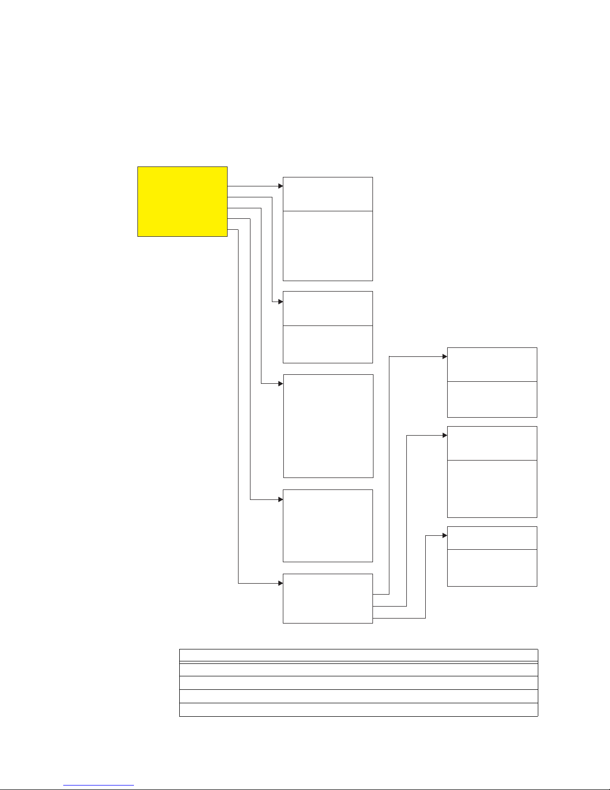
ETHERNET INTERFACE CHAPTER 1: COMMUNICATIONS GUIDE
S1 DNP GENERAL
DNP ADDRESS
DNP TCP/UDP PORT
CHANNEL 1 PORT
CHANNEL 2 PORT
TME SYNC IIN PER.
DNP MSG FRAG SIZE
DNP TCP CONN. T/O
▼
S1 DNP
DNP GENERAL
DNP UNSOL RESPONSE*
DEFAULT VARIATION
DNP CLIENT ADDRESS*
DNP POINTS LIST
897769.cdr
DNP CLIENT ADDRESS*
CLIENT ADDRESS 1
CLIENT ADDRESS 2
CLIENT ADDRESS 3
CLIENT ADDRESS 4
CLIENT ADDRESS 5
POINT 0
...
POINT 1
POINT 2
POINT 63
▼
S1 DNP POINTS LIST
BINARY INPUTS
BINARY OUTPUT
ANALOG INPUTS
POINT 0 ENTRY
...
POINT 1 ENTRY
POINT 31 ENTRY
▼
POINT 0 ON
...
POINT 0 OFF
POINT 1 ON
POINT 1 OFF
POINT 15 ON
POINT 15 OFF
▼
DEFAULT VARIATION
DNP OBJECT 1
DNP OBJECT 2
DNP OBJECT 20
DNP OBJECT 21
DNP OBJECT 22
DNP OBJECT 23
DNP OBJECT 30
DNP OBJECT 32
DNP UNSOL RESPONSE*
FUNCTION
▼
TIMEOUT
MAX RETRIES
DEST ADDRESS
* Ethernet only
DNP Ethernet protocol settings
DNP communication The menu structure for the DNP protocol is shown below.
The following path is available using the keypad. For instructions on how to use the
keypad, please refer to Chapter 3 - Working with the Keypad.
PATH:
SETPOINTS > RELAY SETUP > COMMUNICATIONS > DNP PROTOCOL > DNP GENERAL
DNP device profile
1–38 345 TRANSFORMER PROTECTION SYSTEM – COMMUNICATIONS GUIDE
DNP 3.0 Device Profile
(Also see the IMPLEMENTATION TABLE in the following section)
Vendor Name: General Electric Multilin
Device Name: SR345 Relay
Page 43

CHAPTER 1: COMMUNICATIONS GUIDE ETHERNET INTERFACE
DNP 3.0 Device Profile
Highest DNP Level Supported:
For Requests: Level 2
For Responses: Level 2
Device Function:
□ Master
⊠ Slave
Notable objects, functions, and/or qualifiers supported in addition to the Highest DNP Levels
Supported (the complete list is described in the attached table):
Binary Inputs (Object 1)
Binary Input Changes (Object 2)
Binary Outputs (Object 10)
Control Relay Output Block (Object 12)
Binary Counters (Object 20)
Frozen Counters (Object 21)
Counter Change Event (Object 22)
Frozen Counter Event (Object 23)
Analog Inputs (Object 30)
Analog Input Changes (Object 32)
Analog Deadbands (Object 34)
Time and Date (Object 50)
Internal Indications (Object 80)
Maximum Data Link Frame Size (octets): Maximum Application Fragment Size (octets):
Transmitted: 292 Transmitted: configurable up to 2048
Received: 292 Received: 2048
Maximum Data Link Re-tries: Maximum Application Layer Re-tries:
⊠None ⊠ None
□Fixed at 3 □ Configurable
□Configurable
Requires Data Link Layer Confirmation:
⊠ Never
□ Always
□ Sometimes
□ Configurable
Requires Application Layer Confirmation:
□ Never
□ Always
⊠ When reporting Event Data
⊠ When sending multi-fragment responses
□ Sometimes
□ Configurable
345 TRANSFORMER PROTECTION SYSTEM – COMMUNICATIONS GUIDE 1–39
Page 44

ETHERNET INTERFACE CHAPTER 1: COMMUNICATIONS GUIDE
DNP 3.0 Device Profile
Timeouts while waiting for:
Data Link Confirm: ⊠ None □ Fixed □ Variable □ Configurable
Complete Appl. Fragment: ⊠ None □ Fixed □ Variable □ Conf igurable
Application Confirm: □ None ⊠ Fixed at 10 s □ Variable □ Conf igurable
Complete Appl. Response: ⊠ None □ Fixed at ___ □ Variable □ Configurable
Others:
Transmission Delay: No intentional delay
Need Time Interval: Configurable (default = 24 hrs.)
Select/Operate Arm Timeout: 10 s
Binary input change scanning period: 8 times per power system cycle
Analog input change scanning period: 500 ms
Counter change scanning period: 500 ms
Frozen counter event scanning period: 500 ms
Sends/Executes Control Operations:
WRITE Binary Outputs ⊠ Never □ Always □ Sometimes □Conf igurable
SELECT/OPERATE □ Never ⊠ Always □ Sometimes □ Configurable
DIRECT OPERATE □ Never ⊠Always
□ Sometimes □ Configurable
DIRECT OPERATE – NO ACK □ Never ⊠ Always □ Sometimes □ Configurable
Count > 1 ⊠ Never □ Always □ Sometimes □ Configurable
Pulse On □ Never □ Always ⊠ Sometimes □ Configurable
Pulse Off □ Never □ Always ⊠ Sometimes □ Configurable
Latch On □ Never □ Always ⊠ Sometimes □ Configurable
Latch Off □ Never □ Always ⊠ Sometimes □ Configurable
Queue ⊠ Never □ Always □ Sometimes □ Configurable
Clear Queue ⊠ Never □ Always □ Sometimes □ Configurable
Explanation of ‘Sometimes’: Object 12 points are mapped to Virtual Inputs. Both “Pulse On” and
“Latch On” operations perform the same function in the 345; that is, the appropriate Virtual Input is
put into the “On” state. The On/Off times and Count value are ignored. “Pulse Off” and “Latch Off”
operations put the appropriate Virtual Input into the “Off” state.
Reports Binary Input Change Events when no
specific variation requested:
Reports time-tagged Binary Input Change
Events when no specific variation
requested:
□ Never □ Never
⊠ Only time-tagged ⊠ Binary Input Change With Time
□ Only non-time-tagged □ Binary Input Change With Relative Time
□ Configurable □ Configurable (attach explanation)
Sends Unsolicited Responses: Sends Static Data in Unsolicited Responses:
□ Never ⊠ Never
□ Configurable □ When Device Restarts
□ Only certain objects □ When Status Flags Change
⊠ Sometimes No other options are permitted.
⊠ ENABLE/DISABLE unsolicited Function codes
supported
Explanation of ‘Sometimes’: It will be disabled for
RS-485 applications, since there is no collision
avoidance mechanism. For Ethernet communication
it will be available and it can be disabled or enabled
with the proper function code.
1–40 345 TRANSFORMER PROTECTION SYSTEM – COMMUNICATIONS GUIDE
Page 45

CHAPTER 1: COMMUNICATIONS GUIDE ETHERNET INTERFACE
DNP 3.0 Device Profile
Default Counter Object/Variation: Counters Roll Over at:
□ No Counters Reported □ No Counters Reported
□ Configurable (attach explanation) □ Configurable (attach explanation)
⊠ Default Object: 20 ⊠ 16 Bits
Default Variation: 1
⊠ Point-by-point list attached □ Other Value: _____
⊠ Point-by-point list attached
Sends Multi-Fragment Responses:
⊠ Yes
□ No
DNP port allocation
Channel 1 Port Channel 2 Port DNP Availability
None None DNP not available over Ethernet port
None NETWORK-TCP One Master over TCP
None NETWORK-UDP "Various" Masters over UDP
NETWORK-TCP None One Master over TCP
NETWORK-TCP NETWORK-TCP Two Masters over TCP
NETWORK-TCP NETWORK-UDP One Master over TCP and "various" Masters over UDP
NETWORK-UDP None "Various" Masters over UDP
NETWORK-UDP NETWORK-TCP "Various" Masters over UDP and one Master over TCP
NETWORK-UDP NETWORK-UDP "Various" Masters over UDP
The DNP Eth Channel 1 Port and DNP Eth Channel 2 Port settings select the
communications port assigned to the DNP protocol for each Ethernet channel. When this
setting is set to "Network-TCP" the DNP protocol can be used over TCP/IP channels 1 or 2.
When this value is set to "Network-UDP" the DNP protocol can be used over UDP/IP on one
channel only.
345 TRANSFORMER PROTECTION SYSTEM – COMMUNICATIONS GUIDE 1–41
Page 46

ETHERNET INTERFACE CHAPTER 1: COMMUNICATIONS GUIDE
DNP implementation Table 16: DNP Implementation
OBJECT REQUEST RESPONSE
OBJECT
NO.
1 0 Binary Input (Variation 0
2 0 Binary Input Change
10 0 Binary Output Status
12 1 Control Relay Output
20 0 Binary Counter
VARIATION
NO.
1 Binary Input 1 (read) 22
2 Binary Input with Status 1 (read) 22
1 Binary Input Change
2 Binary Input Change
3 Binary Input Change
2 Binary Output Status 1 (read) 00, 01 (start-stop)
DESCRIPTION FUNCTION
is used to request
default variation)
(Variation 0 is used to
request default
variation)
without Time
with Time
with Relative Time
(Variation 0 is used to
request default
variation)
Block
(Variation 0 is used to
request default
variation)
CODES
(DEC)
1 (read) 22
(assign
class)
(assign
class)
(assign
class)
1 (read) 06 (no range, or all)
1 (read) 06 (no range, or all)
1 (read) 06 (no range, or all)
1 (read) 06 (no range, or all)
1 (read) 00, 01(start-stop)
3 (select)4
(operate) 5
(direct op) 6
(dir. op,
noack)
1 (read) 7
(freeze) 8
(freeze
noack) 9
(freeze clear)
10 (frz. cl.
noack) 22
(assign
class)
QUALIFIER CODES
(HEX)
00, 01 (start-stop)
06 (no range, or all)
07, 08 (limited
quantity) 17, 28
(index)
00, 01 (start-stop)
06 (no range, or all)
07, 08 (limited
quantity) 17, 28
(index)
00, 01 (start-stop)
06 (no range, or all)
07, 08 (limited
quantity) 17, 28
(index)
07, 08 (limited
quantity)
07, 08 (limited
quantity)
07, 08 (limited
quantity)
07, 08 (limited
quantity)
06 (no range, or all)
07, 08 (limited
quantity) 17, 28
(index)
06 (no range, or all)
07, 08 (limited
quantity) 17, 28
(index)
00, 01 (start-stop)
07, 08 (limited
quantity) 17, 28
(index)
00, 01 (start-stop)
06 (no range, or all)
07, 08 (limited
quantity) 17, 28
(index)
FUNCTION
CODES
(DEC)
--- ---
129
(response)
129
(response)
--- ---
129
(response)
130 (unsol.
resp.)
129
(response)
130 (unsol.
resp.)
--- ---
--- ---
129
(response)
129
(response)
--- ---
QUALIFIER
CODES
(HEX)
00, 01
(start-stop)
17, 28
(index) (see
Note 2)
00, 01
(start-stop)
17, 28
(index) (see
Note 2)
17, 28
(index)
17, 28
(index)
00, 01
(start-stop)
17, 28
(index) (see
Note 2)
echo of
request
1–42 345 TRANSFORMER PROTECTION SYSTEM – COMMUNICATIONS GUIDE
Page 47

CHAPTER 1: COMMUNICATIONS GUIDE ETHERNET INTERFACE
OBJECT REQUEST RESPONSE
OBJECT
NO.
VARIATION
NO.
DESCRIPTION FUNCTION
CODES
(DEC)
1 32-Bit Binary Counter 1 (read)7
(freeze) 8
(freeze
noack) 9
(freeze clear)
QUALIFIER CODES
(HEX)
00, 01 (start-stop)
06 (no range, or all)
07, 08 (limited
quantity) 17, 28
(index)
FUNCTION
CODES
(DEC)
129
(response)
QUALIFIER
CODES
(HEX)
00, 01
(start-stop)
17, 28
(index) (see
Note 2)
10 (frz. cl.
noack) 22
(assign
class)
2 16-Bit Binary Counter 1 (read) 7
(freeze) 8
(freeze
noack) 9
(freeze clear)
00, 01 (start-stop)
06 (no range, or all)
07, 08 (limited
quantity) 17, 28
(index)
129
(response)
00, 01
(start-stop)
17, 28
(index) (see
Note 2)
10 (frz. cl.
noack) 22
(assign
class)
5 32-Bit Binary Counter
without Flag
1 (read) 7
(freeze) 8
(freeze
noack) 9
(freeze clear)
00, 01 (start-stop)
06 (no range, or all)
07, 08 (limited
quantity) 17, 28
(index)
129
(response)
00, 01
(start-stop)
17, 28
(index) (see
Note 2)
10 (frz. cl.
noack) 22
(assign
class)
6 16-Bit Binary Counter
without Flag
1 (read) 7
(freeze) 8
(freeze
noack) 9
(freeze clear)
00, 01 (start-stop)
06 (no range, or all)
07, 08 (limited
quantity) 17, 28
(index)
129
(response)
00, 01
(start-stop)
17, 28
(index) (see
Note 2)
10 (frz. cl.
noack) 22
(assign
class)
21 0 Frozen
Counter(Variation 0 is
used to request
defaultvariation)
1 (read) 22
(assign
class)
00, 01 (start-stop)
06 (no range, or all)
07, 08 (limited
quantity) 17, 28
--- ---
(index)
1 32-Bit Frozen Counter 1 (read) 22
2 16-Bit Frozen Counter 1 (read) 22
9 32-Bit Frozen Counter
without Flag
10 16-Bit Frozen Counter
without Flag
22 0 Counter Change Event
(Variation 0 is used to
request default
(assign
class)
(assign
class)
1 (read) 22
(assign
class)
1 (read) 22
(assign
class)
1 (read) 06 (no range, or all)
00, 01 (start-stop)
06 (no range, or all)
07, 08 (limited
quantity) 17, 28
(index)
00, 01 (start-stop)
06 (no range, or all)
07, 08 (limited
quantity) 17, 28
(index)
00, 01 (start-stop)
06 (no range, or all)
07, 08 (limited
quantity) 17, 28
(index)
00, 01 (start-stop)
06 (no range, or all)
07, 08 (limited
quantity) 17, 28
(index)
07, 08 (limited
quantity)
129
(response)
00, 01
(start-stop)
17, 28
(index) (see
Note 2)
129
(response)
00, 01
(start-stop)
17, 28
(index) (see
Note 2)
129
(response)
00, 01
(start-stop)
17, 28
(index) (see
Note 2)
129
(response)
00, 01
(start-stop)
17, 28
(index) (see
Note 2)
--- ---
variation)
345 TRANSFORMER PROTECTION SYSTEM – COMMUNICATIONS GUIDE 1–43
Page 48

ETHERNET INTERFACE CHAPTER 1: COMMUNICATIONS GUIDE
OBJECT REQUEST RESPONSE
OBJECT
NO.
VARIATION
DESCRIPTION FUNCTION
NO.
1 32-Bit Counter Change
Event
CODES
(HEX)
(DEC)
1 (read) 06 (no range, or all)
07, 08 (limited
quantity)
QUALIFIER CODES
FUNCTION
CODES
(DEC)
129
(response)
130 (unsol.
QUALIFIER
CODES
(HEX)
17, 28
(index)
resp.)
23 2 16-Bit Counter Change
Event
1 (read) 06 (no range, or all)
07, 08 (limited
quantity)
129
(response)
130 (unsol.
17, 28
(index)
resp.)
5 32-Bit Counter Change
Event with Time
1 (read) 06 (no range, or all)
07, 08 (limited
quantity)
129
(response)
130 (unsol.
17, 28
(index)
resp.)
6 16-Bit Counter Change
Event with Time
1 (read) 06 (no range, or all)
07, 08 (limited
quantity)
129
(response)
130 (unsol.
17, 28
(index)
resp.)
0 Frozen Counter Event
(Variation 0 is used to
request default
1 (read) 06 (no range, or all)
07, 08 (limited
quantity)
--- ---
variation)
1 32-Bit Frozen Counter
Event
1 (read) 06 (no range, or all)
07, 08 (limited
quantity)
129
(response)
130 (unsol.
17, 28
(index)
resp.)
2 16-Bit Frozen Counter
Event
1 (read) 06 (no range, or all)
07, 08 (limited
quantity)
129
(response)
130 (unsol.
17, 28
(index)
resp.)
5 32-Bit Frozen Counter
Event with Time
1 (read) 06 (no range, or all)
07, 08 (limited
quantity)
129
(response)
130 (unsol.
17, 28
(index)
resp.)
6 16-Bit Frozen Counter
Event with Time
1 (read) 06 (no range, or all)
07, 08 (limited
quantity)
129
(response)
130 (unsol.
17, 28
(index)
resp.)
30 0 Analog Input (Variation
0 is used to request
default variation)
1 (read) 22
(assign
class)
00, 01 (start-stop)
06 (no range, or all)
07, 08 (limited
--- ---
quantity) 17, 28
(index)
1 32-Bit Analog Input 1 (read) 22
(assign
class)
2 16-Bit Analog Input 1 (read) 22
(assign
class)
3 32-Bit Analog Input
without Flag
1 (read) 22
(assign
class)
4 16-Bit Analog Input
without Flag
1 (read) 22
(assign
class)
00, 01 (start-stop)
06 (no range, or all)
07, 08 (limited
quantity) 17, 28
(index)
00, 01 (start-stop)
06 (no range, or all)
07, 08 (limited
quantity) 17, 28
(index)
00, 01 (start-stop)
06 (no range, or all)
07, 08 (limited
quantity) 17, 28
(index)
00, 01 (start-stop)
06 (no range, or all)
07, 08 (limited
quantity) 17, 28
(index)
129
(response)
129
(response)
129
(response)
129
(response)
00, 01
(start-stop)
17, 28
(index) (see
Note 2)
00, 01
(start-stop)
17, 28
(index) (see
Note 2)
00, 01
(start-stop)
17, 28
(index) (see
Note 2)
00, 01
(start-stop)
17, 28
(index) (see
Note 2)
1–44 345 TRANSFORMER PROTECTION SYSTEM – COMMUNICATIONS GUIDE
Page 49

CHAPTER 1: COMMUNICATIONS GUIDE ETHERNET INTERFACE
OBJECT REQUEST RESPONSE
OBJECT
NO.
32 0 Analog Change Event
VARIATION
NO.
DESCRIPTION FUNCTION
CODES
(DEC)
1 (read) 06 (no range, or all)
(Variation 0 is used to
request default
QUALIFIER CODES
(HEX)
07, 08 (limited
quantity)
FUNCTION
CODES
(DEC)
QUALIFIER
CODES
(HEX)
--- ---
variation)
1 32-Bit Analog Change
Event without Time
1 (read) 06 (no range, or all)
07, 08 (limited
quantity)
129
(response)
130 (unsol.
17, 28
(index)
resp.)
2 16-Bit Analog Change
Event without Time
1 (read) 06 (no range, or all)
07, 08 (limited
quantity)
129
(response)
130 (unsol.
17, 28
(index)
resp.)
3 32-Bit Analog Change
Event with Time
1 (read) 06 (no range, or all)
07, 08 (limited
quantity)
129
(response)
130 (unsol.
17, 28
(index)
resp.)
4 16-Bit Analog Change
Event with Time
1 (read) 06 (no range, or all)
07, 08 (limited
quantity)
129
(response)
130 (unsol.
17, 28
(index)
resp.)
34 0 Analog Input Reporting
Deadband (Variation 0 is
used to request
defaultvariation)
1 (read) 00, 01 (start-stop)
06 (no range, or all)
07, 08 (limited
quantity) 17, 28
--- ---
(index)
1 16-bit Analog Input
Reporting Deadband
(default - see Note 1)
1 (read) 00, 01 (start-stop)
06 (no range, or all)
07, 08 (limited
quantity) 17, 28
(index)
2 (write) 00, 01 (start-stop)
129
(response)
00, 01
(start-stop)
17, 28
(index) (see
Note 2)
--- --07, 08 (limited
quantity) 17, 28
(index)
2 32-bit Analog Input
Reporting Deadband
1 (read) 00, 01 (start-stop)
06 (no range, or all)
07, 08 (limited
quantity) 17, 28
(index)
2 (write) 00, 01 (start-stop)
129
(response)
00, 01
(start-stop)
17, 28
(index) (see
Note 2)
--- --07, 08 (limited
quantity) 17, 28
(index)
50 1 T ime and Date (default -
see Note 1)
52 2 T ime Delay Fine
(quantity = 1)
60 0 Class 0, 1, 2, and 3 Data 1 (read) 20
1 (read)2
(write)
129
(response)
00, 01 (start-stop)
06 (no range, or all)
07 (limited qty=1) 08
(limited quantity)
17, 28 (index)
129
(response)
00, 01
(start-stop)
17, 28
(index) (see
Note 2)
07 (limited quantity) --- ---
06 (no range, or all) --- ---
(enable
unsol) 21
(disable
unsol) 22
(assign
class)
1 Class 0 Data 1 (read) 22
06 (no range, or all) --- ---
(assign
class)
345 TRANSFORMER PROTECTION SYSTEM – COMMUNICATIONS GUIDE 1–45
Page 50

ETHERNET INTERFACE CHAPTER 1: COMMUNICATIONS GUIDE
NOTE
OBJECT REQUEST RESPONSE
OBJECT
NO.
VARIATION
NO.
DESCRIPTION FUNCTION
CODES
(DEC)
2 Class 1 Data 1 (read) 20
(enable
unsol)
3 Class 2 Data 21 (disable
QUALIFIER CODES
(HEX)
06 (no range, or all)
07, 08 (limited
quantity)
FUNCTION
CODES
(DEC)
QUALIFIER
CODES
(HEX)
--- ---
--- ---
unsol)
4 Class 3 Data 22 (assign
--- ---
class)
80 1 Internal Indications 1 (read) 00, 01 (start-stop)
(index =7)
2 (write) (see
Note 3)
No Object (function
code only) see Note 3
No Object (function
code only)
No Object (function
code only)
NOTE:
1. A default variation refers to the variation response when variation 0 is requested and/
13 (cold
restart)
14 (warm
restart)
23 (delay
meas.)
00 (start-stop)
(index =7)
--- --- ---
--- --- ---
--- --- ---
129
(response)
00, 01
(start-stop)
--- ---
or in class 0, 1, 2, or 3 scans. The default variations for object types 1, 2, 20, 21, 22, 23,
30, and 32 are selected via relay settings. This optimizes the class 0 poll data size.
2. For static (non-change-event) objects, qualifiers 17 or 28 are only responded when a
request is sent with qualifiers 17 or 28, respectively. Otherwise, static object requests
sent with qualifiers 00, 01, 06, 07, or 08, will be responded with qualifiers 00 or 01 (for
changeevent objects, qualifiers 17 or 28 are always responded.)
3. Cold restarts are implemented the same as warm restarts – the 345 is not restarted,
but the DNP process is restarted.
1–46 345 TRANSFORMER PROTECTION SYSTEM – COMMUNICATIONS GUIDE
Page 51

CHAPTER 1: COMMUNICATIONS GUIDE ETHERNET INTERFACE
DNP Ethernet
EnerVista Setup
NOTE:
Table 17: DNP protocol
SETTINGS PARAMETER RANGE FORMAT
DNP Channel 1 Port NONE NONE ; COM-RS485 ; NETWORK-
TCP ; NETWORK –UDP
DNP Channel 2 Port NONE NONE ; COM-RS485 ; NETWORK-
TCP ; NETWORK –UDP
DNP Address 65519 0 to 65519 F1
DNP Client Address 1 0. 0. 0. 0 F150
DNP Client Address 2 0. 0. 0. 0 F150
DNP Client Address 3 0. 0. 0. 0 F150
DNP Client Address 4 0. 0. 0. 0 F150
DNP Client Address 5 0. 0. 0. 0 F150
DNP TCP/UDP Port Number 20000 0 to 65535 F1
DNP Unsol Resp Function Disabled Disabled ; Enabled F126
DNP Unsol Resp Timeout 5 s 0 to 60 s F1
DNP Unsol Resp Max Retries 10 1 to 255 F1
DNP Unsol Resp Dest Addr 1 0 to 65519 F1
DNP Time Sync IIN Period 1440 min 1 to 10080 min F1
DNP Message Fragment Size 240 30 to 2048 F1
DNP Object 1 Default Variation 2 1 ; 2 F1
DNP Object 2 Default Variation 2 1 ; 2 F1
DNP Object 20 Default Variation 1 1 ; 2 , 5 ; 6 F78
DNP Object 21 Default Variation 1 1 ; 2 ; 9 ; 10 F79
DNP Object 22 Default Variation 1 1 ; 2 , 5 ; 6 F80
DNP Object 23 Default Variation 1 1 ; 2 , 5 ; 6 F81
DNP Object 30 Default Variation 1 1 ; 2 ;3 ; 4 F82
DNP Object 32 Default Variation 1 1 ; 2 ;3 ; 4 F83
DNP TCP Connection Timeout 120 s 10 to 300 s F1
F87
F87
The setting DNP Unsolicited Response Timeout affects DNP TCP clients only; not serial
and UDP clients. Possible values that can be selected for this setting lie between 0 and 60
seconds.
In addition to this selected timeout, up to an additional 10 seconds is required to send
the response packet.
345 TRANSFORMER PROTECTION SYSTEM – COMMUNICATIONS GUIDE 1–47
Page 52

ETHERNET INTERFACE CHAPTER 1: COMMUNICATIONS GUIDE
NOTE
Table 18: DNP point list
SETTINGS PARAMETER RANGE FORMAT
Binary Input Point 0 Entry Select entry
from a list
Operands F134
Binary Input Point 63 Entry Select entry
Analog Input Point 0 Entry Select entry
Analog Input Point 0 Scale Factor 1 0.001 ; 0.01 ; 0.1 ; 1 ; 10 ; 100 ;
Analog Input Point 0 Deadband 30000 0 to 100000000 F9
Analog Input Point 31 Entry Select entry
Analog Input Point 31 Scale
Factor
Analog Input Point 31 Deadband 30000 0 to 100000000 F9
Binary Output Point 0 ON Select entry
Binary Output Point 0 OFF Select entry
Binary Output Point 15 ON Select entry
Binary Output Point 15 OFF Select entry
from a list
from a list
from a list
1 0.001 ; 0.01 ; 0.1 ; 1 ; 10 ; 100 ;
from a list
from a list
from a list
from a list
Operands F134
Analog parameters
1000 ; 10000 ; 100000
Analog parameters
1000 ; 10000 ; 100000
Virtual Input 1 to 32 and Force
Coils
Virtual Input 1 to 32 and Force
Coils
Virtual Input 1 to 32 and Force
Coils
Virtual Input 1 to 32 and Force
Coils
F85
F85
F86
F86
F86
F86
• The DNP Time Sync IIN Period setting determines how often the Need Time Internal
Indication (IIN) bit is set by the 345. Changing this time allows the 345 to indicate that
a time synchroniztion command is necessary more or less often
• Various settings have been included to configure Default Variation for the Binary
Inputs, Counters and Analog Inputs Objects. The default variation refers to the
variation response when variation 0 is requested, and/or in class 0, 1, 2, or 3 scans
• Up to 64 Binary Inputs and 32 Analog Input entries can be mapped to an item from a
list of 345 status events and metered values. Status events correspond to Funcion
Code 134B.
• Each Analog Input point Deadband and Scale Factor can be set individually instead of
setting a general deadband or scale for different metering groups. This will avoid scale
and deadband conflicts for different meterings of the same nature.
• Up to 16 Binary/Control Outputs can be configured by selecting a Virtual Input or
Command from a list of 32 Virtual Inputs and Commands (Force Coils). Some legacy
DNP implementations use a mapping of one DNP Binary Output to two physical or
virtual control points. In Order to configure Paired Control Points the source for states
ON and OFF should be set to different Virtual Inputs or Commands.
• The DNP Technical Committee recommends using contiguous point numbers, starting
at 0, for each data type, because some DNP3 Master implementations allocate
contiguous memory from point 0 to the last number for each data type.
NOTE:
Binary Inputs are inputs to the Master. Binary Outputs are outputs from the Master.
1–48 345 TRANSFORMER PROTECTION SYSTEM – COMMUNICATIONS GUIDE
Page 53

CHAPTER 1: COMMUNICATIONS GUIDE ETHERNET INTERFACE
DNP general Default variations for Object 1, 2 , 20 , 21 , 22 , 23 , 30 and Object 32 will be set by settings
and returned for the object in a response when no specific variation is specified in a Master
request.
Any change in the state of any binary point causes the generation of an event, and
consequently, if configured, an unsolicited response, or it is returned when the Master asks
for it. The same behaviour will be seen when an analog value changes by more than its
configured deadband limit . There can be up to 3 Masters in total, but only one Serial
Master.
The following Default Classes will be fixed for the different blocks of data:
Binary Input Points Default Class = 1
Analog Input Point Default Class = 2
Counters Default Class = 3
Each Data Point Class can be changed by protocol function code 22 in volatile mode. If a
restart is performed, the new values will be lost.
DNP Object 34 points can be used to change deadband values from the default for each
individual DNP Analog Input point. These new deadbands will be maintained such that in
the case of a relay restart, the values are not lost.
Requests for Object 20 (Binary Counters), Object 21 (Frozen Counters), and Object 22
(Counter Change Events) must be accepted.
Function codes “Immediate Freeze”, “Freeze and Clear” etc. are accepted as well.
345 TRANSFORMER PROTECTION SYSTEM – COMMUNICATIONS GUIDE 1–49
Page 54
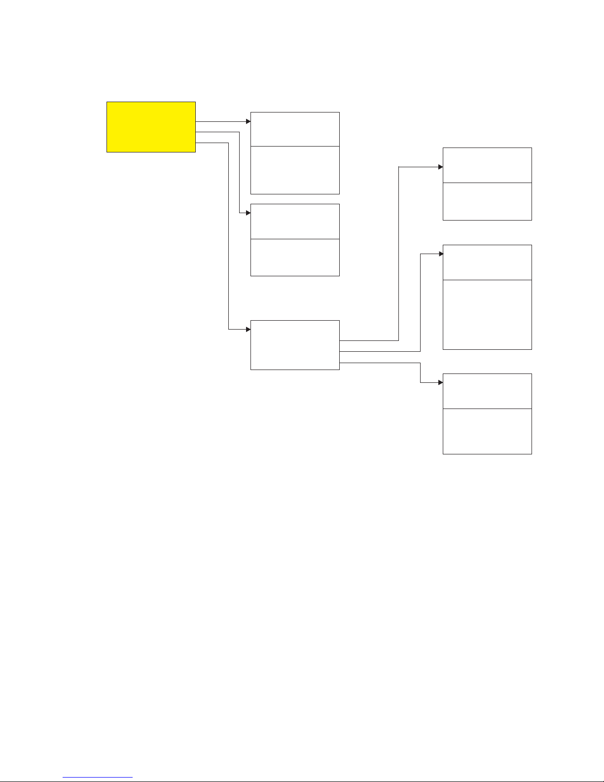
ETHERNET INTERFACE CHAPTER 1: COMMUNICATIONS GUIDE
104 BINARY INPUTS
POINT 0
POINT 1
...
POINT 63
▼
S1 104 GENERAL
FUNCTION
CYCLIC DATA PERIOD
TCP CONN. TIMEOUT
TCP PORT
SLAVE ADDRESS
▼
897794.cdr
S1 104 POINT LIST
BINARY INPUTS
ANALOG INPUTS
BINARY OUTPUTS
S1 60870-5-104
GENERAL
CLIENT ADDRESS
POINT LIST
104 ANALOG INPUTS
POINT 0 ENTRY
POINT 0 SCALE FCTR
POINT 0 DEADBAND
...
POINT 31 ENTRY
POINT 31 SCALE FCTR
POINT 31 DEADBAND
▼
S1 104 CLIENT ADDRESS
CLIENT ADDRESS 1
CLIENT ADDRESS 2
...
CLIENT ADDRESS 5
▼
.
.
.
.
104 BINARY OUTPUTS
POINT 0 ON:
POINT 0 OFF:
...
POINT 15 ON:
POINT 15 OFF:
▼
.
.
.
.
IEC60870-5-104 protocol
IEC 60870-5-104
interoperability
This document is adapted from the IEC 60870-5-104 standard. For this section the boxes
indicate the following: ⊠ – used in the standard direction; □– not used.
IEC 60870-5-104 Interoperability Document
1. System or device:
□ System definition.
□ Controlling station definition (master).
⊠ Controlled station definition (slave).
2. Application layer:
3. Transmission mode for application data:
Mode 1 (least significant octet first), as defined in Clause 4.10 of IEC 60870-5-4, is used
exclusively in this companion standard.
4. Common address of ADSU:
⊠ Two octets.
5. Information object address:
⊠ Three octets.
⊠ Structured
⊠ Unstructured
6. Cause of transmission:
1–50 345 TRANSFORMER PROTECTION SYSTEM – COMMUNICATIONS GUIDE
Page 55

CHAPTER 1: COMMUNICATIONS GUIDE ETHERNET INTERFACE
⊠ Two octets (with originator address). Originator address is set to zero if not used.
7. Maximum length of APDU.
253 in both directions (the maximum length is a fixed system parameter).
8. Selection of standard ASDUs.
For the following lists, the boxes indicate the following: ⊠ – used in standard direction;
□ – not used.
Process information in monitor direction:
Table 19: Process information in monitor direction
Number / description Mnemonic
⊠ <1> := Single-point information M_SP_NA_1
□ <3> := Double-point information M_DP_NA_1
□ <5> := Step position information M_ST_NA_1
□ <7> := Bitstring of 32 bits M_BO_NA_1
□ <9> := Measured value, normalized value M_ME_NA_1
⊠ <11> := Measured value, scaled value M_ME_NB_1
□ <13> := Measured value, short floating point value M_ME_NC_1
⊠ <15> := Integrated totals M_IT_NA_1
□ <20> := Packed single-point information with status change detection M_SP_NA_1
□ <21> := Measured value, normalized value without quantity descriptor M_ME_ND_1
⊠ <30> := Single-point information with time tag CP56Time2a M_SP_TB_1
□ <31> := Double-point information with time tag CP56Time2a M_DP_TB_1
□ <32> := Step position information with time tag CP56Time2a M_ST_TB_1
□ <33> := Bitstring of 32 bits with time tag CP56Time2a M_BO_TB_1
□ <34> := Measured value, normalized value with time tag CP56Time2a M_ME_TD_1
⊠ <35> := Measured value, scaled value with time tag CP56Time2a M_ME_TE_1
□ <36> := Measured value, short floating point value with time tag CP56Time2a M_ME_TF_1
⊠ <37> := Integrated totals with time tag CP56Time2a M_IT_TB_1
□ <38> := Event of protection equipment with time tag CP56Time2a M_EP_TD_1
□ <39> := Packed start events of protection equipment with time tag
CP56Time2a
□ <40> := Packed output circuit information of protection equipment with time
tag CP56Time2a
M_EP_TE_1
M_EP_TF_1
345 TRANSFORMER PROTECTION SYSTEM – COMMUNICATIONS GUIDE 1–51
Either the ASDUs of the set <2>, <4>, <6>, <8>, <10>, <12>, <14>, <16>, <17>, <18>,
and <19> or of the set <30> to <40> are used.
Page 56

ETHERNET INTERFACE CHAPTER 1: COMMUNICATIONS GUIDE
Table 20: Process information in control direction
Number / description Mnemonic
⊠ <45> := Single command C_SC_NA_1
⊠ <46> := Double command C_DC_NA_1
□ <47> := Regulating step command C_RC_NA_1
□ <48> := Set point command, normalized value C_SE_NA_1
□ <49> := Set point command, scaled value C_SE_NB_1
□ <50> := Set point command, short floating point value C_SE_NC_1
□ <51> := Bitstring of 32 bits C_BO_NA_1
⊠ <58> := Single command with time tag CP56Time2a C_SC_TA_1
⊠ <59> := Double command with time tag CP56Time2a C_DC_TA_1
□ <60> := Regulating step command with time tag CP56Time2a C_RC_TA_1
□ <61> := Set point command, normalized value with time tag CP56Time2a C_SE_TA_1
□ <62> := Set point command, scaled value with time tag CP56Time2a C_SE_TB_1
□ <63> := Set point command, short floating point value with time tag
CP56Time2a
□ <64> := Bitstring of 32 bits with time tag CP56Time2a C_BO_TA_1
C_SE_TC_1
Either the ASDUs of the set <45> to <51> or of the set <58> to <64> are used.
Table 21: System information in monitor direction
Number / description Mnemonic
⊠ <70> := End of initialization M_EI_NA_1
Table 22: System information in control direction
Number / description Mnemonic
⊠ <100> := Interrogation command C_IC_NA_1
⊠ <101> := Counter interrogation command C_CI_NA_1
⊠ <102> := Read command C_RD_NA_1
⊠ <103> := Clock synchronization command (see Clause 7.6 in standard) C_CS_NA_1
⊠ <105> := Reset process command C_RP_NA_1
⊠ <107> := Test command with time tag CP56Time2a C_TS_TA_1
Table 23: Parameter in control direction
Number / description Mnemonic
□ <110> := Parameter of measured value, normalized value PE_ME_NA_1
⊠ <111> := Parameter of measured value, scaled value PE_ME_NB_1
□ <112> := Parameter of measured value, short floating point value PE_ME_NC_1
□ <113> := Parameter activation PE_AC_NA_1
Table 24: File transfer
Number / description Mnemonic
□ <120> := File ready F_FR_NA_1
□ <121> := Section ready F_SR_NA_1
□ <122> := Call directory, select file, call file, call section F_SC_NA_1
□ <123> := Last section, last segment F_LS_NA_1
□ <124> := Ack file, ack section F_AF_NA_1
□ <125> := Segment F_SG_NA_1
□ <126> := Directory (blank or X, available only in monitor [standard] direction) F_DR_TA_1
□ <127> := Query log - Request archive file F_SC_NB_1
1–52 345 TRANSFORMER PROTECTION SYSTEM – COMMUNICATIONS GUIDE
Page 57

CHAPTER 1: COMMUNICATIONS GUIDE ETHERNET INTERFACE
Type identifier and cause of transmission assignments (station-specific parameters)
are shown in the following tables. In these tables, shaded boxes (░) are not required,
black boxes (█) are not permitted in the companion standard, empty cells indicate the
functions or ASDU are not used, and a cross (╳) indicates availability only in the
standard direction.
Table 25: Cause of transmission numbers
Number Cause of transmission
1 Periodic, cyclic
2 Background scan
3 Spontaneous
4 Initialized
5 Request or requested
6 Activation
7 Activation confirmation
8 Deactivation
9 Deactivation confirmation
10 Activation termination
11 Return information caused by local command
12 File transfer
13 Interrogated by group <number>
20 to 36 Requested by group <n> counter request
37 to 41 Unknown type identification
44 Unknown cause of transmission
45 Unknown command address of ADSU
46 Unknown information object address
47 Unknown information object address
Table 26: Cause of transmission assignments
Type identification Cause of transmission
No. Mnemonic 1 2 3 4 5 6 7 8 9 10 11 12 13
<1> M_SP_NA_1 ░ ╳░╳░░░░░╳╳░╳░░░░░
<2> M_SP_TA_1 ░░█░█░░░░░██░░░░░░░
<3> M_DP_NA_1 ░ ░ ░░░░░ ░ ░░░░░
<4> M_DP_TA_1 ░░█░█░░░░░██░░░░░░░
<5> M_ST_NA_1 ░ ░ ░░░░░ ░ ░░░░░
<6> M_ST_TA_1 ░░█░█░░░░░██░░░░░░░
<7> M_BO_NA_1 ░ ░ ░░░░░░░░ ░░░░░
<8> M_BO_TA_1 ░░█░█░░░░░░░░░░░░░░
<9> M_ME_NA_1 ░ ░░░░░░░░ ░░░░░
<10> M_ME_TA_1 ░░█░█░░░░░░░░░░░░░░
<11> M_ME_NB_1 ╳ ╳░╳░░░░░░░░╳░░░░░
<12> M_ME_TB_1 ░░█░█░░░░░░░░░░░░░░
<13> M_ME_NC_1 ░ ░░░░░░░░ ░░░░░
<14> M_ME_TC_1 ░░█░█░░░░░░░░░░░░░░
<15> M_IT_NA_1 ░░╳░░░░░░░░░░░╳░░░░
<16> M_IT_TA_1 ░░█░░░░░░░░░░░█░░░░
20
to
36
44 45 46
37
to
41
47
345 TRANSFORMER PROTECTION SYSTEM – COMMUNICATIONS GUIDE 1–53
Page 58

ETHERNET INTERFACE CHAPTER 1: COMMUNICATIONS GUIDE
Type identification Cause of transmission
No. Mnemonic 1 2 3 4 5 6 7 8 9 10 11 12 13
20
to
36
44 45 46
37
to
41
47
<17> M_EP_TA_1 ░░█░░░░░░░░░░░░░░░░
<18> M_EP_TB_1 ░░█░░░░░░░░░░░░░░░░
<19> M_EP_TC_1 ░░█░░░░░░░░░░░░░░░░
<20> M_PS_NA_1 ░ ░ ░░░░░░░░ ░░░░░
<21> M_ME_ND_1 ░ ░░░░░░░░ ░░░░░
<30> M_SP_TB_1 ░░╳░ ░░░░░╳╳░░░░░░░
<31> M_DP_TB_1 ░░ ░ ░░░░░ ░░░░░░░
<32> M_ST_TB_1 ░░ ░ ░░░░░ ░░░░░░░
<33> M_BO_TB_1 ░░ ░ ░░░░░░░░░░░░░░
<34> M_ME_TD_1 ░░ ░ ░░░░░░░░░░░░░░
<35> M_ME_TE_1 ░░ ░ ░░░░░░░░░░░░░░
<36> M_ME_TF_1 ░░ ░ ░░░░░░░░░░░░░░
<37> M_IT_TB_1 ░░╳░░░░░░░░░░░╳░░░░
<38> M_EP_TD_1 ░░ ░░░░░░░░░░░░░░░░
<39> M_EP_TE_1 ░░ ░░░░░░░░░░░░░░░░
<40> M_EP_TF_1 ░░ ░░░░░░░░░░░░░░░░
<45> C_SC_NA_1 ░░░░░╳╳╳╳╳░░░░░
<46> C_DC_NA_1 ░░░░░╳╳╳╳╳░░░░░
<47> C_RC_NA_1 ░░░░░ ░░░░░
<48> C_SE_NA_1 ░░░░░ ░░░░░
<49> C_SE_NB_1 ░░░░░ ░░░░░
<50> C_SE_NC_1 ░░░░░ ░░░░░
<51> C_BO_NA_1 ░░░░░ ░░░░░
<58> C_SC_TA_1 ░░░░░╳╳╳╳╳░░░░░
<59> C_DC_TA_1 ░░░░░╳╳╳╳╳░░░░░
<60> C_RC_TA_1 ░░░░░ ░░░░░
<61> C_SE_TA_1 ░░░░░ ░░░░░
<62> C_SE_TB_1 ░░░░░ ░░░░░
<63> C_SE_TC_1 ░░░░░ ░░░░░
<64> C_BO_TA_1 ░░░░░ ██ ░░░░░
<70> M_EI_NA_1*) ░░░╳░░░░░░░░░░░░░░░
<100> C_IC_NA_1 ░░░░░╳╳╳╳╳░░░░░
<101> C_CI_NA_1 ░░░░░╳╳░░╳░░░░░
<102> C_RD_NA_1 ░░░░╳░░░░░░░░░░
<103> C_CS_NA_1 ░░╳░░╳╳░░░░░░░░
<104> C_TS_NA_1 ░░░░░██░░░░░░░░████
<105> C_RP_NA_1 ░░░░░╳╳░░░░░░░░
<106> C_CD_NA_1 ░░█░░██░░░░░░░░████
<107> C_TS_TA_1 ░░░░░ ░░░░░░ ░
<110> P_ME_NA_1 ░░░░░ ░░░░░░ ░
<111> P_ME_NB_1 ░░░░░╳╳░░░░░░╳░
<112> P_ME_NC_1 ░░░░░ ░░░░░░ ░
<113> P_AC_NA_1 ░░░░░ ░░░░░░
<120> F_FR_NA_1 ░░░░░░░░░░░░ ░░
1–54 345 TRANSFORMER PROTECTION SYSTEM – COMMUNICATIONS GUIDE
Page 59

CHAPTER 1: COMMUNICATIONS GUIDE ETHERNET INTERFACE
Type identification Cause of transmission
No. Mnemonic 1 2 3 4 5 6 7 8 9 10 11 12 13
<121> F_SR_NA_1 ░░░░░░░░░░░░ ░░
<122> F_SC_NA_1 ░░░░ ░░░░░░░ ░░
<123> F_LS_NA_1 ░░░░░░░░░░░░ ░░
<124> F_AF_NA_1 ░░░░░░░░░░░░ ░░
<125> F_SG_NA_1 ░░░░░░░░░░░░ ░░
<126> F_DR_TA_1*) ░░ ░ ░░░░░░░░░░░░░░
<127> F_SC_NB_1*) ░░░░ ░░░░░░░ ░░
20
to
36
44 45 46
37
to
41
47
9. Basic application functions:
10. Station initialization:
⊠ Remote initialization.
11. Cyclic data transmission:
⊠ Cyclic data transmission.
12. Read procedure:
⊠ Read procedure.
13. Spontaneous transmission:
⊠ Spontaneous transmission.
14. Double transmission of information objects with cause of transmission spontaneous:
The following type identifications may be transmitted in succession caused by a single
status change of an information object. The particular information object addresses
for which double transmission is enabled are defined in a project-specific list.
□ Single point information: M_SP_NA_1, M_SP_TA_1, M_SP_TB_1, and M_PS_NA_1.
□ Double point information: M_DP_NA_1, M_DP_TA_1, and M_DP_TB_1.
□ Step position information: M_ST_NA_1, M_ST_TA_1, and M_ST_TB_1.
□ Bitstring of 32 bits: M_BO_NA_1, M_BO_TA_1, and M_BO_TB_1 (if defined for a
specific project).
□ Measured value, normalized value: M_ME_NA_1, M_ME_TA_1, M_ME_ND_1, and
M_ME_TD_1.
□ Measured value, scaled value: M_ME_NB_1, M_ME_TB_1, and M_ME_TE_1.
□ Measured value, short floating point number: M_ME_NC_1, M_ME_TC_1, and
M_ME_TF_1.
15. Station interrogation:
⊠ Group 1.
⊠ Group 2.
⊠ Group 3.
⊠ Group 4.
⊠ Group 5.
⊠ Group 6.
⊠ Group 7.
⊠ Group 8.
⊠ Group 9.
⊠ Group 10.
⊠ Group 11.
⊠ Group 12.
⊠ Group 13.
345 TRANSFORMER PROTECTION SYSTEM – COMMUNICATIONS GUIDE 1–55
Page 60

ETHERNET INTERFACE CHAPTER 1: COMMUNICATIONS GUIDE
⊠ Group 14.
⊠ Group 15.
⊠ Group 16.
⊠ Global.
16. Clock synchronization:
⊠ Clock synchronization (optional, see Clause 7.6).
□ Day of week used.
□ RESI, GEN (time tag substituted/not substituted)
□ SU-bit (summertime) used.
17. Command transmission:
⊠ Direct command transmission.
□ Direct setpoint command transmission.
⊠ Select and execute command.
□ Select and execute setpoint command.
⊠ C_SE ACTTERM used.
⊠ No additional definition.
⊠ Short pulse duration (duration determined by a system parameter in the
outstation).
⊠ Long pulse duration (duration determined by a system parameter in the
outstation).
⊠ Persistent output.
⊠ Supervision of maximum delay in command direction of commands and setpoint
commands.
Maximum allowable delay of commands and setpoint commands: 5 s.
18. Transmission of integrated totals:
⊠ Mode A: Local freeze with spontaneous transmission.
⊠ Mode B: Local freeze with counter interrogation.
⊠ Mode C: Freeze and transmit by counter-interrogation commands.
⊠ Mode D: Freeze by counter-interrogation command, frozen values reported
simultaneously.
⊠ Counter read.
⊠ Counter freeze without reset.
⊠ Counter freeze with reset.
⊠ Counter reset.
⊠ General request counter.
⊠ Request counter group 1.
⊠ Request counter group 2.
⊠ Request counter group 3.
⊠ Request counter group 4.
19. Parameter loading:
⊠ Threshold value.
□ Smoothing factor.
□ Low limit for transmission of measured values.
□ High limit for transmission of measured values.
20. Parameter activation:
□ Activation/deactivation of persistent cyclic or periodic transmission of the
addressed object.
21. Test procedure:
1–56 345 TRANSFORMER PROTECTION SYSTEM – COMMUNICATIONS GUIDE
Page 61

CHAPTER 1: COMMUNICATIONS GUIDE ETHERNET INTERFACE
□ Test procedure.
22. File transfer in monitor direction:
□ Transparent file.
□ Transmission of disturbance data of protection equipment.
□ Transmission of sequences of events.
□ Transmission of sequences of recorded analog values.
23. File transfer in control direction:
□ Transparent file.
24. Background scan:
□ Background scan.
25. Definition of timeouts:
Parameter Default value Remarks Selected value
t
0
t
1
t
2
t
3
30 s Timeout of connection establishment Configurable
15 s Timeout of send or test APDUs 15 s
10 s Timeout for acknowledgements in case of no
data messages t
20 s Timeout for sending test frames in case of a
long idle state
< t
2
1
10 s
20 s
Maximum range of values for all time outs: 1 to 255 s, accuracy 1 s.
26. Maximum number of outstanding I-format APDUs (k) and latest acknowledge APDUs
(w):
Parameter Default value Remarks Selected value
k 12 APDUs Maximum difference receive sequence number
w 8 APDUs Latest acknowledge after receiving w I-format
Maximum range of values k: 1 to 32767 (2
to send state variable
APDUs
15
– 1) APDUs, accuracy 1 APDU.
12 APDUs
8 APDUs
Maximum range of values w: 1 to 32767 APDUs, accuracy 1 APDU.
Recommendation: w should not exceed two-thirds of k.
27. Port number:
Parameter Value Remarks
Port number 2404 In all cases
28. RFC 2200 suite:
RFC 2200 is an official Internet Standard which describes the state of standardization
of protocols used in the Internet as determined by the Internet Architecture Board
(IAB). It offers a broad spectrum of actual standards used in the Internet. The suitable
selection of documents from RFC 2200 defined in this standard for given projects has
to be chosen by the user of this standard.
⊠ Ethernet 802.3.
□ Serial X.21 interface.
□ Other selection(s) from RFC 2200 (list below if selected).
345 TRANSFORMER PROTECTION SYSTEM – COMMUNICATIONS GUIDE 1–57
Page 62
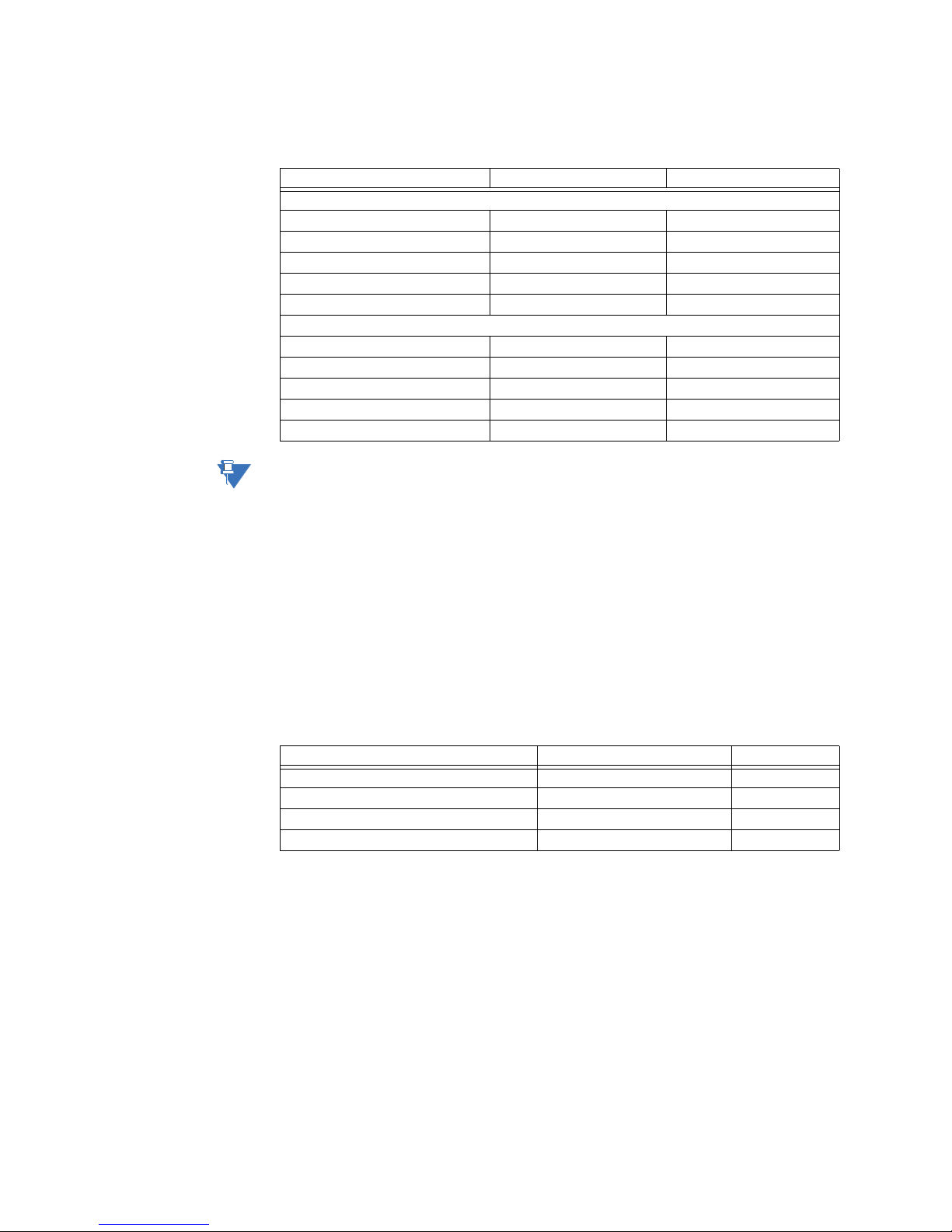
ETHERNET INTERFACE CHAPTER 1: COMMUNICATIONS GUIDE
NOTE
IEC 60870-5-104
protocol settings
NOTE:
Select the Settings > Communications > IEC 60870-5-104 > Protocol menu item to open
the IEC 60870-5-104 protocol configuration window.
Settings Range Default
GENERAL
IEC 60870-5-104 Function Disabled, Enabled Disabled
IEC TCP Port 1 to 65535 2404
IEC Common Address of ASDU 0 to 65535 0
IEC Cyclic Data Period 0 to 65535 s 60 s
IEC TCP Connection Timeout 10 to 300 s 120 s
CLIENT ADDRESS
Client Address 1* 0.0.0.0
Client Address 2* 0.0.0.0
Client Address 3* 0.0.0.0
Client Address 4* 0.0.0.0
Client Address 5* 0.0.0.0
The Client Address setpoints marked "*" are shared with DNP, as only one protocol can be
active at a time.
The 345 can be used as an IEC 60870-5-104 slave device connected to a maximum of two
masters (usually either an RTU or a SCADA master station). Since the 345 maintains two
sets of IEC 60870-5-104 data change buffers, no more than two masters should actively
communicate with the 345 at one time. Five client address settings are used to filter which
master is suitable for communicating with 345.
The IEC 60870-5-104 and DNP protocols cannot be used simultaneously. When the IEC
60870-5-104 FUNCTION setting is set to “Enabled”, the DNP protocol will not be
operational.
If IEC Cyclic Data Period is set to 0 there will be no cyclic data response.
Some other settings can be added to select the first address of the different Object
Information. These settings can be removed to be consistent with the UR but are very
useful for integrating the relay into a system.
Settings Range Default
Object Information Address Binary 1 to 16777215 1000
Object Information Address Analog 1 to 16777215 2000
Object Information Address Counters 1 to 16777215 3000
Object Information Address Command 1 to 16777215 4000
By default, the Object Information Address for the different data will be as follows:
M_SP (Single Points) = 1000
M_ME (Measured Value) = 2000
M_IT (Integrated Totals) = 3000
C_SC or C_DC (Single or Double Command) = 4000
IEC 60870-5-104 point
lists
The Single Points (M_SP) can be configured to a maximum of 64 points. The value for each
point is user-programmable and can be configured by assigning FlexLogic™ operands.
Up to 32 Measured values (M_ME) can be configured assigning FlexAnalog parameters to
each data point.
The Commands points (C_SC or C_DC) can be configured to a maximum of 16 points
selecting data from a list of Virtual Inputs and Force Coil commands.
The table below shows all the Configurable Points settings:
1–58 345 TRANSFORMER PROTECTION SYSTEM – COMMUNICATIONS GUIDE
Page 63

CHAPTER 1: COMMUNICATIONS GUIDE ETHERNET INTERFACE
NOTE
Settings Range Default
Binary Input Point 0 Entry* FlexLogic Operands 0
Binary Input Point 63 Entry* FlexLogic Operands 0
Analog Input Point 0 Entry* 0 to 28 0
Analog Input Point 0 Scale Factor* 0.001, 0.01, 0.1, 1, 10, 100, 1000, 10000,
Analog Input Point 0 Deadband* 0 to 100000000 30000
Analog Input Point 31 Entry* 0 to 28 0
Analog Input Point 31 Scale Factor* 0.001, 0.01, 0.1, 1, 10, 100, 1000, 10000,
Analog Input Point 31 Deadband* 0 to 100000000 30000
Binary Output Point 0 ON* Virtual Input 1 to 32 and Force Coils 0
Binary Output Point 0 OFF* Virtual Input 1 to 32 and Force Coils 0
Binary Output Point 15 ON* Virtual Input 1 to 32 and Force Coils 0
Binary Output Point 15 OFF* Virtual Input 1 to 32 and Force Coils 0
NOTE:
The settings marked "*" are the same as those used by the DNP 3.0 protocol to configure
100000
100000
1
1
the point mapping from address 43878 to 44101.
The IEC 60870-5-104 Deadbands settings are used to determine when to trigger
spontaneous responses containing M_ME_NB_1 analog data. Each setting represents the
threshold value for each M_ME_NB_1 analog point.
For example, to trigger spontaneous responses from the 345 when a current value
changes by 15 A, the "Analog Point xx Deadband" setting should be set to 15. Note that
these settings are the default values of the deadbands. P_ME_NB_1 (parameter of
measured value, scaled value) points can be used to change threshold values from the
default, for each individual M_ME_NB_1 analog point.
There are three ways to send the measurands to the Master station. As the measurands
will be part of the General Group and Group 2, when a general interrogation or group 2
interrogation takes place, all the measurands will be included in the response. There is also
a cyclic data period setting where the scan period is configured to send the measurands to
the Master. The final way is to send the measurands spontaneously when a deadband
overflow takes place.
Groups of Data
The data will be organized in groups in order to provide values when the controlling station
requests by general or group interrogation.
Group 1 will be set by the 64 Single Points(M_SP).
Group 2 will be set by the 32 Measured values (M_ME).
These 64 Single Points and 32 Measured Values will also be sent as a response to a General
Interrogation.
Integrated Totals (M_IT) will have its own Counter Group 1 and these will be sent as a
response to a General Request Counter
345 TRANSFORMER PROTECTION SYSTEM – COMMUNICATIONS GUIDE 1–59
Page 64

ETHERNET INTERFACE CHAPTER 1: COMMUNICATIONS GUIDE
Summary of Ethernet client connections
Table 27: Case A
Settings Ethernet
DNP CHANNEL 1 PORT NONE
DNP CHANNEL 2 PORT NONE
104 GENERAL FUNCTION DISABLE
Client 1 Client 2 Client 3
MODBUS NOTHING NOTHING
MODBUS MODBUS NOTHING
MODBUS MODBUS MODBUS
Table 28: Case B
Settings Ethernet
DNP CHANNEL 1 PORT TCP
DNP CHANNEL 2 PORT NONE
104 GENERAL FUNCTION DISABLE
Client 1 Client 2 Client 3
DNP NOTHING NOTHING
DNP MODBUS NOTHING
DNP MODBUS MODBUS
Table 29: Case C
Settings Ethernet
DNP CHANNEL 1 PORT UDP
DNP CHANNEL 2 PORT NONE
104 GENERAL FUNCTION DISABLE
Client 1 Client 2 Client 3 Client 4
DNP NOTHING NOTHING NOTHING
DNP MODBUS NOTHING NOTHING
DNP MODBUS MODBUS NOTHING
DNP MODBUS MODBUS MODBUS
Table 30: Case D
Settings Ethernet
DNP CHANNEL 1 PORT TCP
DNP CHANNEL 2 PORT TCP
104 GENERAL FUNCTION DISABLE
Client 1 Client 2 Client 3
DNP DNP NOTHING
DNP DNP MODBUS
1–60 345 TRANSFORMER PROTECTION SYSTEM – COMMUNICATIONS GUIDE
Page 65

CHAPTER 1: COMMUNICATIONS GUIDE ETHERNET INTERFACE
Table 31: Case E
Settings Ethernet
DNP CHANNEL 1 PORT TCP
DNP CHANNEL 2 PORT UDP
104 GENERAL FUNCTION DISABLE
Client 1 Client 2 Client 3 Client 4
DNP-TCP DNP-UDP NOTHING NOTHING
DNP-TCP DNP-UDP MODBUS NOTHING
DNP-TCP DNP-UDP MODBUS MODBUS
Table 32: Case F
Settings Ethernet
DNP CHANNEL 1 PORT XX (any
DNP CHANNEL 2 PORT XX (any
104 GENERAL FUNCTION ENABLE
value)
value)
Client 1 Client 2 Client 3
IEC104 IEC104 NOTHING
IEC104 IEC104 MODBUS
345 TRANSFORMER PROTECTION SYSTEM – COMMUNICATIONS GUIDE 1–61
Page 66
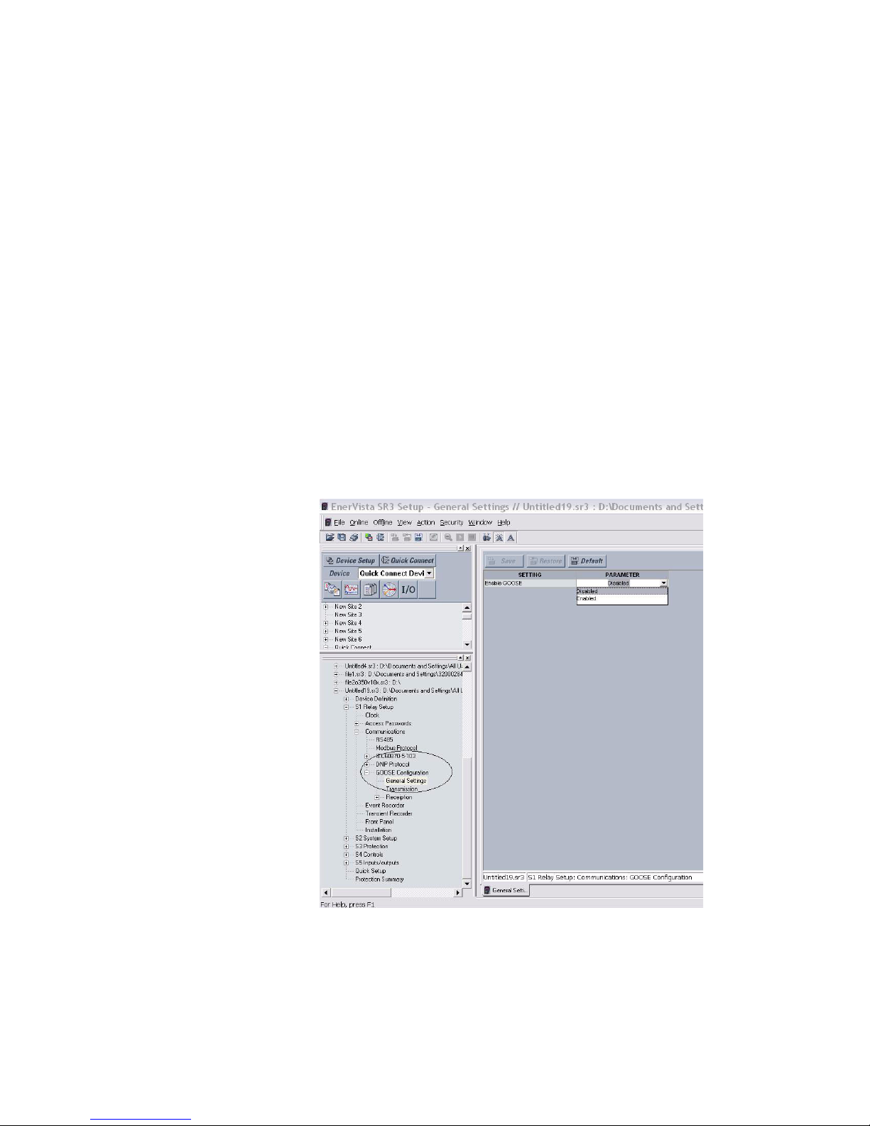
ETHERNET INTERFACE CHAPTER 1: COMMUNICATIONS GUIDE
IEC 61850 GOOSE communications
The 345 firmware supports IEC61850 GOOSE communications on the optional
communications daughter board.
Portions of the IEC61850 standard not pertaining to GOOSE, are not implemented in the
345 relay.
The 345 relay does not support
• an IEC61850 MMS server
• the mapping of analogue values to data points in data sets in either the transmit or
receive direction
• a file system to maintain SCL, ICD or CID files, for IEC61850 GOOSE. As such the
implementation stores GOOSE configuration using MODBUS set points.
Configuration of transmission and reception settings for the GOOSE feature are performed
using EnerVista SR3 Setup Software.
The 345 firmware accepts GOOSE messages from UR, F650 and UR Plus. The
interoperability with other manufacturers will be guaranteed in almost all cases, by
implementing the reception side with nested structures (one level of nesting) and all the
standard data types.
GOOSE settings changes will take effect only after the 345 relay is re-booted. One setting is
available to Enable/Disable both Transmission and Reception. It is possible to change this
setting from the Front Panel of the relay.
Figure 1: EnerVista SR3 GOOSE General Settings
EnerVista SR3 Setup
software structure
1–62 345 TRANSFORMER PROTECTION SYSTEM – COMMUNICATIONS GUIDE
The structure below reflects how the EnerVista SR3 Setup software should be used to
implement the sections detailed in this document , in order to enable both transmission
and reception of GOOSE messages.
Page 67
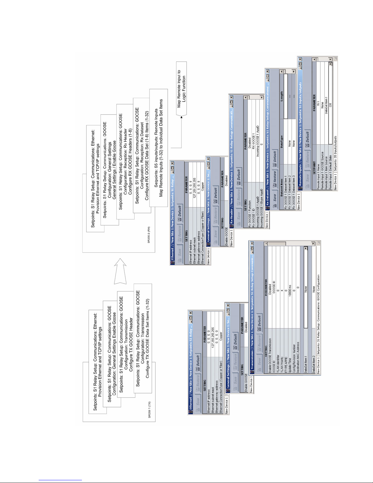
CHAPTER 1: COMMUNICATIONS GUIDE ETHERNET INTERFACE
345 TRANSFORMER PROTECTION SYSTEM – COMMUNICATIONS GUIDE 1–63
Page 68
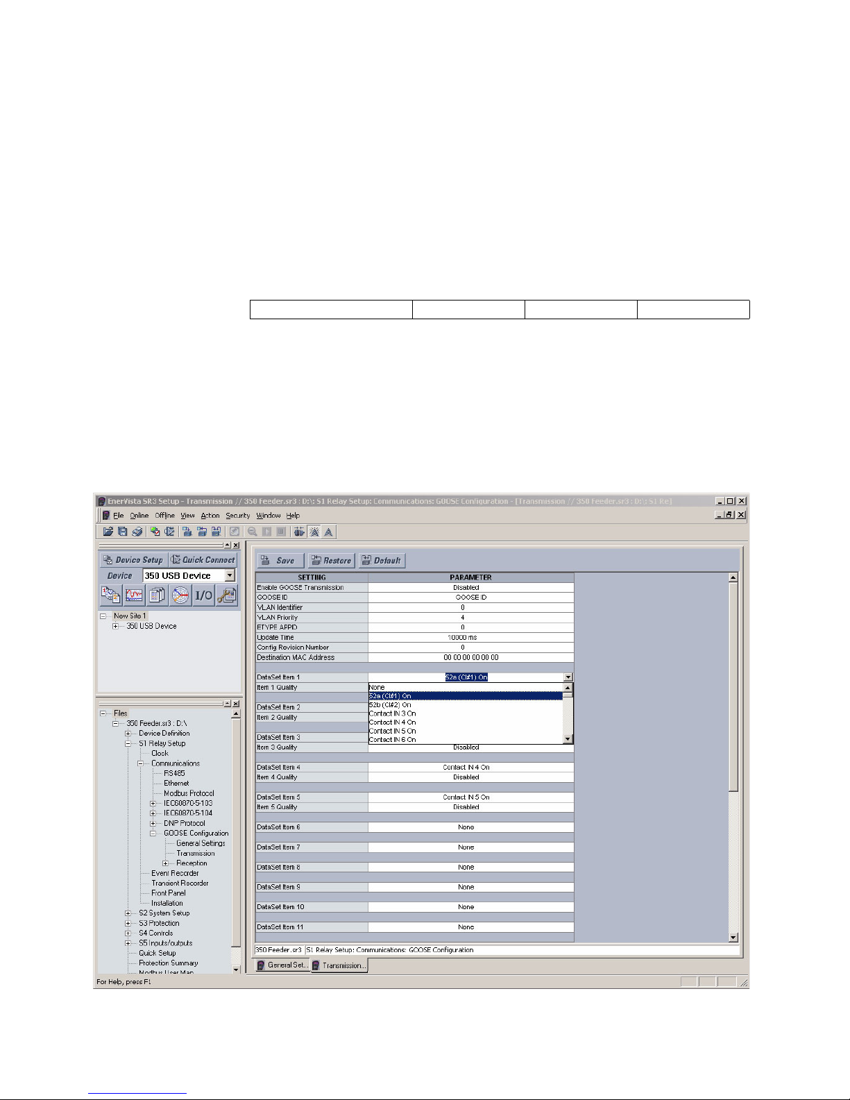
ETHERNET INTERFACE CHAPTER 1: COMMUNICATIONS GUIDE
GOOSE transmission The 345 firmware supports one transmission dataset.
All elements in the transmit dataset must be Booleans values.
The user can define the number of items in the transmit data setup, to a maximum of 32.
The minimum number of items in a data set is 1.
The number of data items configured before the NULL (below), determines the dataset
length. It is also possible to map any Item to a fixed value (ON or OFF).
For GOOSE transmission the firmware allows users to assign, (through EnerVista SR3
Setup Software) an DataSetReference composed as follows:
1. IEDNameLDInst/LLN0$
2. the string (default: GOOSE1) contained in the Modbus address:
eDataSetName 44671 123E DATASET NAME
The IEDName is taken from setting S1 Relay Setup > Installation > Relay Name
Setting the IEDName to "Feeder_25Kv_Line1" (for example) would result in a DataSet
Reference:
Feeder_25Kv_Line1LDInts/LLN0$GOOSE1
Another, less common, possibility is to change the 123E setting ( using modbus ) for
example to "GOOSE_Points" resulting in a DataSet Reference:
Feeder_25Kv_Line1LDInts/LLN0$GOOSE_Points
Figure 2: EnerVista SR3 GOOSE Transmission page
1–64 345 TRANSFORMER PROTECTION SYSTEM – COMMUNICATIONS GUIDE
Page 69

CHAPTER 1: COMMUNICATIONS GUIDE ETHERNET INTERFACE
• GOOSE ID: A string of up to 40 characters that represent the IEC 61850 GOOSE
application ID (GoID). This string identifies the GOOSE Tx message to the receiving
device.
• VLAN Identifier/Priority: a two-byte value whose 3 most significant bits define the
user priority and the twelve least significant bits are for the VLAN identifier. I.e. 32768.
• ETYPE AppID ): to select ISO/IEC 8802-3 frames containing GSE Management and
GOOSE messages and to distinguish the application association.
• Update Time: time to delay transmission of the next iteration of a particular GOOSE
message if no value within the message has changed. I.e. 60. Measured in ms.
• Conf Revision Number: This number updates automatically after Tx data set has been
modified and the relay power has been cycled.
• Destination MAC Address: This setting is required to ensuring interoperability as some
vendors require valid range of destination MAC addresses in GOOSE messages.
• Quality Flags: In order to ensure interoperability with some vendors, it has been
added a quality flag associated to a data item. The quality flags item only can be set if
its associated data item is selected. The data type of the quality flags is Bitstring13
and the attribute will always set to value “0” at the protocol level.
All the elements in a dataset can be mapped by the user to any available digital value
within the 345 relay, including:
• Alarm elements
• Protection elements (Pickup, Dropout and Operate of all available protection elements)
• Control element (all available control elements)
• Status of digital inputs
• Status of digital outputs
• Status of virtual inputs
• Status of virtual outputs.
The destination multicast address for GOOSE messages is composed of the MAC address
of the device, with the least significant bit in the most significant byte, set to 1.
The 345 relay does not generate ICD files that describe the format of transmitted GOOSE
items. EnerVista SR3 software is used to generate these files, and the files must contain at
least the following information:
• Mandatory Nodes: LLN0, LPHD, GGIO, etc.
• GOOSE Configuration: Control Block, Dataset, etc.
• Dataset configuration.
Once a GOOSE message is transmitted, it will be retransmitted at an increasing time
interval as follows: 4ms, 8ms, 16ms, and then 1 second.
GOOSE Rx The 345 firmware allows the user to configure up to 8 separate GOOSE messages for
reception. One GOOSE message consists of 2 parts: Header and Dataset. The Header is
used for identification and the Dataset for data handling.
At this point , it is convenient to clarify the difference between Remote GOOSE and Remote
Device. One Remote Device can send more than one GOOSE, so from the reception point of
view, it is not very useful to handle Remote Devices. Instead, it is simpler to deal with
Remote GOOSE messages.
The 345 firmware is able to receive up to a total of 8 remote GOOSE messages transmitted
from up to a maximum of 8 remote devices.
345 TRANSFORMER PROTECTION SYSTEM – COMMUNICATIONS GUIDE 1–65
Page 70

ETHERNET INTERFACE CHAPTER 1: COMMUNICATIONS GUIDE
GOOSE Rx status In order to visualize the status of the incoming GOOSE messages, the following status
registers must be available in the MODBUS memory map:
Data Item SR3 Text MMI Text Value Format
eDataRemoteGOOSEStat
us
eDataRemoteGOOSEHea
derStatus
GOOSE 1 0x0000 0001
GOOSE 2 0x0000 0010
GOOSE 3 0x0000 0100
GOOSE 4 0x0000 1000
GOOSE 5 0x0001 0000
GOOSE 6 0x0010 0000
GOOSE 7 0x0100 0000
GOOSE 8 0x1000 0000
Enum FC215 0x0001 eFMT_GOOSE1 GOOSE 1 RECEIVED
Remote
GOOSE Status
Remote
GOOSE
Header
Status
unsigned 32 bits GOOSE Receive Status Text String
0x0002 eFMT_GOOSE2 GOOSE 2 RECEIVED
0x0004 eFMT_GOOSE3 GOOSE 3 RECEIVED
0x0008 eFMT_GOOSE4 GOOSE 4 RECEIVED
0x0010 eFMT_GOOSE5 GOOSE 5 RECEIVED
0x0020 eFMT_GOOSE6 GOOSE 6 RECEIVED
0x0040 eFMT_GOOSE7 GOOSE 7 RECEIVED
0x0080 eFMT_GOOSE8 GOOSE 8 RECEIVED
REM GOOSE
STAT
REM GOOSE
HDR STAT
0xFFFF
FFFF
0xFFFF
FFFF
Code
FC215 2
FC215 2
Size
in
word
s
Modb
us
Addre
ss
31515
31517
The GOOSE Header Status is set at 1 if all the header’s filters are passed. Otherwise, the
Header Status will be set at 0.
After a GOOSE header is accepted, the 345 firmware either accepts or rejects the
associated dataset. The firmware bases this decision on the R
configured for the header. If both (Header and Dataset structure) are accepted, the Remote
GOOSE Status is set to 1, otherwise it is set to 0. If the header status is never set to 1, then
the associated GOOSE status always remains at 0.
The incoming GOOSE defines the timeout for the next message. GOOSE Header Status is
set to 0 if the next message is not received within the specified amount of time. GOOSE
Status is also set to 0 if the next message is not accepted within the specified amount of
time.
If a GOOSE message is received, and its header has not been configured for reception, the
firmware ignores the message.
It is possible to see this GOOSE status information from the 345 relay front panel.
1–66 345 TRANSFORMER PROTECTION SYSTEM – COMMUNICATIONS GUIDE
dataset that has been
X
Page 71
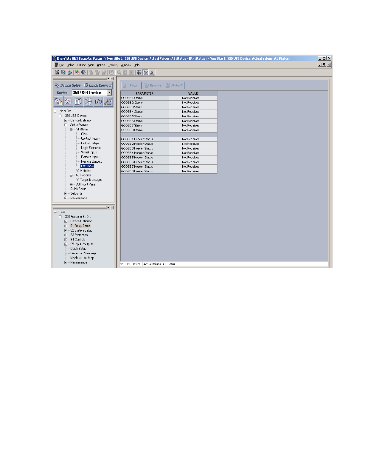
CHAPTER 1: COMMUNICATIONS GUIDE ETHERNET INTERFACE
Figure 3: EnerVista SR3 GOOSE Status page
GOOSE Rx headers The 345 firmware supports GOOSE messages that contain up to one level of nesting, and
that are capable of mapping only digital values to the remote inputs.
The 345 firmware maintains the format of GOOSE messages that can be received in
MODBUS registers.
Configuration of GOOSE messages to be received by the device, is implemented using the
EnerVista SR3 Setup software, as shown below, either by reading in and parsing the ICD, or
SCD file from a remote device, or by manually conf iguring the settings.
345 TRANSFORMER PROTECTION SYSTEM – COMMUNICATIONS GUIDE 1–67
Page 72
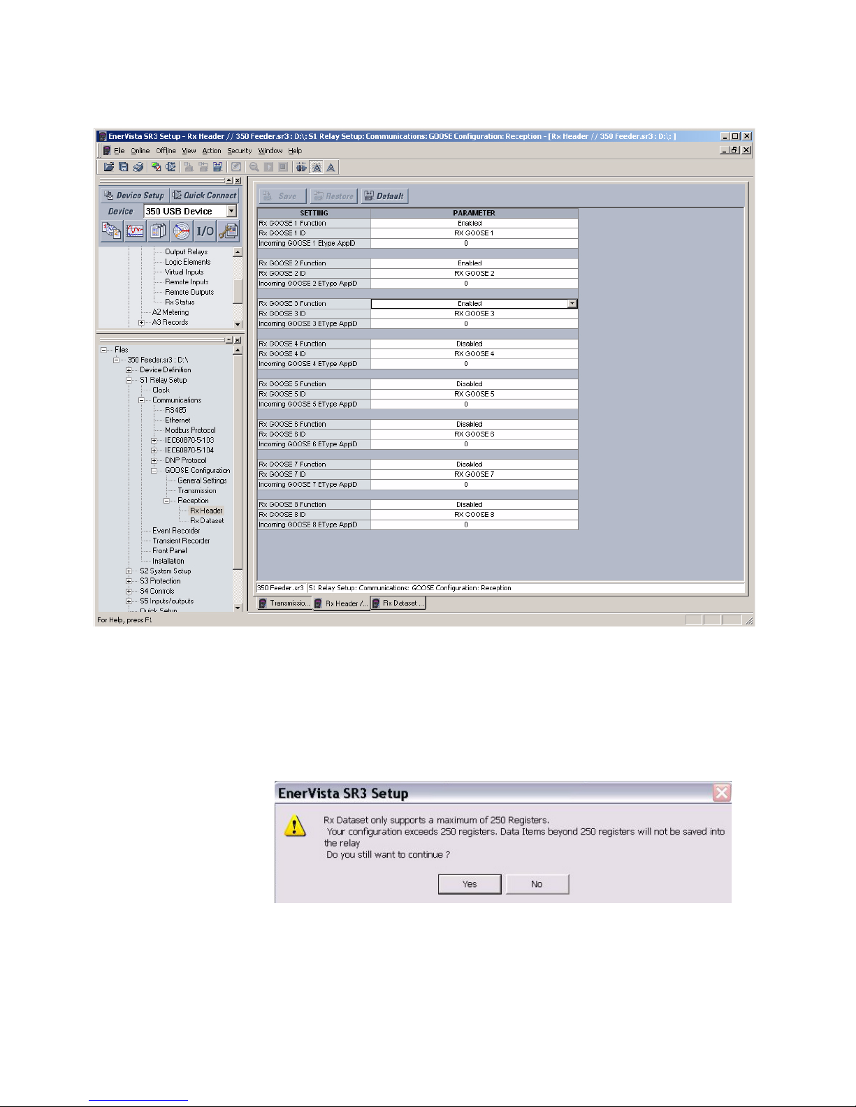
ETHERNET INTERFACE CHAPTER 1: COMMUNICATIONS GUIDE
Figure 4: EnerVista SR3 GOOSE Rx Header
GOOSE receive
dataset structure
The format of the GOOSE messages that can be accepted by the firmware is stored in
MODBUS registers. The maximum total storage size for the 8 Rx GOOSE structure is 250
registers. This means that the number of elements per Rx GOOSE is unlimited provided that
the total size of all Rx structures doesn’t exceed the defined limit of 250 registers.
The User can configure the Datasets of his choice, and if he exceeds the 250 registers limit
when he tries to SAVE, the following message appears, saying that the selection of the user
has exceeded the limit of 250 registers and that anything beyond will be lost.
Clicking on YES will save Dataset items selection up to 250 registers and the others will be
lost. The screen then refreshes, reflecting the saved data. Clicking on NO will do nothing
and the user can make changes on the screen (shown below).
The RX GOOSE message data types that are handled by the software, are:
1–68 345 TRANSFORMER PROTECTION SYSTEM – COMMUNICATIONS GUIDE
Page 73
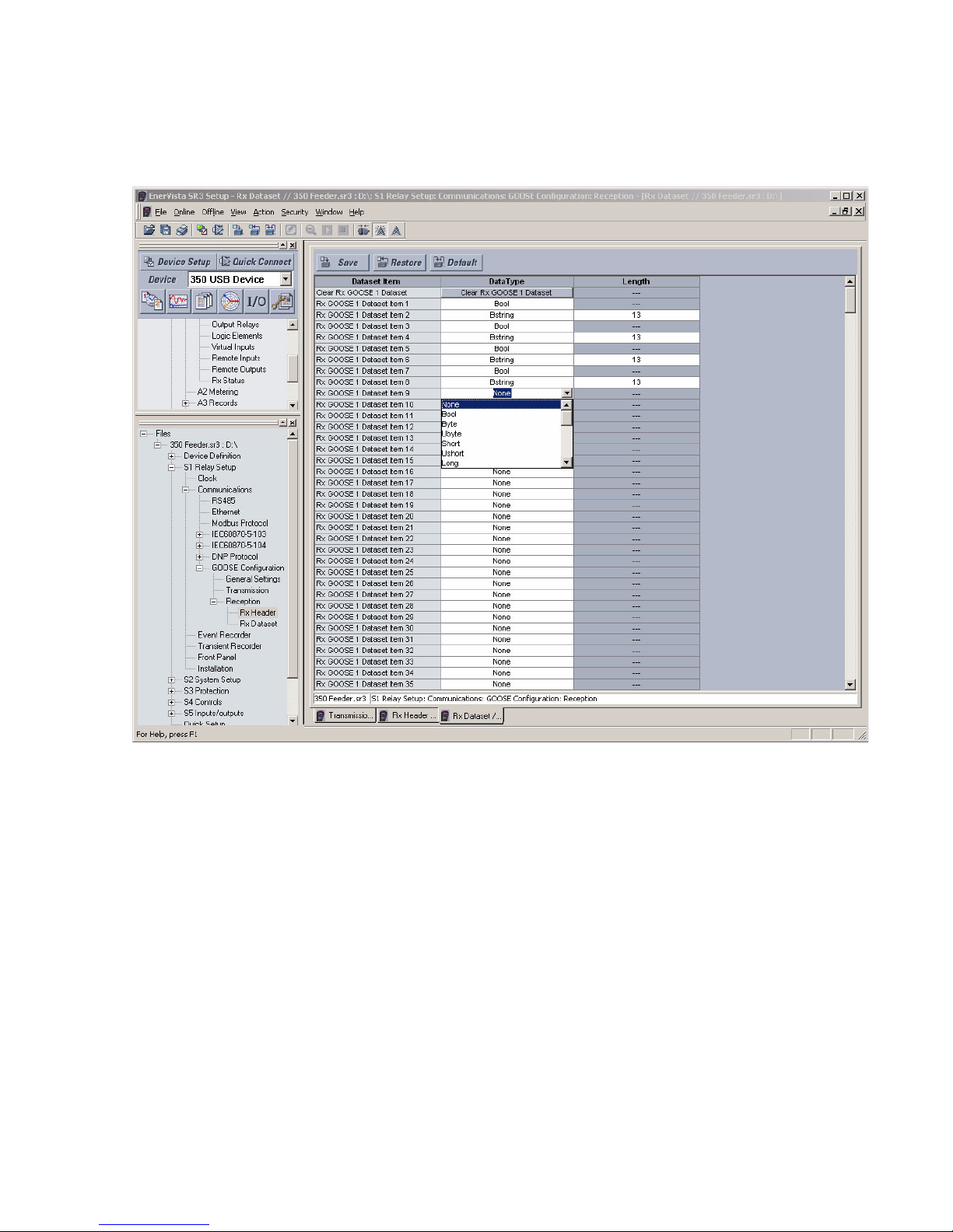
CHAPTER 1: COMMUNICATIONS GUIDE ETHERNET INTERFACE
Bool, Byte, Ubyte, Short , Ushort , Long, Ulong, Int64, Uint64, Float, Double, Btime4, Btime6,
Utctime, Bcd, Vstring, , Ostring, OVstring, Bstring, Bvstring
Figure 5: EnerVista SR3 GOOSE Dataset
GOOSE remote inputs The firmware allows the user to map each of the digital data points received in a data set,
configured for reception, to one of 32 GOOSE remote inputs.
More than 1 GOOSE remote input can be mapped to the same data element, in a data set
belonging to a received GOOSE message.
GOOSE remote inputs can only be mapped to digital data elements.
The firmware considers a GOOSE remote input to be in the “on/off” state when the digital
data element to which it is mapped, is in the “on/off” state.
The firmware allows the user to assign a string name to each of the 32 remote inputs, and
allows the string name assigned to each remote input to be between 1 and 32 characters.
345 TRANSFORMER PROTECTION SYSTEM – COMMUNICATIONS GUIDE 1–69
Page 74
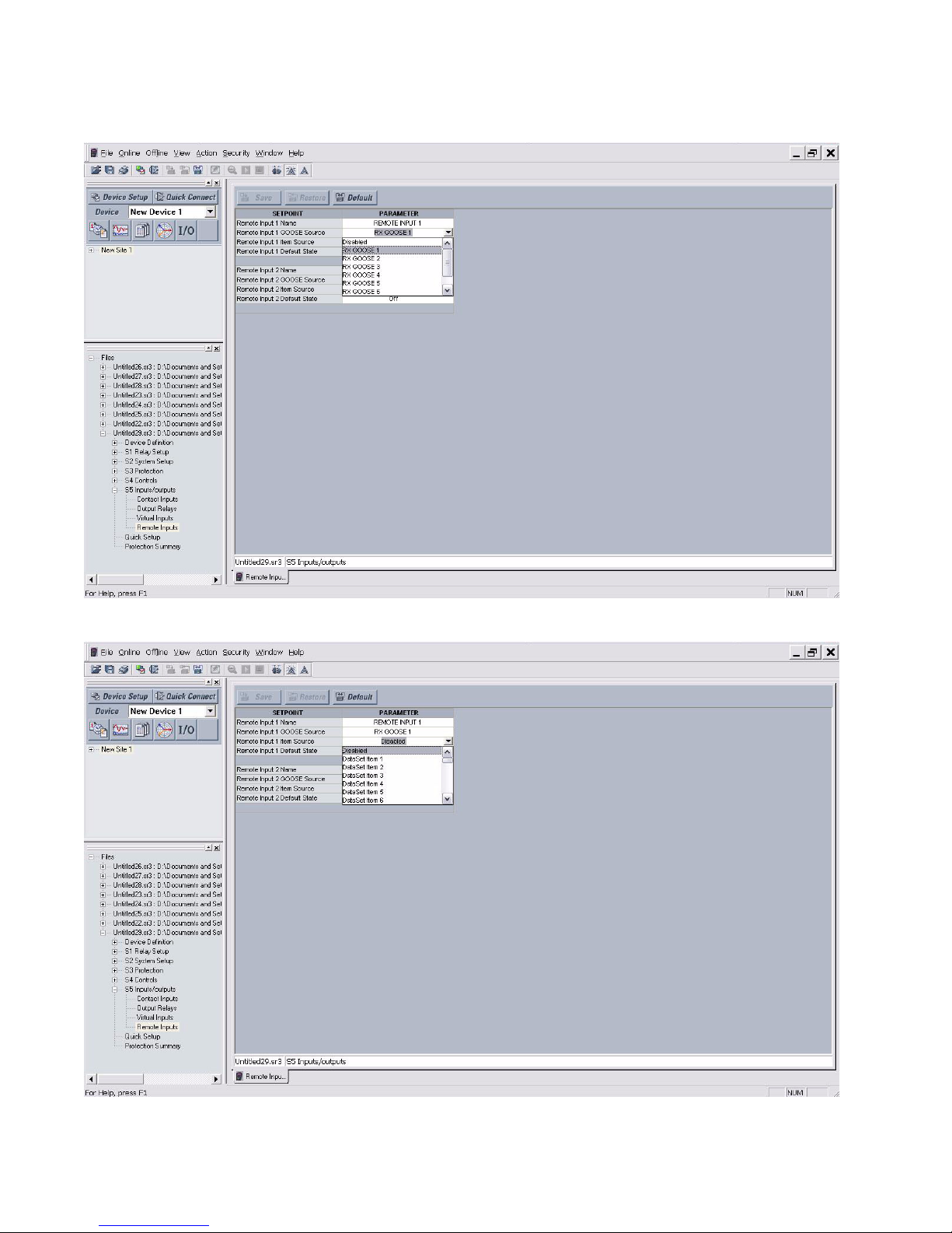
ETHERNET INTERFACE CHAPTER 1: COMMUNICATIONS GUIDE
Figure 6: EnerVista SR3 GOOSE Remote Inputs 1
Figure 7: EnerVista SR3 GOOSE Remote Inputs 2
1–70 345 TRANSFORMER PROTECTION SYSTEM – COMMUNICATIONS GUIDE
Page 75

CHAPTER 1: COMMUNICATIONS GUIDE ETHERNET INTERFACE
The following format indicates the source of the GOOSE message:
The string name of each remote input is maintained in a set of MODBUS registers, where
each string name consumes up to 16 MODBUS registers.
Each GOOSE remote input can be mapped to one of the following functions:
• protection element block (all protection elements that have a single or multiple block
setting)
• group setting change
• user assignable LED
•digital output
The 345 records changes in GOOSE remote inputs in the Event Log.
The time recorded in a GOOSE remote input’s event log entry, is the time at which the
change in the input’s state is detected.
The 345 invokes a logic (block / control) function when its corresponding GOOSE remote
input is asserted.
In the 345 there are many different settings where it is possible to select between a
Contact Input (1 to 8 ), a Virtual Input (1 to 32 ) or a Logic Element (1 to 8 ). In all of these
settings it is also possible to select Remote Input (1-32 ) if the GOOSE feature is enabled on
the relay.
345 TRANSFORMER PROTECTION SYSTEM – COMMUNICATIONS GUIDE 1–71
Page 76

USB INTERFACE CHAPTER 1: COMMUNICATIONS GUIDE
USB interface
The USB inferface supports only the Modbus protocol.
For information on using the USB port on the 345 relay, please refer to Chapter 3 of the 345
Instruction Manual.
MODBUS Protocol
The 345 implements a subset of the Modicon Modbus RTU serial communication standard.
The Modbus protocol is hardware-independent. That is, the physical layer can be any of a
variety of standard hardware configurations. This includes USB, RS485, fibre optics, etc.
Modbus is a single master / multiple slave type of protocol suitable for a multi-drop
configuration.
The 345 is always a Modbus slave. It can not be programmed as a Modbus master.
Computers or PLCs are commonly programmed as masters.
Both monitoring and control are possible using read and write register commands. Other
commands are supported to provide additional functions.
The Modbus protocol has the following characteristics.
•Address: 1 to 254
• Supported Modbus function codes: 3, 4, 5, 6, 7, 8, 10
Data Frame Format
and Data Rate
One data frame of an asynchronous transmission to or from a 345 typically consists of 1
start bit, 8 data bits, and 1 stop bit . This produces a 10 bit data frame. This is important for
transmission through modems at high bit rates.
Modbus protocol can be implemented at any standard communication speed. The 345
supports operation at 9600, 19200, 38400, 57600, and 115200 baud.
Data Packet Format A complete request/response sequence consists of the following bytes (transmitted as
separate data frames):
Master Request Transmission:
SLAVE ADDRESS: 1 byte
FUNCTION CODE: 1 byte
DATA: variable number of bytes depending on FUNCTION CODE
CRC: 2 bytes
Slave Response Transmission:
SLAVE ADDRESS: 1 byte
FUNCTION CODE: 1 byte
DATA: variable number of bytes depending on FUNCTION CODE
CRC: 2 bytes
SLAVE ADDRESS: This is the first byte of every transmission. This byte represents the userassigned address of the slave device that is to receive the message sent by the master.
Each slave device must be assigned a unique address and only the addressed slave will
respond to a transmission that starts with its address. In a master request transmission the
SLAVE ADDRESS represents the address of the slave to which the request is being sent. In a
slave response transmission the SLAVE ADDRESS represents the address of the slave that is
sending the response.
FUNCTION CODE: This is the second byte of every transmission. Modbus defines function
codes of 1 to 127.
1–72 345 TRANSFORMER PROTECTION SYSTEM – COMMUNICATIONS GUIDE
Page 77

CHAPTER 1: COMMUNICATIONS GUIDE USB INTERFACE
DATA: This will be a variable number of bytes depending on the FUNCTION CODE. This may
be Actual Values, Setpoints, or addresses sent by the master to the slave or by the slave to
the master.
CRC: This is a two byte error checking code.
Error Checking The RTU version of Modbus includes a two byte CRC-16 (16 bit cyclic redundancy check)
with every transmission. The CRC-16 algorithm essentially treats the entire data stream
(data bits only; start, stop and parity ignored) as one continuous binary number. This
number is first shifted left 16 bits and then divided by a characteristic polynomial
(11000000000000101B). The 16 bit remainder of the division is appended to the end of the
transmission, MSByte first. The resulting message including CRC, when divided by the
same polynomial at the receiver will give a zero remainder if no transmission errors have
occurred.
If a 345 Modbus slave device receives a transmission in which an error is indicated by the
CRC-16 calculation, the slave device will not respond to the transmission. A CRC-16 error
indicates than one or more bytes of the transmission were received incorrectly and thus
the entire transmission should be ignored in order to avoid the 345 performing any
incorrect operation.
The CRC-16 calculation is an industry standard method used for error detection. An
algorithm is included here to assist programmers in situations where no standard CRC-16
calculation routines are available.
CRC-16 Algorithm Once the following algorithm is complete, the working register “A” will contain the CRC
value to be transmitted. Note that this algorithm requires the characteristic polynomial to
be reverse bit ordered. The MSBit of the characteristic polynomial is dropped since it does
not affect the value of the remainder. The following symbols are used in the algorithm:
—>: data transfer
A: 16 bit working register
AL: low order byte of A
AH: high order byte of A
CRC: 16 bit CRC-16 value
i, j: loop counters
(+): logical exclusive or operator
Di: i-th data byte (i = 0 to N-1)
G: 16 bit characteristic polynomial = 1010000000000001 with MSbit dropped and bit order
reversed
shr(x): shift right (the LSbit of the low order byte of x shifts into a carry flag, a '0' is shifted
into the MSbit of the high order byte of x, all other bits shift right one location
The algorithm is:
1. FFFF hex —> A
2. 0 —> i
3. 0 —> j
345 TRANSFORMER PROTECTION SYSTEM – COMMUNICATIONS GUIDE 1–73
4. Di (+) AL —> AL
5. j+1 —> j
6. shr(A)
7. is there a carry? No: go to 8. Yes: G (+) A —> A
8. is j = 8? No: go to 5. Yes: go to 9.
Page 78

USB INTERFACE CHAPTER 1: COMMUNICATIONS GUIDE
9. i+1 —> i
10. is i = N? No: go to 3. Yes: go to 11.
11. A —> CRC
Timing Data packet synchronization is maintained by timing constraints. The receiving device
must measure the time between the reception of characters. If 3.5 character times elapse
without a new character or completion of the packet, then the communication link must
be reset (i.e. all slaves start listening for a new transmission from the master). Thus at 9600
baud a delay of greater than 3.5 x 1 / 9600 x 10 x = x 3.65 x ms will cause the
communication link to be reset.
345 supported
functions
The following functions are supported by the 345:
• FUNCTION CODE 03 - Read Setpoints
• FUNCTION CODE 04 - Read Actual Values
• FUNCTION CODE 05 - Execute Operation
• FUNCTION CODE 06 - Store Single Setpoint
• FUNCTION CODE 07 - Read Device Status
• FUNCTION CODE 08 - Loopback Test
• FUNCTION CODE 10 - Store Multiple Setpoints
Refer to section 5 of this guide for more details on MODBUS function codes.
1–74 345 TRANSFORMER PROTECTION SYSTEM – COMMUNICATIONS GUIDE
Page 79

CHAPTER 1: COMMUNICATIONS GUIDE MODBUS MEMORY MAP
MODBUS memory map
Modbus
Address
ACTUAL VALUES
PRODUCT INFORMATION
30001 0 Product Device Code 0 1 1 F22 0
30002 1 Hardware Revision 1 26 1 F15 1
30003 2 Firmware Version 0 0xFFFF 1 F3 130
30006 5 Boot Version 0 0xFFFF 1 F3 100
30008 7 Serial Number 0 6 1 F22 1
30014 D Order Code 0 16 1 F22 2
30030 1D MAC Address 0 0xFFFF 1 FC214 0
30037 24 Build Date 0 6 1 F22 23
30043 2A Build Time 0 4 1 F22 23
30049 30 Last Calibration Date 0x010107D8 0X0C1F082E 1 F18 0x010107D8
30051 32 Comm Build Date 0 6 1 F22 23
30057 38 Comm Build T ime 0 4 1 F22 23
30061 3C Comm Rev 0 0xFFFF 1 F3 130
30063 3E Comm Boot Code Rev 0 0xFFFF 1 F3 175
30068 43 FPGA Rev 0 0xFFFF 1 F3 0
30135 86 Main Boot Code Date 0 6 1 F22 23
30141 8C Main Boot Code Time 0 4 1 F22 23
30145 90 Comm Boot Code Date 0 6 1 F22 23
30151 96 Comm Boot Code T ime 0 4 1 F22 23
LAST TRIP DATA
30186 B9 Cause of Last Trip 0 59 1 FC134 0
REAL-TIME CLOCK
30223 DE Weekday 0 7 1 None 0
30224 DF Date Read Only 0x010107D9 0x0C1F0833 0 F18 0x010107D9
30226 E1 Time Read Only 0 0X173B3B63 0 F19 0
30228 E3 Daylight Savings Active 0 1 1 FC126 0
INPUTS/OUTPUTS
30285 11C Contact Input 32-1 (Bit Field) 0 0xFFFFFFFF 1 FC167 0
30288 11F Virtual Input 32-1 (Bit Field) 0 0xFFFFFFFF 1 FC167 0
30290 121 Virtual Output 32-1 (Bit Field) 0 0xFFFFFFFF 1 FC167 0
30296 127 Remote Input 32-1 (Bit Field) 0 0xFFFFFFFF 1 FC167 0
30298 129 Contact Output 32-1 (Bit Field) 0 0xFFFFFFFF 1 FC167 0
30300 12B Remote Output 32-1 (Bit Field) 0 0xFFFFFFFF 1 FC167 0
DEVICE STATUS
30302 12D Current Security Access Level 0 3 1 F1 0
30305 130 Device Status 0 0xFFFF 1 FC129 0
30317 13C Active Setpoint Group 0 1 1 F1 0
30319 13E RELAY1 COIL STATUS 0 1 1 FC125 0
Hex
Address
Description Min Max Step Format
Code
Factory
Default
345 TRANSFORMER PROTECTION SYSTEM – COMMUNICATIONS GUIDE 1–75
Page 80

MODBUS MEMORY MAP CHAPTER 1: COMMUNICATIONS GUIDE
Modbus
Address
Hex
Address
Description Min Max Step Format
Code
30320 13F RELAY2 COIL STATUS 0 1 1 FC125 0
30321 140 TRIP COIL BKR2 STATUS 0 1 1 FC125 0
WINDING 1 CURRENT METERING
30324 143 Sensitive Ground Current 0 0xFFFFFFFF 1 F11 0
30326 145 In 0 100000 1 F10 0
30328 147 Ia 0 100000 1 F10 0
30330 149 Ib 0 100000 1 F10 0
30332 14B Ic 0 100000 1 F10 0
30338 151 Ig 0 500000 1 F10 0
30343 156 Ia Angle 0 359 1 F1 0
30344 157 Ib Angle 0 359 1 F1 0
30345 158 Ic Angle 0 359 1 F1 0
30349 15C Ig Angle 0 359 1 F1 0
30350 15D In Angle 0 359 1 F1 0
30437 1B4 Ph A Thermal Cap 0 1500 1 F2 0
30438 1B5 Ph B Thermal Cap 0 1500 1 F2 0
30439 1B6 Ph C Thermal Cap 0 1500 1 F2 0
30457 1C8 Neg Seq I Angle 0 359 1 F1 0
30478 1DD Neg Seq I Mag 0 65535 1 F2 0
LED STATUS
30505 1F8 LED Status 0 0xFFFFFFFF 1 FC144B 0
INTERNAL FAULT CAUSE
30522 209 Internal Fault Cause 0 0xFFFFFFFF 1 FC188 0
USER MAP ACTUAL VALUES
30524 20B User Map Value 1 0 0xFFFF 1 F1 0
30525 20C User Map Value 2 0 0xFFFF 1 F1 0
30526 20D User Map Value 3 0 0xFFFF 1 F1 0
30527 20E User Map Value 4 0 0xFFFF 1 F1 0
30528 20F User Map Value 5 0 0xFFFF 1 F1 0
30529 210 User Map Value 6 0 0xFFFF 1 F1 0
30530 211 User Map Value 7 0 0xFFFF 1 F1 0
30531 212 User Map Value 8 0 0xFFFF 1 F1 0
30532 213 User Map Value 9 0 0xFFFF 1 F1 0
30533 214 User Map Value 10 0 0xFFFF 1 F1 0
30534 215 User Map Value 11 0 0xFFFF 1 F1 0
30535 216 User Map Value 12 0 0xFFFF 1 F1 0
30536 217 User Map Value 13 0 0xFFFF 1 F1 0
30537 218 User Map Value 14 0 0xFFFF 1 F1 0
30538 219 User Map Value 15 0 0xFFFF 1 F1 0
30539 21A User Map Value 16 0 0xFFFF 1 F1 0
30540 21B User Map Value 17 0 0xFFFF 1 F1 0
30541 21C User Map Value 18 0 0xFFFF 1 F1 0
30542 21D User Map Value 19 0 0xFFFF 1 F1 0
30543 21E User Map Value 20 0 0xFFFF 1 F1 0
30544 21F User Map Value 21 0 0xFFFF 1 F1 0
30545 220 User Map Value 22 0 0xFFFF 1 F1 0
Factory
Default
1–76 345 TRANSFORMER PROTECTION SYSTEM – COMMUNICATIONS GUIDE
Page 81

CHAPTER 1: COMMUNICATIONS GUIDE MODBUS MEMORY MAP
Modbus
Address
Hex
Address
Description Min Max Step Format
Code
30546 221 User Map Value 23 0 0xFFFF 1 F1 0
30547 222 User Map Value 24 0 0xFFFF 1 F1 0
30548 223 User Map Value 25 0 0xFFFF 1 F1 0
30549 224 User Map Value 26 0 0xFFFF 1 F1 0
30550 225 User Map Value 27 0 0xFFFF 1 F1 0
30551 226 User Map Value 28 0 0xFFFF 1 F1 0
30552 227 User Map Value 29 0 0xFFFF 1 F1 0
30553 228 User Map Value 30 0 0xFFFF 1 F1 0
30554 229 User Map Value 31 0 0xFFFF 1 F1 0
30555 22A User Map Value 32 0 0xFFFF 1 F1 0
30556 22B User Map Value 33 0 0xFFFF 1 F1 0
30557 22C User Map Value 34 0 0xFFFF 1 F1 0
30558 22D User Map Value 35 0 0xFFFF 1 F1 0
30559 22E User Map Value 36 0 0xFFFF 1 F1 0
30560 22F User Map Value 37 0 0xFFFF 1 F1 0
30561 230 User Map Value 38 0 0xFFFF 1 F1 0
30562 231 User Map Value 39 0 0xFFFF 1 F1 0
30563 232 User Map Value 40 0 0xFFFF 1 F1 0
30564 233 User Map Value 41 0 0xFFFF 1 F1 0
30565 234 User Map Value 42 0 0xFFFF 1 F1 0
30566 235 User Map Value 43 0 0xFFFF 1 F1 0
30567 236 User Map Value 44 0 0xFFFF 1 F1 0
30568 237 User Map Value 45 0 0xFFFF 1 F1 0
30569 238 User Map Value 46 0 0xFFFF 1 F1 0
30570 239 User Map Value 47 0 0xFFFF 1 F1 0
30571 23A User Map Value 48 0 0xFFFF 1 F1 0
30572 23B User Map Value 49 0 0xFFFF 1 F1 0
30573 23C User Map Value 50 0 0xFFFF 1 F1 0
30574 23D User Map Value 51 0 0xFFFF 1 F1 0
30575 23E User Map Value 52 0 0xFFFF 1 F1 0
30576 23F User Map Value 53 0 0xFFFF 1 F1 0
30577 240 User Map Value 54 0 0xFFFF 1 F1 0
30578 241 User Map Value 55 0 0xFFFF 1 F1 0
30579 242 User Map Value 56 0 0xFFFF 1 F1 0
30580 243 User Map Value 57 0 0xFFFF 1 F1 0
30581 244 User Map Value 58 0 0xFFFF 1 F1 0
30582 245 User Map Value 59 0 0xFFFF 1 F1 0
30583 246 User Map Value 60 0 0xFFFF 1 F1 0
30584 247 User Map Value 61 0 0xFFFF 1 F1 0
30585 248 User Map Value 62 0 0xFFFF 1 F1 0
30586 249 User Map Value 63 0 0xFFFF 1 F1 0
30587 24A User Map Value 64 0 0xFFFF 1 F1 0
30588 24B User Map Value 65 0 0xFFFF 1 F1 0
30589 24C User Map Value 66 0 0xFFFF 1 F1 0
30590 24D User Map Value 67 0 0xFFFF 1 F1 0
30591 24E User Map Value 68 0 0xFFFF 1 F1 0
Factory
Default
345 TRANSFORMER PROTECTION SYSTEM – COMMUNICATIONS GUIDE 1–77
Page 82

MODBUS MEMORY MAP CHAPTER 1: COMMUNICATIONS GUIDE
Modbus
Address
Hex
Address
Description Min Max Step Format
Code
30592 24F User Map Value 69 0 0xFFFF 1 F1 0
30593 250 User Map Value 70 0 0xFFFF 1 F1 0
30594 251 User Map Value 71 0 0xFFFF 1 F1 0
30595 252 User Map Value 72 0 0xFFFF 1 F1 0
30596 253 User Map Value 73 0 0xFFFF 1 F1 0
30597 254 User Map Value 74 0 0xFFFF 1 F1 0
30598 255 User Map Value 75 0 0xFFFF 1 F1 0
30599 256 User Map Value 76 0 0xFFFF 1 F1 0
30600 257 User Map Value 77 0 0xFFFF 1 F1 0
30601 258 User Map Value 78 0 0xFFFF 1 F1 0
30602 259 User Map Value 79 0 0xFFFF 1 F1 0
30603 25A User Map Value 80 0 0xFFFF 1 F1 0
30604 25B User Map Value 81 0 0xFFFF 1 F1 0
30605 25C User Map Value 82 0 0xFFFF 1 F1 0
30606 25D User Map Value 83 0 0xFFFF 1 F1 0
30607 25E User Map Value 84 0 0xFFFF 1 F1 0
30608 25F User Map Value 85 0 0xFFFF 1 F1 0
30609 260 User Map Value 86 0 0xFFFF 1 F1 0
30610 261 User Map Value 87 0 0xFFFF 1 F1 0
30611 262 User Map Value 88 0 0xFFFF 1 F1 0
30612 263 User Map Value 89 0 0xFFFF 1 F1 0
30613 264 User Map Value 90 0 0xFFFF 1 F1 0
30614 265 User Map Value 91 0 0xFFFF 1 F1 0
30615 266 User Map Value 92 0 0xFFFF 1 F1 0
30616 267 User Map Value 93 0 0xFFFF 1 F1 0
30617 268 User Map Value 94 0 0xFFFF 1 F1 0
30618 269 User Map Value 95 0 0xFFFF 1 F1 0
30619 26A User Map Value 96 0 0xFFFF 1 F1 0
30620 26B User Map Value 97 0 0xFFFF 1 F1 0
30621 26C User Map Value 98 0 0xFFFF 1 F1 0
30622 26D User Map Value 99 0 0xFFFF 1 F1 0
30623 26E User Map Value 100 0 0xFFFF 1 F1 0
30624 26F User Map Value 101 0 0xFFFF 1 F1 0
30625 270 User Map Value 102 0 0xFFFF 1 F1 0
30626 271 User Map Value 103 0 0xFFFF 1 F1 0
30627 272 User Map Value 104 0 0xFFFF 1 F1 0
30628 273 User Map Value 105 0 0xFFFF 1 F1 0
30629 274 User Map Value 106 0 0xFFFF 1 F1 0
30630 275 User Map Value 107 0 0xFFFF 1 F1 0
30631 276 User Map Value 108 0 0xFFFF 1 F1 0
30632 277 User Map Value 109 0 0xFFFF 1 F1 0
30633 278 User Map Value 110 0 0xFFFF 1 F1 0
30634 279 User Map Value 111 0 0xFFFF 1 F1 0
30635 27A User Map Value 112 0 0xFFFF 1 F1 0
30636 27B User Map Value 113 0 0xFFFF 1 F1 0
30637 27C User Map Value 114 0 0xFFFF 1 F1 0
Factory
Default
1–78 345 TRANSFORMER PROTECTION SYSTEM – COMMUNICATIONS GUIDE
Page 83

CHAPTER 1: COMMUNICATIONS GUIDE MODBUS MEMORY MAP
Modbus
Address
Hex
Address
Description Min Max Step Format
Code
Factory
Default
30638 27D User Map Value 115 0 0xFFFF 1 F1 0
30639 27E User Map Value 116 0 0xFFFF 1 F1 0
30640 27F User Map Value 117 0 0xFFFF 1 F1 0
30641 280 User Map Value 118 0 0xFFFF 1 F1 0
30642 281 User Map Value 119 0 0xFFFF 1 F1 0
30643 282 User Map Value 120 0 0xFFFF 1 F1 0
30644 283 User Map Value 121 0 0xFFFF 1 F1 0
30645 284 User Map Value 122 0 0xFFFF 1 F1 0
30646 285 User Map Value 123 0 0xFFFF 1 F1 0
30647 286 User Map Value 124 0 0xFFFF 1 F1 0
30648 287 User Map Value 125 0 0xFFFF 1 F1 0
EVENT RECORDER
30659 292 Event Recorder Last Reset 2
0x010107D8 0X0C1F082E 0 F18 0x010107D8
words
30661 294 Total Number of Events Since
0 65535 1 F1 0
Last Clear
30662 295 Cause 0 65535 1 FC134 0
30663 296 Time 0 0X173B3B63 0 F19 0
30665 298 Date 0x010107D8 0X0C1F082E 0 F18 0x010107D8
30667 29A W1 Ia 0 65535 1 F3 0
30668 29B W1 Ib 0 65535 1 F3 0
30669 29C W1 Ic 0 65535 1 F3 0
30670 29D W1 Ig 0 65535 1 F3 0
30671 29E W1 Igd 0 65535 1 F3 0
30672 29F W1 Igr 0 65535 1 F3 0
30673 2A0 W1 I_2 0 65535 1 F3 0
30674 2A1 W1 Ia Angle 0 359 1 F1 0
30675 2A2 W1 Ib Angle 0 359 1 F1 0
30676 2A3 W1 Ic Angle 0 359 1 F1 0
30677 2A4 W1 Ig Angle 0 359 1 F1 0
30678 2A5 W1 In 0 65535 1 F3 0
30679 2A6 W1 In Angle 0 359 1 F1 0
30680 2A7 W2 Ia 0 65535 1 F3 0
30681 2A8 W2 Ib 0 65535 1 F3 0
30682 2A9 W2 Ic 0 65535 1 F3 0
30683 2AA W2 Ig 0 65535 1 F3 0
30684 2AB W2 Igd 0 65535 1 F3 0
30685 2AC W2 Igr 0 65535 1 F3 0
30686 2AD W2 I_2 0 65535 1 F3 0
30687 2AE W2 Ia Angle 0 359 1 F1 0
30688 2AF W2 Ib Angle 0 359 1 F1 0
30689 2B0 W2 Ic Angle 0 359 1 F1 0
30690 2B1 W2 Ig Angle 0 359 1 F1 0
30691 2B2 W2 In 0 65535 1 F3 0
30692 2B3 W2 In Angle 0 359 1 F1 0
30693 2B4 Ph A Diff. 0 65535 1 F3 0
30694 2B5 Ph B Diff. 0 65535 1 F3 0
345 TRANSFORMER PROTECTION SYSTEM – COMMUNICATIONS GUIDE 1–79
Page 84

MODBUS MEMORY MAP CHAPTER 1: COMMUNICATIONS GUIDE
Modbus
Address
Hex
Address
Description Min Max Step Format
Code
Factory
Default
30695 2B6 Ph C Diff. 0 65535 1 F3 0
30696 2B7 Ph A Restr. 0 65535 1 F3 0
30697 2B8 PH A THERMAL CAP 0 1500 1 F2 0
30697 2B8 Ph B Restr. 0 65535 1 F3 0
30698 2B9 PH B THERMAL CAP 0 1500 1 F2 0
30698 2B9 Ph C Restr. 0 65535 1 F3 0
30699 2BA PH C THERMAL CAP 0 1500 1 F2 0
30699 2BA 2nd Harm Ph A diff 0 65535 1 F2 0
30700 2BB 2nd Harm Ph B diff 0 65535 1 F2 0
30701 2BC 2nd Harm Ph C diff 0 65535 1 F2 0
30702 2BD Thermal Capacity A 0 1500 1 F2 0
30703 2BE Thermal Capacity B 0 1500 1 F2 0
30704 2BF Thermal Capacity C 0 1500 1 F2 0
30705 2C0 Self-Test Event 0 0xFFFFFFFF 2 FC188 0
TRANSIENT RECORDER
30707 2C2 Transient Recorder Last Cleared 0x010107D8 0X0C1F082E 0 F18 0x010107D8
30709 2C4 Transient Recorder Available
0 65535 1 F1 0
Records
30710 2C5 Trigger Date 0x010107D8 0X0C1F082E 0 F18 0x010107D8
30712 2C7 Trigger Time 0 0X173B3B63 0 F19 0
30714 2C9 Trigger Cause 0 0xD002 0 FC133 0
30715 2CA Trigger Frequency 20 120 1 F3 60
30716 2CB Total Triggers 0 0xFFFF 1 F1 0
30718 2CD Trigger Position 0 100 1 F1 25
30719 2CE Trace Memory Start Index 0 6143 1 F1 0
30720 2CF Sample Index + Trace Memory
-32767 32767 1 F4 0
Sample 1
30721 2D0 Sample Index + Trace Memory
-32767 32767 1 F4 0
Sample 2
30722 2D1 Sample Index + Trace Memory
-32767 32767 1 F4 0
Sample 3
30723 2D2 Sample Index + Trace Memory
-32767 32767 1 F4 0
Sample 4
30724 2D3 Sample Index + Trace Memory
-32767 32767 1 F4 0
Sample 5
30725 2D4 Sample Index + Trace Memory
-32767 32767 1 F4 0
Sample 6
30726 2D5 Sample Index + Trace Memory
-32767 32767 1 F4 0
Sample 7
30727 2D6 Sample Index + Trace Memory
-32767 32767 1 F4 0
Sample 8
30728 2D7 Sample Index + Trace Memory
-32767 32767 1 F4 0
Sample 9
30729 2D8 Sample Index + Trace Memory
-32767 32767 1 F4 0
Sample 10
30730 2D9 Sample Index + Trace Memory
-32767 32767 1 F4 0
Sample 11
30731 2DA Sample Index + Trace Memory
-32767 32767 1 F4 0
Sample 12
30732 2DB Sample Index + Trace Memory
-32767 32767 1 F4 0
Sample 13
1–80 345 TRANSFORMER PROTECTION SYSTEM – COMMUNICATIONS GUIDE
Page 85

CHAPTER 1: COMMUNICATIONS GUIDE MODBUS MEMORY MAP
Modbus
Address
Hex
Address
Description Min Max Step Format
30733 2DC Sample Index + Trace Memory
Sample 14
30734 2DD Sample Index + Trace Memory
Sample 15
30735 2DE Sample Index + Trace Memory
Sample 16
30736 2DF Sample Index + Trace Memory
Sample 17
30737 2E0 Sample Index + Trace Memory
Sample 18
30738 2E1 Sample Index + Trace Memory
Sample 19
30739 2E2 Sample Index + Trace Memory
Sample 20
30740 2E3 Sample Index + Trace Memory
Sample 21
30741 2E4 Sample Index + Trace Memory
Sample 22
30742 2E5 Sample Index + Trace Memory
Sample 23
30743 2E6 Sample Index + Trace Memory
Sample 24
30744 2E7 Sample Index + Trace Memory
Sample 25
30745 2E8 Sample Index + Trace Memory
Sample 26
30746 2E9 Sample Index + Trace Memory
Sample 27
30747 2EA Sample Index + Trace Memory
Sample 28
30748 2EB Sample Index + Trace Memory
Sample 29
30749 2EC Sample Index + Trace Memory
Sample 30
30750 2ED Sample Index + Trace Memory
Sample 31
30751 2EE Sample Index + Trace Memory
Sample 32
30752 2EF Sample Index + Trace Memory
Sample 33
30753 2F0 Sample Index + Trace Memory
Sample 34
30754 2F1 Sample Index + Trace Memory
Sample 35
30755 2F2 Sample Index + Trace Memory
Sample 36
30756 2F3 Sample Index + Trace Memory
Sample 37
30757 2F4 Sample Index + Trace Memory
Sample 38
30758 2F5 Sample Index + Trace Memory
Sample 39
30759 2F6 Sample Index + Trace Memory
Sample 40
30760 2F7 Sample Index + Trace Memory
Sample 41
Code
-32767 32767 1 F4 0
-32767 32767 1 F4 0
-32767 32767 1 F4 0
-32767 32767 1 F4 0
-32767 32767 1 F4 0
-32767 32767 1 F4 0
-32767 32767 1 F4 0
-32767 32767 1 F4 0
-32767 32767 1 F4 0
-32767 32767 1 F4 0
-32767 32767 1 F4 0
-32767 32767 1 F4 0
-32767 32767 1 F4 0
-32767 32767 1 F4 0
-32767 32767 1 F4 0
-32767 32767 1 F4 0
-32767 32767 1 F4 0
-32767 32767 1 F4 0
-32767 32767 1 F4 0
-32767 32767 1 F4 0
-32767 32767 1 F4 0
-32767 32767 1 F4 0
-32767 32767 1 F4 0
-32767 32767 1 F4 0
-32767 32767 1 F4 0
-32767 32767 1 F4 0
-32767 32767 1 F4 0
-32767 32767 1 F4 0
Factory
Default
345 TRANSFORMER PROTECTION SYSTEM – COMMUNICATIONS GUIDE 1–81
Page 86

MODBUS MEMORY MAP CHAPTER 1: COMMUNICATIONS GUIDE
Modbus
Address
Hex
Address
Description Min Max Step Format
30761 2F8 Sample Index + Trace Memory
Sample 42
30762 2F9 Sample Index + Trace Memory
Sample 43
30763 2FA Sample Index + Trace Memory
Sample 44
30764 2FB Sample Index + Trace Memory
Sample 45
30765 2FC Sample Index + Trace Memory
Sample 46
30766 2FD Sample Index + Trace Memory
Sample 47
30767 2FE Sample Index + Trace Memory
Sample 48
30768 2FF Sample Index + Trace Memory
Sample 49
30769 300 Sample Index + Trace Memory
Sample 50
30770 301 Sample Index + Trace Memory
Sample 51
30771 302 Sample Index + Trace Memory
Sample 52
30772 303 Sample Index + Trace Memory
Sample 53
30773 304 Sample Index + Trace Memory
Sample 54
30774 305 Sample Index + Trace Memory
Sample 55
30775 306 Sample Index + Trace Memory
Sample 56
30776 307 Sample Index + Trace Memory
Sample 57
30777 308 Sample Index + Trace Memory
Sample 58
30778 309 Sample Index + Trace Memory
Sample 59
30779 30A Sample Index + Trace Memory
Sample 60
30780 30B Sample Index + Trace Memory
Sample 61
30781 30C Sample Index + Trace Memory
Sample 62
30782 30D Sample Index + Trace Memory
Sample 63
30783 30E Sample Index + Trace Memory
Sample 64
30784 30F Sample Index + Trace Memory
Sample 65
30785 310 Sample Index + Trace Memory
Sample 66
30786 311 Sample Index + Trace Memory
Sample 67
30787 312 Sample Index + Trace Memory
Sample 68
30788 313 Sample Index + Trace Memory
Sample 69
Code
-32767 32767 1 F4 0
-32767 32767 1 F4 0
-32767 32767 1 F4 0
-32767 32767 1 F4 0
-32767 32767 1 F4 0
-32767 32767 1 F4 0
-32767 32767 1 F4 0
-32767 32767 1 F4 0
-32767 32767 1 F4 0
-32767 32767 1 F4 0
-32767 32767 1 F4 0
-32767 32767 1 F4 0
-32767 32767 1 F4 0
-32767 32767 1 F4 0
-32767 32767 1 F4 0
-32767 32767 1 F4 0
-32767 32767 1 F4 0
-32767 32767 1 F4 0
-32767 32767 1 F4 0
-32767 32767 1 F4 0
-32767 32767 1 F4 0
-32767 32767 1 F4 0
-32767 32767 1 F4 0
-32767 32767 1 F4 0
-32767 32767 1 F4 0
-32767 32767 1 F4 0
-32767 32767 1 F4 0
-32767 32767 1 F4 0
Factory
Default
1–82 345 TRANSFORMER PROTECTION SYSTEM – COMMUNICATIONS GUIDE
Page 87

CHAPTER 1: COMMUNICATIONS GUIDE MODBUS MEMORY MAP
Modbus
Address
Hex
Address
Description Min Max Step Format
30789 314 Sample Index + Trace Memory
Sample 70
30790 315 Sample Index + Trace Memory
Sample 71
30791 316 Sample Index + Trace Memory
Sample 72
30792 317 Sample Index + Trace Memory
Sample 73
30793 318 Sample Index + Trace Memory
Sample 74
30794 319 Sample Index + Trace Memory
Sample 75
30795 31A Sample Index + Trace Memory
Sample 76
30796 31B Sample Index + Trace Memory
Sample 77
30797 31C Sample Index + Trace Memory
Sample 78
30798 31D Sample Index + Trace Memory
Sample 79
30799 31E Sample Index + Trace Memory
Sample 80
30800 31F Sample Index + Trace Memory
Sample 81
30801 320 Sample Index + Trace Memory
Sample 82
30802 321 Sample Index + Trace Memory
Sample 83
30803 322 Sample Index + Trace Memory
Sample 84
30804 323 Sample Index + Trace Memory
Sample 85
30805 324 Sample Index + Trace Memory
Sample 86
30806 325 Sample Index + Trace Memory
Sample 87
30807 326 Sample Index + Trace Memory
Sample 88
30808 327 Sample Index + Trace Memory
Sample 89
30809 328 Sample Index + Trace Memory
Sample 90
30810 329 Sample Index + Trace Memory
Sample 91
30811 32A Sample Index + Trace Memory
Sample 92
30812 32B Sample Index + Trace Memory
Sample 93
30813 32C Sample Index + Trace Memory
Sample 94
30814 32D Sample Index + Trace Memory
Sample 95
30815 32E Sample Index + Trace Memory
Sample 96
30816 32F Sample Index + Trace Memory
Sample 97
Code
-32767 32767 1 F4 0
-32767 32767 1 F4 0
-32767 32767 1 F4 0
-32767 32767 1 F4 0
-32767 32767 1 F4 0
-32767 32767 1 F4 0
-32767 32767 1 F4 0
-32767 32767 1 F4 0
-32767 32767 1 F4 0
-32767 32767 1 F4 0
-32767 32767 1 F4 0
-32767 32767 1 F4 0
-32767 32767 1 F4 0
-32767 32767 1 F4 0
-32767 32767 1 F4 0
-32767 32767 1 F4 0
-32767 32767 1 F4 0
-32767 32767 1 F4 0
-32767 32767 1 F4 0
-32767 32767 1 F4 0
-32767 32767 1 F4 0
-32767 32767 1 F4 0
-32767 32767 1 F4 0
-32767 32767 1 F4 0
-32767 32767 1 F4 0
-32767 32767 1 F4 0
-32767 32767 1 F4 0
-32767 32767 1 F4 0
Factory
Default
345 TRANSFORMER PROTECTION SYSTEM – COMMUNICATIONS GUIDE 1–83
Page 88

MODBUS MEMORY MAP CHAPTER 1: COMMUNICATIONS GUIDE
Modbus
Address
Hex
Address
Description Min Max Step Format
30817 330 Sample Index + Trace Memory
Sample 98
30818 331 Sample Index + Trace Memory
Sample 99
30819 332 Sample Index + Trace Memory
Sample 100
30820 333 Sample Index + Trace Memory
Sample 101
30821 334 Sample Index + Trace Memory
Sample 102
30822 335 Sample Index + Trace Memory
Sample 103
30823 336 Sample Index + Trace Memory
Sample 104
30824 337 Sample Index + Trace Memory
Sample 105
30825 338 Sample Index + Trace Memory
Sample 106
30826 339 Sample Index + Trace Memory
Sample 107
30827 33A Sample Index + Trace Memory
Sample 108
30828 33B Sample Index + Trace Memory
Sample 109
30829 33C Sample Index + Trace Memory
Sample 110
30830 33D Sample Index + Trace Memory
Sample 111
30831 33E Sample Index + Trace Memory
Sample 112
30832 33F Sample Index + Trace Memory
Sample 113
30833 340 Sample Index + Trace Memory
Sample 114
30834 341 Sample Index + Trace Memory
Sample 115
30835 342 Sample Index + Trace Memory
Sample 116
30836 343 Sample Index + Trace Memory
Sample 117
30837 344 Sample Index + Trace Memory
Sample 118
30838 345 Sample Index + Trace Memory
Sample 119
30839 346 Sample Index + Trace Memory
Sample 120
30840 347 Sample Index + Trace Memory
Sample 121
30841 348 Sample Index + Trace Memory
Sample 122
30842 349 Sample Index + Trace Memory
Sample 123
30843 34A Sample Index + Trace Memory
Sample 124
30844 34B Sample Index + Trace Memory
Sample 125
Code
-32767 32767 1 F4 0
-32767 32767 1 F4 0
-32767 32767 1 F4 0
-32767 32767 1 F4 0
-32767 32767 1 F4 0
-32767 32767 1 F4 0
-32767 32767 1 F4 0
-32767 32767 1 F4 0
-32767 32767 1 F4 0
-32767 32767 1 F4 0
-32767 32767 1 F4 0
-32767 32767 1 F4 0
-32767 32767 1 F4 0
-32767 32767 1 F4 0
-32767 32767 1 F4 0
-32767 32767 1 F4 0
-32767 32767 1 F4 0
-32767 32767 1 F4 0
-32767 32767 1 F4 0
-32767 32767 1 F4 0
-32767 32767 1 F4 0
-32767 32767 1 F4 0
-32767 32767 1 F4 0
-32767 32767 1 F4 0
-32767 32767 1 F4 0
-32767 32767 1 F4 0
-32767 32767 1 F4 0
-32767 32767 1 F4 0
Factory
Default
1–84 345 TRANSFORMER PROTECTION SYSTEM – COMMUNICATIONS GUIDE
Page 89

CHAPTER 1: COMMUNICATIONS GUIDE MODBUS MEMORY MAP
Modbus
Address
30845 34C Sample Index + Trace Memory
Hex
Address
Description Min Max Step Format
Code
-32767 32767 1 F4 0
Sample 126
30846 34D Sample Index + Trace Memory
-32767 32767 1 F4 0
Sample 127
30847 34E Sample Index + Trace Memory
-32767 32767 1 F4 0
Sample 128
STATUS BUFFER
30946 3B1 Alarm Status 4 0 0xFFFFFFFF 1 FC182 0
30948 3B3 Alarm Status 3 0 0xFFFFFFFF 1 FC181 0
30950 3B5 Alarm Status 2 0 0xFFFFFFFF 1 FC180 0
30952 3B7 Alarm Status 1 0 0xFFFFFFFF 1 FC179 0
30954 3B9 Trip Status 4 0 0xFFFFFFFF 1 FC186 0
30956 3BB Trip Status 3 0 0xFFFFFFFF 1 FC185 0
30958 3BD Trip Status 2 0 0xFFFFFFFF 1 FC184 0
30960 3BF Trip Status 1 0 0xFFFFFFFF 1 FC183 0
30962 3C1 Message Status 4 0 0xFFFFFFFF 1 FC190 0
30964 3C3 Message Status 3 0 0xFFFFFFFF 1 FC189 0
30966 3C5 Message Status 2 0 0xFFFFFFFF 1 FC188 0
30968 3C7 Message Status 1 0 0xFFFFFFFF 1 FC187 0
30970 3C9 Ctrl Element Status 4 0 0xFFFFFFFF 1 FC194 0
30972 3CB Ctrl Element Status 3 0 0xFFFFFFFF 1 FC193 0
30974 3CD Ctrl Element Status 2 0 0xFFFFFFFF 1 FC192 0
30976 3CF Ctrl Element Status 1 0 0xFFFFFFFF 1 FC191 0
30978 3D1 Block Status 4 0 0xFFFFFFFF 1 FC203 0
30980 3D3 Block Status 3 0 0xFFFFFFFF 1 FC202 0
30982 3D5 Block Status 2 0 0xFFFFFFFF 1 FC201 0
30984 3D7 Block Status 1 0 0xFFFFFFFF 1 FC200 0
IEC61850 GOOSE STATUS
31515 5EA REM GOOSE STAT 0 0xFFFFFFFF 1 FC215 0
31517 5EC REM GOOSE HDR STAT 0 0xFFFFFFFF 1 FC215 0
THERMAL MODEL TRIP STATUS
31521 5F0 Trip Phase A Status 1 0 65535 1 FC134 0
31522 5F1 Trip Phase B Status 1 0 65535 1 FC134 0
31523 5F2 Trip Phase C Status 1 0 65535 1 FC134 0
PHASE IOC1 TRIP STATUS
31524 5F3 Trip Phase A Status 2 0 65535 1 FC134 0
31525 5F4 Trip Phase B Status 2 0 65535 1 FC134 0
31526 5F5 Trip Phase C Status 2 0 65535 1 FC134 0
PHASE TOC1 TRIP STATUS
31527 5F6 Trip Phase A Status 3 0 65535 1 FC134 0
31528 5F7 Trip Phase B Status 3 0 65535 1 FC134 0
31529 5F8 Trip Phase C Status 3 0 65535 1 FC134 0
PHASE IOC2 TRIP STATUS
31530 5F9 Trip Phase A Status 4 0 65535 1 FC134 0
31531 5FA Trip Phase B Status 4 0 65535 1 FC134 0
31532 5FB Trip Phase C Status 4 0 65535 1 FC134 0
DIFFERENTIAL TRIP STATUS
Factory
Default
345 TRANSFORMER PROTECTION SYSTEM – COMMUNICATIONS GUIDE 1–85
Page 90

MODBUS MEMORY MAP CHAPTER 1: COMMUNICATIONS GUIDE
Modbus
Address
Hex
Address
Description Min Max Step Format
Code
31539 602 Diff Trip PhA Status 0 65535 1 FC134 0
31540 603 Diff Trip PhB Status 0 65535 1 FC134 0
31541 604 Diff Trip PhC Status 0 65535 1 FC134 0
PHASE TOC2 TRIP STATUS
31542 605 Phase51PTOC_2Trip_PhaseAStatus0 65535 1 FC134 0
31543 606 Phase51PTOC_2Trip_PhaseBStatus0 65535 1 FC134 0
31544 607 Phase51PTOC_2Trip_PhaseCStatus0 65535 1 FC134 0
THERMAL MODEL ALARM STATUS
31569 620 Alarm Phase A Status 1 0 65535 1 FC134 0
31570 621 Alarm Phase B Status 1 0 65535 1 FC134 0
31571 622 Alarm Phase C Status 1 0 65535 1 FC134 0
PHASE IOC1 ALARM STATUS
31572 623 Alarm Phase A Status 2 0 65535 1 FC134 0
31573 624 Alarm Phase B Status 2 0 65535 1 FC134 0
31574 625 Alarm Phase C Status 2 0 65535 1 FC134 0
PHASE TOC1 ALARM STATUS
31575 626 Alarm Phase A Status 3 0 65535 1 FC134 0
31576 627 Alarm Phase B Status 3 0 65535 1 FC134 0
31577 628 Alarm Phase C Status 3 0 65535 1 FC134 0
PHASE IOC2 ALARM STATUS
31578 629 Alarm Phase A Status 4 0 65535 1 FC134 0
31579 62A Alarm Phase B Status 4 0 65535 1 FC134 0
31580 62B Alarm Phase C Status 4 0 65535 1 FC134 0
DIFFERENTIAL ALARM STATUS
31587 632 Diff Alarm PhA Status 0 65535 1 FC134 0
31588 633 Diff Alarm PhB Status 0 65535 1 FC134 0
31589 634 Diff Alarm PhC Status 0 65535 1 FC134 0
PHASE TOC2 ALARM STATUS
31590 635 Phase51PTOC_2Alarm_PhaseASt
0 65535 1 FC134 0
atus
31591 636 Phase51PTOC_2Alarm_PhaseBSt
0 65535 1 FC134 0
atus
31592 637 Phase51PTOC_2Alarm_PhaseCSt
0 65535 1 FC134 0
atus
WINDING 2 CURRENT METERING
31665 680 Ia2 0 100000 1 F10 0
31667 682 Ib2 0 100000 1 F10 0
31669 684 Ic2 0 100000 1 F10 0
31671 686 In2 0 100000 1 F10 0
31673 688 Ig2 0 100000 1 F10 0
31675 68A Isg2 0 100000 1 F11 0
PHASE DIFFERENTIAL CURRENT METERING
31677 68C Idiff 1 Ph A 0 100000 1 F11 0
31679 68E Idiff 1 Ph B 0 100000 1 F11 0
31681 690 Idiff 1 Ph C 0 100000 1 F11 0
Factory
Default
1–86 345 TRANSFORMER PROTECTION SYSTEM – COMMUNICATIONS GUIDE
Page 91

CHAPTER 1: COMMUNICATIONS GUIDE MODBUS MEMORY MAP
Modbus
Address
Hex
Address
Description Min Max Step Format
Code
31683 692 Idiff 2 Ph A 0 1000 1 F2 0
31684 693 Idiff 2 Ph B 0 1000 1 F2 0
31685 694 Idiff 2 Ph C 0 1000 1 F2 0
31686 695 Idiff 5 Ph A 0 1000 1 F2 0
31687 696 Idiff 5 Ph B 0 1000 1 F2 0
31688 697 Idiff 5 Ph C 0 1000 1 F2 0
RESTRAINT CURRENT METERING
31695 69E I Restraint Ph A 0 100000 1 F11 0
31697 6A0 I Restraint Ph B 0 100000 1 F11 0
31699 6A2 I Restraint Ph C 0 100000 1 F11 0
PHASE ANGLES
31701 6A4 Ia2 Angle 0 359 1 F1 0
31702 6A5 Ib2 Angle 0 359 1 F1 0
31703 6A6 Ic2 Angle 0 359 1 F1 0
31704 6A7 Ig2 Angle 0 359 1 F1 0
31705 6A8 In2 Angle 0 359 1 F1 0
31706 6A9 Idiff 1 PhA Angle 0 359 1 F1 0
31707 6AA Idiff 1 PhB Angle 0 359 1 F1 0
31708 6AB Idiff 1 PhC Angle 0 359 1 F1 0
31709 6AC Idiff 2 PhA Angle 0 359 1 F1 0
31710 6AD Idiff 2 PhB Angle 0 359 1 F1 0
31711 6AE Idiff 2 PhC Angle 0 359 1 F1 0
31712 6AF Idiff 5 PhA Angle 0 359 1 F1 0
31713 6B0 Idiff 5 PhB Angle 0 359 1 F1 0
31714 6B1 Idiff 5 PhC Angle 0 359 1 F1 0
31715 6B2 Irestraint A Angle 0 359 1 F1 0
31716 6B3 Irestraint B Angle 0 359 1 F1 0
31717 6B4 Irestraint C Angle 0 359 1 F1 0
31721 6B8 W2 Neg Seq Angle 0 359 1 F1 0
GROUND DIFFERENTIAL CURRENT METERING
31724 6BB W1 Gnd Dif Current 0 1000000 1 F11 0
31726 6BD W1 Gnd Dif Angle 0 359 1 F1 0
31727 6BE W2 Gnd Dif Current 0 1000000 1 F11 0
31729 6C0 W2 Gnd Dif Angle 0 359 1 F1 0
WINDING 2 NEGATIVE SEQUENCE CURRENT METERING
31730 6C1 W2 Neg Sequence 0 0xFFFF 1 F2 0
Factory
Default
SETPOINTS
MESSAGE TIMES
40120 77 Flash Message T ime 1 65535 1 F1 5
40121 78 Message T imeout 1 65535 1 F1 30
COMMANDS
40129 80 Command address 0 0xFFFF 0 F1 0
40130 81 Command Function 0 0xFFFF 0 F1 0
40131 82 Command Data 1 0 0xFFFF 0 F1 0
345 TRANSFORMER PROTECTION SYSTEM – COMMUNICATIONS GUIDE 1–87
Page 92

MODBUS MEMORY MAP CHAPTER 1: COMMUNICATIONS GUIDE
Modbus
Address
Hex
Address
Description Min Max Step Format
Code
Factory
Default
40132 83 Command Data 2 0 0xFFFF 0 F1 0
40133 84 Command Data 3 0 0xFFFF 0 F1 0
40134 85 Command Data 4 0 0xFFFF 0 F1 0
40135 86 Command Data 5 0 0xFFFF 0 F1 0
40136 87 Command Data 6 0 0xFFFF 0 F1 0
40137 88 Command Data 7 0 0xFFFF 0 F1 0
40138 89 Command Data 8 0 0xFFFF 0 F1 0
40139 8A Command Data 9 0 0xFFFF 0 F1 0
40140 8B Command Data 10 0 0xFFFF 0 F1 0
RS485 COMMUNICATIONS
40172 AB Slave Address 1 254 1 F1 254
40173 AC RS485 Baud Rate 0 4 1 FC101 4
40174 AD RS485 Parity 0 2 1 FC102 0
40175 AE Rear 485 Port Protocol 0 2 1 F97 0
ETHERNET COMMUNICATIONS
40180 B3 SNTP Mode 0 3 1 FC100 0
40181 B4 SNTP IP Address 0 0xFFFFFFFF 1 FC150 0
40183 B6 Ethernet IP address 0 0xFFFFFFFF 1 FC150 0
40185 B8 Ethernet subnet mask 0 0xFFFFFFFF 1 FC150 0xFFFFFC00
40187 BA Ethernet gateway address 0 0xFFFFFFFF 1 FC150 0
40189 BC SNTP Port 0 65535 1 F1 0
40191 BE EthernetConnectionType 0 1 1 FC230 0
REAL-TIME CLOCK
40228 E3 Set Date 0x010107D9 0x0C1F0833 0 F18 0x010107D9
40230 E5 Set Time 0 0X173B3B63 0 F19 0
40232 E7 Time Offset From UTC -2400 2400 25 F6 0
40233 E8 IRIG-B 0 1 1 FC126 0
40234 E9 Daylight Savings 0 1 1 FC126 0
40235 EA DST Start Month 0 12 1 FC169 0
40236 EB DST Start Week 0 5 1 FC170 0
40237 EC DST Start Weekday 0 7 1 FC171 0
40238 ED DST End Month 0 12 1 FC169 0
40239 EE DST End Week 0 5 1 FC170 0
40240 EF DST End Weekday 0 7 1 FC171 0
REMOTE INPUTS
40260 103 Remote Inputs 0 0xFFFFFFFF 1 FC167 0
VIRTUAL INPUTS
40262 105 Virtual Input 32-1 (Bit Field) 0 0xFFFFFFFF 1 FC167 0
POWER SYSTEM
40284 11B Supply Frequency 0 1 1 FC107 0
40285 11C Transformer Name 0 10 1 F22 3
40296 127 Phase Sequence 0 1 1 FC124A 0
USER MAP ADDRESSES
40524 20B User Map Address 1 30001 39999 1 F1 30305
40525 20C User Map Address 2 30001 39999 1 F1 30505
40526 20D User Map Address 3 30001 39999 1 F1 30506
1–88 345 TRANSFORMER PROTECTION SYSTEM – COMMUNICATIONS GUIDE
Page 93

CHAPTER 1: COMMUNICATIONS GUIDE MODBUS MEMORY MAP
Modbus
Address
Hex
Address
Description Min Max Step Format
Code
Factory
Default
40527 20E User Map Address 4 30001 39999 1 F1 30960
40528 20F User Map Address 5 30001 39999 1 F1 30961
40529 210 User Map Address 6 30001 39999 1 F1 30958
40530 211 User Map Address 7 30001 39999 1 F1 30959
40531 212 User Map Address 8 30001 39999 1 F1 30956
40532 213 User Map Address 9 30001 39999 1 F1 30957
40533 214 User Map Address 10 30001 39999 1 F1 30954
40534 215 User Map Address 11 30001 39999 1 F1 30955
40535 216 User Map Address 12 30001 39999 1 F1 30952
40536 217 User Map Address 13 30001 39999 1 F1 30953
40537 218 User Map Address 14 30001 39999 1 F1 30950
40538 219 User Map Address 15 30001 39999 1 F1 30951
40539 21A User Map Address 16 30001 39999 1 F1 30948
40540 21B User Map Address 17 30001 39999 1 F1 30949
40541 21C User Map Address 18 30001 39999 1 F1 30946
40542 21D User Map Address 19 30001 39999 1 F1 30947
40543 21E User Map Address 20 30001 39999 1 F1 30976
40544 21F User Map Address 21 30001 39999 1 F1 30977
40545 220 User Map Address 22 30001 39999 1 F1 30974
40546 221 User Map Address 23 30001 39999 1 F1 30975
40547 222 User Map Address 24 30001 39999 1 F1 30972
40548 223 User Map Address 25 30001 39999 1 F1 30973
40549 224 User Map Address 26 30001 39999 1 F1 30970
40550 225 User Map Address 27 30001 39999 1 F1 30971
40551 226 User Map Address 28 30001 39999 1 F1 30984
40552 227 User Map Address 29 30001 39999 1 F1 30985
40553 228 User Map Address 30 30001 39999 1 F1 30982
40554 229 User Map Address 31 30001 39999 1 F1 30983
40555 22A User Map Address 32 30001 39999 1 F1 30980
40556 22B User Map Address 33 30001 39999 1 F1 30981
40557 22C User Map Address 34 30001 39999 1 F1 30978
40558 22D User Map Address 35 30001 39999 1 F1 30979
40559 22E User Map Address 36 30001 39999 1 F1 30186
40560 22F User Map Address 37 30001 39999 1 F1 30285
40561 230 User Map Address 38 30001 39999 1 F1 30286
40562 231 User Map Address 39 30001 39999 1 F1 30298
40563 232 User Map Address 40 30001 39999 1 F1 30299
40564 233 User Map Address 41 30001 39999 1 F1 30288
40565 234 User Map Address 42 30001 39999 1 F1 30289
40566 235 User Map Address 43 30001 39999 1 F1 30290
40567 236 User Map Address 44 30001 39999 1 F1 30291
40568 237 User Map Address 45 30001 39999 1 F1 30296
40569 238 User Map Address 46 30001 39999 1 F1 30297
40570 239 User Map Address 47 30001 39999 1 F1 30300
40571 23A User Map Address 48 30001 39999 1 F1 30301
40572 23B User Map Address 49 30001 39999 1 F1 30328
345 TRANSFORMER PROTECTION SYSTEM – COMMUNICATIONS GUIDE 1–89
Page 94

MODBUS MEMORY MAP CHAPTER 1: COMMUNICATIONS GUIDE
Modbus
Address
Hex
Address
Description Min Max Step Format
Code
Factory
Default
40573 23C User Map Address 50 30001 39999 1 F1 30329
40574 23D User Map Address 51 30001 39999 1 F1 30330
40575 23E User Map Address 52 30001 39999 1 F1 30331
40576 23F User Map Address 53 30001 39999 1 F1 30332
40577 240 User Map Address 54 30001 39999 1 F1 30333
40578 241 User Map Address 55 30001 39999 1 F1 30326
40579 242 User Map Address 56 30001 39999 1 F1 30327
40580 243 User Map Address 57 30001 39999 1 F1 30338
40581 244 User Map Address 58 30001 39999 1 F1 30339
40582 245 User Map Address 59 30001 39999 1 F1 30324
40583 246 User Map Address 60 30001 39999 1 F1 30325
40584 247 User Map Address 61 30001 39999 1 F1 30319
40585 248 User Map Address 62 30001 39999 1 F1 30320
40586 249 User Map Address 63 30001 39999 1 F1 31665
40587 24A User Map Address 64 30001 39999 1 F1 31666
40588 24B User Map Address 65 30001 39999 1 F1 31667
40589 24C User Map Address 66 30001 39999 1 F1 31668
40590 24D User Map Address 67 30001 39999 1 F1 31669
40591 24E User Map Address 68 30001 39999 1 F1 31670
40592 24F User Map Address 69 30001 39999 1 F1 31671
40593 250 User Map Address 70 30001 39999 1 F1 31672
40594 251 User Map Address 71 30001 39999 1 F1 31673
40595 252 User Map Address 72 30001 39999 1 F1 31674
40596 253 User Map Address 73 30001 39999 1 F1 31675
40597 254 User Map Address 74 30001 39999 1 F1 31676
40598 255 User Map Address 75 30001 39999 1 F1 31677
40599 256 User Map Address 76 30001 39999 1 F1 31678
40600 257 User Map Address 77 30001 39999 1 F1 31679
40601 258 User Map Address 78 30001 39999 1 F1 31680
40602 259 User Map Address 79 30001 39999 1 F1 31681
40603 25A User Map Address 80 30001 39999 1 F1 31682
40604 25B User Map Address 81 30001 39999 1 F1 31683
40605 25C User Map Address 82 30001 39999 1 F1 31684
40606 25D User Map Address 83 30001 39999 1 F1 31685
40607 25E User Map Address 84 30001 39999 1 F1 31686
40608 25F User Map Address 85 30001 39999 1 F1 31687
40609 260 User Map Address 86 30001 39999 1 F1 31688
40610 261 User Map Address 87 30001 39999 1 F1 31695
40611 262 User Map Address 88 30001 39999 1 F1 31696
40612 263 User Map Address 89 30001 39999 1 F1 31697
40613 264 User Map Address 90 30001 39999 1 F1 31698
40614 265 User Map Address 91 30001 39999 1 F1 31699
40615 266 User Map Address 92 30001 39999 1 F1 31700
40616 267 User Map Address 93 30001 39999 1 F1 30001
40617 268 User Map Address 94 30001 39999 1 F1 30001
40618 269 User Map Address 95 30001 39999 1 F1 30001
1–90 345 TRANSFORMER PROTECTION SYSTEM – COMMUNICATIONS GUIDE
Page 95

CHAPTER 1: COMMUNICATIONS GUIDE MODBUS MEMORY MAP
Modbus
Address
Hex
Address
Description Min Max Step Format
Code
Factory
Default
40619 26A User Map Address 96 30001 39999 1 F1 30001
40620 26B User Map Address 97 30001 39999 1 F1 30001
40621 26C User Map Address 98 30001 39999 1 F1 30001
40622 26D User Map Address 99 30001 39999 1 F1 30001
40623 26E User Map Address 100 30001 39999 1 F1 30001
40624 26F User Map Address 101 30001 39999 1 F1 30001
40625 270 User Map Address 102 30001 39999 1 F1 30001
40626 271 User Map Address 103 30001 39999 1 F1 30001
40627 272 User Map Address 104 30001 39999 1 F1 30001
40628 273 User Map Address 105 30001 39999 1 F1 30001
40629 274 User Map Address 106 30001 39999 1 F1 30001
40630 275 User Map Address 107 30001 39999 1 F1 30001
40631 276 User Map Address 108 30001 39999 1 F1 30001
40632 277 User Map Address 109 30001 39999 1 F1 30001
40633 278 User Map Address 110 30001 39999 1 F1 30001
40634 279 User Map Address 111 30001 39999 1 F1 30001
40635 27A User Map Address 112 30001 39999 1 F1 30001
40636 27B User Map Address 113 30001 39999 1 F1 30001
40637 27C User Map Address 114 30001 39999 1 F1 30001
40638 27D User Map Address 115 30001 39999 1 F1 30001
40639 27E User Map Address 116 30001 39999 1 F1 30001
40640 27F User Map Address 117 30001 39999 1 F1 30001
40641 280 User Map Address 118 30001 39999 1 F1 30001
40642 281 User Map Address 119 30001 39999 1 F1 30001
40643 282 User Map Address 120 30001 39999 1 F1 30001
40644 283 User Map Address 121 30001 39999 1 F1 30001
40645 284 User Map Address 122 30001 39999 1 F1 30001
40646 285 User Map Address 123 30001 39999 1 F1 30001
40647 286 User Map Address 124 30001 39999 1 F1 30001
40648 287 User Map Address 125 30001 39999 1 F1 30001
TRANSIENT RECORDER TRIGGERS
40650 289 Trigger On Input 1 0 0x1DF 1 F89 0
40651 28A Trigger On Input 2 0 0x1DF 1 F89 0
40652 28B Trigger On Input 3 0 0x1DF 1 F89 0
EVENT RECORDER
40654 28D Recording of Pickup Events 0 1 1 FC126 1
40655 28E Recording of Contact Input
0 1 1 FC126 1
Events
40656 28F Recording of Virtual Input Events 0 1 1 FC126 1
40657 290 Recording of Remote Inputs 0 1 1 FC126 1
40658 291 Recording of Logic Element
0 1 1 FC126 1
Events
40660 293 Recording of Trip Events 0 1 1 FC126 1
40661 294 Recording of Alarm Events 0 1 1 FC126 1
40662 295 Recording of Control Events 0 1 1 FC126 1
40665 298 Recording of Dropout Events 0 1 1 FC126 0
345 TRANSFORMER PROTECTION SYSTEM – COMMUNICATIONS GUIDE 1–91
Page 96

MODBUS MEMORY MAP CHAPTER 1: COMMUNICATIONS GUIDE
Modbus
Address
40666 299 Recording of Set Time/Date
Hex
Address
Description Min Max Step Format
Code
0 1 1 FC126 0
Events
40667 29A Event Record Selector 1 65535 1 F1 1
TRANSIENT RECORDER
40668 29B Trigger On PKP 0 1 1 FC103 0
40669 29C Trigger On Trip 0 1 1 FC103 0
40670 29D Trigger On Alarm 0 1 1 FC103 0
40671 29E Trigger on DPO 0 1 1 FC103 0
40672 29F Trace Memory Channel Selector 0 16 1 F26 0
40672 29F Trace Memory Channel Selector 0 16 1 F26B 0
40673 2A0 Trace Memory Buffer Selector 0 10 1 F1 0
40674 2A1 Trace Memory Sample Index 0 6144 1 F1 0
40675 2A2 Trigger Source 1 0xD002 1 FC133 1
40676 2A3 Trigger Position 0 100 1 F1 20
40677 2A4 Trigger Mode 0 1 1 FC148 0
40678 2A5 Transient Buffer Setup 0 2 1 F95 0
RELAY STATUS
40927 39E Relay Status 0 1 1 F99 0
CONTACT INPUT NAMES (1 - 8)
40961 3C0 Input Name 1 0 9 1 F22 27
40970 3C9 Input Name 2 0 9 1 F22 28
40979 3D2 Input Name 3 0 9 1 F22 29
40988 3DB Input Name 4 0 9 1 F22 30
40997 3E4 Input Name 5 0 9 1 F22 31
41006 3ED Input Name 6 0 9 1 F22 32
41015 3F6 Input Name 7 0 9 1 F22 33
41024 3FF Input Name 8 0 9 1 F22 34
EDIT SETPOINT GROUP
41113 458 Edit Setpoint Group -1 1 1 F91 0
LOGIC ELEMENTS
41118 45D Timer 1 Pickup Delay 0 6000 1 F1 0
41119 45E Timer 1 Dropout Delay 0 6000 1 F1 0
41120 45F LE 1 Function 0 4 1 FC205 0
41121 460 LE 1 Asserted 0 1 1 FC103 0
41122 461 LE 1 Relays 0 0x7F 1 FC198 0
41126 465 Timer 2 Pickup Delay 0 6000 1 F1 0
41127 466 Timer 2 Dropout Delay 0 6000 1 F1 0
41128 467 LE 2 Function 0 4 1 FC205 0
41129 468 LE 2 Asserted 0 1 1 FC103 0
41130 469 LE 2 Relays 0 0x7F 1 FC198 0
41134 46D Timer 3 Pickup Delay 0 6000 1 F1 0
41135 46E Timer 3 Dropout Delay 0 6000 1 F1 0
41136 46F LE 3 Function 0 4 1 FC205 0
41137 470 LE 3 Asserted 0 1 1 FC103 0
41138 471 LE 3 Relays 0 0x7F 1 FC198 0
41142 475 Timer 4 Pickup Delay 0 6000 1 F1 0
Factory
Default
1–92 345 TRANSFORMER PROTECTION SYSTEM – COMMUNICATIONS GUIDE
Page 97

CHAPTER 1: COMMUNICATIONS GUIDE MODBUS MEMORY MAP
Modbus
Address
Hex
Address
Description Min Max Step Format
Code
41143 476 Timer 4 Dropout Delay 0 6000 1 F1 0
41144 477 LE 4 Function 0 4 1 FC205 0
41145 478 LE 4 Asserted 0 1 1 FC103 0
41146 479 LE 4 Relays 0 0x7F 1 FC198 0
41150 47D Timer 5 Pickup Delay 0 6000 1 F1 0
41151 47E Timer 5 Dropout Delay 0 6000 1 F1 0
41152 47F LE 5 Function 0 4 1 FC205 0
41153 480 LE 5 Asserted 0 1 1 FC103 0
41154 481 LE 5 Relays 0 0x7F 1 FC198 0
41158 485 Timer 6 Pickup Delay 0 6000 1 F1 0
41159 486 Timer 6 Dropout Delay 0 6000 1 F1 0
41160 487 LE 6 Function 0 4 1 FC205 0
41161 488 LE 6 Asserted 0 1 1 FC103 0
41162 489 LE 6 Relays 0 0x7F 1 FC198 0
41166 48D Timer 7 Pickup Delay 0 6000 1 F1 0
41167 48E Timer 7 Dropout Delay 0 6000 1 F1 0
41168 48F LE 7 Function 0 4 1 FC205 0
41169 490 LE 7 Asserted 0 1 1 FC103 0
41170 491 LE 7 Relays 0 0x7F 1 FC198 0
41174 495 Timer 8 Pickup Delay 0 6000 1 F1 0
41175 496 Timer 8 Dropout Delay 0 6000 1 F1 0
41176 497 LE 8 Function 0 4 1 FC205 0
41177 498 LE 8 Asserted 0 1 1 FC103 0
41178 499 LE 8 Relays 0 0x7F 1 FC198 0
REMOTE RESET
41380 563 Remote Reset 0 0x1DF 1 F89 0
WINDING 1 BREAKER
41388 56B Breaker Connected 0 0x49 0 FC204B 0
41389 56C Breaker 52a Contact 0 0x40 0 FC204A 0
41390 56D Breaker 52b Contact 0 0x41 0 FC204C 0
SETPOINT GROUP CHANGE
41404 57B Set Group 2 Active 0 0x1DF 0 F89 0
41405 57C Block Group Change 0 0x1DF 0 F89 0
41410 581 Breaker 1 Connected 0 0x47 0 FC204D 0
WINDING 2 BREAKER
41414 585 Breaker 2 Connected 0 0x49 0 FC204B 0
41415 586 Breaker 2 52a Contact 0 0x42 0 FC204D 0
41416 587 Breaker 2 52b Contact 0 0x43 0 FC204F 0
TRANSFORMER SETUP
41420 58B XFMR Rated MVA 0 5000 1 F11 500
41422 58D XFRM Type 0 25 1 FC419 0
41423 58E Phase Compensation 0 1 1 FC411 0
41424 58F Winding 1 Nominal Voltage 1 6500 1 F11 1380
41426 591 Winding 1 Grounding 0 1 0 FC413 0
41427 592 Winding 2 Nominal Voltage 1 6500 1 F11 416
41429 594 Winding 2 Grounding 0 1 0 FC413 0
Factory
Default
345 TRANSFORMER PROTECTION SYSTEM – COMMUNICATIONS GUIDE 1–93
Page 98

MODBUS MEMORY MAP CHAPTER 1: COMMUNICATIONS GUIDE
Modbus
Address
Hex
Address
Description Min Max Step Format
Code
CONTACT INPUT NAMES (9 - 10)
41435 59A Input Name 9 0 9 1 F22 165
41444 5A3 Input Name 10 0 9 1 F22 166
CONTACT INPUTS
41454 5AD Input 9 Debounce Interval 1 64 1 F1 2
41455 5AE Input 10 Debounce Interval 1 64 1 F1 2
41456 5AF Input 1 Debounce Interval 1 64 1 F1 2
41457 5B0 Input 2 Debounce Interval 1 64 1 F1 2
41458 5B1 Input 3 Debounce Interval 1 64 1 F1 2
41459 5B2 Input 4 Debounce Interval 1 64 1 F1 2
41460 5B3 Input 5 Debounce Interval 1 64 1 F1 2
41461 5B4 Input 6 Debounce Interval 1 64 1 F1 2
41462 5B5 Input 7 Debounce Interval 1 64 1 F1 2
41463 5B6 Input 8 Debounce Interval 1 64 1 F1 2
41465 5B8 Select DC Voltage 0 3 1 FC123 2
FRONT PANEL SETUP
41475 5C2 Screen Saver 0 10000 1 F1C 0
41498 5D9 Breaker Open LED color 0 3 1 FC157 2
41498 5D9 W1 Breaker Open color 0 3 1 FC157 2
41500 5DB W1 Breaker Closed color 0 3 1 FC157 2
41502 5DD W2 Breaker Open color 0 3 1 FC157 2
41504 5DF W2 Breaker Closed color 0 3 1 FC157 2
OUTPUT RELAYS
41510 5E5 Relay 3 Type 0 1 1 FC199 0
41511 5E6 Relay 4 Type 0 1 1 FC199 0
41512 5E7 Relay 5 Type 0 1 1 FC199 0
41513 5E8 Relay 6 Type 0 1 1 FC199 0
41547 60A BLOCK RLY 1 TRIP 0 0x1DF 1 F89 0
41549 60C BLOCK RLY 2 TRIP 0 0x1DF 1 F89 0
COIL MONITORS
42214 8A5 BYPASS BKR STATUS 0 1 1 FC126 0
42215 8A6 Relay1 Coil Monitor Function 0 2 1 FC206 0
42216 8A7 Relay1 Coil Monitor Pickup 1 10 1 F1 5
42217 8A8 Relay1 Coil Monitor Relay 0 0x7F 1 FC198 0
42218 8A9 BYPASS BKR STATUS 0 1 1 FC126 0
42219 8AA Relay2 Coil Monitor Function 0 2 1 FC206 0
42220 8AB Relay2 Coil Monitor Pickup 1 10 1 F1 5
42221 8AC Relay2 Coil Monitor Relay 0 0x7F 1 FC198 0
TRIP RELAY SEAL-IN
42222 8AD RLY 1 SEAL-IN 0 999 1 F3 4
42224 8AF RELAY 2 TRIP SEAL IN: 0 999 1 F3 4
W1 BREAKER FAIL
42262 8D5 Breaker Failure Function 0 2 1 FC206 0
42263 8D6 Breaker Failure Delay 1 3 100 1 F3 10
42264 8D7 Breaker Failure Current 5 2000 1 F3 100
42265 8D8 Breaker Failure Delay 2 0 100 1 F3 0
Factory
Default
1–94 345 TRANSFORMER PROTECTION SYSTEM – COMMUNICATIONS GUIDE
Page 99

CHAPTER 1: COMMUNICATIONS GUIDE MODBUS MEMORY MAP
Modbus
Address
Hex
Address
Description Min Max Step Format
Code
42266 8D9 Breaker Failure Relays 0 0x7F 1 FC198 0
42267 8DA BF EXT INITIATE 0 0x1DF 1 F89 0
PHASE IOC1
42485 9B4 Phase Inst OC Function 0 3 1 FC197 0
42486 9B5 Phase Inst OC Pickup 5 2000 1 F3 100
42487 9B6 Phase Inst OC Delay 0 30000 1 F3 0
NEUTRAL IOC1
42490 9B9 Neutral Inst OC Function 0 3 1 FC197 0
42491 9BA Neutral Inst OC Pickup 5 2000 1 F3 100
42492 9BB Neutral Inst OC Delay 0 30000 1 F3 0
GROUND IOC1
42494 9BD GND Inst OC Function 0 3 1 FC197 0
42495 9BE GND Inst OC Pickup 5 2000 1 F3 100
42496 9BF GND Inst OC Delay 0 30000 1 F3 0
PHASE TOC1
42498 9C1 Phase Time OC Function 0 3 1 FC197 0
42499 9C2 Phase Time OC Pickup 4 2000 1 F3 100
42500 9C3 Phase Time OC Curve 0 14 1 F36 0
42501 9C4 Phase Time OC Mult 5 2000 1 F3 100
42502 9C5 Phase Time OC Reset 0 1 1 F68 0
NEUTRAL TOC1
42504 9C7 Neutral Time OC Function 0 3 1 FC197 0
42505 9C8 Neutral Time OC Pickup 5 2000 1 F3 100
42506 9C9 Neutral Time OC Curve 0 14 1 F36 0
42507 9CA Neutral Time OC Mult 5 2000 1 F3 100
42508 9CB Neutral Time OC Reset 0 1 1 F68 0
GROUND TOC1
42510 9CD GND Time OC Function 0 3 1 FC197 0
42511 9CE GND Time OC Pickup 4 2000 1 F3 100
42512 9CF GND Time OC Curve 0 14 1 F36 0
42513 9D0 GND Time OC Mult 5 2000 1 F3 100
42514 9D1 GND Time OC Reset 0 1 1 F68 0
PHASE IOC2
42516 9D3 Phase Inst OC 2 Function 0 3 1 FC197 0
42517 9D4 Phase Inst OC 2 Pickup 5 2000 1 F3 100
42518 9D5 Phase Inst OC 2 Delay 0 30000 1 F3 0
NEUTRAL IOC2
42521 9D8 Neutral Inst OC 2 Function 0 3 1 FC197 0
42522 9D9 Neutral Inst OC 2 Pickup 5 2000 1 F3 100
42523 9DA Neutral Inst OC 2 Delay 0 30000 1 F3 0
GROUND IOC2
42525 9DC GND Inst OC 2 Function 0 3 1 FC197 0
42526 9DD GND Inst OC 2 Pickup 5 2000 1 F3 100
42527 9DE GNDl Inst OC 2 Delay 0 30000 1 F3 0
PHASE TOC2
42529 9E0 Phase Time OC 2 Function 0 3 1 FC197 0
Factory
Default
345 TRANSFORMER PROTECTION SYSTEM – COMMUNICATIONS GUIDE 1–95
Page 100

MODBUS MEMORY MAP CHAPTER 1: COMMUNICATIONS GUIDE
Modbus
Address
Hex
Address
Description Min Max Step Format
Code
42530 9E1 Phase Time OC 2 Pickup 4 2000 1 F3 100
42531 9E2 Phase Time OC 2 Curve 0 14 1 F36 0
42532 9E3 Phase Time OC 2 Mult 5 2000 1 F3 100
42533 9E4 Phase Time OC 2 Reset 0 1 1 F68 0
NEUTRAL TOC2
42535 9E6 Neutral Time OC 2 Function 0 3 1 FC197 0
42536 9E7 Neutral Time OC 2 Pickup 4 2000 1 F3 100
42537 9E8 Neutral Time OC 2 Curve 0 14 1 F36 0
42538 9E9 Neutral Time OC 2 Mult 5 2000 1 F3 100
42539 9EA Neutral Time OC 2 Reset 0 1 1 F68 0
GROUND TOC2
42541 9EC GND Time OC 2 Function 0 3 1 FC197 0
42542 9ED GND Time OC 2 Pickup 4 2000 1 F3 100
42543 9EE GND T ime OC 2 Curve 0 14 1 F36 0
42544 9EF GND Time OC 2 Mult 5 2000 1 F3 100
42545 9F0 GND T ime OC 2 Reset 0 1 1 F68 0
SENSITIVE GROUND TOC1
42547 9F2 Sensitive Ground Time OC
0 3 1 FC197 0
Function
42548 9F3 Sensitive Ground Time OC Pickup 5 3000 1 F17A 1000
42549 9F4 Sensitive Ground Time OC Curve 0 14 1 F36 0
42550 9F5 Sensitive Ground Time OC Mult 5 2000 1 F3 100
42551 9F6 Sensitive Ground Time OC Reset 0 1 1 F68 0
SENSITIVE GROUND IOC1
42598 A25 Sensitive Ground Inst OC
0 3 1 FC197 0
Function
42599 A26 Sensitive Ground Inst OC Pickup 5 3000 1 F17A 1000
42600 A27 Sensitive Ground Inst OC Delay 0 30000 1 F3 0
SENSITIVE GROUND IOC2
42601 A28 Sensitive Ground2 Inst OC
0 3 1 FC197 0
Function
42602 A29 Sensitive Ground2 Inst OC Pickup 5 3000 1 F17A 1000
42603 A2A Sensitive Ground2 Inst OC Delay 0 30000 1 F3 0
TRANSFORMER PERCENT DIFFERENTIAL
42608 A2F XFMR Pcnt Func 0 3 1 FC197 0
42609 A30 Minimum Diff Pkp 5 100 1 F3 10
42610 A31 Slope1 15 100 1 F1 30
42611 A32 Break 1 50 400 1 F3 150
42612 A33 Break 2 100 1000 1 F3 150
42613 A34 Slope 2 50 100 1 F1 95
42614 A35 Inrush Inhbit Func 0 1 1 FC408 1
42615 A36 Inrush Level 1 400 1 F2 200
42616 A37 Inrush Inhibit Mode 0 2 1 FC409 0
42617 A38 Overexcitation Func 0 1 1 FC410 0
42618 A39 Overexcitation Level 10 400 1 F2 100
42619 A3A Output Relays 0 0x7F 1 FC198 0
RESTRICTED GROUND FAULT1
Factory
Default
1–96 345 TRANSFORMER PROTECTION SYSTEM – COMMUNICATIONS GUIDE
 Loading...