

Page 1

GE Energy
2A DLynxTM: Non-Isolated DC-DC Power Modules
3Vdc –14Vdc input; 0.6Vdc to 5.5Vdc output; 2A Output Current
Features
RoHS Compliant
Applications
Distributed power architectures
Intermediate bus voltage applications
Telecommunications equipment
Servers and storage applications
Networking equipment
Industrial equipment
Vin+ Vout+
VIN
PGOOD
MODULE
Cin
ON/OFF
Q1
GND
VOUT
SENSE
TRIM
RTUNE
CTUNE
RTrim
Co
Compliant to RoHS II EU “Directive 2011/65/EU”
Compliant to IPC-9592 (September 2008), Category 2,
Class II
Compatible in a Pb-free or SnPb reflow environment (Z
versions)
Wide Input voltage range (3Vdc-14Vdc)
Output voltage programmable from 0.6Vdc to 5.5Vdc via
external resistor.
Tunable Loop
TM
response
Power Good signal
Fixed switching frequency
Output overcurrent protection (non-latching)
Over temperature protection
Remote On/Off
Ability to sink and source current
Cost efficient open frame design
Small size:12.2 mm x 12.2 mm x 4.5 mm
(0.48 in x 0.48 in x 0.18 in)
Wide operating temperature range [-40°C to 105°C]
Ruggedized (-D) version able to withstand high levels of
shock and vibration
UL* 60950-1 2
60950-1-07 Certified, and VDE
Licensed
ISO** 9001 and ISO 14001 certified manufacturing
facilities
Datasheet
to optimize dynamic output voltage
nd
Ed. Recognized, CSA† C22.2 No.
‡
(EN60950-1 2nd Ed.)
Description
The 2A DLynxTM power modules are non-isolated dc-dc converters that shall deliver up to 2A of output current.
These modules shall operate over a wide range of input voltage (V
output voltage from 0.6Vdc to 5.5Vdc, programmable via an external resistor. Features remote On/Off, adjustable
output voltage, over current and over temperature protection. The module shall also include the Tunable Loop
feature that allows the user to optimize the dynamic response of the converter to match the load with reduced
amount of output capacitance leading to savings on cost and PWB area.
* UL is a registered trademark of Underwriters Laboratories, Inc.
†
CSA is a registered trademark of Canadian Standards Association.
‡
VDE is a trademark of Verband Deutscher Elektrotechniker e.V.
** ISO is a registered trademark of the International Organization of Standards
June 24, 2013 ©2012 General Electric Company. All rights reserved.
= 3Vdc-14Vdc) and provide a precisely regulated
IN
TM
Page 2

GE Energy
Datasheet
2A DLynxTM: Non-Isolated DC-DC Power Modules
3Vdc –14Vdc input; 0.6Vdc to 5.5Vdc output; 2A Output Current
Absolute Maximum Ratings
Stresses in excess of the absolute maximum ratings can cause permanent damage to the device. These are absolute stress ratings
only, functional operation of the device is not implied at these or any other conditions in excess of those given in the operations
sections of the data sheet. Exposure to absolute maximum ratings for extended periods can adversely affect the device reliability.
Parameter Device Symbol Min Max Unit
Input Voltage All V
Continuous
Operating Ambient Temperature All T
(see Thermal Considerations section)
Storage Temperature All T
IN
A
stg
Electrical Specifications
Unless otherwise indicated, specifications apply over all operating input voltage, resistive load, and temperature conditions.
Parameter Device Symbol Min Typ Max Unit
Operating Input Voltage All VIN 3.0
Maximum Input Current All I
(VIN=3V to 14V, IO=I
Input No Load Current
= 12.0Vdc, IO = 0, module enabled)
(V
IN
Input Stand-by Current
(V
= 12.0Vdc, module disabled)
IN
Inrush Transient All I2t 1 A2s
Input Reflected Ripple Current, peak-to-peak
(5Hz to 20MHz, 1μH source impedance; V
14V
= I
; See Test Configurations)
, IO
Omax
Input Ripple Rejection (120Hz) All -65 dB
)
O, max
= 0.6 Vdc I
V
O,set
V
= 5.5Vdc I
O,set
All I
= 0 to
IN
All 10 mAp-p
CAUTION: This power module is not internally fused. An input line fuse must always be used.
This power module can be used in a wide variety of applications, ranging from simple standalone operation to an integrated part
of sophisticated power architecture. To preserve maximum flexibility, internal fusing is not included; however, to achieve maximum
safety and system protection, always use an input line fuse. The safety agencies require a fast-acting fuse with a maximum rating
of 4A (see Safety Considerations section) in the positive input lead. Based on the information provided in this data sheet on inrush
energy and maximum dc input current, the same type of fuse with a lower rating can be used. Refer to the fuse manufacturer’s
data sheet for further information.
IN,max
IN,No load
30 mA
IN,No load
8 mA
IN,stand-by
-0.3 15 Vdc
-40 85 °C
-55 125 °C
⎯
1.8A Adc
20 mA
14.0 Vdc
June 24, 2013 ©2012 General Electric Company. All rights reserved. Page 2
Page 3

p
GE Energy
Datasheet
2A DLynxTM: Non-Isolated DC-DC Power Modules
3Vdc –14Vdc input; 0.6Vdc to 5.5Vdc output; 2A Output Current
Electrical Specifications (continued)
Parameter Device
Output Voltage Set-point (with 0.5% tolerance for external
resistor used to set output voltage)
Output Voltage (Over all operating input voltage, resistive load,
and temperature conditions until end of life)
All V
All V
Adjustment Range (selected by an external resistor)
(Some output voltages may not be possible depending on the
All V
input voltage – see Feature Descriptions Section)
Remote Sense Range All 0.5 Vdc
Output Regulation (for VO ≥ 2.5Vdc)
Line (VIN=V
Load (IO=I
IN, min
O, min
to V
) All
IN, max
to I
) All
O, max
Output Regulation (for VO < 2.5Vdc)
Line (VIN=V
Load (IO=I
Temperature (T
IN, min
O, min
to V
) All
IN, max
to I
) All
O, max
to T
ref=TA, min
) All
A, max
Output Ripple and Noise on nominal output
(VIN=V
ca
IN, nom
acitors)
and IO=I
O, min
to I
Co = 0.1μF // 10 μF ceramic
O, max
Peak-to-Peak (5Hz to 20MHz bandwidth) All
RMS (5Hz to 20MHz bandwidth) All 10 20 mV
External Capacitance1
Without the Tunable Loop
TM
ESR ≥ 1 mΩ All C
With the Tunable Loop
TM
ESR ≥0.15 mΩ All
ESR ≥ 10 mΩ All
Output Current (in either sink or source mode) All I
Output Current Limit Inception (Hiccup Mode)
(current limit does not operate in sink mode)
All I
Output Short-Circuit Current All I
(VO≤250mV) ( Hiccup Mode )
Efficiency V
VIN= 12Vdc, TA=25°C V
IO=I
O, max , VO
= V
V
O,set
V
V
V
= 0.6Vdc η 69.3 %
O,set
= 1.2Vdc η
O, set
= 1.8Vdc η
O,set
= 2.5Vdc η
O,set
= 3.3Vdc η
O,set
= 5.0Vdc η
O,set
Switching Frequency All f
1
External capacitors may require using the new Tunable LoopTM feature to ensure that the module is stable as well as getting the best
transient response. See the Tunable Loop
TM
section for details.
Symb
O, set
O, set
O
O
C
O,
C
O,
o
O, lim
O, s/c
sw
Min Typ Max Unit
-1.5 +1.5 % V
-2.5
⎯
+2.5 % V
0.6 5.5 Vdc
+0.4 % V
⎯
⎯
⎯
⎯
⎯
30 60 mV
⎯
10 mV
10 mV
5 mV
1 % V
22
22
22
⎯
⎯
⎯
47 μF
1000 μF
3000 μF
0 2 Adc
180 % I
140 mA
⎯
82.2
87.4
89.4
91.9
93.8
600
%
%
%
%
%
⎯
kHz
O, set
O, set
O, set
O, set
pk-pk
rms
o,max
June 24, 2013 ©2012 General Electric Company. All rights reserved. Page 3
Page 4

GE Energy
Datasheet
2A DLynxTM: Non-Isolated DC-DC Power Modules
3Vdc –14Vdc input; 0.6Vdc to 5.5Vdc output; 2A Output Current
General Specifications
Parameter Device Min Typ Max Unit
Calculated MTBF (IO=0.8I
Case 3
Weight
Feature Specifications
Unless otherwise indicated, specifications apply over all operating input voltage, resistive load, and temperature conditions. See
Feature Descriptions for additional information.
Parameter Device Symbol Min Typ Max Unit
On/Off Signal Interface
(VIN=V
Signal referenced to GND)
Device Code with no suffix – Negative Logic (See Ordering
Information)
(On/OFF pin is open collector/drain logic input with
external pull-up resistor; signal referenced to GND)
Logic High (Module OFF)
Input High Current All IIH — — 1 mA
Input High Voltage All VIH 3 — V
Logic Low (Module ON)
Input low Current All IIL — — 10 μA
Input Low Voltage All VIL -0.2 — 0.3 Vdc
Turn-On Delay and Rise Times
(VIN=V
Case 1: On/Off input is enabled and then input power is
applied (delay from instant at which V
10% of V
Case 2: Input power is applied for at least one second and
then the On/Off input is enabled (delay from instant at
which Von/Off is enabled until V
Output voltage Rise time (time for Vo to rise from
10% of Vo, set to 90% of Vo, set)
Output voltage overshoot (TA = 25oC 3.0 % V
VIN= V
With or without maximum external capacitance
Over Temperature Protection All T
(See Thermal Considerations section)
IN, min
IN, nom
IN, min
to V
, IO=I
o, set)
to V
IN, max
O, max , VO
IN, max,IO
, TA=40°C) Telecordia Issue 2 Method 1
O, max
APXS 26,121,938 Hours
⎯
0.8 (0.0282)
⎯
g (oz.)
; open collector or equivalent,
Vdc
IN, max
to within ±1% of steady state)
= V
IN, min
until Vo =
IN
All Tdelay — 5 — msec
All Tdelay — 5.2 — msec
o = 10% of Vo, set)
All Trise
= I
to I
O, min
)
O, max
ref
— 1.4 — msec
140 °C
O, set
June 24, 2013 ©2012 General Electric Company. All rights reserved. Page 4
Page 5

GE Energy
Datasheet
2A DLynxTM: Non-Isolated DC-DC Power Modules
3Vdc –14Vdc input; 0.6Vdc to 5.5Vdc output; 2A Output Current
Feature Specifications (cont.)
Parameter Device Symbol Min Typ Max Units
Input Undervoltage Lockout
Turn-on Threshold All
Turn-off Threshold All
Hysteresis All
PGOOD (Power Good)
Signal Interface Open Drain, V
Overvoltage threshold for PGOOD
Undervoltage threshold for PGOOD
Pulldown resistance of PGOOD pin All
supply
≤ 5VDC
2.95 Vdc
2.8 Vdc
0.2 Vdc
112.5 %V
87.5 %V
30 70
Ω
O, set
O, set
June 24, 2013 ©2012 General Electric Company. All rights reserved. Page 5
Page 6

OUTPUT
CURRENT
OUTPUT
VOLTAGE
OUTPUT
VOLTAGE
ON/OFF
VOLTAGE
GE Energy
2A DLynxTM: Non-Isolated DC-DC Power Modules
3Vdc –14Vdc input; 0.6Vdc to 5.5Vdc output; 2A Output Current
Characteristic Curves
The following figures provide typical characteristics for the PNVX002A0X-SRZ (0.6V, 2A) at 25oC.
90
85
80
75
Vin=3V
70
65
EFFICIENCY, η (%)
60
55
0 0.4 0.8 1.2 1.6 2
Vin=12V
Vin=14V
OUTPUT CURRENT, IO (A) AMBIENT TEMPERATURE, TA OC
Figure 1. Converter Efficiency versus Output Current.
2.1
1.9
1.7
OUTPUT CURRENT, Io (A)
1.5
45 55 65 75 85
Figure 2. Derating Output Current versus Ambient
Temperature and Airflow.
Datasheet
NC
(V) (20mV/div)
O
V
OUTPUT VOLTAGE
TIME, t (2μs/div) TIME, t (500μs /div)
Figure 3. Typical output ripple and noise (V
(V) (5V/div)
ON/OFF
(V) (200mV/div) V
O
V
TIME, t (5ms/div) TIME, t (5ms/div)
IN = 12V, Io = Io,max).
(V) (100mV/div)
O
,
(A) (1Adiv) V
O
I
Figure 4. Transient Response to Dynamic Load Change
from 0% to 50% to 0% .
(V) (5V/div)
IN
(V) (200mV/div) V
O
OUTPUT VOLTAGE INPUT VOLTAGE
V
Figure 5. Typical Start-up Using On/Off Voltage (Io = Io,max,
Vin=12V,Cext= 22uF).
Figure 6. Typical Start-up Using Input Voltage (V
o,max).
= I
IN = 12V, Io
June 24, 2013 ©2012 General Electric Company. All rights reserved. Page 6
Page 7

OUTPUT
CURRENT
OUTPUT
VOLTAGE
OUTPUT
VOLTAGE
ON/OFF
VOLTAGE
GE Energy
2A DLynxTM: Non-Isolated DC-DC Power Modules
3Vdc –14Vdc input; 0.6Vdc to 5.5Vdc output; 2A Output Current
Characteristic Curves
The following figures provide typical characteristics for the PNVX002A0X-SRZ (1.2V, 2A) at 25oC.
00
95
90
85
Vin=3V
80
75
EFFICIENCY, η (%)
70
65
00.40.81.21.62
Vin=12V
Vin=14V
OUTPUT CURRENT, IO (A) AMBIENT TEMPERATURE, TA OC
Figure 7. Converter Efficiency versus Output Current.
2.1
1.9
1.7
OUTPUT CURRENT, Io (A)
1.5
45 55 65 75 85
Figure 8. Derating Output Current versus Ambient
Temperature and Airflow.
Datasheet
NC
(V) (20mV/div)
O
V
OUTPUT VOLTAGE
TIME, t (2μs/div) TIME, t (500μs /div)
Figure 9. Typical output ripple and noise (V
o,max).
I
(V) (5V/div)
ON/OFF
(V) (500mV/div) V
O
V
TIME, t (5ms/div) TIME, t (5ms/div)
IN = 12V, Io =
(V) (100mV/div)
O
,
(A) (1Adiv) V
O
I
Figure 10. Transient Response to Dynamic Load Change from
0% to 50% to 0%.
(V) (5V/div)
IN
(V) (500mV/div) V
O
OUTPUT VOLTAGE INPUT VOLTAGE
V
Figure 11. Typical Start-up Using On/Off Voltage (Io = Io,max,
Vin=12V,Cext= 22uF).
Figure 12. Typical Start-up Using Input Voltage (V
22uF, Io = Io,max).
Cext=
IN = 12V,
June 24, 2013 ©2012 General Electric Company. All rights reserved. Page 7
Page 8

OUTPUT
CURRENT
OUTPUT
VOLTAGE
GE Energy
2A DLynxTM: Non-Isolated DC-DC Power Modules
3Vdc –14Vdc input; 0.6Vdc to 5.5Vdc output; 2A Output Current
Characteristic Curves
The following figures provide typical characteristics for the PNVX002A0X-SRZ (1.8V, 2A) at 25oC.
00
95
Vin=12V
Vin=14V
EFFICIENCY, η (%)
90
85
80
75
70
Vin=3V
0 0.4 0.8 1.2 1.6 2
OUTPUT CURRENT, IO (A) AMBIENT TEMPERATURE, TA OC
Figure 13. Converter Efficiency versus Output Current.
2.1
1.9
1.7
OUTPUT CURRENT, Io (A)
1.5
45 55 65 75 85
Figure 14. Derating Output Current versus Ambient
Temperature and Airflow.
Datasheet
NC
(V) (20mV/div)
O
V
OUTPUT VOLTAGE
TIME, t (2μs/div) TIME, t (500μs /div)
Figure 15. Typical output ripple and noise (V
o,max).
I
(V) (5V/div)
ON/OFF
(V) (500mV/div) V
O
OUTPUT VOLTAGE ON/OFF VOLTAGE
V
TIME, t (5ms/div) TIME, t (5ms/div)
IN = 12V, Io =
(V) (100mV/div)
O
,
(A) (1Adiv) V
O
I
Figure 16. Transient Response to Dynamic Load Change
from 0% to 50% to 0%.
(V) (5V/div)
IN
(V) (500mV/div) V
O
OUTPUT VOLTAGE INPUT VOLTAGE
V
Figure 17. Typical Start-up Using On/Off Voltage (Io = Io,max,
in=12V,Cext= 22uF,).
V
Figure 18. Typical Start-up Using Input Voltage (V
22uF, Io = Io,max).
Cext=
IN = 12V,
June 24, 2013 ©2012 General Electric Company. All rights reserved. Page 8
Page 9
OUTPUT
CURRENT
OUTPUT
VOLTAGE
GE Energy
2A DLynxTM: Non-Isolated DC-DC Power Modules
3Vdc –14Vdc input; 0.6Vdc to 5.5Vdc output; 2A Output Current
Characteristic Curves
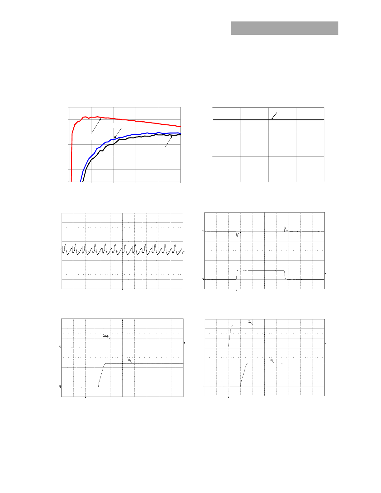
The following figures provide typical characteristics for the PNVX002A0X-SRZ (2.5V, 2A) at 25oC.
100
95
90
85
80
EFFICIENCY, η (%)
75
70
Vin=3.3V
0 0.4 0.8 1.2 1.6 2
Vin=12V
Vin=14V
OUTPUT CURRENT, IO (A) AMBIENT TEMPERATURE, TA OC
Figure 19. Converter Efficiency versus Output Current.
2.1
1.9
1.7
OUTPUT CURRENT, Io (A)
1.5
45 55 65 75 85
Figure 20. Derating Output Current versus Ambient
Temperature and Airflow.
Datasheet
NC
(V) (20mV/div)
O
V
OUTPUT VOLTAGE
TIME, t (2μs/div) TIME, t (500μs /div)
Figure 21. Typical output ripple and noise (V
o,max).
I
(V) (5V/div)
ON/PFF
(V) (1V/div) V
O
OUTPUT VOLTAGE ON/OFF VOLTAGE
V
TIME, t (5ms/div) TIME, t (5ms/div)
IN = 12V, Io =
(V) (100mV/div)
O
,
(A) (1Adiv) V
O
I
Figure 22. Transient Response to Dynamic Load Change
from 0% to 50% to 0%.
(V) (5V/div)
IN
(V) (1V/div) V
O
OUTPUT VOLTAGE INPUT VOLTAGE
V
Figure 23. Typical Start-up Using On/Off Voltage (Io = Io,max,
in=12V,Cext= 22uF ).
V
Figure 24. Typical Start-up Using Input Voltage (V
22 uF, Io = Io,max).
Cext=
IN = 12V,
June 24, 2013 ©2012 General Electric Company. All rights reserved. Page 9
Page 10
OUTPUT
CURRENT
OUTPUT
VOLTAGE
GE Energy
2A DLynxTM: Non-Isolated DC-DC Power Modules
3Vdc –14Vdc input; 0.6Vdc to 5.5Vdc output; 2A Output Current
Characteristic Curves
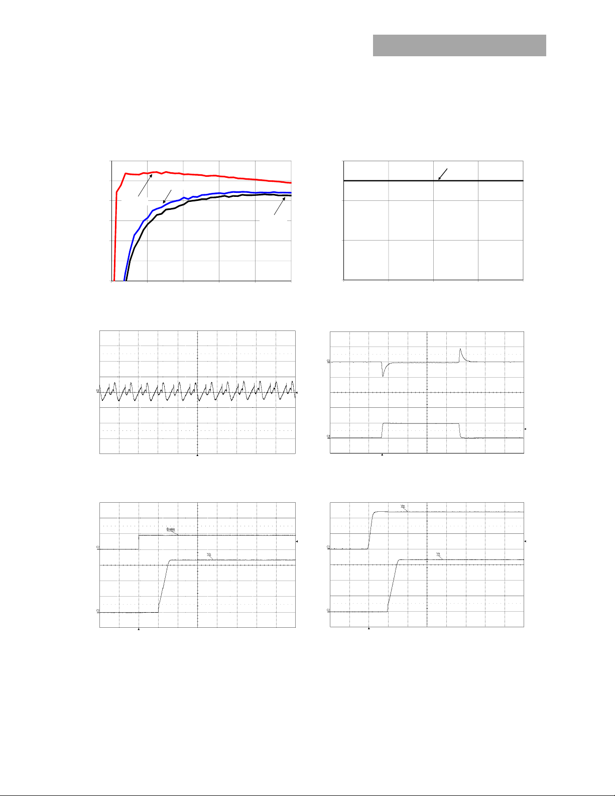
The following figures provide typical characteristics for the PNVX002A0X-SRZ (3.3V, 2A) at 25oC.
100
95
90
Vin=4.5V
85
80
EFFICIENCY, η (%)
75
70
0 0.4 0.8 1.2 1.6 2
Vin=12V
Vin=14V
OUTPUT CURRENT, IO (A) AMBIENT TEMPERATURE, TA OC
Figure 25. Converter Efficiency versus Output Current.
2.1
1.9
1.7
OUTPUT CURRENT, Io (A)
1.5
45 55 65 75 85
Figure 26. Derating Output Current versus Ambient
Temperature and Airflow.
Datasheet
NC
(V) (20mV/div)
O
V
OUTPUT VOLTAGE
TIME, t (1μs/div) TIME, t (500μs /div)
Figure 27. Typical output ripple and noise (V
o,max).
I
(V) (5V/div)
ON?OFF
(V) (1V/div) V
O
OUTPUT VOLTAGE ON/OFF VOLTAGE
V
TIME, t (5ms/div) TIME, t (5ms/div)
IN = 12V, Io =
(V) (100mV/div)
O
,
(A) (1Adiv) V
O
I
Figure 28. Transient Response to Dynamic Load Change
from 0% to 50% to 0%.
(V) (5V/div)
IN
(V) (1V/div) V
O
OUTPUT VOLTAGE INPUT VOLTAGE
V
Figure 29. Typical Start-up Using On/Off Voltage (Io = Io,max,
in=12V,Cext= 22uF)
V
Figure 30. Typical Start-up Using Input Voltage (V
22 uF, Io = Io,max).
Cext=
IN = 12V,
June 24, 2013 ©2012 General Electric Company. All rights reserved. Page 10
Page 11
OUTPUT
CURRENT
OUTPUT
VOLTAGE
GE Energy
2A DLynxTM: Non-Isolated DC-DC Power Modules
3Vdc –14Vdc input; 0.6Vdc to 5.5Vdc output; 2A Output Current
Characteristic Curves
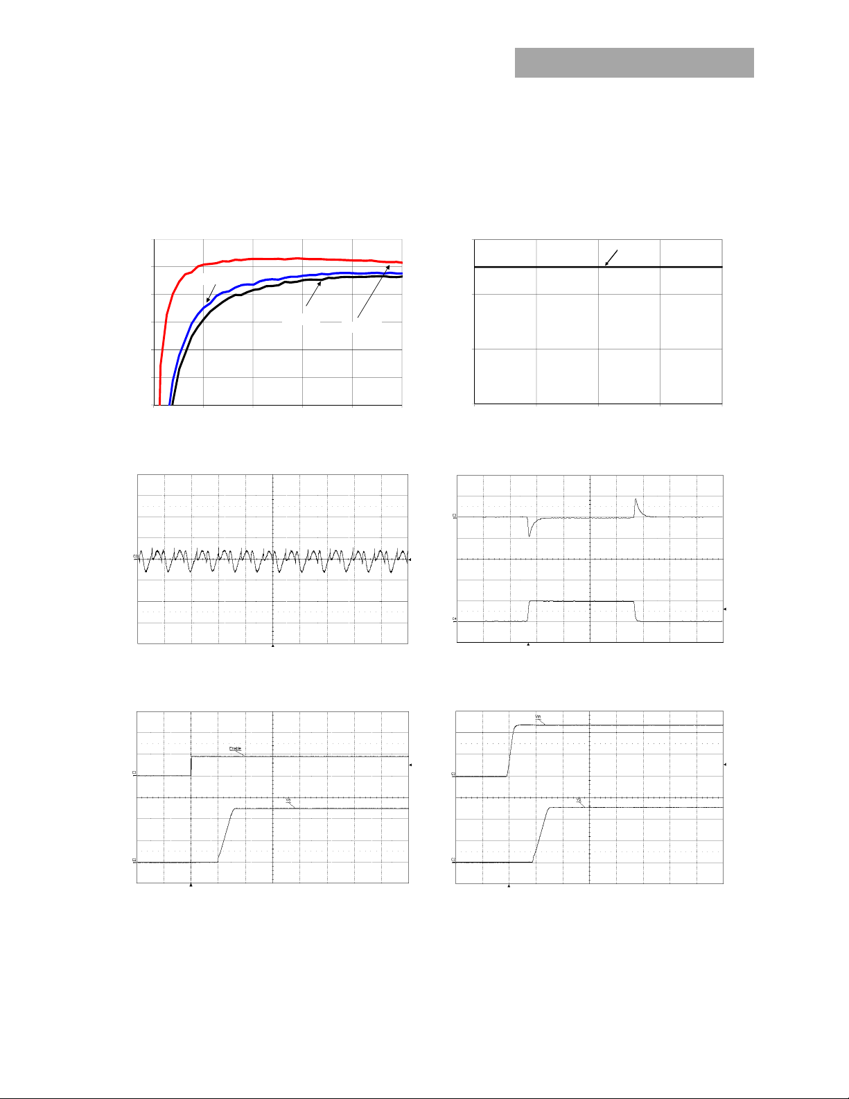
The following figures provide typical characteristics for the PNVX002A0X-SRZ (5V, 2A) at 25oC.
100
95
90
85
80
EFFICIENCY, η (%)
75
70
0 0.4 0.8 1.2 1.6 2
Vin=12V
Vin=14V
Vin=6.5V
OUTPUT CURRENT, IO (A) AMBIENT TEMPERATURE, TA OC
Figure 31. Converter Efficiency versus Output Current.
2.1
1.9
1.7
OUTPUT CURRENT, Io (A)
1.5
45 55 65 75 85
Figure 32. Derating Output Current versus Ambient
Temperature and Airflow.
Datasheet
NC
(V) (20mV/div)
O
V
OUTPUT VOLTAGE
TIME, t (2μs/div) TIME, t (500μs /div)
Figure 33. Typical output ripple and noise (V
o,max).
I
(V) (5V/div)
ON/OFF
(V) (2V/div) V
O
OUTPUT VOLTAG E ON/OFF VOLTAGE
V
TIME, t (5ms/div) TIME, t (5ms/div)
IN = 12V, Io =
(V) (100mV/div)
O
,
(A) (1Adiv) V
O
I
Figure 34. Transient Response to Dynamic Load Change
from 0% to 50% to 0%.
(V) (5V/div)
IN
OUTPUT VOLTAGE INPUT VOLTAGE
Vo (V) (2V/div) V
Figure 35. Typical Start-up Using On/Off Voltage (Io = Io,max,
Vin=12V,Cext= 22uF).
Figure 36. Typical Start-up Using Input Voltage (V
o = Io,max, Cext= 22uF).
I
IN = 12V,
June 24, 2013 ©2012 General Electric Company. All rights reserved. Page 11
Page 12
GE Energy
2A DLynxTM: Non-Isolated DC-DC Power Modules
3Vdc –14Vdc input; 0.6Vdc to 5.5Vdc output; 2A Output Current
Test Configurations
TO OSCILLOSCOPE
L
TEST
1μH
CS 1000μF
BATTERY
NOTE: Measure input reflected ripple current with a simulated
Electrolytic
E.S.R.<0.1Ω
@ 20°C 100kHz
source induc tance (L
possible battery impedance. Measure current as shown
above.
) of 1μH. Capacit or CS offsets
TEST
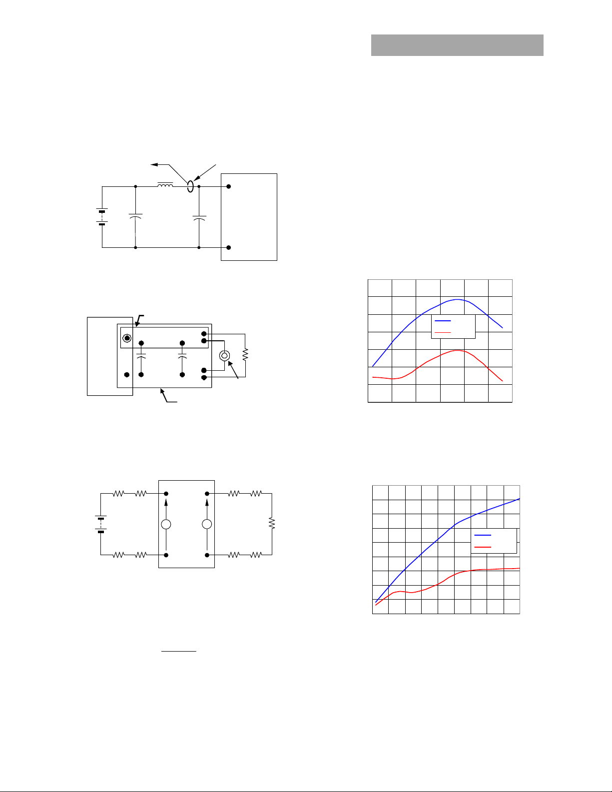
Figure 37. Input Reflected Ripple Current Test Setup.
COPPER STRIP
Vo+
0.1uF
COM
GROUND PLANE
NOTE : All volt age measurem ents to be t aken at the module
termin als, as shown ab ove. If soc kets are use d then
Kelvin connections are required at the module terminals
to av oid me asur ement er rors due to socket contac t
resistance.
Figure 38. Output Ripple and Noise Test Setup.
R
R
contact
distribution
R
R
contact
distribution
NOTE: All volt age meas urements to be taken at th e module
terminals , as shown above. If socket s are us ed then
Kelvin conn ections are requir ed at the modu le termi nals
to avoid measur ement err ors due to soc ket contact
resistance.
VIN(+)
V
IN
COM
Figure 39. Output Voltage and Efficiency Test Setup.
V
. I
O
Efficiency
=
η
VIN. I
O
IN
10uF
V
O
COM
2x100μF
Tantalum
CURRENT PROBE
CIN
SCO PE U SIN G
BNC SOC KET
R
contact Rdistribution
V
O
R
contact Rdistribution
x 100 %
VIN(+)
COM
RESISTIVE
LOAD
R
LOAD
Design Considerations
Input Filtering
The 12V DLynxTM 2A module should be connected to a
low ac-impedance source. A highly inductive source
can affect the stability of the module. An input
capacitance must be placed directly adjacent to the
input pin of the module, to minimize input ripple
voltage and ensure module stability.
To minimize input voltage ripple, ceramic capacitors
are recommended at the input of the module. Figure
40 shows the input ripple voltage for various output
voltages at 2A of load current with 1x10 µF or 1x22 µF
ceramic capacitors and an input of 5V. Figure 41
shows the input ripple voltage for an input of 12V
90
80
70
60
50
40
30
Input Ripple Voltage (mVp-p)
20
0.5 1 1.5 2 2.5 3 3.5
Output Voltage (Vdc)
Figure 40. Input ripple voltage for various output
voltages with 1x10 µF or 1x22 µF ceramic capacitors
at the input (2A load). Input voltage is 5V. Scope BW:
20MHz.
110
100
90
80
70
60
50
40
30
Input Ripple Voltage (mVp-p)
20
0.5 1 1.5 2 2.5 3 3 .5 4 4.5 5
Output Voltage (Vdc)
Figure 41. Input ripple voltage for various output
voltages with 1x10 µF or 1x22 µF ceramic capacitors
at the input (2A load). Input voltage is 12V. Scope BW:
20MHz
Datasheet
1x10uF
1x22uF
1x10uF
1x22uF
June 24, 2013 ©2012 General Electric Company. All rights reserved. Page 12
Page 13
GE Energy
2A DLynxTM: Non-Isolated DC-DC Power Modules
3Vdc –14Vdc input; 0.6Vdc to 5.5Vdc output; 2A Output Current
Output Filtering
The 12V DLynxTM 2A modules are designed for low output ripple
voltage and will meet the maximum output ripple specification
with 0.1 µF ceramic and 22µF ceramic capacitors at the output
of the module. However, additional output filtering may be
required by the system designer for a number of reasons. First,
there may be a need to further reduce the output ripple and
noise of the module. Second, the dynamic response
characteristics may need to be customized to a particular load
step change.
To reduce the output ripple and improve the dynamic response
to a step load change, additional capacitance at the output can
be used. Low ESR polymer and ceramic capacitors are
recommended to improve the dynamic response of the
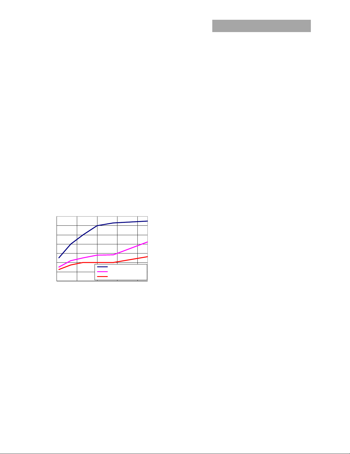
module. A minimum 22uF External Cap must be used. Figure
42 provides output ripple information for different external
capacitance values at various Vo and for a load current of 2A.
For stable operation of the module, limit the capacitance to less
than the maximum output capacitance as specified in the
electrical specification table. Optimal performance of the
module can be achieved by using the Tunable Loop
described later in this data sheet.
TM
feature
The input to these units is to be provided with a slowblow fuse with a maximum rating of 4A in the positive
input lead
.
Datasheet
14
12
10
8
6
Ripple(m Vp-p)
4
2
0
0.51.52.53.54.5
Output Voltage(Volts)
Figure 42. Output ripple voltage for various output voltages
with external 1x22 µF, 1x47 µF or 2x47 µF ceramic capacitors
at the output (2A load). Input voltage is 12V.
1x22uF External Cap
1x47uF External Cap
2x47uF External cap
Safety Considerations
For safety agency approval the power module must be
installed in compliance with the spacing and separation
requirements of the end-use safety agency standards, i.e., UL
60950-1 2nd, CSA C22.2 No. 60950-1-07, DIN EN 60950-1:2006
+ A11 (VDE0805 Teil 1 + A11):2009-11; EN 60950-1:2006 +
A11:2009-03.
For the converter output to be considered meeting the
requirements of safety extra-low voltage (SELV), the input must
meet SELV requirements. The power module has extra-low
voltage (ELV) outputs when all inputs are ELV.
June 24, 2013 ©2012 General Electric Company. All rights reserved. Page 13
Page 14
GE Energy
2A DLynxTM: Non-Isolated DC-DC Power Modules
3Vdc –14Vdc input; 0.6Vdc to 5.5Vdc output; 2A Output Current
Feature Descriptions
Remote Enable
The 12V DLynxTM 2A power modules feature an On/Off pin for
remote On/Off operation. Two On/Off logic options are
available. In the Positive Logic On/Off option, (device code
suffix “4” – see Ordering Information), the module turns ON
during a logic High on the On/Off pin and turns OFF during a
logic Low. With the Negative Logic On/Off option, (no device
code suffix, see Ordering Information), the module turns OFF
during logic High and ON during logic Low. The On/Off signal is
always referenced to ground. For either On/Off logic option,
leaving the On/Off pin disconnected will turn the module ON
when input voltage is present.
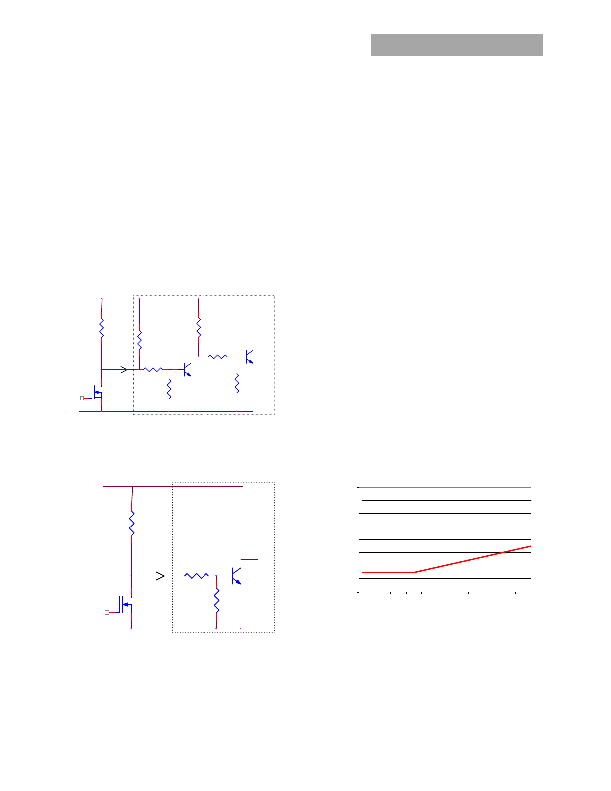
For positive logic modules, the circuit configuration for using
the On/Off pin is shown in Figure 43. Contact GE Energy
regarding availability of positive logic module
VIN+
Rpullup
I
GND
ON/OFF
V
ON/OFF
Q1
+
_
ON/O FF
Figure 43. Circuit configuration for using positive On/Off
logic.
For negative logic On/Off modules, the circuit configuration is
shown in Fig. 44.
MOD UL E
50K
10K
10K
50K
PWM Enable
10K
Q2
Q3
10K
Overcurrent Protection
To provide protection in a fault (output overload)
condition, the unit is equipped with internal
current-limiting circuitry and can endure current limiting
continuously. At the point of current-limit inception, the
unit enters hiccup mode. The unit operates normally
once the output current is brought back into its specified
range.
Overtemperature Protection
To provide protection in a fault condition, the unit is
equipped with a thermal shutdown circuit. The unit will
shutdown if the overtemperature threshold of 140
exceeded at the thermal reference point T
thermal shutdown is not intended as a guarantee that
the unit will survive temperatures beyond its rating.
Once the unit goes into thermal shutdown it will then
wait to cool before attempting to restart.
Input Undervoltage Lockout
At input voltages below the input undervoltage lockout
limit, the module operation is disabled. The module will
begin to operate at an input voltage above the
undervoltage lockout turn-on threshold.
Output Voltage Programming
The output voltage of the 12V DLynxTM 2A modules can
be programmed to any voltage from 0.6dc to 5.5Vdc by
connecting a resistor between the Trim and GND pins of
the module. Certain restrictions apply on the output
voltage set point depending on the input voltage. These
are shown in the Output Voltage vs. Input Voltage Set
Point Area plot in Fig. 45. The Lower Limit curve shows
that for output voltages of 2.4V and higher, the input
voltage needs to be larger than the minimum of 3V.
Datasheet
ref
. The
o
C is
VIN +
ON/OFF
GND
Rpullup
I
ON/OFF
+
V
ON/OFF
Q1
_
MODULE
PWM Enable
Q2
10K
10K
Figure 44. Circuit configuration for using negative On/Off
logic.
16
14
12
10
8
6
Input Voltage (v)
4
2
0
0.5 1 1.5 2 2.5 3 3.5 4 4.5 5 5.5 6
Output Voltage (V)
Figure 45. Output Voltage vs. Input Voltage Set Point
Area plot showing limits where the output voltage can
be set for different input voltages.
Without an external resistor between Trim and GND pins,
the output of the module will be 0.6Vdc. To calculate the
value of the trim resistor, Rtrim for a desired output
voltage, use the following equation:
June 24, 2013 ©2012 General Electric Company. All rights reserved. Page 14
Page 15
GE Energy
2A DLynxTM: Non-Isolated DC-DC Power Modules
3Vdc –14Vdc input; 0.6Vdc to 5.5Vdc output; 2A Output Current
Rtrim
Rtrim is the external resistor in kΩ
Vo is the desired output voltage.
Table 1 provides Rtrim values required for some common
output voltages.
()
Vo
= k
0.6
−
Ω
6.0
Table 1
V
(V) Rtrim (KΩ)
O, set
1.0 15
1.2 10
1.5 6.67
1.8 5
2.5 3.16
3.3 2.22
5.0 1.36
By using a ±0.5% tolerance trim resistor with a TC of ±100ppm,
a set point tolerance of ±1.5% can be achieved as specified in
the electrical specification.
Please consult your local GE Energy technical
representative for additional details.
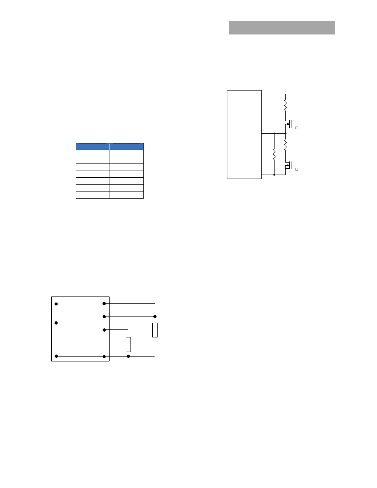
Figure 47. Circuit Configuration for margining Output
voltage.
MODULE
Datasheet
Vo
Rmargin-down
Q2
Trim
Rmargin-up
Rtrim
Q1
GND
Remote Sense
The 12V DLynxTM 2A power modules have a Remote Sense
feature to minimize the effects of distribution losses by
regulating the voltage at the SENSE pin. The voltage between
the SENSE pin and VOUT pin must not exceed 0.5V. Note that
the output voltage of the module cannot exceed the specified
maximum value. This includes the voltage drop between the
SENSE and Vout pins. When the Remote Sense feature is not
being used, connect the SENSE pin to the VOUT pin.
GND
VO(+)
SEN SE
TRIM
LOA D
R
tri m
VIN(+)
ON/OFF
Figure 46. Circuit configuration for programming output
voltage using an external resistor.
Voltage Margining
Output voltage margining can be implemented in the 12V
TM
2A modules by connecting a resistor, R
DLynx
the Trim pin to the ground pin for margining-up the output
voltage and by connecting a resistor, R
pin to output pin for margining-down. Figure 10 shows the
circuit configuration for output voltage margining. The POL
Programming Tool, available at www.lineagepower.com under
the Design Tools section, also calculates the values of R
and R
margin-down
for a specific output voltage and % margin.
margin-down
, from
margin-up
, from the Trim
margin-up
June 24, 2013 ©2012 General Electric Company. All rights reserved. Page 15
Page 16
V
V
V
GE Energy
2A DLynxTM: Non-Isolated DC-DC Power Modules
3Vdc –14Vdc input; 0.6Vdc to 5.5Vdc output; 2A Output Current
Monotonic Start-up and Shutdown
The 12V DLynx
shutdown behavior for any combination of rated input voltage,
output current and operating temperature range.
TM
2A modules have monotonic start-up and
Startup into Pre-biased Output
The 12V DLynxTM 2A modules can start into a prebiased output
as long as the prebias voltage is 0.5V less than the set output
voltage.
Power Good
The 12V DLynx
signal that is implemented with an open-drain output to
indicate that the output voltage is within the regulation limits of
the power module. The PGOOD signal will be de-asserted to a
low state if any condition such as overtemperature, overcurrent
or loss of regulation occurs that would result in the output
voltage going ±12.5% outside the setpoint value. The PGOOD
terminal should be connected through a pullup resistor
(suggested value 100KΩ) to a source of 5VDC or lower.
Tunable Loop
The 12V DLynxTM 2A modules have a new feature that
optimizes transient response of the module called Tunable
TM
Loop
External capacitors are usually added to the output of the
module for two reasons: to reduce output ripple and noise (see
Fig. 42) and to reduce output voltage deviations from the
steady-state value in the presence of dynamic load current
changes. Adding external capacitance however affects the
voltage control loop of the module, typically causing the loop to
slow down with sluggish response. Larger values of external
capacitance could also cause the module to become unstable.
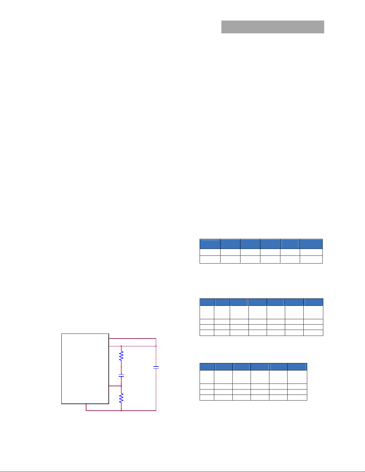
The Tunable Loop
voltage control loop to match the filter network connected to
the output of the module. The Tunable Loop
by connecting a series R-C between the SENSE and TRIM pins of
the module, as shown in Fig. 48. This R-C allows the user to
externally adjust the voltage loop feedback compensation of
the module.
TM
2A modules provide a Power Good (PGOOD)
TM
.
TM
allows the user to externally adjust the
TM
is implemented
VOUT
SENSE
RTUNE
MODULE
C O
CTUNE
TRIM
GND
Figure. 48. Circuit diagram showing connection of R
to tune the control loop of the module.
C
TUNE
RTrim
TUME
and
Recommended values of R
output capacitor combinations are given in Tables 2 and
3. Table 2 shows the recommended values of R
for different values of ceramic output capacitors up
C
TUNE
to 470uF that might be needed for an application to
meet output ripple and noise requirements. Selecting
and C
R
TUNE
TUNE
operation of the module.
In applications with tight output voltage limits in the
presence of dynamic current loading, additional output
capacitance will be required. Tables 3,4 and 5 list
recommended values of R
2% output voltage deviation limits for some common
output voltages in the presence of a 1A to 2A step
change (50% of full load), for input voltages of 12V, 5V
and 3.3V respectively.
Please contact your GE Energy technical representative
to obtain more details of this feature as well as for
guidelines on how to select the right value of external RC to tune the module for best transient performance and
stable operation for other output capacitance values or
input voltages other than 12V.
Table 2. General recommended values of of R
for Vin=12V/5V/3.3V and various external
C
TUNE
ceramic capacitor combinations.
Co
1x47μF 2x47μF 3x47μF 4x47μF 10x47μF
R
TUNE
C
3900pF 10nF 18nF 18nF 22nF
TUNE
Table 3. Recommended values of R
obtain transient deviation of ≤2% of Vout for a 1A step
load with Vin=12V
o 5V 3.3V 2.5V 1.8V 1.2V 0.6
Co
1x22μF1x47μF2x47μF 2x47μF 3x47μF
R
220 220 150 150 100 100
TUNE
C
2200pF 3900pF 10nF 10nF 18nF 68nF
TUNE
81mV 61mV 35mV 34mV 23mV 12mV
ΔV
Table 4. Recommended values of R
obtain transient deviation of ≤2% of Vout for a 1A step
load with Vin=5V
o 3.3V 2.5V 1.8V 1.2V 0.6V
Co
1x47μF2x47μF2x47μF 3x47μF
R
220 150 150 100 100
TUNE
C
3900pF 10nF 10nF 18nF 68nF
TUNE
62mV 35mV 34mV 23mV 12mV
ΔV
Datasheet
and C
TUNE
according to Table 2 will ensure stable
and C
TUNE
220 150 100 100 100
for different
TUNE
in order to meet
TUNE
TUNE
and C
TUNE
TUNE
and C
330μF
Polymer
TUNE
TUNE
TUNE
and
and
to
330μF
Polymer
to
June 24, 2013 ©2012 General Electric Company. All rights reserved. Page 16
Page 17
GE Energy
2A DLynxTM: Non-Isolated DC-DC Power Modules
3Vdc –14Vdc input; 0.6Vdc to 5.5Vdc output; 2A Output Current
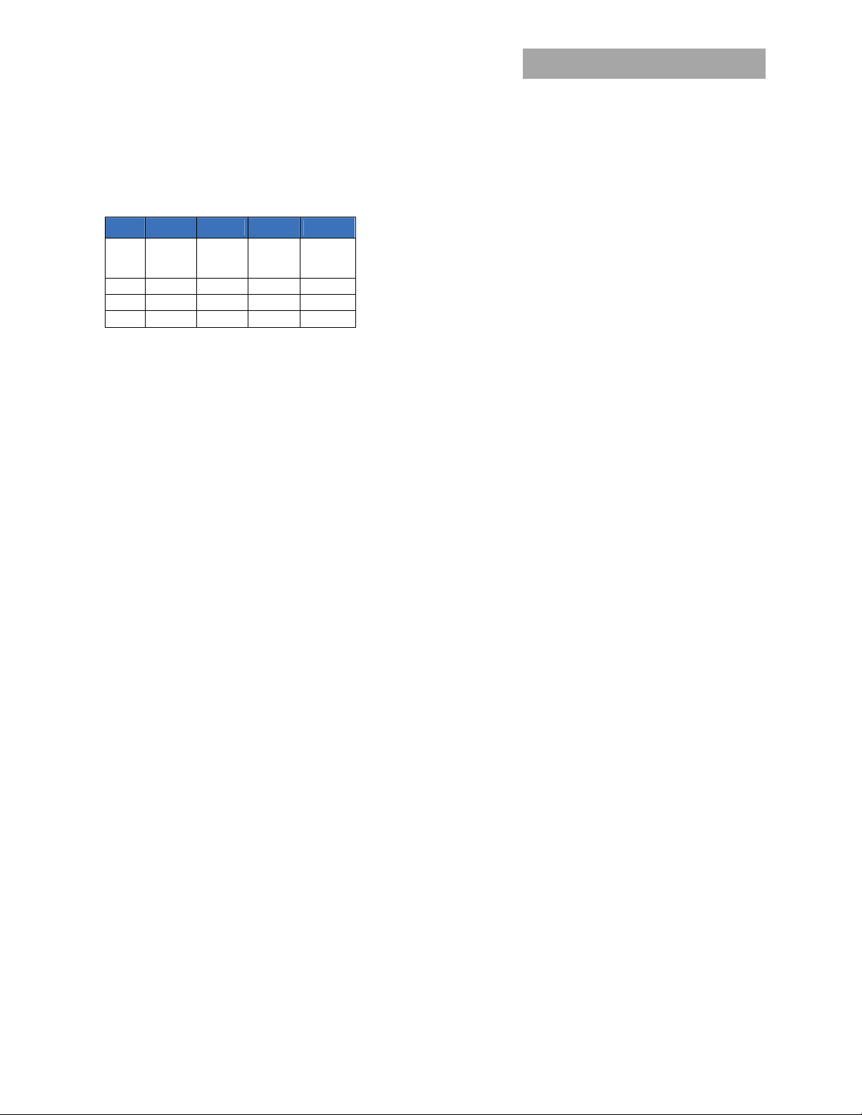
Table 5. Recommended values of R
transient deviation of ≤2% of Vout for a 1A step load with
Vin=3.3V
Vo 2.5V 1.8V 1.2V 0.6V
Co
3x47μF 2x47μF 3x47μF
R
C
ΔV
100 150 100 100
TUNE
18nF 10nF 18nF 68nF
TUNE
48mV 34mV 23mV 12mV
TUNE
and C
330μF
Polymer
TUNE
to obtain
Datasheet
June 24, 2013 ©2012 General Electric Company. All rights reserved. Page 17
Page 18
Air
GE Energy
2A DLynxTM: Non-Isolated DC-DC Power Modules
3Vdc –14Vdc input; 0.6Vdc to 5.5Vdc output; 2A Output Current
Thermal Considerations
Power modules operate in a variety of thermal environments;
however, sufficient cooling should always be provided to help
ensure reliable operation.
Considerations include ambient temperature, airflow, module
power dissipation, and the need for increased reliability. A
reduction in the operating temperature of the module will result
in an increase in reliability. The thermal data presented here is
based on physical measurements taken in a wind tunnel. The
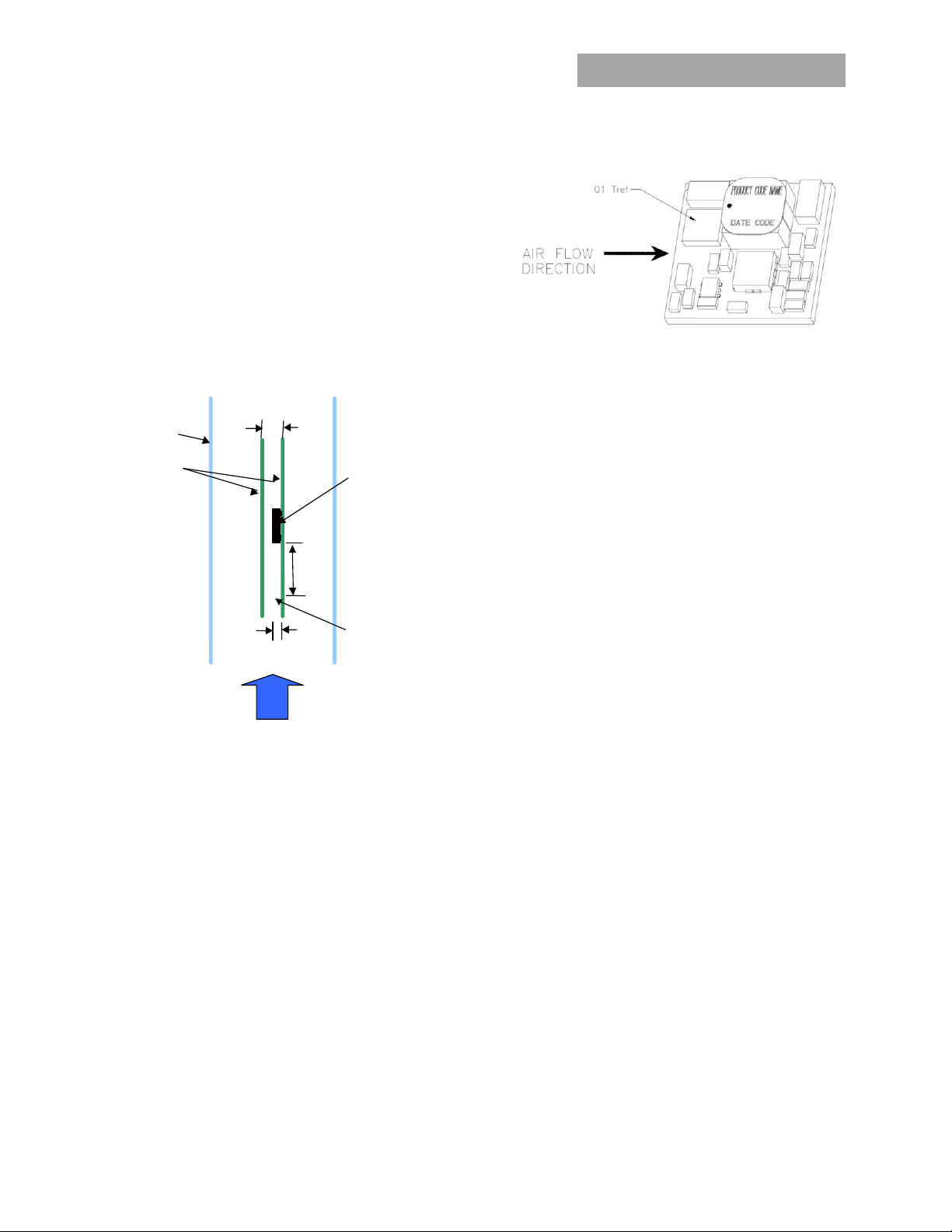
test set-up is shown in Figure 49. The preferred airflow
direction for the module is in Figure 50.
25.4_
ind Tunnel
PWBs
(1.0)
Power Module
Figure 50. Preferred airflow direction and location of
hot-spot of the module (Tref).
Datasheet
76.2_
(3.0)
x
Probe Location
12.7_
(0.50)
for measuring
airflow and
ambient
temperature
flow
Figure 49. Thermal Test Setup.
The thermal reference points, T
also shown in Figure 50. For reliable operation the
temperatures at these points should not exceed 125
output power of the module should not exceed the rated power
of the module (Vo,set x Io,max).
Please refer to the Application Note “Thermal Characterization
Process For Open-Frame Board-Mounted Power Modules” for a
detailed discussion of thermal aspects including maximum
device temperatures.
used in the specifications are
ref
o
C. The
June 24, 2013 ©2012 General Electric Company. All rights reserved. Page 18
Page 19
GE Energy
2A DLynxTM: Non-Isolated DC-DC Power Modules
3Vdc –14Vdc input; 0.6Vdc to 5.5Vdc output; 2A Output Current
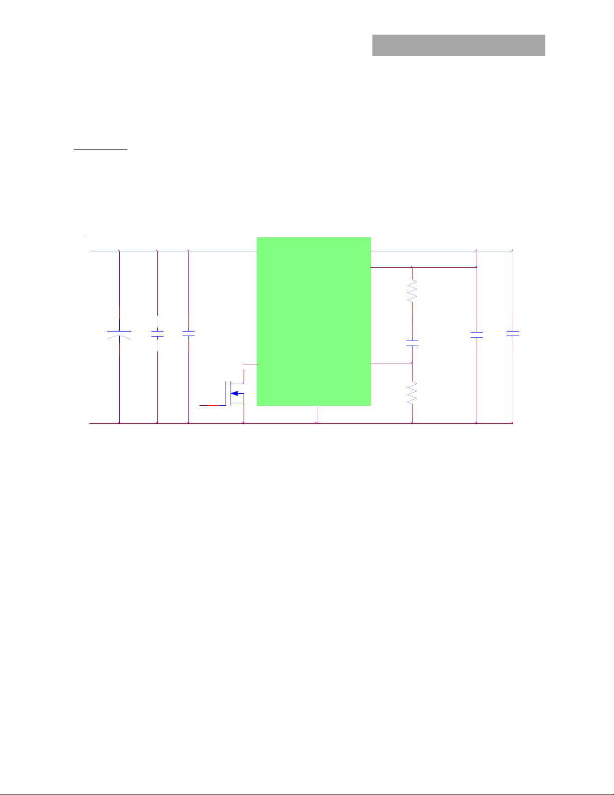
Example Application Circuit
Requirements:
Vin: 12V
Vout: 1.8V
Iout: 1A max., worst case load transient is from 1A to 1.5A
ΔVout: 1.5% of Vout (27mV) for worst case load transient
Vin, ripple 1.5% of Vin (180mV, p-p)
Vin+
VIN
+
CI3
CI2
CI1
MODULE
VOUT
SENSE
Datasheet
RTUNE
CTUNE
Vout+
CO1
CO2
Q3
ON/OFF
GND
CI1 1x0.1μF/16V ceramic capacitor (0402 size)
CI2 1x10μF/16V ceramic capacitor (e.g. TDK C Series)
CI2 100μF/16V bulk electrolytic
CO1 1x0.1μF/16V ceramic capacitor (0402 size)
CO1 2x47μF/6.3V ceramic capacitor (e.g. TDK C Series, Murata GRM32ER60J476ME20)
CTune 5600pF ceramic capacitor
RTune 150 ohms SMT resistor
RTrim 5kΩ SMT resistor (recommended tolerance of 0.1%)
TRIM
RTrim
June 24, 2013 ©2012 General Electric Company. All rights reserved. Page 19
Page 20
GE Energy
2A DLynxTM: Non-Isolated DC-DC Power Modules
3Vdc –14Vdc input; 0.6Vdc to 5.5Vdc output; 2A Output Current
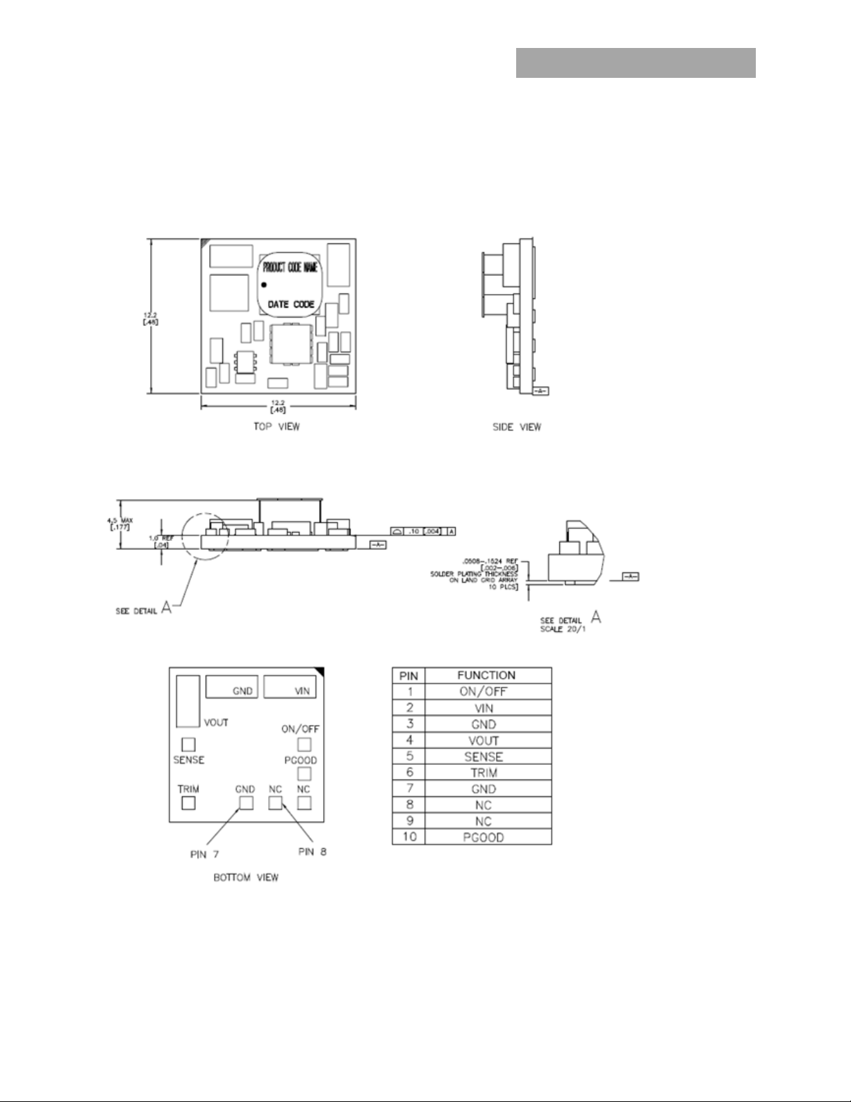
Mechanical Outline
Dimensions are in millimeters and (inches).
Tolerances: x.x mm ± 0.5 mm (x.xx in. ± 0.02 in.) [unless otherwise indicated]
x.xx mm ± 0.25 mm (x.xxx in ± 0.010 in.)
Datasheet
June 24, 2013 ©2012 General Electric Company. All rights reserved. Page 20
Page 21
GE Energy
2A DLynxTM: Non-Isolated DC-DC Power Modules
3Vdc –14Vdc input; 0.6Vdc to 5.5Vdc output; 2A Output Current
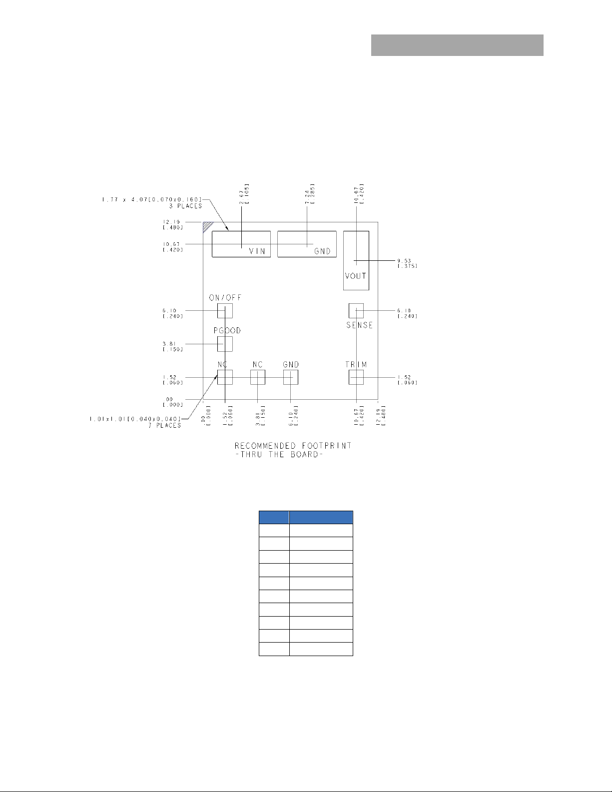
Recommended Pad Layout
Dimensions are in millimeters and (inches).
Tolerances: x.x mm ± 0.5 mm (x.xx in. ± 0.02 in.) [unless otherwise indicated]
x.xx mm ± 0.25 mm (x.xxx in ± 0.010 in.)
Datasheet
June 24, 2013 ©2012 General Electric Company. All rights reserved. Page 21
PIN FUNCTION
1 ON/OFF
2 VIN
3 GND
4 VOUT
5 SENSE
6 TRIM
7 GND
8 NC
9 NC
10 PGOOD
Page 22
GE Energy
Datasheet
2A DLynxTM: Non-Isolated DC-DC Power Modules
3Vdc –14Vdc input; 0.6Vdc to 5.5Vdc output; 2A Output Current
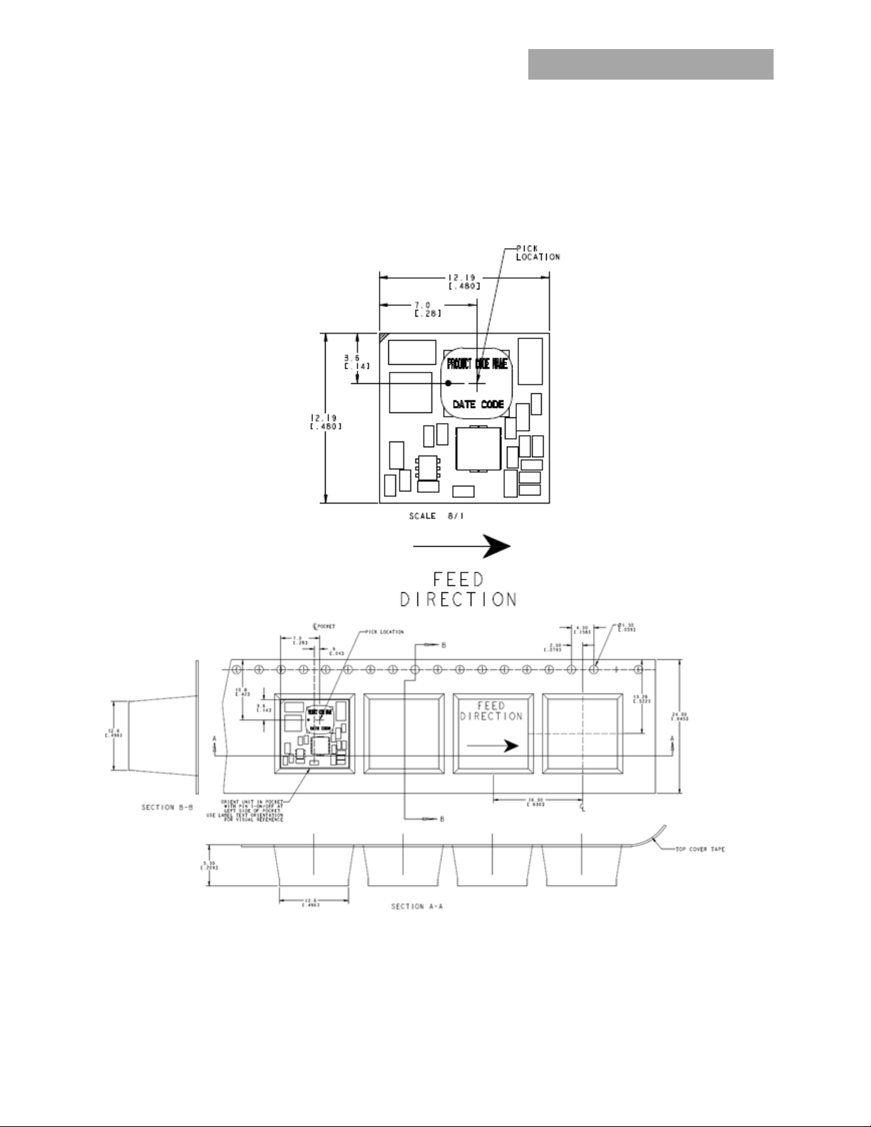
Packaging Details
The 12V DLynxTM 2A modules are supplied in tape & reel as standard. Modules are shipped in quantities of 400 modules per reel.
All Dimensions are in millimeters and (in inches).
Reel Dimensions:
Outside Dimensions: 330.2 mm (13.00)
Inside Dimensions: 177.8 mm (7.00”)
Tape Width: 24.00 mm (0.945”)
June 24, 2013 ©2012 General Electric Company. All rights reserved. Page 22
Page 23
GE Energy
2A DLynxTM: Non-Isolated DC-DC Power Modules
3Vdc –14Vdc input; 0.6Vdc to 5.5Vdc output; 2A Output Current
Surface Mount Information
Pick and Place
The 12V DLynxTM 2A modules use an open frame construction
and are designed for a fully automated assembly process. The
modules are fitted with a label designed to provide a large
surface area for pick and place operations. The label meets all
the requirements for surface mount processing, as well as
safety standards, and is able to withstand reflow temperatures
of up to 300
as product code, serial number and the location of
manufacture.
Nozzle Recommendations
The module weight has been kept to a minimum by using open
frame construction. Variables such as nozzle size, tip style,
vacuum pressure and placement speed should be considered
to optimize this process. The minimum recommended inside
nozzle diameter for reliable operation is 3mm. The maximum
nozzle outer diameter, which will safely fit within the allowable
component spacing, is 7 mm.
Bottom Side / First Side Assembly
This module is not recommended for assembly on the bottom
side of a customer board. If such an assembly is attempted,
components may fall off the module during the second reflow
process. If assembly on the bottom side is planned, please
contact GE Energy for special manufacturing process
instructions.
Only ruggedized (-D version) modules with additional epoxy will
work with a customer’s first side assembly. For other versions,
first side assembly should be avoided
o
C. The label also carries product information such
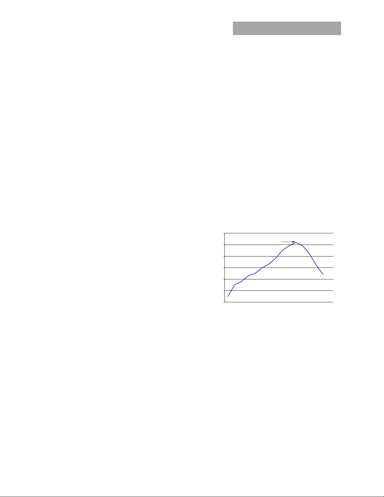
The recommended linear reflow profile using Sn/Ag/Cu
solder is shown in Fig. 51. Soldering outside of the
recommended profile requires testing to verify results
and performance.
MSL Rating
The 12V DLynxTM 2A modules have a MSL rating of 2a.
Storage and Handling
The recommended storage environment and handling
procedures for moisture-sensitive surface mount
packages is detailed in J-STD-033 Rev. A (Handling,
Packing, Shipping and Use of Moisture/Reflow Sensitive
Surface Mount Devices). Moisture barrier bags (MBB)
with desiccant are required for MSL ratings of 2 or
greater. These sealed packages should not be broken
until time of use. Once the original package is broken,
the floor life of the product at conditions of ≤ 30°C and
60% relative humidity varies according to the MSL rating
(see J-STD-033A). The shelf life for dry packed SMT
packages will be a minimum of 12 months from the bag
seal date, when stored at the following conditions: < 40°
C, < 90% relative humidity.
300
Per J-STD-020 Rev. C
250
200
150
Heating Zone
1°C/Second
100
Reflow Temp (°C)
50
Datasheet
Peak Temp 260°C
* Min. Time Above 235°C
15 Seconds
*Time Above 217°C
60 S econds
Cooling
Zone
Lead Free Soldering
The 12V DLynxTM 2A modules are lead-free (Pb-free) and RoHS
compliant and fully compatible in a Pb-free soldering process.
Failure to observe the instructions below may result in the
failure of or cause damage to the modules and can adversely
affect long-term reliability.
0
Reflow Time (Seconds)
Figure 51. Recommended linear reflow profile using
Sn/Ag/Cu solder.
Post Solder Cleaning and Drying Considerations
Post solder cleaning is usually the final circuit-board
Pb-free Reflow Profile
Power Systems will comply with J-STD-020 Rev. C
(Moisture/Reflow Sensitivity Classification for
Nonhermetic Solid State Surface Mount Devices) for both
Pb-free solder profiles and MSL classification procedures.
This standard provides a recommended forced-airconvection reflow profile based on the volume and
assembly process prior to electrical board testing. The
result of inadequate cleaning and drying can affect both
the reliability of a power module and the testability of the
finished circuit-board assembly. For guidance on
appropriate soldering, cleaning and drying procedures,
refer to Board Mounted Power Modules: Soldering and
Cleaning Application Note (AN04-001).
thickness of the package (table 4-2). The suggested Pbfree solder paste is Sn/Ag/Cu (SAC).
recommended.
For questions regarding Land grid array(LGA) soldering, solder
volume; please contact GE Energy for special manufacturing
process instructions.
June 24, 2013 ©2012 General Electric Company. All rights reserved. Page 23
A 6 mil thick stencil is
Page 24
GE Energy
Datasheet
2A DLynxTM: Non-Isolated DC-DC Power Modules
3Vdc –14Vdc input; 0.6Vdc to 5.5Vdc output; 2A Output Current
Ordering Information
Please contact your GE Energy Sales Representative for pricing, availability and optional features.
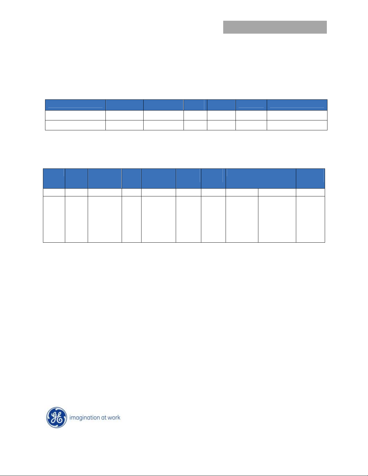
Table 6. Device Codes
Device Code
PNVX002A0X3-SRZ 3 – 14Vdc 0.6 – 5.5 Vdc 2A Negative No 150025978
PNVX002A0X3-SRDZ* 3 – 14Vdc 0.6 – 5.5 Vdc 2A Negative No TBD
-Z refers to RoHS compliant parts
* Check availability with GE Sales
Table 7. Coding Scheme
Package Family. Sequencing Output
P NV X 002A0 X 4 3 -SR -D* Z
P : Pico
U : Micro
M : Mega
G : Giga
A : Pre-
4G
NV:
DLynx
analog
open
frame.
T: with EZ-
SEQUENCE
X: without EZ-
SEQUENCE
Input
Voltage Range
current
2.0A X =
Output
Voltage
Output
voltage
programmable
output
Output
Current
On/Off
logic
4 =
positive
No entry =
negative
On/Off
Logic
Remote
Sense
3 =
Remote
Sense
No entry
=
negative
Sequencing Comcodes
Options ROHS
S = Surface
Mount
R =
Tape&Reel
D = 105C
operating
ambient, 40G
operating
shock as per
MIL Std 810F
Compliance
Z = ROHS6
Contact Us
For more information, call us at
USA/Canada:
+1 888 546 3243, or +1 972 244
9288
Asia-Pacific:
+86.021.54279977*808
Europe, Middle-East and Africa:
+49.89.878067-280
India:
+91.80.28411633
June 24, 2013 ©2012 General Electric Company. All rights reserved. Version 1.1
www.ge.com/powerelectronics
 Loading...