GS-EVB-HB-66508B-RN Technical Manual
DANGER!
handling the product.
_____________________________________________________________________________________________________________________
GS-EVB-HB-66508B-RN
Technical Manual
Visit www.gansystems.com
for the latest version of this technical manual.
This evaluation kit is designed for engineering evaluation in a controlled
lab environment and should be handled by qualified personnel ONLY.
High voltage will be exposed on the board during the test and even brief
contact during operation may result in severe injury or death.
Never leave the board operating unattended. After it is de-energized,
always wait until all capacitors are discharged before touching the board.
CAUTION:
This product contains parts that are susceptible to damage by electrostatic
discharge (ESD). Always follow ESD prevention procedures when
GS-EVB-HB-66508B-RN Rev. 210118 © 2021 GaN Systems Inc. www.gansystems.com 1
Please refer to the Evaluation Board/Kit Important Notice on page 26

GS-EVB-HB-66508B-RN Technical Manual
Part Number
GaN E-HEMT P/N:
Description
RAA226110 gate driver, 0V turn off voltage
GS665MB-EVB
Universal 650V Mother Board
_____________________________________________________________________________________________________________________
Overview
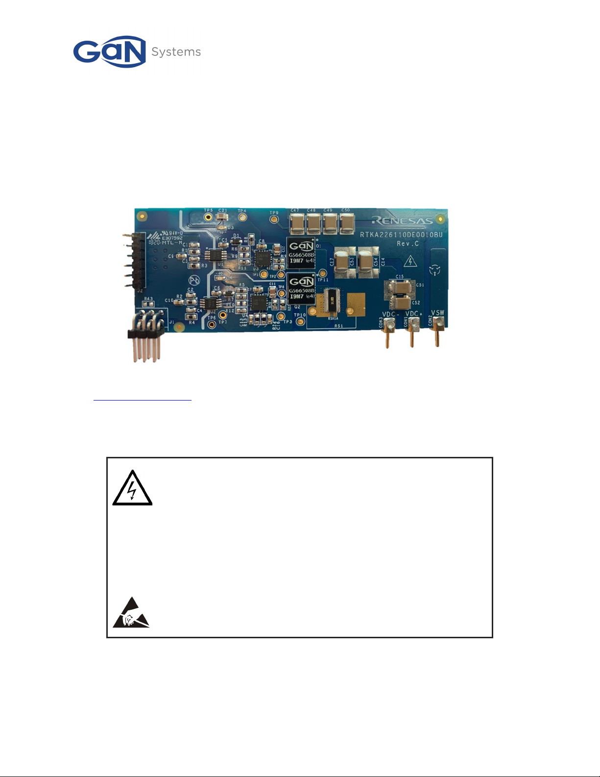
The GS-EVB-HB-66508B-RN is a RTK226110DE0010BU RAA226110
https://www.renesas.com/products/raa226110
daughter board style. This evaluation kit consists of two GaN Systems 650V GaN Enhancement-mode
HEMTs (E-HEMTs) and all necessary circuits including half bridge gate drivers, isolated power supplies
and optional heatsink to form a functional half bridge power stage. It allows users to easily evaluate the
GaN E-HEMT performance in any half bridge-based topology, either with the universal mother board
(P/N: GS665MB-EVB) or users’ own system design. The GS-EVB-HB-66508B-RN demo board provides 0V
turn-off voltage solution. 0V turn-off solution is normally used in low power application. 0V turn-off
solution is easy to implement as there is no need a negative power supply rail. And the reverse
conduction voltage drop of GaN is lower. For E-mode GaN device the Vgs threshold voltage is low (typ:
1.7V). 0V turn-off has the risk of false turn-on when the GaN device is in off state. Also, the switching-off
loss will be higher than negative turn-off voltage. The 0V turn-off solution is normally used in the low
power applications.
Features:
• Serves as a reference design and evaluation tool as well as deployment-ready solution for easy in-
system evaluation.
• Vertical mount style with height of 35mm, which fits in majority of 1U design and allows
evaluation of GaN E-HEMT in traditional through-hole type power supply board.
• Current shunt position for switching characterization testing
• Universal form factor and footprint for all products
• 0V turn off voltage
The daughter board and universal mother board ordering part numbers are below:
gate drive demo board following GS665XXX-EVBDB
Table 1 Ordering part numbers
GS-EVB-HB-66508B-RN GS66508B
GaN E-HEMT 650V/30A, 50mΩ With
Control and Power I/Os:
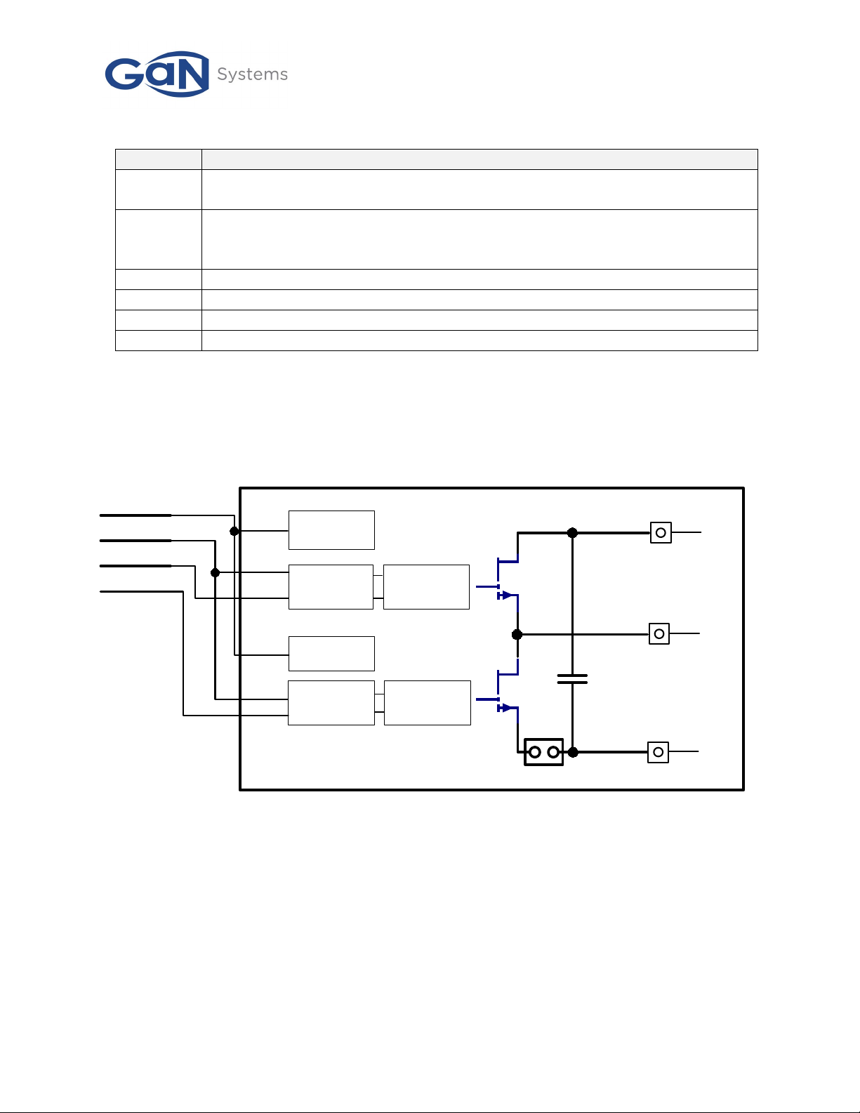
The daughter board GS-EVB-HB-66508B-RN circuit diagram is shown in Figure 1. The control logic
inputs on 2x3 pin header J1 are listed below:
GS-EVB-HB-66508B-RN Rev. 210118 © 2021 GaN Systems Inc. www.gansystems.com 2
Please refer to the Evaluation Board/Kit Important Notice on page 26
GS-EVB-HB-66508B-RN Technical Manual
Pin
Descriptipon
drive outputs.
switches.
VDRV
Not used. VDRV can be connected to VCC though R43. R43 is DNP by default.
PWMH_IN
High side PWM logic input for top switch Q1. It is compatible wth 3.3V and 5V
PWML_IN
Low side PWM logic input for bottom switch Q2. It is compatible wth 3.3V and 5V
0V
Logic inputs and gate drive power supply ground return.
IL611-1E
Q 1 Q
2
Iso
.
DC / DC
Iso
.
DC / DC
VDC
+
VSW
VDC
-
VCC
ENABLE
shunt
C 4 -
10
PWMH
PWML
Gate Driver
RAA226110
Gate Driver
IL611-1E
RAA226110
_____________________________________________________________________________________________________________________
Table 2 Control pins
ENABLE Enable input. It is internally pulled up to VCC, a low logic disables all the PWM gate
+5V +5V auxillary power supply input for logic circuit and gate driver. On the daughter
board there are 2 isolated 5V to 9V DC/DC power supplies for top and bottom
The 3 power pins are:
• VDC+: Input DC Bus voltage
• VSW: Switching node output
• VDC-: Input DC bus voltage ground return. Note that control ground 0V is isolated from VDC-
Isolator
Isolator
Figure 1 GS-EVB-HB-66508B-RN Evaluation Board Block Diagram
GS-EVB-HB-66508B-RN Rev. 210118 © 2021 GaN Systems Inc. www.gansystems.com 3
Please refer to the Evaluation Board/Kit Important Notice on page 26
GS-EVB-HB-66508B-RN Technical Manual
C
D
F
E
A
B
G
Heat sink location
_____________________________________________________________________________________________________________________
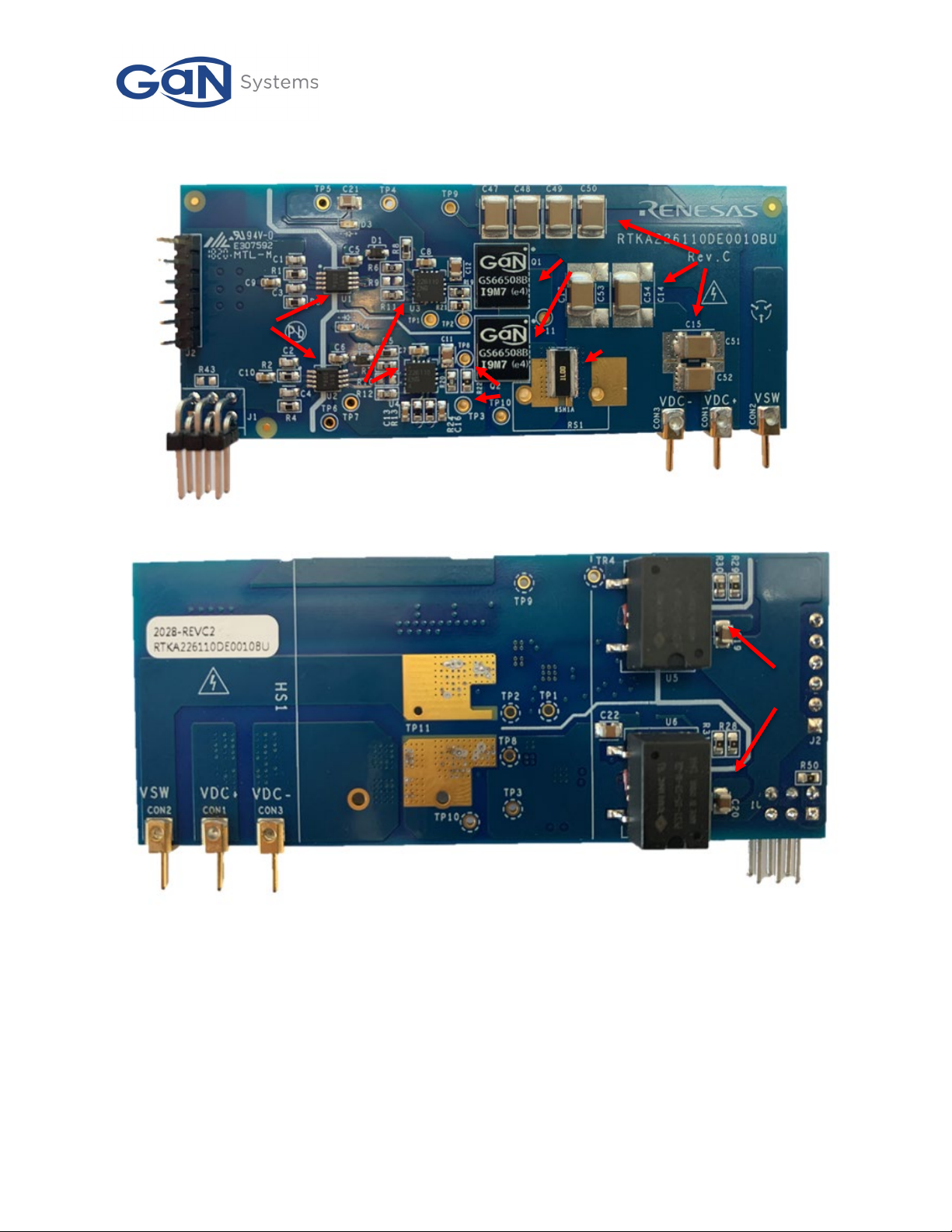
GS-EVB-HB-66508B-RN half bridge daughter board
Figure 2 GS-EVB-HB-66508B-RN top side
Figure 3 GS-EVB-HB-66508B-RN bottom side
A. 2x GaN Systems 650V E-HEMT GS66508B, 30A/50mΩ.
B. Decoupling capacitors C14-C17 and C47-C54.
C. Signal isolator IL611-1E.
D. GaN driver RAA226110.
E. OCP shunt.
F. TP8(gate) and TP3(source) test points for bottom Q2 V
G. 5V-9V isolated DC/DC gate drive power supply
GS.
GS-EVB-HB-66508B-RN Rev. 210118 © 2021 GaN Systems Inc. www.gansystems.com 4
Please refer to the Evaluation Board/Kit Important Notice on page 26
GS-EVB-HB-66508B-RN Technical Manual
_____________________________________________________________________________________________________________________
GaN E-HEMTs:
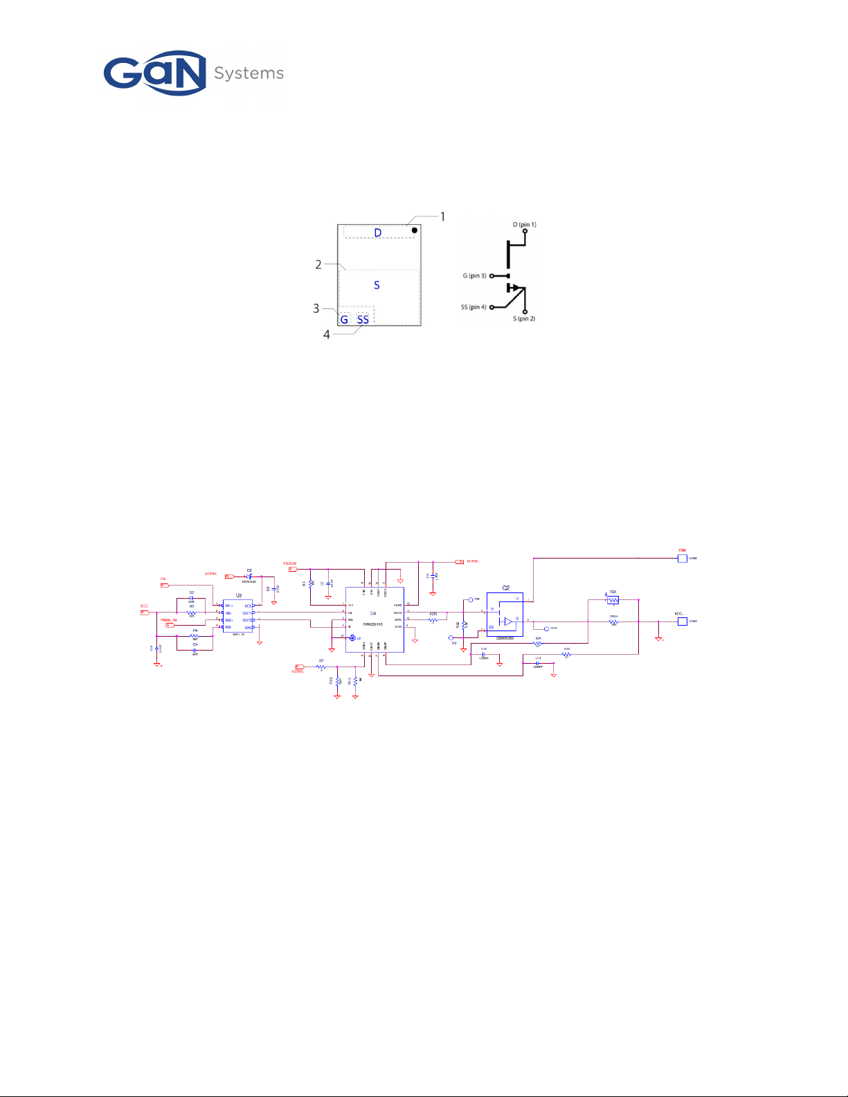
• This daughter board includes two GaN Systems E-HEMT GS66508B (650V/30A, 50mΩ) in a
GaNPx™ B type package. The large S pad serves as source connection and thermal pad. The pin
4 is the kelvin source connection for gate drive return.
Figure 4 Package outline of GS66508B
Gate driver circuit:
• Renesas RAA226110 low-side gate driver is chosen for this design. This driver provides 5.8V gate
drive with 3.8V UVLO. It supports the 5.8V turn on and -3V/0V turn off. It has separated source
and sink drive outputs which eliminates the need for additional diode. OCP is also integrated in
the driver.
• RAA226110 provides configurable source current(0.3A/0.75A/2A) to adjust the slew rate of
GS66508B without gate resistor to minimize the gate loop. The turn off speed can be directly
controlled by the gate resistor Rg_off (R19/R20).
Figure 5 Gate driver circuit
Gate drive power supply:
• 5V-9V isolated DC/DC converters are used for gate drive. The RAA226110 accpets 4.5V to 18V
VDD input voltage. DC/DC conterter 9V output is directly connected to RAA226110.
GS-EVB-HB-66508B-RN Rev. 210118 © 2021 GaN Systems Inc. www.gansystems.com 5
Please refer to the Evaluation Board/Kit Important Notice on page 26
GS-EVB-HB-66508B-RN Technical Manual
Q2 source
Shunt
_____________________________________________________________________________________________________________________
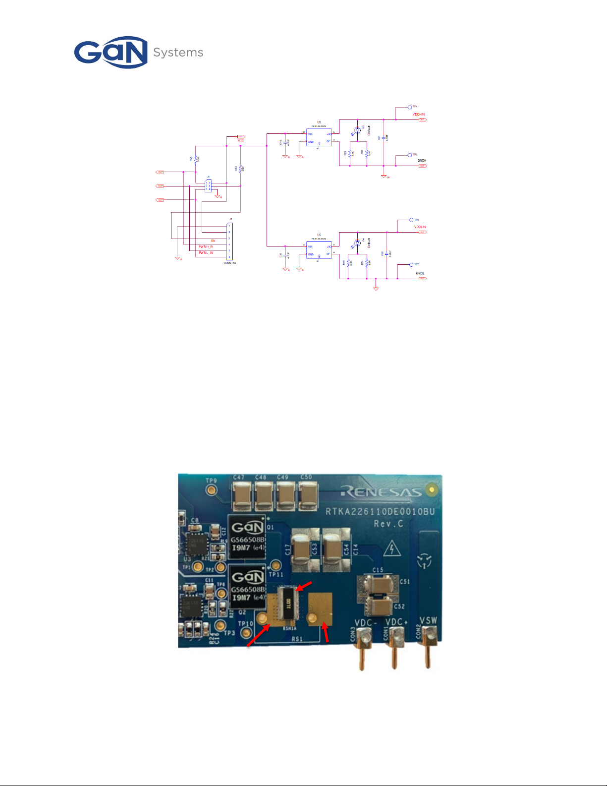
Figure 6 Gate drive power supply
Current shunt:
• The board provides an optional current shunt position E(figure2) between the source of Q2 and
power ground return. This allows drain current measurement for switching characterization test
such as Eon/Eoff measurement.
• The current shunt is also used to provide the OCP signal for the RAA226110 to trigger OCP. The
OCP threchold voltage 40mV/80mV/120mV can be configured through the IDSET pin of
RAA226110.
• If current shunt is not used position E must be shorted.
Figure 7 Current shunt position E
GS-EVB-HB-66508B-RN Rev. 210118 © 2021 GaN Systems Inc. www.gansystems.com 6
Please refer to the Evaluation Board/Kit Important Notice on page 26
GS-EVB-HB-66508B-RN Technical Manual
CAUTION:
before powering up.
VGL
VSL
VSW
BNC case
To oscilloscope
probe input (use
50Ω termination)
BNC tip
V
DS
V
GS
I
D
_____________________________________________________________________________________________________________________
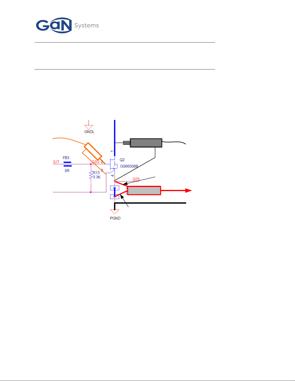
Measurement with current shunt:
1. When measuring VSW with current shunt, ensure all channel probe grounds and current shunt
2. The output of coaxial current shunt can be connected to oscilloscope via 50Ω termination
3. The measured current is inverted and can be scaled by using: Id=Vid/Rshunt.
Check the shunt position E before the first time use. To complete the circuit
position E needs to be either shorted or a current shunt must be inserted
BNC output case are all referenced to the source end of Q2 before the current shunt. The
recommended setup of probes is shown as below.
impedance to reduce the ringing.
Figure 8 Recommended probe connection with current shunt
Thermal design:
1. GS66508B has a thermal pad at the bottom side for heat dissipation. The heat is transferred to the
bottom side of PCB using thermal vias and copper plane.
2. A heatsink (35x35mm size) can be attached to the bottom side of board for optimum cooling.
Thermal Interface Material (TIM) is needed to provide electrical insulation and conformance to
the PCB surface. The daughter board evaluation kit supplies with a sample 35x35mm fin heatsink
(not installed), although other heatsinks can also be used to fit users’ system design.
®
3. A thermal tape type TIM (Berguist
heatsink has the thermal tape pre-applied so simply peel off the protective film and attach the
heatsink to the back of board as marked in Figure 3.
4. Two optional mounting holes as shown in Figure 9 are provided for mounting customized
heatsink using screws.
5. Using the supplied heatsink and TIM, the overall junction to ambient thermal resistance R
~9°C/W with 500LFM airflow.
6. Forced air cooling is recommended for power testing.
GS-EVB-HB-66508B-RN Rev. 210118 © 2021 GaN Systems Inc. www.gansystems.com 7
Please refer to the Evaluation Board/Kit Important Notice on page 26
Bond-Ply 100) is chosen for its easy assembly. The supplied
thJ-A is
GS-EVB-HB-66508B-RN Technical Manual
temperature exceeding T
J_MAX
(150°C)
12
V INPUT
(+)
5V Power Supply
CIN
VSW
PWM control & dead
time circuit
Daughter Board
Probing point for VSW
For Ext.
12VDC Fan
Airflow direction
Optional Cout
VDC-
VOUT
VDC-
VDC+
_____________________________________________________________________________________________________________________
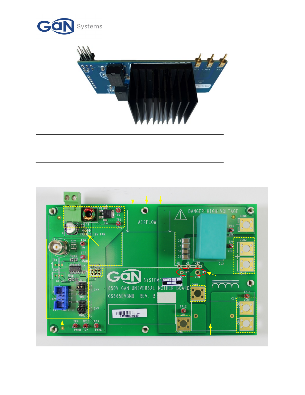
Figure 9 The daughter board with heatsink attached
CAUTION:
Using GS-EVB-HB-66508B-RN with universal mother board GS665MB-EVB
There is no on-board over-temperature protection. Device temperature must
be closely monitored during the test. Never operate the board with device
GS-EVB-HB-66508B-RN Rev. 210118 © 2021 GaN Systems Inc. www.gansystems.com 8
Figure 10 650V universal mother board GS665MB-EVB
Please refer to the Evaluation Board/Kit Important Notice on page 26
GS-EVB-HB-66508B-RN Technical Manual
0V
D1 PMEG2005EB
SOD523
R6
1K00
TR12K
C11
100pF
0V
R5
1K00
C10
1uF
C9
0.1uF
+5V
J7
112538
1
2
3
4
5
R4
100R
R1206
R2
100R
R1206
U2A
74VHC132
3
1
2
14
7
0V
R1
49R9
0V
D2 PMEG2005EB
SOD523
TR22K
C12
100pF
0V
U2B
74VHC132
4
5
6
U2C
74VHC132
9
10
8
U2D
74VHC132
12
13
11
TP7
TP8
DNP
DNP
PWM
OUTPUT
INVERTED
PW M OUTPUT
R3
49R9
DNP
DNP
R7
49R9
_____________________________________________________________________________________________________________________
GaN Systems provides a universal 650V mother board (ordering part number: GS665MB-EVB, sold
separately) that can be used as the basic evaluation platform for all the daughter boards.
The universal 650V mother board evaluation kit includes following items:
1. Mother board GS665MB-EVB
2. 12VDC Fan
12V input:
The board can be powered by 9-12V on J1. On-board voltage regulator creates to 5V for daughter board
and control logic circuits. J3 is used for external 12VDC fan.
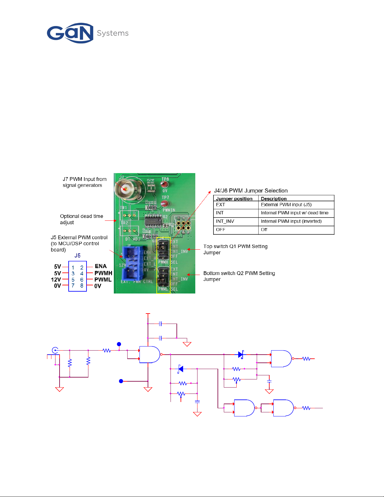
PWM control circuit:
Figure 11 PWM control input and dead time circuit
Please refer to the Evaluation Board/Kit Important Notice on page 26
Figure 12 On board dead time generatrion circuit
The top and bottom switches PWM inputs can be individually controlled by two jumpers J4 and J6. Users
can choose between a pair of complementary on-board internal PWM signals (non-inverted and inverted,
GS-EVB-HB-66508B-RN Rev. 210118 © 2021 GaN Systems Inc. www.gansystems.com 9
 Loading...