

Page 1
Description
GM6250 combine high accuracy with very low power con-
sumption, and provides high output current even when the
application requires extremely low input-output voltage dif-
ferential.
GM6250 includes a precision voltage reference, an error
correction circuit, over-temperature protection, and a cur-
rent limited output driver. Fast transient response to load
variations provides excellent stability under dynamic load
conditions.
GM6250 comes in SOT-23 (150mW), SOT-89 (500mW)
and TO-92 packages.
Features
Maximum output current 250mA (within
maximum power dissipation)
Output voltage: from 1.8 V to 5.0V in 0.1V
increments
Output voltage ±2%
CMOS low power consumption, typically
1.0µA at V = 5.0V
Input stability typically 0.2%/ V
Ultra-low dropout voltage 0.38V @ I =
200mA at V = 5.0V
Small input/ output differential:
0.4V at 160mA (V = 3.3V)
SOT-23 (150mW), SOT-89 (500mW) and
TO-92 packages
OUT
OUT
OUT
OUT
Application
Palmtops
Portable Cameras
Video Recorders
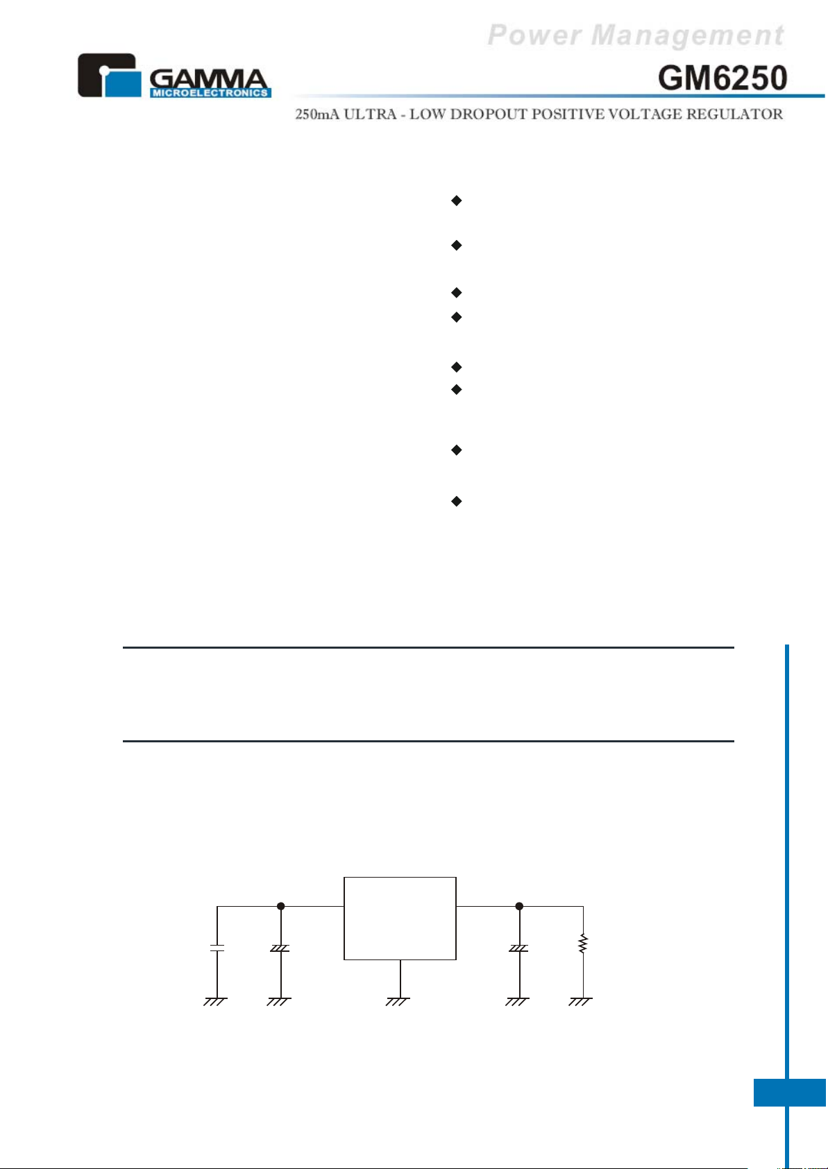
TYPICAL APPLICATION CIRCUITS
GM6250
V
IN
V
IN
+ +
C
IN
1µF
(Tantalum)
Battery Powered Equipment
Reference Voltage Sources
V
OUT
V
SS
C
L
1µF
(Tantalum)
R
L
www.gammamicro.com
GM6250 V0.1
1
Page 2
MARKING INFORMATION & PIN CONFIGURATIONS (TOP VIEW)
SOT-89
GM6250
VVAYWW
1
V
SS
3
2
V
V
OUT
IN
(EA = GM6250)
SOT-23
XXVYW
1
V
SS
TO-92
6250
V
IN
3
2
V
OUT
VV
AYWW
1 2 3
1. V
2. V
3. V
SS
IN
OUT
XX = Marking Code
V = Voltage Code
VV = Voltage Suffix (18=1.8V, 50=5.0V)
A = Assembly Location
Y = Year
WW, W= Weekly
Shipping
1,000 Units/ ESD Bag
2,000 Units/ Ammo Pack (Tape)
3,000 Units/ Tape and Reel
1,000 Units/ Tape and Reel
1,000 Units/ ESD Bag
2,000 Units/ Ammo Pack (Tape)
3,000 Units/ Tape and Reel
1,000 Units/ Tape and Reel
1,000 Units/ ESD Bag
2,000 Units/ Ammo Pack (Tape)
3,000 Units/ Tape and Reel
1,000 Units/ Tape and Reel
1,000 Units/ ESD Bag
2,000 Units/ Ammo Pack (Tape)
3,000 Units/ Tape and Reel
1,000 Units/ Tape and Reel
1,000 Units/ ESD Bag
2,000 Units/ Ammo Pack (Tape)
3,000 Units/ Tape and Reel
1,000 Units/ Tape and Reel
1,000 Units/ ESD Bag
2,000 Units/ Ammo Pack (Tape)
3,000 Units/ Tape and Reel
1,000 Units/ Tape and Reel
1,000 Units/ ESD Bag
2,000 Units/ Ammo Pack (Tape)
3,000 Units/ Tape and Reel
1,000 Units/ Tape and Reel
GM6250
ORDERING INFORMATION (Continued)
Ordering Number
GM6250-1.5T92B
GM6250-1.5T92RL
GM6250-1.5ST23R
GM6250-1.5ST89R
GM6250-1.8T92B
GM6250-1.8T92RL
GM6250-1.8ST23R
GM6250-1.8ST89R
GM6250-2.5T92B
GM6250-2.5T92RL
GM6250-2.5ST23R
GM6250-2.5ST89R
GM6250-2.7T92B
GM6250-2.7T92RL
GM6250-2.7ST23R
GM6250-2.7ST89R
GM6250-2.8T92B
GM6250-2.8T92RL
GM6250-2.8ST23R
GM6250-2.8ST89R
GM6250-2.85T92B
GM6250-2.85T92RL
GM6250-2.85ST23R
GM6250-2.85ST89R
GM6250-3.0T92B
GM6250-3.0T92RL
GM6250-3.0ST23R
GM6250-3.0ST89R
Output Voltage
1.5V
1.5V
1.5V
1.5V
1.8V
1.8V
1.8V
1.8V
2.5V
2.5V
2.5V
2.5V
2.7V
2.7V
2.7V
2.7V
2.8V
2.8V
2.8V
2.8V
2.85V
2.85V
2.85V
2.85V
3.0V
3.0V
3.0V
3.0V
Voltage Code
Package
TO-92
TO-92
C
E
G
T
H
I
J
SOT-23
SOT-89
TO-92
TO-92
SOT-23
SOT-89
TO-92
TO-92
SOT-23
SOT-89
TO-92
TO-92
SOT-23
SOT-89
TO-92
TO-92
SOT-23
SOT-89
TO-92
TO-92
SOT-23
SOT-89
TO-92
TO-92
SOT-23
SOT-89
2
* For detail Ordering Number identification, please see last page.
Page 3
ORDERING INFORMATION (Continued)
Ordering Number
GM6250-3.2T92B
GM6250-3.2T92RL
GM6250-3.2ST23R
GM6250-3.2ST89R
GM6250-3.3T92B
GM6250-3.3T92RL
GM6250-3.3ST23R
GM6250-3.3ST89R
GM6250-3.5T92B
GM6250-3.5T92RL
GM6250-3.5ST23R
GM6250-3.5ST89R
GM6250-3.6T92B
GM6250-3.6T92RL
GM6250-3.6ST23R
GM6250-3.6ST89R
GM6250-4.0T92B
GM6250-4.0T92RL
GM6250-4.0ST23R
GM6250-4.0ST89R
GM6250-4.4T92B
GM6250-4.4T92RL
GM6250-4.4ST23R
GM6250-4.4ST89R
GM6250-4.5T92B
GM6250-4.5T92RL
GM6250-4.5ST23R
GM6250-4.5ST89R
GM6250-5.0T92B
GM6250-5.0T92RL
GM6250-5.0ST23R
GM6250-5.0ST89R
Output Voltage
3.2V
3.2V
3.2V
3.2V
3.3V
3.3V
3.3V
3.3V
3.5V
3.5V
3.5V
3.5V
3.6V
3.6V
3.6V
3.6V
4.0V
4.0V
4.0V
4.0V
4.4V
4.4V
4.4V
4.4V
4.5V
4.5V
4.5V
4.5V
5.0V
5.0V
5.0V
5.0V
Voltage Code
U
K
V
L
M
W
N
Q
Package
TO-92
TO-92
SOT-23
SOT-89
TO-92
TO-92
SOT-23
SOT-89
TO-92
TO-92
SOT-23
SOT-89
TO-92
TO-92
SOT-23
SOT-89
TO-92
TO-92
SOT-23
SOT-89
TO-92
TO-92
SOT-23
SOT-89
TO-92
TO-92
SOT-23
SOT-89
TO-92
TO-92
SOT-23
SOT-89
Shipping
1,000 Units/ ESD Bag
2,000 Units/ Ammo Pack (Tape)
3,000 Units/ Tape and Reel
1,000 Units/ Tape and Reel
1,000 Units/ ESD Bag
2,000 Units/ Ammo Pack (Tape)
3,000 Units/ Tape and Reel
1,000 Units/ Tape and Reel
1,000 Units/ ESD Bag
2,000 Units/ Ammo Pack (Tape)
3,000 Units/ Tape and Reel
1,000 Units/ Tape and Reel
1,000 Units/ ESD Bag
2,000 Units/ Ammo Pack (Tape)
3,000 Units/ Tape and Reel
1,000 Units/ Tape and Reel
1,000 Units/ ESD Bag
2,000 Units/ Ammo Pack (Tape)
3,000 Units/ Tape and Reel
1,000 Units/ Tape and Reel
1,000 Units/ ESD Bag
2,000 Units/ Ammo Pack (Tape)
3,000 Units/ Tape and Reel
1,000 Units/ Tape and Reel
1,000 Units/ ESD Bag
2,000 Units/ Ammo Pack (Tape)
3,000 Units/ Tape and Reel
1,000 Units/ Tape and Reel
1,000 Units/ ESD Bag
2,000 Units/ Ammo Pack (Tape)
3,000 Units/ Tape and Reel
1,000 Units/ Tape and Reel
* For detail Ordering Number identification, please see last page.
GM6250
Page 4
ABSOLUTE MAXIMUM RATINGS
PARAMETER
Input Voltage
Output Current
Output Voltage
Continuous Total Power
Dissipation
Operating Ambient Temperature
Storage Temperature
Thermal Information
PARAMETER
Thermal Resistance R
Thermal Resistance R
jc
ja
SOT - 23
SOT - 89
TO - 92
SOT-89
SYMBOL RATINGS
12
500
SS IN
150
500
300
-30 ~ +80
-40 ~ +125
I
V
T
V
OUT
OUT
P
opr
T
stg
IN
V - 0.3 ~ V + 0.3
D
Maximum Unit
100
300
UNITS
V
mA
V
mW
°C
°C
°C/ W
°C/ W
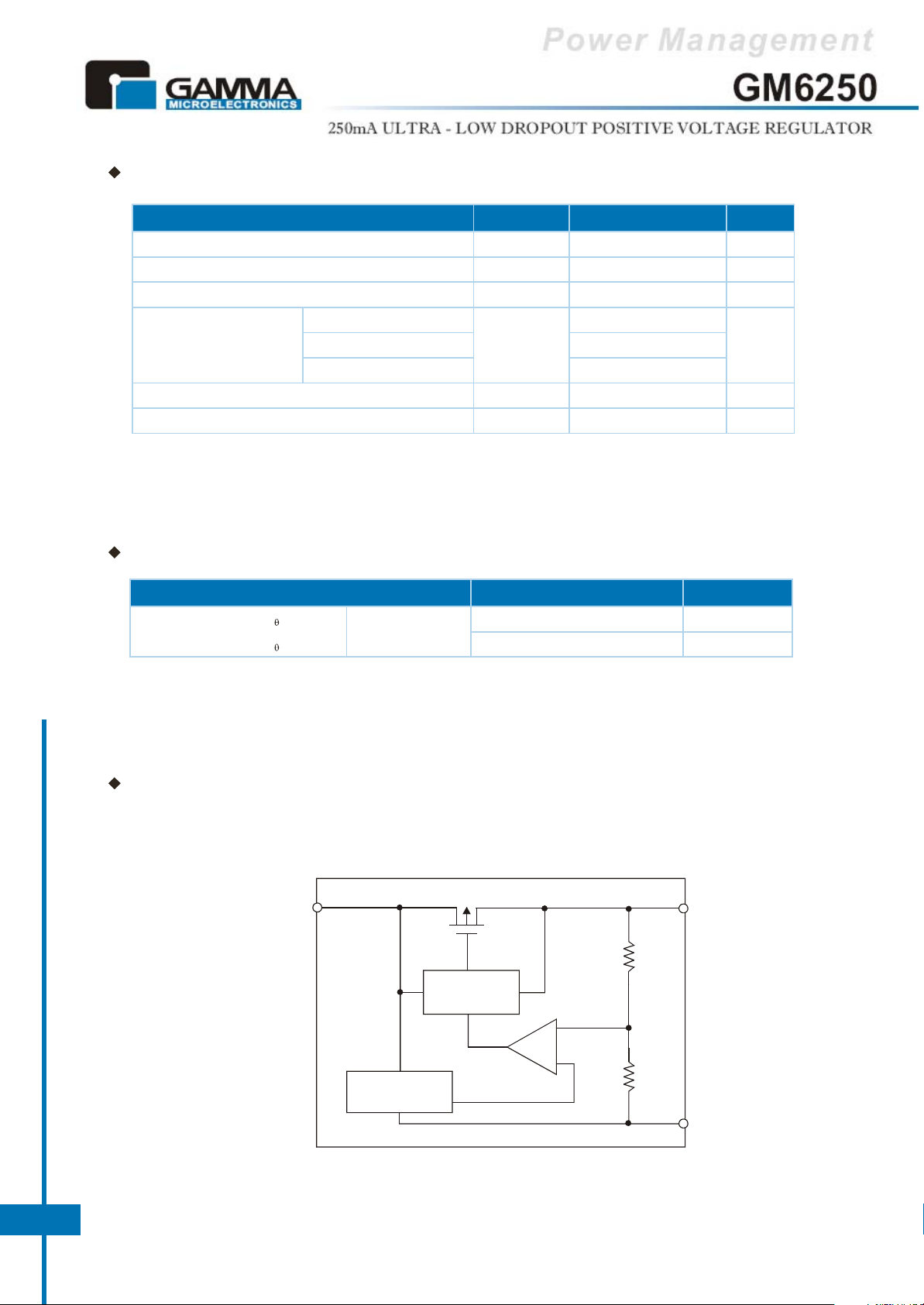
BLOCK DIAGRAM
V
IN
Current Limiter
+
-
Voltage
Reference
V
V
OUT
SS
GM6250
4
Page 5

ELECTRICAL CHARACTERISTICS (T = 25°C unless otherwise noted)
A
Parameter
Output Voltage
Maximum Output Current
GM6250-1.5V
GM6250-1.8V
GM6250-2.5V
GM6250-2.7V
GM6250-2.8V
GM6250-3.0V
GM6250-3.2V
GM6250-3.3V
GM6250-3.5V
GM6250-3.6V
GM6250-4.0V
GM6250-4.4V
GM6250-4.5V
GM6250-5.0V
GM6250-1.5V
GM6250-1.8V
GM6250-2.5V
GM6250-2.7V
GM6250-2.8V
GM6250-3.0V
GM6250-3.2V
GM6250-3.3V
GM6250-3.5V
GM6250-3.6V
GM6250-4.0V
GM6250-4.4V
GM6250-4.5V
GM6250-5.0V
Symbol
V (E)
OUT
I max
OUT
Condition
(Note 2)
I =40mA,
OUT
V >VDrop+V
IN
V =3.0V, V (E) 1.35V
IN OUT
V =3.0V, V (E) 1.62V
IN OUT
V =4.0V, V (E) 2.3V
IN OUT
V =4.0V, V (E) 2.43V
IN OUT
V =4.0V, V (E) 2.52V
IN OUT
V =4.0V, V (E) 2.7V
IN OUT
V =4.0V, V (E) 2.88V
IN OUT
V =4.0V, V (E) 2.97V
IN OUT
V =5.0V, V (E) 3.15V
IN OUT
V =5.0V, V (E) 3.24V
IN OUT
V =5.0V, V (E) 3.6V
IN OUT
V =6.0V, V (E) 3.96V
IN OUT
V =6.0V, V (E) 4.05V
IN OUT
V =6.0V, V (E) 4.5V
IN OUT
OUT
Min
1.470
1.764
2.450
2.646
2.744
2.940
3.136
3.234
3.430
3.528
3.920
4.312
4.410
4.900
250
Typ
1.500
1.800
2.500
2.700
2.800
3.000
3.200
3.300
3.500
3.600
4.000
4.400
4.500
5.000
Max
1.530
1.836
2.550
2.754
2.856
3.060
3.264
3.366
3.570
3.672
4.080
4.488
4.590
5.100
Unit Circuit
V
mA
1
1
GM6250
5
Page 6

ELECTRICAL CHARACTERISTICS (T = 25°C unless otherwise noted)
A
Parameter
Load Stability
Input - Output
Voltage Differential
(Note 3)
GM6250-1.5V
GM6250-1.8V
GM6250-2.5V
GM6250-2.7V
GM6250-2.8V
GM6250-3.0V
GM6250-3.2V
GM6250-3.3V
GM6250-3.5V
GM6250-3.6V
GM6250-4.0V
GM6250-4.4V
GM6250-4.5V
GM6250-5.0V
GM6250-1.5V
GM6250-1.8V
GM6250-2.5V
GM6250-2.7V
GM6250-2.8V
GM6250-3.0V
GM6250-3.2V
GM6250-3.3V
GM6250-3.5V
GM6250-3.6V
GM6250-4.0V
GM6250-4.4V
GM6250-4.5V
GM6250-5.0V
Symbol
DV
OUT
Vdif1
Vdif2
Vdif1
Vdif2
Vdif1
Vdif2
Vdif1
Vdif2
Vdif1
Vdif2
Vdif1
Vdif2
Vdif1
Vdif2
Vdif1
Vdif2
Vdif1
Vdif2
Vdif1
Vdif2
Vdif1
Vdif2
Vdif1
Vdif2
Vdif1
Vdif2
Vdif1
Vdif2
Condition
V =2.5V, 1mA I 60mA
IN OUT
V =2.8V, 1mA I 60mA
IN OUT
V =3.5V, 1mA I 80mA
IN OUT
V =3.7V, 1mA I 80mA
IN OUT
V =3.8V, 1mA I 80mA
IN OUT
V =4.0V, 1mA I 80mA
IN OUT
V =4.2V, 1mA I 80mA
IN OUT
V =4.3V, 1mA I 100mA
IN OUT
V =4.5V, 1mA I 100mA
IN OUT
V =4.6V, 1mA I 100mA
IN OUT
V =5.0V, 1mA I 100mA
IN OUT
V =5.4V, 1mA I 100mA
IN OUT
V =4.5V, 1mA I 100mA
IN OUT
V =6.0V, 1mA I 100mA
IN OUT
I = 40mA
OUT
I = 160mA
OUT
I = 60mA
OUT
I = 160mA
OUT
I = 80mA
OUT
I = 160mA
OUT
I = 80mA
OUT
I = 160mA
OUT
I = 80mA
OUT
I = 160mA
OUT
I = 80mA
OUT
I = 160mA
OUT
I = 80mA
OUT
I = 160mA
OUT
I = 100mA
OUT
I = 200mA
OUT
I = 100mA
OUT
I = 200mA
OUT
I = 100mA
OUT
I = 200mA
OUT
I = 100mA
OUT
I = 200mA
OUT
I = 100mA
OUT
I = 200mA
OUT
I = 100mA
OUT
I = 200mA
OUT
I = 100mA
OUT
I = 200mA
OUT
Min
Typ
45
45
45
45
45
45
45
45
45
45
40
40
40
40
180
900
180
900
180
550
180
400
180
400
180
400
180
400
170
400
120
380
120
380
170
400
120
380
120
380
120
380
Max
90
90
90
90
90
90
90
90
90
90
80
80
80
80
360
1300
360
1300
360
850
360
700
360
700
360
700
360
700
330
630
300
600
300
600
330
630
300
600
300
600
300
600
Unit Circuit
mV
mV
1
1
GM6250
6
Page 7

ELECTRICAL CHARACTERISTICS (T = 25°C unless otherwise noted)
A
Parameter
Supply Current
GM6250-1.5V
GM6250-1.8V
GM6250-2.5V
GM6250-2.7V
GM6250-2.8V
GM6250-3.0V
GM6250-3.2V
GM6250-3.3V
GM6250-3.5V
GM6250-3.6V
GM6250-4.0V
GM6250-4.4V
GM6250-4.5V
GM6250-5.0V
Symbol
I
SS
Condition
V = 1.5V
IN
V = 2.8V
IN
V = 3.5V
IN
V = 3.7V
IN
V = 3.8V
IN
V = 4.0V
IN
V = 4.2V
IN
V = 4.3V
IN
V = 4.5V
IN
V = 4.6V
IN
V = 5.0V
IN
V = 5.4V
IN
V = 5.5V
IN
V = 6.0V
IN
Output Current Limit
I = 40mA
GM6250-1.5V
GM6250-1.8V
GM6250-2.5V
GM6250-2.7V
GM6250-2.8V
GM6250-3.0V
GM6250-3.2V
DV
Input Stability
GM6250-3.3V
OUT
DVIN • VOUT
GM6250-3.5V
GM6250-3.6V
GM6250-4.0V
GM6250-4.4V
GM6250-4.5V
GM6250-5.0V
Input Voltage
Output Voltage
Temperature Characteristics
Note: 1. V (T) = Specified Output Voltage
2. V (E) = Effective Output Voltage (the output voltage when"V (T) + 1.0V" is provided at the V pin while
maintaining a certain I value)
3. Vdif = { V 1 (Note 4) - V (E)}
4. V 1 = The input voltage at the time 98% of V (E) is output (input voltage has been gradually reduced).
* Output Voltage from 1.8V to 6.0V in 0.1V increments ate available
OUT
OUT OUT IN
IN OUT
IN OUT
V
IN
DV
OUT
DTopr • VOUT
OUT
OUT
2.5V V 10.0V
IN
I = 40mA
OUT
2.8V V 10.0V
IN
I = 40mA
OUT
3.5V V 10.0V
IN
I = 40mA
OUT
3.7V V 10.0V
IN
I = 40mA
OUT
3.8V V 10.0V
IN
I = 40mA
OUT
4.0V V 10.0V
IN
I = 40mA
OUT
4.2V V 10.0V
IN
I = 40mA
OUT
4.3V V 10.0V
IN
I = 40mA
OUT
4.5V V 10.0V
IN
I = 40mA
OUT
4.6V V 10.0V
IN
I = 40mA
OUT
5.0V V 10.0V
IN
I = 40mA
OUT
5.4V V 10.0V
IN
I = 40mA
OUT
5.5V V 10.0V
IN
I = 40mA
OUT
6.0V V 10.0V
IN
I = 10mA
OUT
-30°C Topr 80°C
Min
Typ
1.0
500
0.2
±100
Max
2.9
0.3
10
Unit Circuit
µA
mA
%/ V
V
ppm/°C
2
-
1
-
1
GM6250
7
Page 8

DIRECTIONS FOR USAGE
Notes on Usage
1. Please use this IC within the stipulated absolute maximum ratings as the IC is liable to malfunction
outside of such parameters.
2. There is a possibility theat, oscillation may occur as a result of the impedance present between the
power supply and the IC's input. Where impedance is 10W or more, please use a capacitor (C )
IN
of at least 1µF.
With a large output current, operations can be stabilised by increasing capacitor size (C ). If C is
small and capacitor size (C ) is increased, there is a possibility of oscillation due to input impedance.
In such cases, operations can be stabilised by either increasing the size of C or decreasing the size of C .
3. Please ensure the output current (I ) is less than Pd ÷ (V - V ) and does not exceed the
L
IN L
OUT IN OUT
IN IN
stipulated continuous total power dissipation value (Pd) for the package.
TEST CIRCUIT
Circuit 1
GM6250
V
IN
V
O
A
V
IN
Circuit 2
+ +
1µF
(Tantalum)
V
SS
(Tantalum)
GM6250
V
IN
V
IN
V
V
SS
A
1µF
O
V
Open
R
L
CALCULATING POWER DISSIPATION
The GM6250 series precision linear regulators include thermal shutdown and current limit circuitry to
protect the devices. However, high power regulators normally operate at high junction temperatures so it
is important to calculate the power dissipation and junction temperatures accurately to be sure that you
use and adequate heat sink.
The thermal characteristics of an IC depend four factors:
1. Maximum Ambient Temperature T (°C)
2. Power Dissipation P (Watts)
D
3. Maximum Junction Temperature T (°C)
4. Thermal Resistance Junction to ambient R (°C/W)
These relationship of these four factors is expressed by equation (1): T = T + P X R
GM6250
8
Maximum ambient temperature and power dissipation are determined by the design while the maximum
junction temperature and thermal resistance depend on the manufacturer and the package type.
A
J
JA
Q
JAD QJA
Page 9

PERFORMANCE CHARACTERISTICS FOR GM6250 - 3.0
3.1
3.0
T
OUT
2.9
Output Voltage: V (V)
2.8
2.7
0 20 40 60 80 100 120 140 160 180
= 25°C
opr
Output Current: I (mA)
OUT
Figure 1: Output Voltage vs.
3.20
3.00
OUT
2.80
2.60
Output Voltage: V (V)
2.40
2.20
2.5 3.0 3.5
Output Current
I =1mA
OUT
10mA
Input Voltage: V (V)
40mA
IN
Figure 3: Output Voltage vs.
Input voltage
V =4V
IN
C =1µF
IN
C =1µF
L
T = 25°C
opr
C =1µF
IN
C =1µF
L
1.0
C =1µF
IN
C =1µF
L
0.8
DIF
0.6
0.4
0.2
Input/ Output Voltage Diff.: V (V)
0.0
-0.2
0 20 40 60 80 100 120 140 160 180
T
= 25°C
opr
Output Current: I (mA)
OUT
Figure 2: Input/ Output Voltage differential
vs. Output Current
3.10
3.05
3.00
OUT
I =1mA
OUT
40mA
2.95
Output Voltage: V (V)
2.90
2.85
3 4 5 6 7 8 9 10
Input Voltage: V (V)
Figure 4: Output Voltage vs.
Input voltage
IN
T = 25°C
opr
C =1µF
IN
C =1µF
L
10mA
3.0
T
= 25°C
opr
2.0
SS
1.0
Supply Current: I (µA)
0
0 2 4 6 8 10
Input Voltage: V (V)
IN
Figure 5: Supply Current vs. Input
Voltage
2.50
2.25
SS
2.00
Supply Current: I (µA)
1.75
1.50
3 4 5 6 7 8 9 10
Input Voltage: V (V)
T
opr
IN
= 25°C
Figure 6: Supply Current vs.
Input Voltage
GM6250
9
Page 10

PERFORMANCE CHARACTERISTICS FOR GM6250 - 3.0
6
4
2
IN
0
-2
Input Voltage: V (V)
-4
-6
Time (0.4msec/ div)
Input Voltage
Output Voltage
I = 1mA
OUT
C =1µF
L
Figure 7: Input Transient Response 1
60
50
40
30
20
10
Ripple Rejection Rate :RR (dB)
0
0.01 0.1 1 10
V = 4V +1V AC
IN DC P-P
I = 40mA, C = 1µF
OUT L
Ripple Frequency: f (kHz)
6
5
4
OUT
3
2
Output Voltage: V (V)
1
0
6
5
IN
4
3
Input Voltage: V (V)
2
1
Input Voltage
I = 1mA
OUT
C =1µF
L
Output Voltage
Time (1msec/ div)
5.0
4.5
4.0
3.5
3.0
2.5
OUT
Output Voltage: V (V)
Figure 8: Input Transient Response 2
Figure 9: Ripple Rejection Rate
TO-92 PACKAGE OUTLINE DIMENSIONS
4.6 ± 0.1
4.6 ± 0.1
2.3
1.45 ± 0.1
14.5 ± 0.5
1.27 1.27
3 - 0.46
3.6 ± 0.15
2° 2°
2° 2°
0.38 ± 0.015
10
GM6250
3.6 ± 0.15
Unit: mm
1.3 ± 0.1
5° 5°
Page 11

SOT-89 PACKAGE OUTLINE DIMENSIONS
4.20 ± 0.05
R 0.13~4X
2.5 ± 0.05
1.00 ± 0.07
6°~2X
6°~2X
4.50 ± 0.05
1.650 REF
1.400 REF
1.50 1.50
3.00 ± 0.025
R 0.13~3X
0.46 ± 0.025
R 0.13~2X
R 0.13~2X
6°
1.50 ± 0.05
0.38 ± 0.01
Unit: mm
NO DRAFT~2
R 0.1 MAX
Pad Layout
45°
1.5
Units: mm
2
3
0.7
1.5
1
SOT-23 PACKAGE OUTLINE DIMENSIONS
2.90 ± 0.1
0.4 ± 0.1
2.8 ± 0.1
0.95 ± 0.038
1.9 ± 0.05
5°
1.5 ± 0.05
0.65 ± 0.05
0.8 ± 0.05
1.10 ± 0.1
0.13
Unit: mm
0~0.1
Pad Layout
0.035
0.9
0.037
0.95
0.031
0.8
0.037
0.95
0.079
2.0
Inches
( )
mm
11
GM6250
Page 12

ORDERING NUMBER
GM 6250 1.8 T92 B
Gamma Micro.
Circuit Type
Output Voltage
1.8: 1.8, 2.5: 2.5V
2.7: 2.7V, 2.8: 2.8V
3.0: 3.0V, 3.3: 3.3V,
3.6: 3.6V, 4.0: 4.0V
Shipping
B: ESD Bag
RL: Ammo Pack (Tape)
T: Tube
R: Tape & Reel
Package
T92: TO-92
ST3: SOT-23
ST89: SOT89
12
GM6250
Page 13

13
GM6250
 Loading...