

Page 1

Service Manual
ML Series
Page 2

Table of Contents
Operating Instructions 3
Troubleshooting Instructions 8
Output Disabling 10
Preamp Description 12
Power Supply Start-up 15
ML/E Turn-On Procedure 19
ML/S Turn-On Procedure 21
Schematics 27
Engineering Change Orders (ECOs) 38
ML/S Bill of Materials 53
ML/E Bill of Materials 60
Page 3
Page 4
Page 5
Page 6
Page 7
Page 8

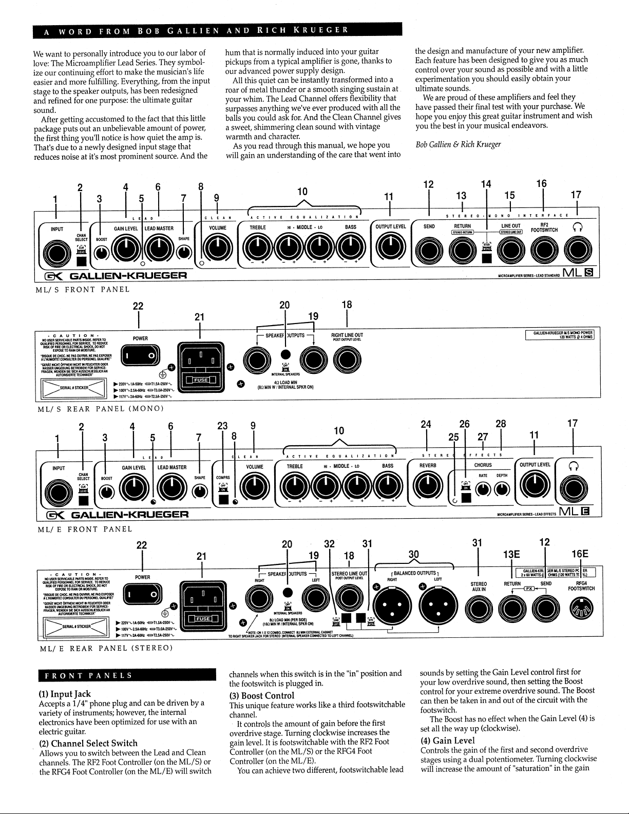
Microamplifier Series- Lead
Disassembly and Preliminary Troubleshooting Procedure
GK Document # 426-0063-A
Model #’s: ML260E, ML260S, ML120E, ML120S- all options
2/15/91 Rev. 9/10/99 SW
Disassembly Procedure
1) Remove the bottom cover first by removing the six # 6 screws on the bottom and the three # 6 screws on each side. One side has an extra
screw which may require a # 4 screwdriver. Note that the center screw on each side is a machine screw and will need to be returned to the
tapped hole in the side of the heat sink when reassembling the unit. On a combo unit, removing only the side screws will allow the
electronics to be lifted away from the speaker compartment. The wires connecting the speaker to the electronics should then be detached
from the power amp.
2a) ML-S: The ML-S preamp removes easily by removing the three # 6 flat head screws attaching the front panel to the heat sink.
2b) ML-E: The ML-E preamp requires the same three screws to be removed. Also, at the rear panel, remove the two # 2 screws that
secure the RFG4 jack and the two # 6 screws holding the balanced outs in place. Using a 15mm nut driver, remove the plastic nuts from the
Stereo Aux. In, Return, and Send jacks. Pull the preamp board out and away from the rear panel being careful not to lose the fiber washers
from the ¼” jacks.
3) The two separate parts- the power amp/power supply attached to the heat sink, and the preamp board- can be set on a flat surface with the
component sides facing up and the wires remaining connected. The required troubleshooting can be done.
Problems with the Amp- Where to Look for Help
This short troubleshooting guide will attempt to analyze problems to quickly determine whether preamp, power amp, or power supply related.
Use the power supply/amp troubleshooting guide or the preamp circuit descriptions wherever applicable to fix the problem.
1) Front panel LED’s do not light (no power): Possible blown fuse or other power supply problem; see power supply troubleshooting
procedure.
2) LED’s work but no output from power amp: Could be preamp or power amp problem. First, turn power switch off for 3 seconds, then
back on without input signal to clear shutdown feature. Set all knobs to 10 and put in a signal at 5mVrms. If there is still no output, look
at either end of the red and white wires going between the preamp and power amp with a scope probe. If there is a signal there but no
output, then there is most likely a problem with the power amp. If there is no signal, the problem is in the preamp. Check the wires to
make sure there is a good connection at either end.
3) Distortion at the Output: Follow procedure from #2 above (may want to start with output level on 0 and gradually increase it). This
time, note whether the signal is a clean sine wave like the input, or if it is clipping off part of the signal or has any distortion. If the signal
is clean, the problem is most likely from the power amp. If the signal is cut in half, check the 15V supplies (any LF353- pins 8 & 4 should
have +/- 15VDC). If those supply voltages are not there, or are not clean DC levels, refer to the power supply/amp troubleshooting
procedure. If there isn’t a problem with the 15V supplies but the signal is still distorted, the problem is most likely preamp related.
4) Excessive noise or humming: If the problem goes away when the output level is set to 0, it is probably a preamp problem- often a loose
part or bad jack. If it doesn’t, the power amp/supply has the problem.
5) Amp works OK except for some individual features: Problem is usually in the preamp, but check the footswitch as well.
Scope
This document lists some steps to follow to quickly troubleshoot the microamplifier series of power supplies and power amps. Only common
failures for Rev. E power amps / supplies will be addressed. Previous power supplies used TIP50 transistors, which have different failure
modes. For more detail, this procedure should be used along with the assembly line power supply / amp start-up procedure, GK Document
#420-0071.
NOTE: The following instructions are given with the heat sink on the bench and the rear panel away from the technician.
Page 9

Fuse Inspection
Lightly blown- Very often an amp in service has a blown fuse, and is one of the first things a service tech checks. Sometimes, much can be
determined from the condition of a blown fuse. With the amp series, it is possible that the amp is OK and the fuse is the only problem. a
lightly blown fuse may indicate merely an overload condition that did not trip the overload protection circuit, or a weak
Troubleshooting Procedure (contd.)
fuse. In this case, the element is open in the center, and the ends are intact and visible. If it is suspected that the overload circuit was affected,
refer to the test in the start-up procedure. Also, make sure the unit is equipped with a spare fuse.
A failure in either the +15V or –15V supply may also cause a lightly blown fuse. If the amp had been operating normally for some
time, a preamp problem may exist. To check, remove the wires connecting to the preamp and check the power supply waveform. If OK, the
problem may be in the preamp and a prime suspect may be a TL604, if it has one. If a problem still exists, check the 15V supplies on the
power amp board.
Mildly blown- If the fuse is mildly blown, the power amp may be blown. This type of failure will often result in a fuse with a black band in
the center. Refer to Sec. 3.
Violently blown- If the fuse is violently blown, most of the fuse will look black, the glass body may be cracked an break upon removal. This
usually indicates a blown power supply. See Sec. 5.
Power Amp
Caution! - The power amp must always be operated with the outside output transistors, Q824 and Q759, firmly clamped to the heat sink with
screws through the brass heat clips with A06s inside. These latter transistors, Q823 and Q758, provide feedback for the biasing of the outputs.
Failure to clamp these parts may result in thermal runaway, as the bias current becomes several amps and the transistors operate outside their
safe operating area. Mono amps do not have Q759, but the board needs to be positioned at each end anyway. Always screw down all power
transistors to the heat sink when providing output power for any length of time.Also, the ground must be connected, which is completed by
screwing a 4-40 having a captive lock washer into the hole directly between Q824 and Q808. Make sure the lock washer is not touching the
board. Do not use a flat washer. The heat sink for the hole is not anodized.
Ohm Check of Outputs – Failed output transistors usually measure zero or low for collector to emitter. This turns out to be the two leftmost
terminals. Check all TIP33s and TIP34s. bad transistors will usually have a cracked or broken plastic body. Replace both outputs if one
measures bad. Usually, transistor replacement is all that is necessary to fix the amp, unless some other problem caused the amp to fail. These
other problems are not within the scope to this document. Note that the outputs can be disengaged by moving the clips near the transistor
terminals. The rule is, the transistor is engaged when the clip is closest to the .33 ohm emitter resistor of the transistor.
Auto Shutoff Feature – The unit may be in service to correct the problem of nuisance tripping of the output, usually caused by other
equipment on the same power circuit or by radiating equipment in close proximity. See GK Document #450-0062-01 for an explanation of the
shutdown feature and how to disable it.
Power Supply
Caution! – The two power MOSFETs, (BUK456-800A), must be firmly clamped to the heat sink when powering the amplifier. It is OK to run
them without the heat sink under no load conditions.
Visual Inspection – Look the board over for obvious problems. Severe power supply failures will sometimes result in burn marks around
R521. If so, R521 and the following may need to be changed: control chip oscillator U506, zener diode D507, and possibly Q515 and R509.
Power MOSFET Ohm Check – Power supply failure usually means failure of the power FETs. When failed, they will usually measure short
from drain to source, the two leftmost terminals. Usually the gate measures short to drain and source as well. A good transistor will measure
either open or body diode resistance from drain to source, depending on the orientation of the probes. Always replace both BUKs. Power
supply failure often results when the power amp fails. Simply replace the BUKs when this happens; no setup of the power supply is necessary,
since the characteristics of the transistors are very uniform. When replacing BUKs, cut off some length on the leads and flair the outputs
slightly. Always install the BUKs with the board firmly in place to assure proper alignment of the heat sink holes. When bringing up a power
supply that has a blown power amp, it mat be necessary to disconnect the outputs using the clips mentioned before (see Power Amp-Ohm
check of Outputs).
Oscillator Circuit
Visually inspect U506 for cracks. Whenever replacing IC s, it is always a good idea to install the new piece in a socket. Check that U515 is
OK by measuring diode drops from base to emitter and collector. R509 sometimes opens up under severe power supply failure, check that it is
low ohms. After failed parts are replaced, bring the supply up slowly with the variac as noted in the Start Up Procedure.
Page 10

Microamplifier Series
Circuit Description of Output Disable
GK Document # 450-0062-01
A. Mihalka, 2-13-91, Rev. 9/10/99-SW
Scope
This document describes the shutoff feature of the microamplifier series. Some boards may be stereo, but all boards work on the same
principle. There are 4 conditions whereby the output is disabled, each of which are described below (see Circuit Descriptions).
Disable Modes
Pop Elimination with Power Switch
The first type of output disabling is for the elimination of speaker pops when the unit is either turned on or off. In the case of turn-on, the
output is clamped for a couple of seconds and then released. At turn-off, the output is disabled and clamped until the entire power supply
decays. This takes about 10 seconds, after which a low thump may be heard if listening close to the speakers.
Output Overload
The second type of output disabling occurs when an unsafe output operating condition exists. A circuit senses overload conditions by
comparing output voltages and current. The unit is able to drive 4ohms per side stereo or 2ohms mono without tripping off. Some conditions
that will cause output disable are shorted cords, blown speakers, heavy loads, and plugging into the output jack while the unit is on. If an
overload condition is detected, the outputs will be clamped indefinitely. In this condition, the LEDs on the front panel will remain on, and the
preamp and its outputs will function, but no output is heard. The power switch must be turned off for 3 seconds before the unit can be turned
back on and again produce output power. Both outputs of a stereo unit are clamped if the condition is detected in one side.
Thermal Shutdown
Finally, if the heat sink becomes too hot the unit will shut off. This is also considered an unsafe operating condition and will disable the
outputs indefinitely. A circuit senses the temperature of the case of the output transistors. Both sides of a stereo unit will be disabled if one
side detects a problem. The power switch must be turned off for 3 seconds before output power is again enabled.
Circuit Descriptions
Output Disabling
The outputs are disabled by Q648 and Q647, an A06 and A56 respectively, which are either both on (disabled) or on (enabled). When on,
these transistors effectively clamp the output drivers. When off during normal operation, the base of Q648 should be low and that of Q647
should be high. The bases are driven by U605 (LM324), a low speed quad op amp. If the unit has no output, U605/7 will be low and U605/14
will be high. If these points are not OK, check the power supplies for U605. Pin 4 should be should be about + 5.3V and pin 11 –5.3V. Q722
and Q723 clamp the other side of a stereo unit.
Turn-On Pop
U605 is powered from the rails by 6.8K resistors and 5V zeners. This IC starts operating at about q3 volts. When the unit is powered up, pin 5
follows the + 15V on its way up to 3.14V. Meanwhile, pin 6 is climbing up to 4.8V, but is slowed by C821. Therefore, the output of the op
amp, pin 7, is initially high, disabling the outputs. Note that pin 14 is an inversion of pin 7 and drives the opposite polarity transistor. After a
delay the voltage on pin 6 exceed 3.14V, forcing pin 7 low and enabling the outputs.
Turn-Off Pop
Pin 5 is connected to pin 3 and is 3.14V. Pin 2 is 3.05V. Note that these voltages are obtained with 1% resistors, plus a 470j to give a higher
voltage on pin 3. The output pin 1 is always high when the outputs are enabled, and D802 is back-biased to enable pin 6 to function. When
the unit is turned off, the + 15V supply drops and pin 3 follows, but pin 2 lags because of C803, a 10uF cap. This causes pin 1 to go low,
forward-biasing D802 and pulling down pin 6. Also, R801 provides feedback to clamp pin 3 low and keep
Page 11

Turn-Off Pop (contd.)
it there. All this causes pin 7 to go high, disabling the outputs. This condition persists for many seconds until the rails can no longer power
U605 through the zeners, at which time a very faint, low rumble is heard.
Output Overload
The overload circuit is developed around U604, another slow, quad LM324 op amp. The voltage and current are summed to determine if a safe
operating point exists. The unit is allowed to operate down to 2 ohms total load (4 ohms each side). When an additional 8 ohms is paralleled,
giving 1.6 ohms, after a second or two the unit shuts off indefinitely. This protects the outputs from shorted cabinets and from driving too
many speakers. This condition may also occur while the speaker jacks are moved in and out.
The following circuit works for positive waveforms only. The voltage is obtained from a divider on the output, R784 and R777. Current is
derived from R604 and R605, and is inverted and amplified at U604/1. These signals are now out of phase and subtract from each other at pin
9. When current is too large for a given voltage, pin 9 will tend to go more negative. This is because pin 1 is negative during a positive
waveform excursion, and large loads keep the voltage from going high and demand more current. When pin 9 goes lower than the 2.5 –2.65V
reference on pin 10, the output pin 8 will go high. D766 is now forward-biased and starts to charge up C741, a 10uF cap, through R743, a
220K. When this unsafe condition persists long enough to charge C741 and turn on Q742, U605/3 is momentarily pulled down. This causes
U605/1 to go low, and R801, a 100K, provides hysteresis to keep pin 1 low by providing enough current to keep pin 3 lower than pin 2. The
outputs will now be turned off indefinitely. The unit must be turned off for 3 seconds to allow the system to bleed down before output power
can resume.
Since the overload sensing circuit is not made from precision resistors (current sense resistors are 10%) and is somewhat sensitive, occasionally
a 1K resistor must be paralleled with R777. Also the original boards did not have a spot for R741A, which bleeds C741. Without this
bleederC741 may charge up slowly through excess solder flux around the pins of Q742. Whenever output is inhibited for no apparent reason,
check Q742 and find out which of the diodes feeding its base through R743 is responsible.
Thermal Overload
The final method of output disable is provided by U602, which happens to be a fast LF353 dual op amp, although there is nothing fast about
the circuit. Q807 is situated on top of one of the output transistors. As Q807 heats up with the output, pin 2 will drop from about 2.75V. Pin 1
is low until pin 2 drops below the 2.06V reference on pin 3. Pin 1 will go high and stay high enough for the outputs to be disabled by the same
mechanism using Q742 described above. Once again, the LEDs will remain lit and the preamp will continue to function while the output is
off. During this time the heat sink will continue to cool. To resume power at the instant of shutoff, not only must the power switch be turned
off for 3 seconds, but the outputs must cool off as well. Q782 senses the temperature of the other channel in a stereo unit.
Defeating the Disable Circuit
There will be situations where the auto shutoff feature of the microamplifier will be triggered by the noise from other equipment that is either
connected to the same AC line or is operated in close proximity to the amp. An easy way to prevent this circuit from tripping is described.
This method also disables the thermal trip circuit; however the thermal trip circuit does not fire under most operating conditions.
Procedure: Remove the bottom cover of the amp. Look through the side of the amp with the heat sink down and the front panel on the left.
On the left side of the lower circuit board you will see an MPSA06 transistor labeled Q742. Directly to the right of Q742 and also on the board
edge is capacitor C741. To defeat tripping, solder a wire across C741.
Page 12

Microamplifier Series – Lead
Preamp Circuit Description
GK Document # 450-0063-A
Preamp Board #’s- 206-0063-E & 206-0073-D
Models #’s ML260S, ML260E, ML120S, ML120E-all options
1/28/91 Rev. 9/9/99-SW
Introduction
The following is a brief description of the operation of the circuits found in the ML Series amplifiers. It should provide enough information to
get a basic understanding of the circuits in order to perform any repairs. When calling attention to a component with the use of a reference
designator, the r.d. will be that of the E preamp board. If the two boards (E & S) share the same number then only one number will be shown.
However, if they are different, the S reference designator will be shown in these brackets [ ].
Input Stage
The input stage is very low noise and is built around the JFET-Q9 (J113). In the “clean” mode it has a gain of just over four and should swing
approximately 22 Vp-p. The 1K trimpot, R5, is used to adjust the DC bias voltage at the source of Q9 which in turn sets the output (drain of
Q9) for the maximum voltage swing. U1 is a unity gain buffer used to drive both the lead and clean channel circuitry. Its output (pin 1)
should be about 2V DC for the maximum possible voltage swing out of Q9. When the channel switch is engaged, the capacitor C15 [C16] is
switched into the circuit. Its presence increases the input gain to nearly six at 100Hz.
Channel Switching
The Channel Select switch, S1, selects the clean channel in the ‘out’ position and the lead channel in the ‘in’ position. When out, the C/L line
is grounded and the clean LED lights. This puts a –14Vdc signal on the collector of Q30 [Q26], which in turn shuts off Q20 [Q19]. This gives
the lower gain condition at the input stage. The –14Vdc at the base of Q36 [Q35] turns on the FET Q40 [Q36], grounding out the signal
through the lead channel so it won’t bleed through. (The 4.7K resistor, R35 [R41], also keeps the FET on for less noise in the lead channel
when there is nothing plugged in at the input jack.) The C/L line also controls the analog switch control pin, U6-2 [U3-2], that switches
between the clean and lead circuitry. A low voltage there selects pin 4 and clean voicing. When S1 is in, the C/L line gets pulled up to 2Vdc
and selects the switch at pin 3 of U6 [U3] for the lead channel output. This also lights the lead LED and puts a 0.63Vdc signal at the collector
of Q30 [Q26]. This puts the FETs in the opposite state, giving higher gain at the input and letting the signal go through the lead channel.
When the footswitch is inserted, the channel select switch needs to be in the ‘in’ position so that it is floating. This allows the footswitch to
perform in the same way as the front panel switch did.
Lead Channel
The overdrive of the lead channel is generated by the high gain of three FETs. The first stage, with Q50 [Q48], has a gain of 9 at 100Hz and a
fixed bias of about 7.3Vdc. The next stage, with Q67 [Q59], has a gain of 10 (adjustable with R68 [R70]) and has a bias set around 4.2Vdc
with R66 [R63]. The stage, Q78 [Q69], has a gain of 8 and a bias set around 6Vdc with R87 [R86]. The signal at each of those stages should
clip softly and therefore have rounded rather than sharp corners when driven into the rails. The gain throughout all these stages can be
controlled by the Dual Gain pot, R38 [R29], and the Boost pot, R18 [R17]. The boost pot is normally in the circuit with a 15Vdc signal at U22 (2Vdc with a footswitch), the switch between pin 3 and pin 7 is selected. But it can be bypassed when the control pin U2-2 becomes
grounded via the footswitch and selects the switch between pins 4 and 6. Finally, the Shape control pot, R74 [R61], provides a variable
midrange cut just before the lead channel Master pot.
Clean Channel
The first stage of the clean channel is a notch filter leading into an op-amp, U1 pins 5-7, with a gain of 3. This buffers the signal before it goes
to the clean volume control (assuming the compressor is not selected) and into the FET stage. Q121 [Q87] provides a gain of about 20 and its
drain is biased at about 7.6Vdc. When the signal hits the rails, it should again clip softly as described above.
Compressor (ML-E only)
The compressor circuit provides 2:1 compression and consists of half of U4 and half of U5. Correct operation of a compressor means that as
the input signal level increases, the gain of a circuit decreases, so that a change in level at the input doesn’t result in an identical change in level
at the output. Therefore, for a 2:1 compressor, if the input increases by 6dB, the output only increases by 3dB. The attack and release voltages
are set by C106 (335). There is a 1.8Vdc reference voltage that appears at pins 2,3,5,6, and 8 of U5 and pins 2 and 3 at U4. The voltage at U5/
1 is a rectified DC voltage and increases with increasing
Page 13

Compressor (ML-E only-contd.)
input voltage- a higher voltage at this point corresponds to a lower compressor gain. C97, R98, and R99 are used to bias the output down to
approx. 0Vdc. Diodes D105 and D107 limit the transient output to 2.8V. The 4.7K resistor, R100, sets the maximum gain of the compressor
to about 2. The R108 resistor prevents the RC5532 circuit from oscillating. The analog switch (U3) selects between the compressed signal
and the dry signal from U1/7. When a footswitch is used, a 2Vdc level at U3/2 will select the compressed signal while a 0.14Vdc there will
send the dry signal through. The front panel compressor switch (S2) then selects between the dry signal and the output of U3 (pins 6 and 7).
Thus, the compressor can be footswitched in and out only when the front panel switch is in.
Tone Controls
The tone controls are active and provide boost and cut at four preset frequencies. The Hi-Mid and Lo-Mid controls are peaking filters and
provide boost and cut of 16dB at 4kHz and 18dB at 800Hz, respectively. The treble and bass controls are shelving filters. The treble filter
provides a boost and cut of up to 12dB at 10kHz, while the bass gives 15dB or cut at 80Hz.
Footswitch Circuit
The footswitches themselves consist of two (RF2) or four (RFG4) SPST switches each wired across a green LED that has its cathode tied to a
common ground. When attached to the unit through the proper connecting wire, the internal resistors to +15V will light the LED when its
corresponding switch is open. When the switch gets closed, the LED becomes grounded on both sides and no longer lights. The RF2 is meant
for use with the ML-S and controls channel switching and the boost function. It should be connected with a standard ¼” 3-conductor stereo
cable. The RFG4 should be connected to the ML-E through a 5 conductor DIN cable. This looks like a standard MIDI cable but it must have
all five wires inside rather than just three, which is very common. The RFG4 controls channel switching, boost/compressor, reverb and chorus.
In both cases, the front panel select switch must be in for the function to work properly from the footswitch. The same goes for the chorus
feature of the RFG4. Further operational information on the footswitches (with the functions they control) is covered in the individual circuit
descriptions described herein.
Effects Loop (and Stereo Aux. in on ML-E)
The effects loop consists of the Send and Return jacks. The return is set up in such a way that plugging into it will disconnect the signal that
was previously going to it from the preamp. The E-preamp has a mono return so that it may later be split into stereo with the use of the stereo
effects (chorus and reverb). If a stereo return is desired, the Stereo Auxiliary In can be used to mix in a stereo signal without breaking the
straight signal coming through. It mixes in at U15, which is where the chorus and reverb signals also get mixed together into stereo. The Spreamp has a Stereo-Mono switch with its return to allow for putting stereo effects directly in line.
Headphone Outputs
The level at the output of the headphone jack is controlled by the Output Level knob. U11 and U12 [U8, 7] are LM386 chips and can provide
about ¼ W each into headphones of 8 ohms minimum. The chips run off of ground and –15Vdc so there is a DC voltage of about 7V on pin 5
of each. The LM386s also have a gain of about 20 so the resistor dividers of R182/R179 [R159/R149] and R194/R190 [R151/R150] provide
attenuation of the signal from the output level that makes the headphone outputs clip at about the same time that the power amp reaches full
power into a load.
Chorus (ML-E only)
After the return, the signal goes through a unity gain inverting op amp, U27. R377 and C376 pass the low frequencies straight through to the
summing amplifier U15. The high frequencies are sent, via the filter of C378, R379, and R380, to the chorus input compressor, U14, and the
chorus select analog switch, U16. The compressor and expander around the chorus circuitry provides for low noise operation. The
compressor is built around one half of U14 and works very much like the compressor circuit described above. Pins 11, 12, 14, and 15 should
all have the 1.8Vdc offset. Pin 16 again has a DC voltage that changes with the level of the input signal. The internal op amp is used in this
case so the output is pin 10 and it is biased to 7.3Vdc for operation between ground and +15V. This goes into a 2-pole lowpass filter, with a
cutoff at 3.6kHz, built around U27. The 1N747 diodes limit the signal so that it doesn’t overload the Bucket Brigade Delay chip, U24. The
center position of the trim-pot R356 is generally an acceptable DC bias setting of around 6.3Vdc at U24/3, but if the output of U24 appears to
be distorting early, it can be adjusted to eliminate that problem. The MN3101, U25, takes a single 0-to-15V square wave clock pulse from a
LM355 timer chip, U26, and generates the two, out-of-phase clock pulses used by the BBD for its sampling. These square wave signals are 0
to 15V and have a constantly changing period of 34 to 44 microseconds (with depth at max). The voltage that defines the frequency of the
LF355 comes from an oscillator circuit around U10. R172 (rate) adjusts the frequency of the oscillation ad R178 (depth) adjusts the amplitude
of the triangle wave that becomes the control voltage at U26/5. After the signal has been sampled, the delayed version appears at pins 7 & 8 of
U24. The two signals are summed together through R369 and R365 and the must be low-pass-filtered to remove the sampling frequency
element. It then passes
Page 14

Chorus (ML-E only-contd.)
through a 5-pole filter, around U17, that has a cutoff frequency (like the chorus input filter) of 3.6kHz. Finally, it reaches the output expander
that ‘undoes’ what the input compressor did and expands the dynamic range back to that of the original input signal. The expander circuit is
built around the other half of U14 and uses an external op amp, U13. It also has the 1.8Vdc level at pins 2,3,5, & 8 and at U13/2,3. The
output, U13/1, should be at 4Vdc. And again, U14/1 has a DC voltage that varies with the incoming signal level. At this point, the high
frequency (above 3.6kHz) components are added back in, using the high pass filter of C231 and R233 and the summing resistor of R232. This
signal then goes to U16/3 where the status of the chorus is selected either by the front panel or the footswitch. When U16/2 is low (chorus is
out) the dry signal going to pin 4 is selected and the chorus is off. If the chorus switch is engaged (with or without the footswitch), the voltage
on U 16/2 becomes 2Vdc and the chorus signal going to pin 3 is selected. The output of U16/6 & 7 is summed at U15.
Reverb (ML-E only)
The reverb circuit of the ML-E is a BBD type similar to the chorus but is has an overall longer delay and multiple tapped outputs. The signal
comes from U27/1, full range, and goes into U5, which is a compressor circuit, similar to that of the chorus. In this case, it is used as a turn on/
off gate and as a dynamic range compressor. This means that it will take smaller signals, boost them through the BBDs and reduce the larger
signals so they won’t overdrive the BBDs. As with the chorus compressor, there should be 1.8Vdc at U5/11, 12,14 & 15. The output, U5/10,
should be biased at 4.6Vdc. The rectifier output from U5/1 (clean channel compressor) is used as a gating voltage to turn the compressor on or
off. With no input signal, the voltage at U13/7 is +15Vdc and the voltage at U5/16 is 1.6Vdc, which gives the compressor a very low gain , so
in effect it is off. When the input signal gets to be greater than 25mVrms, the DC voltage on U13/6 becomes greater than the voltage on U13/
5, and U13/7 becomes –15Vdc. This causes D208 to become back-biased and drop out of the circuit. Then the compressor starts acting as it
normally would, with the voltage at pin 16 going to about 1.05Vdc, then increasing as the incoming signal increases. From the compressor,
signal then goes through a 5-pole low-pass filter around U18. This is nearly identical to the output filter of the chorus and has the limiting
zener diodes, D269 & D271. R341 and R342 can adjust the DC level going into the BBDs, U21, &U22, in case one side starts clipping before
the other. The MN3101, U23, generates the sampling clock pulses at about 11kHz which is set by R354, R355, and C353. These clock pulses
the drive the BBDs to sample the filtered signal. The signal gets sampled and delayed at U22, the goes to U21 where it is summed with 6 more
delay taps. Taps 2,4,and 6 combine with one side of the stereo reverb, and 1,3, and 5 combine with the other. The final tap,6 (U21/4) is fed
back to the input of the first low-pass filter (U18) to be used as the regeneration of the reverb so that it gradually fades out. The signals that
were summed together each pass through a separate 5-pole low-pass filter that differs slightly from the input filter. The last stage (U20/5-7 &
U19/5-7) has a notch at approximately the sampling frequency of 11kHz. The outputs then go to the dual reverb pot where the level at which
they will be mixed is adjusted. U9 allows the reverb output signal to be turned off with the footswitch. In its normal operating mode, U9/2 is
at 15Vdc (2Vdc if the footswitch and LED are on), and the signals pass freely. But if the reverb is turned off by the footswitch, then U9/2
becomes 0Vdc and the switch between pins 3 & 7 grounds out pin 4. This results in reverb being turned off.
Summing Amps (ML-E only)
The summing amplifiers built around U15 combine the dry, shorus, reverb, and auxiliary signals going to the power amp. The signal at U15/7
contains a 4:1 mix of chorus to dry signal, when chorus is on, and U15/1 has the opposite mix of 1:4. The reverb mix of the MN3007 output
and the MN3011 taps 2,4, and6 appear on U15/7 in a 1:10 ratio with the dry signal and the other taps 1,3, and 5 are in the mix at 1:10 at U15/1.
This mix is what gives the stereo imaging when the effects are on. The signal from U15/7 ultimately goes to the left power amp output and
balanced out, and the tip of the headphone jack. The signal from U15/1 goes to the right power amp output and balanced out, and the ring of
the headphone jack. Also mixed in at these points are the signals from the Stereo Aux. In with the headphone jack mixing from the above
points.
Balanced Outputs (ML-E only)
The signals from the summing amps are sent to balanced outs so they can be used for recording or going direct without miking in a live
situation. The signal appearing at pin 2 of each of the balanced outputs, J3 & 4, is in phase with the summing amp output. The signal going to
pin 3 passes through an inverting unity gain op amp, U28, so that it is 180 degrees out of phase with pin 2. When the Stereo/Mono switch, S5,
is out, J3 (Balanced Out R) carries the signal from U15/1 and Balanced Out L is the same as U15/7. When S5 is pushed in, however, J3 carries
the in-phase signal from U15/1 and the out-of-phase signal from U15/7. J4 then carries just the opposite signals. This gives a mono signal
when pins 2 & 3 get mixed at the board.
Page 15

Microamplifier Series Power Supply and Power Amp
Assembly Line Start-Up Procedure
GK# 420-0071 Power Supply Board #206-0071-C
Power Amp Boards 206-0064-D, and 206-0074-D, -75-D, and –76-D
6/7/90 Rev. 9/10/99-SW
Scope
This procedure is for bringing up Rev. C power supplies and Rev. D power amps for the assembly line. ( It can also be used for
troubleshooting and technical purposes.) This procedure is written with the board oriented in such a way so that the heat sink is on the bench
and the rear panel is facing from the technician, so that the channel on the technician’s left is labeled the Right Channel. There are various
combinations of units (heads and combos) that will be turned on with this procedure.
Preparation
Equipment. The equipment list includes a 35MHz oscilloscope connected to the output through the load box, a 100MHz scope and probe for
looking at the supply, a variac w/ current meter, a VOM, a Panasonic VP-7201A oscillator, a load box with toggle switches and monitoring
features for 2 each 4 ohm and 8 ohm loads, and an 8.2 ohm load on a ¼” jack.
Line Jumper. For 117V and 100V operation, the jumper on JU528 should be towards the rear panel. For 230V operation, this jumper should
be away from the rear panel.
Transformer Jumpers. For 117V and 230V operation, JU524 and JU527 should be towards the right side of the board. For 100V operation,
they should be towards the left side as noted on the silkscreen.
Power Amp Output Jumpers. The power amp is provided with jumpers that disconnect the output transistor emitters. Move them when
there is a power amp problem- there will be no output current. The unit should then have the emitters connected unless there is a problem. To
disconnect them, move P612A, P655A, and P683A away from the rear panel and P602A towards the center of the board.
Floating Instruments. All instruments, including the oscilloscope, must float with respect to the chassis. Use a three-pronged adapter for this
purpose, and also float the loads.
NOTE: The voltages listed in this procedure are for a 117V ac line.
CAUTION
Primary common (transformer T523/7) floats at –160Vdc with respect to the chassis and must be distinguished from
the secondary common, which is referenced to the chassis. Never look at primary and secondary voltages
simultaneously on the same scope or a scope that is referenced to earth, but always check that loads are floating when
looking at the primary. The following procedures do not require monitoring primary voltages. If it is necessary to do
so, the scope must be floating and referenced to primary common. Do NOT touch the primary, which is 640V square
wave at 100KHz, and readily burns flesh.
Power Supply Start Up
Visual Check
Position the unit with the heat sink on the bench and the rear panel away from you. Check that all the jumpers are in the proper positions, as
described above. Visually check the solder connections near the center of the board. The components to check are (parentheses denote parts
not applicable for mono): Q823, 824, 827, 808, 783, (Q782 and 758), Q759, VR601 and VR602. Also check Q742 for a build-up of solder
flux. Inspect the board edges for holes not filled with solder.
Scope Setup
Connect the 100MHz scope probe to the cathode of D537, which is the secondary for the main negative supply. Hook onto the left leg
between the body of the part and the board. Secondary common is available on the bottom of the rightmost of the two power supply 2200uF
filter caps on the power amp board, or on the topmost pin of the connector between the two boards. Also, the power supply shield and rear
panel may be used for common when the rear panel is assembled. Set the 100MHz scope to 20V/div and 2 usec/div, with zero at the
centerline.
Page 16

Adjust Reset
Caution: The following procedure calls for increasing the variac from 25Vac to 117Vac in less than 5 seconds. The startup circuit is designed
as such that Q518 turns on when line voltage is below 90V. This causes it to dissipate a large amount of power. Q518 will fail after about 10
seconds if line is set at 50Vac. During normal turn-on, when power is switched with 117Vac applied to the line, the transistor will dissipate
for only a few milliseconds. Set the variac to zero. Connect the power cord and turn power on. Set the voltmeter to the 100V scale. With an
insulating adjuster inserted into R508, slowly raise the variac to 25V. The line current should be less than 200mA. Compare the waveform
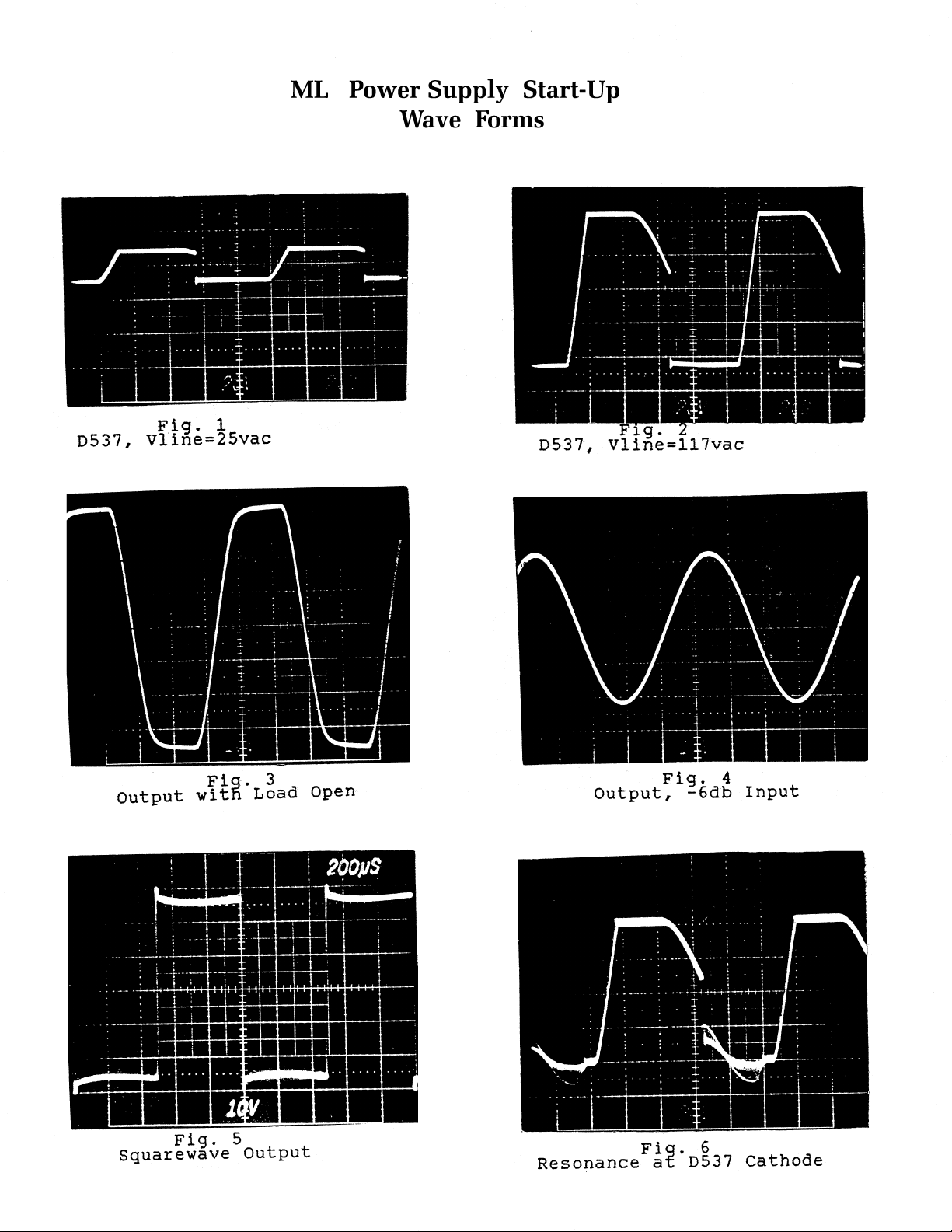
with Fig. 1 (As of 9/99- picture available only as poor copy, see accompanying wave form pages- Ed.). The top part of the waveform should
be starting to break over and droop towards the centerline. Adjust R508 until the scope looks like the photo. Counterclockwise increases
droop.
Full Line Voltage
Bring the variac up to 117Vac within 5 seconds, making sure that droop increases with voltage. During this period, the supplies will turn on
and the presence of current may be noticed in the bottom of the waveform. Obtain the droop as shown in Fig. 2 (see above note regarding
waveform pictures-Ed.) by adjusting R508 so that it stops 10V (1/2 div) below centerline. NOTE: If there is a problem with shorted supplies, it
can be detected by the shape at the bottom of this waveform as the variac is increased. It will show as excessive ringing and may look similar
to the bottom of the waveform of Fig. 6. If this occurs, do not increase the variac to 117Vac and refer to the Service Manual.
Adjust Period
At this stage the period is set such that the bottom flat part of the waveform is 4usec/ wide, +or-0.2usec. This may cause the period to be about
10.5usec, which can be adjusted by connecting or omitting C503, 504, & 505 with the shorting bock JU502. As a shorting clip is added from
the board edge towards the interior,, the capacitance added to the oscillator increases, and the period will increase. Always turn the unit off
when adding or removing clips. Adjust the reset as above as necessary. The waveform should now be similar to Fig. 2. The period and droop
will be finalized below. Leave the unit on.
IMPORTANT! – Only a polyester or polypropylene capacitor may be used for the oscillator, which is used for temperature stability. If it
is necessary, change one of the caps to get a waveform like Fig. 2. However, the caps provided will usually be sufficient.
Power Amp Start-Up
Preparation
Check that the emitter jumpers connect the transistors to the outputs. P612A, 655A and 683A should be toward the rear panel and P602A
should be towards the edge of the board. Connect the loads and set their toggle switches toward the middle, open circuiting them. Set the rear
panel pot of a power amp (ML/P) to be fully on. Set the 35MHz scope to 10/div. @ 200usec/div.
Continuity Test
With the DVM check that there is a short circuit between the grounding screw and the rear panel. The grounding screw is between Q824 and
Q808, and its washer must be touching the board. If an open circuit is measured, check that the screw hole in the heat sink is not anodized. It
is crucial that this connection is made.
Adjust Bias
With the loads open and the DVM on the 200mV DC scale, adjust R652 so that 8.5mV (+ or – 0.5mV) appears between the emitters of Q808
and Q824. (The emitter is the leftmost pin on TIP33 and TIP34). This voltage will increase as the unit warms up, and 8.5mVis recommended
when the unit is cool. For a stereo amp, repeat this procedure with R711, Q759 and Q783. For a mono amp, check above Q’s to see if base
connections have been made. Usually, a smaller voltage will appear between the left channel emitters of a mono power amp.
Load Tests
Open Circuit Test
Set the voltmeter to 30V full scale. Set the 35MHz scope to 10 div @ 200usec/div. Connect a 1kHz signal from the oscillator into the Stereo
Line Out (stereo), Right Line Out (mono), or Line In (power amp ML/P). This jack is next to the output jack on the right. Use a mono-tostereo adapter from the oscillator. With the loads open circuited, look at the output signal on each output jack with the 35MHz scope. The
waveform should look sinusoidal at low input levels (-16dB) and distorted at high input levels
Page 17

Open Circuit Test (contd.)
(-6dB). See Fig. 3 for a distorted signal. (See note regarding waveforms above. –Ed.) For a power amp (ML/P), check that turning down the
rear panel pot reduces the output to zero on each channel. Return the pot to fully on. Set the oscillator to be a –6dB, 1kHz signal. With both
loads set to 8 ohms, adjust R688A so that the output voltage from the left jack (R Channel) is 14.5Vrms, as indicated by the VOM. The output
should be a clean sine wave, as shown in Fig. 4 (see note above). The line current should be about 1.2A. Change the input signal to a square
wave and compare output with Fig.5. For a stereo unit, adjust R697 to obtain the same sine wave rms output voltage for the right output jack
(L Channel). Change the input to a square wave and check the output. For a mono unit, check that the output jumpers are connected by
viewing the signal on the right output jack, which should be the same as the left jack.
Resonance Check
With the loads at 8 ohms and a sine wave input, raise the input signal to 0dB and note that line current is 2A, which should send the output into
the rails. View the cathode of D537 with the 100MHz scope as mentioned above (Scope Setup). The S-curve due to resonant current should
stop about 0.5usec (deadtime) before the waveform rises, as shown in Fig.6. If this is not the case, the period must be readjusted (see Adjust
Period). The condition of not enough deadtime may be the result of a transformer core having too high a relative permeability, which makes
the magnetizing inductance too high. Therefore, the magnetizing current will be less, which will increase the ring-up time. In this case, add
more capacitance. If there is too much deadtime, decrease the period by decreasing capacitance, making sure deadtime is still at a safe level.
This will increase the operating frequency to a value closer to the transformer deign goal. Once the period is adjusted with respect to the
resonance, adjust the droop to 10V above zero. Securely glue the pot (R508).
Thermal Lift
With both sides connected to 8 ohms, set the input signal to be a –6dB, 1kHz sine wave. While observing the left output signal, short JU789
from the left outside pin to the middle with a screwdriver. After a short delay the output should go to zero. For a stereo unit, cycle the power
switch, waiting 2 seconds before turning back on. Repeat the above procedure for the right side output, this time shorting the right side of
JU789 to the center pin.
Overload
NOTE: in the following sections the amp will automatically shut off. To reset, the power switch must be turned off for 2 seconds before the
unit can again produce output when turned on.
Stereo- With the input set to 0dB, set both loads to 4 ohms. The amp should not trip off. Switch in the 8.2ohm load on the left side. The
automatic shutoff circuit should force the output to go to zero after a short delay (a few seconds max.). If this does not happen, R777 must be
adjusted. This component must be decreased in value (from 470 ohms) by paralleling it with either a 2.2k or a 1k resistor. If the unit still stays
on, R777 must be changed to a lower value. Settle on the value that trips first. Repeat the shutoff test on the right side, switching in the
8.2ohm load and adjusting R761 if necessary. Remove the 8.2 ohm load and switch the load box to 8 ohm on either side.
Mono-Remove the right jack from the unit and plug it into the left side of the load box, paralleling the loads. With a 0dB sine wave input and
both loads set to 4 ohms, the unit should not trip off. Switch in the 8.2ohm load. The output should go to zero after a short delay. If this does
not happen, R777 should be adjusted. This may be adjusted by paralleling a 2.2k or a 1k resistor, as noted in the above section. If this doesn’t
work, change R777 to a lower value, settling on the value that trips first. Switch loads back to 8 ohms and connect each output jack to a load.
Page 18
Page 19

Microamplifier Series-Lead
Standard Preamp Turn-On Procedure
GK Document #420-0073-A
Preamp Board # 206-0073-D- ML/S board
Model #’s- ML120S, ML260S-All Options
5/18/90 Rev. 9/15/99-SW
NOTE: Italics refer to stereo power units.
SETUP
Power switch off- Connect power cord.
1) Connect power 3-pin connector from power amp to P1 on board. Colors should read (L-R): Black, Violet, Brown. P1 is furthest to the
back.
2) Connect signal 3-pin connector from power amp to P2. These colors should read (L-R): White, Black, Red. P2 is furthest the front.
3) Connect outputs to load box- Left to Load A, Right to Load B.
4) Resistance loads open (switch in center).
5) Load box to scope-B and AC-VM.
6) Set scope switch on load box to look at load A (down).
7) Probe (1:1) to scope-A and DVM. (No gnd lead required).
8) Connect oscillator to unit.
9) Set oscillator on 100Hz sine wave @ 1.6Vrms (+4dBV).
10) DVM on 20V DC range.
11) AC Voltmeter on 30V range.
12) Scope-A on 5V/cm, scope-B on 10V/cm.
13) Scope sweep on 1ms/cm, scope trigger on A.
14) Output level to 0, switches out.
15) Boost, shape, gain, lead master to 0.
16) Clean volume, tones to 10.
INPUT SETUP AND LEAD CHANNEL TEST
1) Turn on power switch- clean channel LED only should light.
2) Engage channel switch- lead channel LED only should light.
3) Look at U1/1 with probe. Adjust R5 so that signal hits the rails evenly on both sides. Signal should be about 22Vp-p.
4) Look at drain of Q48 (square pad-J113): +7.3VDC.
5) Adjust R63 (1k trim) for 4.0-4.5VDC on drain of Q59 (J113).
6) Adjust R86 (1k trim) for 5.8-6.2VDC on drain of Q69 (J113).
7) Increase gain to 10 and watch the signal become a square wave- it should clip fairly evenly on both sides and reach 9Vp-p.
8) Decrease oscillator level to –66dBV (.5mV).
9) Change DVM to AC (20V) scale.
10) Adjust R70 (50k trim) for 2VAC at drain of Q69.
CLEAN CHANNEL TEST
1) Change scope trigger to B.
2) Disengage channel switch so that clean channel LED lights.
3) Set oscillator to –46dBV (5mV) in at 100Hz.
4) Look at tip of Send jack (J2) with probe: 0.47Vrms.
5) Tip and ring of Line Out jack (J4) should be 0.92Vrms.
6) With output level at 0, there should be no output. Gradually increase output and it should hit the rails at about 1o’clock and =30Vrms.
7) Flip scope switch to look at load B (up) and see that it also is about 30Vrms, and hits the rails at about 1 o’clock.
8) Look at tip of Headphone Output jack (J5) and continue increasing the output level. Headphone output should hit the rails at about 4
o’clock (it actually may not hit the rails even when all the way up). It should be about 4.4Vrms.
9) Repeat 8) looking at ring of headphone jack.
TONE CONTROLS TEST
1) Set all large knobs to center (12 o’clock), switches out.
2) Set scope-B to 2V/cm @ 1ms/cm.
3) Set oscillator to 100Hz square wave at –46dBV.
4) Look at output, compare to Fig. 1.
5) One at a time, turn tone control knobs and compare outputs, resetting after finishing:
A) Treble to 10- Fig.2; treble to 0- Fig.3.
Page 20

B) Hi-mid to 10- Fig.4; hi-mid to 0- Fig.5.
C) Lo-mid to 10- Fig.6; lo-mid to 0- Fig.7.
D) Bass to 10- Fig.8; bass to 0- Fig.9.
BOOST / SHAPE TEST
1) Engage Channel select switch to go to lead channel.
2) Change scope-B to 5V/cm @1ms/cm.
3) Increase shape to 10- compare to Fig.11.
4) Increase boost to 10- compare to Fig.12.
FOOTSWITCH TEST
1) Connect RFG2 to footswitch jack (J6).
2) Engage switches on RFG2 so that both LEDs are lit. Lead channel LED should also be lit.
3) Output should look like Fig.12.
4) Disengage boost switch on RFG2-compare to Fig.11.
5) Disengage channel switch on RFG2- compare to Fig.1 (change scope range to 2V/cm, if necessary. Clean channel LED should light.
6) Remove footswitch.
RETURN STEREO/MONO TEST
1) Set AC-VM to 10V scale.
2) Set oscillator to 100Hz sine wave at –26dBV (50mV).
3) Insert plug from oscillator halfway into return jack (J3).
4) Set output level to 10. R Channel = 7.1Vrms (stereo). 4V for mono amp. Scope switch should be set to load B.
5) Push in stereo/mono switch (S2); signal goes away.
6) Disengage stereo/mono switch; signal comes back.
7) Push plug in the rest of the way. Signal disappears again on stereo unit, measures 4Vrms on mono unit.
8) Flip scope switch to down- L Output = 7.4vrms.
9) Engage stereo/mono switch: L Channel output = 7Vrms.
NOISE TEST
1) Remove oscillator input.
2) Turn all front panel knobs to 10, switches out.
3) Connect speaker to Left Output (switches out) and listen for noise, should be smooth with no crackling.
4) Change AC-VM range to 1V.
5) Noise should measure less than: 400mVrms, 500mV-mono.
6) Change speaker to Right Output (switch up) and listen for noise.
7) Also change scope switch (up) to measure noise in R Channel as < 400mVrms.
8) Engage channel select switch to change to lead channel.
9) Noise in speaker should be smooth, with no crackling and should measure: 250mVrms, 400mVrms-mono (on AC-VM).
RETURN KNOBS TO ZERO- READY FOR BURN-IN
Page 21

Microamplifier Series-Lead
Effects Preamp Turn-On Procedure
GK Document # 420-0063 –A
Model #’s: ML120E, ML260E- All options
Board #: 206-0063-E (ML/E preamp)
5/18/90 Rev.9/15/99-SW
NOTE: Italics refer to stereo power units.
SETUP
1) Power switch off- Connect power cord.
2) Connect power 3-pin connector from power amp to P1 on board. The colors should read (bottom-top): Black, Violet, and Brown. P1 is
closest to front.
3) Connect signal 3-pin connector from power amp to P2 on board. The colors should read (bottom-top): White, Black, and Red. The colors
are clearly marked on the board for both connectors.
4) Connect outputs to load box- left to load-A, right to load-B.
5) Resistance loads open (switch in center).
6) Load box to scope-B and AC-VM.
7) Set scope switch on load box to look at load-A (down).
8) Probe (1:1) to scope-A and DVM. (No gnd lead required.)
9) Connect oscillator to input.
10) Oscillator on 100Hz sine wave @ 1.6Vrms (+4dBV).
11) DVM on 20V DC range.
12) AC-VM on 30V range.
13) Scope-A on 5V/cm, Scope-B on 10V/cm.
14) Scope sweep on 1ms/cm, trigger on A.
15) Boost, gain, lead master, shape, and output level to 0.
16) Clean volume, tones 10, all switches out.
17) Reverb, rate, and depth to 0.
INPUT SETUP AND LEAD CHANNEL TEST
1) Turn on power switch- clean channel LED only should light.
2) Engage channel switch- lead channel LED only should light.
3) Look at U1/1 with probe. Adjust R5 (1k trim pot) until signal hits the rails on both sides evenly. Should be about 22Vp-p.
4) Look at drain of Q50 (square pad-J113): +7.3Vdc.
5) Adjust R67 for 4.0-4.5Vdc on drain of Q67 (J113).
6) Adjust R87 for 5.8-6.2Vdc on drain of Q78 (J113).
7) Increase gain to 10 and watch the signal become a square wave- it should clip evenly and reach about 9Vp-p.
8) Decrease oscillator level to –66dBV (.5mVrms).
9) Change DVM to AC (20V) scale.
10) Adjust R86 (50k trim) for 2.0Vac at drain of Q78.
CLEAN CHANNEL TEST
1) Change scope-A to .5V/cm.
2) Disengage channel switch so that the clean channel LED lights.
3) Set oscillator to –46dBV (5mV) at 100Hz.
4) Look at tip of send jack (J7) with probe: 0.47Vrms.
5) Engage compressor. Send = 0.94Vrms. Disengage compressor. (Monitor both signals to make sure they are clean sine waves.
6) Change scope trigger to B.
7) With output level at 0, there should be no output. Gradually increase output level and it should hit the rails at about 1 o’clock and =
30Vrms.
8) Flip scope switch to load B (up) and see that it also is 30Vrms and hits the rails at 1 o’clock on output level.
9) Look at tip of headphone jack (J5) and continue increasing output level. Headphone output should be about 4.4Vrms with output level at
max (may not even hit rails with output all the way up).
10) Repeat 9) looking at ring of headphone jack.
TONE CONTROLS TEST
1) Set front panel knobs to center (12 o’clock) except: boost, shape reverb, rate and depth to 0, gain to 10, switches out.
2) Set scope-B to 2V/cm @1ms/cm.
3) Set oscillator to 100Hz square wave at –46dBV.
4) Look at output, compare to Fig. 1.
Page 22

5) One at a time, turn control knobs and compare outputs to figures below (resetting after finishing):
A) Treble to 10 –Fig.2; treble to 0- Fig. 3.
B) Hi-mid to 10- Fig.4; hi-mid to 0- Fig.5.
C) Lo-mid to 10- Fig.6; lo-mid to 0- Fig.7
D) Bass to 10- Fig.8; bass to 0- Fig.9.
BOOST AND SHAPE TEST
1) Engage channel select switch to back to lead channel.
2) Change scope-B to 5V/cm (still 1ms/cm).
3) With boost and shape on 0, compare to Fig.10.
4) Increase shape to 10- compare output to Fig. 11.
5) Increase boost to 10- compare output to Fig. 12.
CHORUS AND REVERB TEST
1) Return to clean channel (w/ channel select). Set output level to 0.
2) Set oscillator to –6dBV sine wave @ 100Hz.
3) Adjust R342 for no clipping @ U21/4.
4) Set oscillator to –26dBV square wave @100Hz.
5) Change scope trigger to A and scope-A to .5V/cm range.
6) Look at balanced out-R (J3) pin 3 (center).
7) Turn reverb knob to 10- see bumps in output as in Fig. 13.
8) Move frequency dial on oscillator back and forth around 100Hz- see signal bounce a little then settle.
9) Repeat 8) for each: Bal. Out-R (J3) pin 2 (left), Bal. Out-L (J4) pin 3 and pin 2.
10) Return reverb knob to 0.
11) Engage chorus switch with rate and depth of 0.
12) Look at Bal. Out-R pin 3, compare to Fig. 14.
13) It should have a small spike that moves back and forth approx. 1 div. at the rate of once every 2-3 sec.
14) Increase rate to max. Spike travel should speed up to about once every .7 seconds. Reset rate to 0.
15) Increase depth to max. Spike should travel about 5 full divisions. Reset depth to 0.
16) Look at Bal. Out-R pin 2 (left) and compare to Fig. 14.
17) Engage stereo/mono switch (S5). Spike gets bigger (Fig.15).
18) Look at Bal. Out-L pin 3 (center)- compare to Fig. 14.
19) Disengage stereo/mono switch- compare to Fig. 15.
20) Move probe to Bal. Out-L pin 2- compare to Fig. 15.
21) Set DVM to ohms scale.
22) Look at Bal. Out-R pin 1 (right) and see reading on DVM (number not important).
23) Engage gnd lift switch (S4) and see reading change to 1-open.
24) Repeat for Bal. Out-L.
FOOTSWITCH TEST
1) Set oscillator to –46dBV square wave @100Hz.
2) Set scope-B to 5V/cm, trigger on B.
3) Set output level to 12 o’clock.
4) Connect RFG4 to footswitch jack (J8) using 5-pin DIN cord.
5) Make sure both channel select and chorus switches are in, and boost and reverb pots at max.
6) Engage switches on RFG4 so that all LEDs are lit. Lead channel, chorus LEDs on front panel should be lit.
7) Output should look like Fig. 16.
8) Disengage reverb switch on RFG4- reverb bumps should disappear.
9) Disengage chorus switch. Chorus LED should go off and chorus spikes should go away.
10) Disengage boost switch. Compare to Fig. 11.
11) Disengage channel switch. Compare to Fig. 1. (Change scope range to 2V/cm, if necessary.) Clean channel LED should light.
12) Engage compressor switch on RFG4- see output increase.
13) Remove footswitch. Set front panel switches out and reverb to 0.
Page 23

RETURN AND STEREO AUX IN TEST
1) Set AC-VM to 10V scale.
2) Set oscillator to 100Hz sine wave @ -26dBV (50mV).
3) Insert plug from oscillator into return jack (J6).
4) Set output level to 10: R channel output = 5.5Vrms.
5) Insert plug from oscillator halfway into stereo aux in jack (J5). R output = 15Vrms, 8Vrms-mono.
6) Push plug all the rest of the way in- signal goes away on stereo unit and = 7Vrms on mono unit.
7) Flip scope switch (down) to look at L output = 15Vrms.
NOISE TEST
1) Remove oscillator input.
2) Turn all front panel knobs to 10, switches out.
3) Connect speaker to L output (switch down) and listen for noise. Sound should be smooth w/ no crackling.
4) Change AC-VM to 1V range.
5) Noise should measure less than: 400mVrms, 500mV-mono.
6) Change speaker to R output (up) and listen. Sound should be smooth.
7) Also change scope switch (up) to measure noise in R channel as less than 400mVrms.
8) Engage compressor switch- noise should measure less than 600mVrms (400mVrms-mono) and be smooth.
9) Engage channel select switch to change to lead channel.
10) Noise in speaker should again be smooth and measure: 250mVrms, 400mVrms-mono.
11) Set AC-VM to 30mV range.
12) Set all knobs to zero except output level and reverb to 10, chorus switch in (may be a slight pop)- noise < 20mVrms.
RETURN KNOBS TO ZERO, SWITCHES OUT- READY FOR BURN-IN.
Page 24

Page 25

Page 26

Page 27

Page 28

Page 29

Page 30

Page 31

Page 32

Page 33

Page 34

Page 35

Page 36

Page 37

Page 38

Page 39

Page 40

Page 41

Page 42

Page 43

Page 44

Page 45

Page 46

Page 47

Page 48

Page 49

Page 50

Page 51

Page 52

Page 53

ML120S INDENTED BILL OF MATERIALS
NOTE: Level 1 refers to main assembly parts.
Addtl. Note This B.O.M. will work for all ML/S options.
LVL PART# DESCRIPTION QTY REF. DESIG.
Level 2 refers to board level components.
Main assembly numbers are in bold face, while
commonly used parts are italicized.
See ML/E BOM for power supply parts.
1 010-0012-0 MPSA06 NPN 80V 500MA TO-92 2
1 011-4181-0 BUK456 N-MOSFET 800V 3A TO-220 2
1 012-0084-0 TIP 33CFP NPN 100V 10A TO218 2
1 012-1085-0 TIP 34CFP,PNP,100V,10A,TO-218,PECOR 2
1 014-0031-0 LM7815 +15V REG 1A TO-220 1
1 014-1032-0 LM7915 -15V REG 1A TO-220 1
1 021-1124-0 BYW29-200,RECT-FAST,8A,200V,25NS,TO-220 2
1 022-2079-0 SNRA130K20 MOV,130V 1
1 032-3104-0 CAP,METALIZED POLYESTER,104,5%,63V 1
1 082-0047-0 SPEAKER,6.5",80W,Z=16 PYLE-LEAD 2
1 091-0018-0 FUSE, 2.5A,250V,5MM X 20MM,SLB 1
1 093-0035-0 HOUSING,4X.156,FEMALE 22GA,LOCK 1
1 093-0066-0 SHUNT .1,TIN 2
1 093-0067-0 SHUNT .2,TIN 3
1 094-0018-0 SOLDER LUG,#4 1
1 094-0041-0 RECEPTICAL AC,LINE FILT 02BEEG3H,2A,FUSE 1
1 095-0005-0 POWER CORD,117V PLUG,DETACH 1
1 100-0012-0 GROMIT,3/16 X.100 1
1 100-0014-0 INSULATOR/SHIELD,2XTO-220 1
1 100-0020-0 BUMPER,ROUND RUBBER,1/2"X.14" 2
1 100-0027-0 BUTTON,ROUND BLACK CAP - PUSH SWITCH 1
1 100-0037-0 HEAT CLIP,TO-98 2
1 100-0038-0 BUMPER,ROUND RUBBER,5/8X5/16 2
1 100-0061-0 CLAMP,TO-220,”VDE” 2
1 100-0069-0 CLAMP-TO220 4
1 100-0076-0 FOOT,RUBBER,ROUND,5/8DIA. X 5/8" 2
1 100-0081-0 CORNER,CHEVRON,PLASTIC,WOOD CABS 1
1 100-0096-0 KNOB,BLUE,6X15MM SPLINE SHAFT 4
Page 54

LVL PART# DESCRIPTION QTY REF. DESIG.
1 100-0099-0 KNOB,RED,6X15MM SPLINE SHAFT 4
1 111-0030-0 SEE 111-8030-0 8
1 111-0061-0 BOLT 4-40 3/8 PHP CAD 2
1 111-0084-0 BOLT 4-40 1/2 PHP-WASHER CAD 5
1 111-3061-0 SEE 111-8061-0 3
1 111-6001-0 NUT 4-40 KEP SMALL 2
1 111-7021-0 WASHER #4 FLAT CAD 4
1 112-0084-0 SEE 112-0104-0 6
1 112-1080-0 BOLT 6-32 1/2 FHP 82^ B.O. 2
1 112-3040-0 SCREW 6AB 1/4 PHP B.O. 17
1 112-3121-0 SCREW 6AB 3/4 PHP CAD 6
1 112-4060-0 SCREW 6AB 3/8 FHP 82' B.O. 24
1 112-4081-0 SCREW 6AB 1/2 FHP 82^ CAD 6
1 112-7001-0 WASHER #6 FLAT CAD 2
1 113-1121-0 SEE 113-1141-0 2
1 113-8060-0 RT-BOLT 8-32 3/8 PHP B.O. 8
1 114-0080-0 BOLT 10-32 1/2 PHP B.O. 2
1 130-0004-0 OVERLAY,206 GRILL 1
1 130-0008-D INSULATOR,THERMO-STRIP,MICRO POWERAMP 1
1 130-0012-0 MICRO LEAD S FRONT PANEL OVERLAY 1
1 130-0018-0 MICRO LEAD 120S REAR PANEL OVERLAY 1
1 130-0492-A MICRO SERIES HEAT SINK 120W 1
1 132-0495-A MICRO LEAD 206 BAFFLE 1
2 120-0011-0 STEEL,18 GAUGE JET COAT,.048 320
1 132-0496-A MICRO LEAD 206 BACK 1
2 120-0011-0 STEEL,18 GAUGE JET COAT,.048 320
1 132-0497-A MICRO LEAD 206 GRILL 1
2 120-0011-0 STEEL,18 GAUGE JET COAT,.048 192
1 132-0498-A MICRO LEAD 206 RIGHT SIDE 1
2 114-6076-0 NUT 10-32 PRESS FOR ALUM. 1
2 120-0005-0 ALUM .100 104
1 132-0499-A MICRO LEAD 206 LEFT SIDE 1
2 114-6076-0 NUT 10-32 PRESS FOR ALUM. 1
Page 55

LVL PART# DESCRIPTION QTY REF. DESIG.
2 120-0005-0 ALUM .100 104
1 132-0521-0 MICRO LEAD S FRONT PANEL 1
2 120-0011-0 STEEL,18 GAUGE JET COAT,.048 48
1 132-0522-0 MS-S REAR PANEL 1
2 120-0011-0 STEEL,18 GAUGE JET COAT,.048 48
1 132-0525-E MICRO SERIES SUPPLY SHEILD 1
2 120-0016-0 STEEL,24 GA,JET COAT,.024 66
1 132-0537-0 MICRO COMBO HANDLE PLATE 1
2 120-0012-0 STEEL,20 GAUGE JET COAT,.036 23
1 132-0540-A MICRO SERIES INPUT SHIELD 1
2 120-0016-0 STEEL,24 GA,JET COAT,.024 4
1 132-0543-A 206 BRACE 1
2 120-0011-0 STEEL,18 GAUGE JET COAT,.048 87
1 150-0019-0 BAG,POLY 18X24XC [2 MIL.] 1
1 160-0000-0 MANUAL,MICRO SERIES 1
1 206-0071-E MICRO SERIES POWER SUPPLY 1
1 206-0073-D MICRO LEAD-S PREAMP 1
2 001-1030-0 LF353N DUAL JFET OP AMP 4 U1,U4,U5,U6
2 001-1038-0 LM386 LOW VOLTAGE POWER AMP 2 U7,U8
2 001-3028-0 TL604 DUAL COMP ANALOG SWITCH 2 U2,U3
See ML/E BOM for parts list
2 010-0012-0 MPSA06 NPN 80V 500MA TO-92 1 Q35
2 010-1013-0 MPSA56 PNP 80V 500MA TO-92 1 Q26
2 010-2010-0 J113 N-JFET 35V 2MA TO-92 8 Q9,Q19,Q36,Q48,Q59,Q69,Q73,Q87
2 020-0024-0 1N4370 ZENER,2.4V,5%,400MW,DO-7 1 D96
2 020-0120-0 1N759A,ZENER,12V,5%,400MW,DO-35 2 D7,D8
2 020-1103-0 1N914 ,RECT-FAST,200MA,100V,4NS,DO-35 1 D25
2 025-0101-0 LED-GREEN,6MCD,80 DEG,T-1 2 D38,D67
2 030-0223-0 CAP,CERAMIC AXIAL,223,30%,16V 2 C64,C112
2 030-1103-0 CAP,CERAMIC AXIAL,103,30%,25V 2 C66,C122
2 030-2101-0 CAP,CERAMIC AXIAL,101,5%,50V 1 C12
2 030-2102-0 CAP,CERAMIC AXIAL,102,10%,50V 2 C30,C102
2 030-2104-0 CAP,CERAMIC AXIAL,104,10%,50V,XR7,.3" 8 C18,C32,C47,C90,C152,C153,C160
2 030-2222-0 CAP,CERAMIC AXIAL,222,10%,50V 2 C42,C60
Page 56

LVL PART# DESCRIPTION QTY REF. DESIG.
2 030-2224-0 CAP,CERAMIC AXIAL,224,20%,50V,XR7 2 C78,C82
2 030-2271-0 CAP,CERAMIC AXIAL,271,10%,50V 1 C118
2 030-2472-0 CAP,CERAMIC AXIAL,472,10%,50V 5 C55,C84,C108,C116,C117
2 030-2473-0 CAP,CERAMIC AXIAL XR7,473,10%,50V 2 C154,C162
2 030-2474-0 CAP,CERAMIC AXIAL Z5U,474,20%,50V 1 C33
2 031-1227-0 CAP,ELECTROLYTIC RADIAL,227,-10%+50%,25V 5 C1,C2,C126,C129,C130
2 031-2335-0 CAP,ELECTROLYTIC RADIAL,335,20%,50V 1 C26A
2 032-3104-0 CAP,METALIZED POLYESTER,104,5%,63V 2 C10,C71
2 032-3105-0 CAP,METALIZED POLYESTER,105,5%,63V 2 C16,C53
2 032-3473-0 CAP,METALIZED POLYESTER,473,5%,63V 1 C44A
2 038-0336-0 CAP,ELECTIOLYTIC AXIAL,336,20%,16V 14 C62,C74,C81,C97,C100,C123,C137,C138,
2 038-2335-0 CAP,ELECTROLITIC AXIAL TR 335,20% 25V 2 C22,C146
2 051-0101-0 RES,CARBON FILM,10 OHM,1/4W,5% 4 R155,R158,R163,R164
2 051-0221-0 RES,CARBON FILM,22 OHM,1/4W,5% 1 R94
2 051-1001-0 RES,CARBON FILM,100 OHM,1/4W,5% 1
2 051-1002-0 RES,CARBON FILM,1K OHM,1/4W,5% 13 R6,R40,R50,R75,R92,R103,R105,R121,
2 051-1004-0 RES,CARBON FILM,100K OHM,1/4W,5% 6 R15,R45,R76,R91,R133,R144
2 051-1005-0 RES,CARBON FILM,1M OHM,1/4W,5% 1 R13
2 051-1203-0 RES,CARBON FILM,12K OHM,1/4W,5% 13 R11,R20,R29,R33A,R44,R49,R66A,R80,R98
2 051-2202-0 RES,CARBON FILM,2.2K OHM,1/4W,5% 6 R54,R57,R69A,R107,R111,R148
2 051-2203-0 RES,CARBON FILM,22K OHM,1/4W,5% 9 R31,R32A,R34,R52,R56,R58,R72,R134,141
2 051-2204-0 RES,CARBON FILM,220K OHM,1/4W,5% 7 R21,R23,R39,R43,R93,R106,R109
2 051-3302-0 RES,CARBON FILM,3.3K OHM,1/4W,5% 2 R24,R83
2 051-3303-0 RES,CARBON FILM,33K OHM,1/4W,5% 3 R51,R149,R150
C143,C145,C156,C157,C165,C166
R131,R132,R139,R140,R147
R135,R142,R151,R159
2 051-3904-0 RES,CARBON FILM,390K OHM,1/4W,5% 2 R99,R101
2 051-4701-0 RES,CARBON FILM,470 OHM,1/4W,5% 4 R3,R4,R85,R128
2 051-4702-0 RES,CARBON FILM,4.7K OHM,1/4W,5% 2 R41,R89
2 051-4703-0 RES,CARBON FILM,47K OHM,1/4W,5% 1 R110
2 051-4704-0 RES,CARBON FILM,470K OHM,1/4W,5% 2 R65,R68
2 051-5602-0 RES,CARBON FILM,5.6K OHM,1/4W,5% 5 R114,R119,R120,R124,R127
2 051-5603-0 RES,CARBON FILM,56K OHM,1/4W,5% 1 R88
Page 57

LVL PART# DESCRIPTION QTY REF. DESIG.
2 052-0000-0 RES,METAL WIRE, 0 OHM,1/4W,1% 1 R113
2 070-0501-0 POT,2X50KB,9MM,PLAST KNURL 14MM,.05W 2 R28,R136-gain, master
2 070-0505-0 POT,50K LIN,MINI POT 1 R17- boost
2 070-0506-0 POT,50KA,9MM,PLASTIC KNURL 14MM,.05W 2 R46,R77- A and B volume pots
2 070-0508-0 POT,1K TRIM,6MM,SLOT,.3W 3 R5,R63,R86
2 070-0510-0 POT,50K TRIM,6MM,SLOT,.3W 1 R70
2 070-0511-0 POT,10K LINEAR,MINI POT 1 R61- shape
2 070-0514-0 POT,50KB,LINEAR,9MM,METAL KNURL 9MM,.1 4 R95,R104,R115,R125-all EQ pots
2 090-0012-0 SWITCH,MINI PP,DPDT,.1A BRK/MAKE,PC TER 2 S1,S2-all switches
2 092-0075-0 JACK S2-BBB,1/4",S-TIP,S-RING,PC TERM 5 J1,J3,J4,J5,J6- all other jacks
2 092-0076-0 JACK S2-BNB,1/4",S-TIP,PC TERM 1 J2- send jack
2 093-0028-0 HEADER,3X.156,MALE,LOCK 2 P1,P2
2 100-0060-0 HOLDER,LED RIGHT ANGLE MOUNT 2 D38,D67
2 145-0073-0 MICRO LEAD-S PREAMP BOARD 1
1 206-0074-D MICRO LEAD HEAD, 120W MONO POWER AMP 1
2 001-1030-0 LF353N DUAL JFET OP AMP 2
2 001-1185-0 LM324N,QUAD OP-AMP,BIPOLAR,LOW POWER 2
2 010-0012-0 MPSA06 NPN 80V 500MA TO-92 4
2 010-1013-0 MPSA56 PNP 80V 500MA TO-92 3
2 011-0023-0 TIP29C NPN 100V 1A TO-220 FP 1
2 011-1035-0 TIP30C PNP 100V 1A TO-220 2
2 020-0050-0 1N751,ZENER,5V,10%,400MW,DO-35 2
2 020-1103-0 1N914 ,RECT-FAST,200MA,100V,4NS,DO-35 3
2 020-2105-0 1N4002,RECT,1A,150V,DO-41 5
2 030-1103-0 CAP,CERAMIC AXIAL,103,30%,25V 2
2 030-2101-0 CAP,CERAMIC AXIAL,101,5%,50V 2
2 030-2104-0 CAP,CERAMIC AXIAL,104,10%,50V,XR7,.3" 3
2 030-2105-0 CAP,CERAMIC AXIEL,105,20%,50V 2
2 030-2271-0 CAP,CERAMIC AXIAL,271,10%,50V 1
2 030-2470-0 CAP,CERAMIC AXIAL,47,5%,50V 1
2 030-2474-0 CAP,CERAMIC AXIAL Z5U,474,20%,50V 1
2 031-1227-0 CAP,ELECTROLYTIC RADIAL,227,-10%+50%,25V 2
2 038-0106-0 CAP,ELECTROLITIC AXIAL TR,106,20%,16V 2
Page 58

LVL PART# DESCRIPTION QTY REF. DESIG.
2 038-0336-0 CAP,ELECTIOLYTIC AXIAL,336,20%,16V 3
2 038-2108-0 CAP,ELECTROLYTIC AXIAL,108,-10%,50V 4
2 038-2335-0 CAP,ELECTROLITIC AXIAL TR 335,20% 25V 2
2 051-0221-0 RES,CARBON FILM,22 OHM,1/4W,5% 1
2 051-1001-0 RES,CARBON FILM,100 OHM,1/4W,5% 3
2 051-1002-0 RES,CARBON FILM,1K OHM,1/4W,5% 5
2 051-1004-0 RES,CARBON FILM,100K OHM,1/4W,5% 1
2 051-1005-0 RES,CARBON FILM,1M OHM,1/4W,5% 3
2 051-1203-0 RES,CARBON FILM,12K OHM,1/4W,5% 6
2 051-2202-0 RES,CARBON FILM,2.2K OHM,1/4W,5% 2
2 051-2203-0 RES,CARBON FILM,22K OHM,1/4W,5% 6
2 051-2204-0 RES,CARBON FILM,220K OHM,1/4W,5% 1
2 051-2205-0 RES,CARBON FILM,2.2M OHM,1/4W,5% 1
2 051-3302-0 RES,CARBON FILM,3.3K OHM,1/4W,5% 5
2 051-3303-0 RES,CARBON FILM,33K OHM,1/4W,5% 2
2 051-4302-0 RES,CARBON FILM,4.3K OHM,1/4W,5% 1
2 051-4701-0 RES,CARBON FILM,470 OHM,1/4W,5% 7
2 051-4702-0 RES,CARBON FILM,4.7K OHM,1/4W,5% 2
2 051-4703-0 RES,CARBON FILM,47K OHM,1/4W,5% 5
2 051-4704-0 RES,CARBON FILM,470K OHM,1/4W,5% 2
2 051-5602-0 RES,CARBON FILM,5.6K OHM,1/4W,5% 2
2 051-5603-0 RES,CARBON FILM,56K OHM,1/4W,5% 1
2 051-6802-0 RES,CARBON FILM,6.8K OHM,1/4W,5% 3
2 052-0000-0 RES,METAL WIRE, 0 OHM,1/4W,1% 7
2 052-1213-0 RES,METAL FILM,12.1K OHM,1/4W,1% 3
2 052-4703-0 RES,METAL FILM,47K OHM,1/4W,1% 4
2 054-2702-0 RES,CARBON FILM,2.7K OHM,1W,5% 2
2 056-.330-0 RES,CERAMIC WW,.33 OHM,5W,10% 5
2 056-0500-0 RES,CERAMIC WW,5 OHM,5W,10% 1
2 070-0508-0 POT,1K TRIM,6MM,SLOT,.3W 1
2 070-0510-0 POT,50K TRIM,6MM,SLOT,.3W 1
2 092-0075-0 JACK S2-BBB,1/4",S-TIP,S-RING,PC TERM 1
2 092-0076-0 JACK S2-BNB,1/4",S-TIP,PC TERM 2
Page 59

LVL PART# DESCRIPTION QTY REF. DESIG.
2 093-0030-0 HEADER,3X.1,MALE 1
2 093-0087-0 HEADER,6X.156,MALE RIGHT ANGLE LOCK 1
2 145-0064-0 MICRO SEIES, STEREO POWER AMP BOARD 1
1 602-0007-0 FORMS,WARRANTY CARDS 1
Page 60

ML260E INDENTED BILL OF MATERIALS
NOTE: Level 1 refers to main assembly parts
NOTE: This B.O.M. will work for all ML/E options.
LVL. PART# DESCRIPTION QTY REF. DESIG.
Level 2 refers to board level parts.
Main assembly numbers are in bold face, while
commonly needed parts are italicized
1 010-0012-0 MPSA06 NPN 80V 500MA TO-92 4
1 011-4181-0 BUK456 N-MOSFET 800V 3A TO-220 2
1 012-0085-0 TIP-35CFP NPN 100V 25A TO218 2
1 012-1086-0 TIP 36CFP,PNP,100V,25A,TO-218,PECOR 2
1 014-0031-0 LM7815 +15V REG 1A TO-220 1
1 014-1032-0 LM7915 -15V REG 1A TO-220 1
1 021-1124-0 BYW29-200,RECT-FAST,8A,200V,25NS,TO-220 2
1 022-2079-0 SNRA130K20 MOV,130V 1
1 032-3104-0 CAP,METALIZED POLYESTER,104,5%,63V 1
1 082-0047-0 SPEAKER,6.5",80W,Z=16 PYLE-LEAD 2
1 091-0012-0 FUSE,3.15 250V 5X20MM SLB 2
1 092-0064-0 Q-CON, .25 TAB,18-22GA,INSULATED 4
1 093-0032-0 HOUSING,3X.156,FEMALE 22GA,LOCK 2
1 093-0035-0 HOUSING,4X.156,FEMALE 22GA,LOCK 1
1 093-0066-0 SHUNT .1,TIN 1
1 093-0067-0 SHUNT .2,TIN 1
1 094-0018-0 SOLDER LUG,#4 1
1 094-0041-0 RECEPTICAL AC,LINE FILT 02BEEG3H,2A,FUSE 1
1 095-0005-0 POWER CORD,117V PLUG,DETACH 1
1 100-0012-0 GROMIT,3/16 X.100 2
1 100-0014-0 INSULATOR/SHIELD,2XTO-220 1
1 100-0020-0 BUMPER,ROUND RUBBER,1/2"X.14" 2
1 100-0027-0 BUTTON,ROUND BLACK CAP - PUSH SWITCH 1
1 100-0037-0 HEAT CLIP,TO-98 4
1 100-0038-0 BUMPER,ROUND RUBBER,5/8X5/16 1
1 100-0061-0 CLAMP,TO-220,”VDE” 2
1 100-0069-0 CLAMP-TO220 4
1 100-0076-0 FOOT,RUBBER,ROUND,5/8DIA. X 5/8" 2
Page 61

LVL PART# DESCRIPTION QTY REF. DESIG.
1 100-0080-0 HANDLE RUBBER,10" 1
1 100-0096-0 KNOB,BLUE,6X15MM SPLINE SHAFT 4
1 100-0098-0 KNOB,GRAY,6X15MM SPLINE SHAFT 1
1 100-0099-0 KNOB,RED,6X15MM SPLINE SHAFT 4
1 110-3040-0 SCREW 2AB 1/4 PHP B.O. 2
1 111-0061-0 BOLT 4-40 3/8 PHP CAD 2
1 111-0084-0 BOLT 4-40 1/2 PHP-WASHER CAD 5
1 111-3044-0 SCREW 4B 1/4 PHP-WASHER CAD 5
1 111-6001-0 NUT 4-40 KEP SMALL 2
1 111-7021-0 WASHER #4 FLAT CAD 4
1 111-8030-0 TR-BOLT 4-40 3/16 PHP B.O. 2
1 111-8061-0 TR-BOLT 4-40 3/8 PHP CAD 3
1 112-0104-0 BOLT 6-32 5/8 PHP CAD WITH EXT SIM WAS 6
1 112-3040-0 SCREW 6AB 1/4 PHP B.O. 2
1 112-3081-0 SCREW 6AB 1/2 PHP CAD 6
1 112-4081-0 SCREW 6AB 1/2 FHP 82^ CAD 3
1 112-7001-0 WASHER #6 FLAT CAD 2
1 112-8040-0 TR-BOLT 6-32 1\4 PHP B.O. 18
1 112-9060-0 TR-BOLT 6-32 3/8 FHP B.O. 23
1 113-1141-0 BOLT 8-32 7/8 FHP CAD 2
1 113-8060-0 RT-BOLT 8-32 3/8 PHP B.O. 8
1 114-0080-0 BOLT 10-32 1/2 PHP B.O. 2
1 114-1016-0 BOLT 10-32 1 OHP 82^ B.O. 2
1 115-7005-0 WASHER 3/8 FIBRE FLAT 8
1 115-7021-0 WASHER 3/8 INTERNAL CAD 3
1 130-0002-0 MICRO LEAD E FRONT PANEL OVERLAY 1
1 130-0003-0 MICRO LEAD E 2X60 REAR PNL OVERLAY 1
1 130-0004-0 OVERLAY,206 GRILL 1
1 130-0008-D INSULATOR,THERMO-STRIP,MICRO POWERAMP 1
1 130-0492-A MICRO SERIES HEAT SINK 120W 1
1 132-0493-A MICRO LEAD E FRONT PANEL 1
2 120-0011-0 STEEL,18 GAUGE JET COAT,.048 48
1 132-0494-A MS-E REAR PANEL 1
Page 62

LVL PART# DESCRIPTION QTY REF. DESIG.
2 120-0011-0 STEEL,18 GAUGE JET COAT,.048 48
1 132-0495-A MICRO LEAD 206 BAFFLE 1
2 120-0011-0 STEEL,18 GAUGE JET COAT,.048 320
1 132-0496-A MICRO LEAD 206 BACK 1
2 120-0011-0 STEEL,18 GAUGE JET COAT,.048 320
1 132-0497-A MICRO LEAD 206 GRILL 1
2 120-0011-0 STEEL,18 GAUGE JET COAT,.048 192
1 132-0498-A MICRO LEAD 206 RIGHT SIDE 1
2 114-6076-0 NUT 10-32 PRESS FOR ALUM. 1
2 120-0005-0 ALUM .100 104
1 132-0499-A MICRO LEAD 206 LEFT SIDE 1
2 114-6076-0 NUT 10-32 PRESS FOR ALUM. 1
2 120-0005-0 ALUM .100 104
1 132-0525-E MICRO SERIES SUPPLY SHEILD 1
2 120-0016-0 STEEL,24 GA,JET COAT,.024 66
1 132-0537-D MICRO COMBO HANDLE PLATE,”REV D” 1
2 120-0012-0 STEEL,20 GAUGE JET COAT,.036 27
1 132-0540-A MICRO SERIES INPUT SHEILD 1
2 120-0016-0 STEEL,24 GA,JET COAT,.024 4
1 132-0543-A 206 BRACE 1
2 120-0011-0 STEEL,18 GAUGE JET COAT,.048 87
1 150-0019-0 BAG,POLY 18X24XC [2 MIL.] 1
1 160-0000-0 MANUAL,MICRO SERIES 1
1 206-0063-E MICRO LEAD-E PREAMP 1
2 001-0001-0 MN3011 MULTI-TAP BBD 1 U21
2 001-0006-0 MN3007 1024 STAGE BBD 2 U22,24
2 001-1030-0 LF353N DUAL JFET OP AMP 12 U1,U7,U8,U10,U13,U15,U17,U18,U19
2 001-1038-0 LM386 LOW VOLTAGE POWER AMP 2 U11,12
2 001-1042-0 RC5532NB BI-POLAR OP-AMP 1 U4
U20,U27,U28
2 001-2044-0 MN3101 CLOCK GENERATOR/DRIVER 2 U23,25
2 001-2060-0 LM555CN TIMER 1 U26
2 001-3028-0 TL604 DUAL COMP ANALOG SWITCH 5 U2,3,9,16
Page 63

LVL PART# DESCRIPTION QTY REF. DESIG.
2 001-4043-0 NE571 DUAL COMPANDOR 2 U5,U14
2 010-0012-0 MPSA06 NPN 80V 500MA TO-92 1 Q36
2 010-1013-0 MPSA56 PNP 80V 500MA TO-92 1 Q30
2 010-2010-0 J113 N-JFET 35V 2MA TO-92 8 Q9,Q20,Q40,Q50,Q67,Q78,Q82,Q121
2 020-0024-0 1N4370 ZENER,2.4V,5%,400MW,DO-7 5 D92,D105,D107,D269,D271
2 020-0036-0 1N747A,ZENER,3.6V,5%,400MW,DO-35 2 D383,D385
2 020-0120-0 1N759A,ZENER,12V,5%,400MW,DO-35 2 D7,D8
2 020-1103-0 1N914 ,RECT-FAST,200MA,100V,4NS,DO-35 7 D28,D206,D208,D210,D212,D349,D368
2 025-0101-0 LED-GREEN,6MCD,80 DEG,T-1 3 D44,D88,D167
2 030-0223-0 CAP,CERAMIC AXIAL,223,30%,16V 2 C71,C148
2 030-1103-0 CAP,CERAMIC AXIAL,103,30%,25V 6 C62,C132,C161,C228,C231,C367
2 030-2101-0 CAP,CERAMIC AXIAL,101,5%,50V 5 C12,C112,C124,C239,C241
2 030-2102-0 CAP,CERAMIC AXIAL,102,10%,50V 8 C34,C142,C283,C284,C297,C298,C353,C370
2 030-2104-0 CAP,CERAMIC AXIAL,104,10%,50V,XR7,.3" 12 C16,C32,C41,C128,C183,C184,C195,C196,
2 030-2222-0 CAP,CERAMIC AXIAL,222,10%,50V 11 C42,C49,C254,C258,C266,C270,C276,C282,
2 030-2224-0 CAP,CERAMIC AXIAL,224,20%,50V,XR7 4 C75,C79,C177,C378
2 030-2271-0 CAP,CERAMIC AXIAL,271,10%,50V 9 C165,C256,C261,C267,C279,C292,C306,
2 030-2472-0 CAP,CERAMIC AXIAL,472,10%,50V 8 C45,C81,C140,C149,C162,C333,C340,C357
2 030-2473-0 CAP,CERAMIC AXIAL XR7,473,10%,50V 3 C186,C197,C209
2 030-2474-0 CAP,CERAMIC AXIAL Z5U,474,20%,50V 6 C23,C376,C389,C391,C398,C400
2 031-1227-0 CAP,ELECTROLYTIC RADIAL,227,-10%+50%,25V 8 C1,C2,C57,C65,C175,C350,C351,C369
2 032-3104-0 CAP,METALIZED POLYESTER,104,5%,63V 2 C10,C69
2 032-3105-0 CAP,METALIZED POLYESTER,105,5%,63V 2 C15,C59
2 032-3473-0 CAP,METALIZED POLYESTER,473,5%,63V 1 C46A
2 038-0106-0 CAP,ELECTROLITIC AXIAL TR,106,20%,16V 2 C97,C317
2 038-0336-0 CAP,ELECTIOLYTIC AXIAL,336,20%,16V 20 C60,C83,C86,C101,C125,C136,C137,C174,
C291,C296,C305,C310
C295,C309,C386
C373A,C381
C185,C188,C191,C192,C199,C200,C201,
C203,C237,C238,C403,C406
2 038-2335-0 CAP,ELECTROLITIC AXIAL TR 335,20% 25V 35 C25,C89A,C91,C95,C103,C106,C114,C115,
2 051-0101-0 RES,CARBON FILM,10 OHM,1/4W,5% 4 R187,R193,R198,R202
C117,C120,C126,C166,C168,C204,C205,
C218,C224,C225,C227,C229,C251,C252,
C262,C274,C281,C312,C314,C320,C334,
C343,C361,C362,C399,C404,C405
Page 64

LVL PART# DESCRIPTION QTY REF. DESIG.
2 051-0221-0 RES,CARBON FILM,22 OHM,1/4W,5% 3 R90,R352,R373
2 051-1001-0 RES,CARBON FILM,100 OHM,1/4W,5% 1 R22
2 051-1002-0 RES,CARBON FILM,1K OHM,1/4W,5% 15 R6,R47,R52,R84,R89,R109,R139,R144,R169,
2 051-1004-0 RES,CARBON FILM,100K OHM,1/4W,5% 26 R17,R39,R73,R94,R96,R99,R138,R253,R263
2 051-1005-0 RES,CARBON FILM,1M OHM,1/4W,5% 2 R13,R214
2 051-1203-0 RES,CARBON FILM,12K OHM,1/4W,5% 29 R11,R21,R31,R36A,R46,R51,R64,R85,R127,
2 051-1204-0 RES,CARBON FILM,120K OHM,1/4W,5% 7 R236,R249,R268,R321,R332,R335,R337
2 051-1504-0 RES,CARBON FILM,150K OHM,1/4W,5% 3 R272,R324,R325
2 051-2201-0 RES,CARBON FILM,220 OHM,1/4W,5% 1 R108
2 051-2202-0 RES,CARBON FILM,2.2K OHM,1/4W,5% 10 R58,R63,R77,R147,R151,R219,R311,R315,
2 051-2203-0 RES,CARBON FILM,22K OHM,1/4W,5% 27 R24,R30A,R33,R43,R48,R53,R70,R98,R102,
2 051-2204-0 RES,CARBON FILM,220K OHM,1/4W,5% 9 R19,R26,R29,R37,R146,R154,R158,R171,176
R217,R230,R316,R377,R401,R402
R264,R277,R293,R307,R328,R329,R336,
R338,R344,R345,R346,R358,R359,R364,
R366,R382,R387
R180,R181,R182,R194,R216,R234,R235,
R286,R299,R313,R318,R372,R388,R390,
R392,R393,R394,R395,R396,R397
R319,R380
R104,R116,R119,R123,R221,R222,R232,
R233,R250,R273,R287,R288,R301,R302,
R354,R355,R374,R375
2 051-2206-0 RES,CARBON FILM,22M OHM,1/4W,5% 2 R113,R226
2 051-2701-0 RES,CARBON FILM,270 OHM,1/4W,5% 2 R290,R304
2 051-3302-0 RES,CARBON FILM,3.3K OHM,1/4W,5% 3 R27,R80,R371
2 051-3303-0 RES,CARBON FILM,33K OHM,1/4W,5% 14 R56,R170,R179,R190,R242,R243,R246,R248,
2 051-3304-0 RES,CARBON FILM,330K OHM,1/4W,5% 1 R265
2 051-3904-0 RES,CARBON FILM,390K OHM,1/4W,5% 4 R145,R152,R245,R247
2 051-4302-0 RES,CARBON FILM,4.3K OHM,1/4W,5% 1 R213
2 051-4701-0 RES,CARBON FILM,470 OHM,1/4W,5% 6 R3,R4,R129,R130,R135,R379
2 051-4702-0 RES,CARBON FILM,4.7K OHM,1/4W,5% 5 R35,R100,R133,R289,R303
2 051-4703-0 RES,CARBON FILM,47K OHM,1/4W,5% 11 R111,R141,R215,R220,R223,R240,R244,
2 051-4704-0 RES,CARBON FILM,470K OHM,1/4W,5% 3 R72,R76,R207
2 051-5602-0 RES,CARBON FILM,5.6K OHM,1/4W,5% 13 R153,R156,R157,R159,R163,R164,R173,
2 051-5603-0 RES,CARBON FILM,56K OHM,1/4W,5% 10 R122,R211,R285,R300,R322,R323,R326,
R255,R260,R280,R294,R308,R384
R257,R259,R275,R278
R339,R347,R348,R360,R363,R365
R327,R330,R331
Page 65

LVL PART# DESCRIPTION QTY REF. DESIG.
2 052-0000-0 RES,METAL WIRE, 0 OHM,1/4W,1% 1 R150
2 070-0501-0 POT,2X50KB,9MM,PLAST KNURL 14MM,.05W 3 R38,R160,R189
2 070-0505-0 POT,50K LIN,MINI POT 3 R18,R172,R178-boost,rate,depth
2 070-0506-0 POT,50KA,9MM,PLASTIC KNURL 14MM,.05W 2 R61,R93lead,volume
2 070-0508-0 POT,1K TRIM,6MM,SLOT,.3W 3 R5,R66,R87
2 070-0510-0 POT,50K TRIM,6MM,SLOT,.3W 4 R68,R341,R342,R356
2 070-0511-0 POT,10K LINEAR,MINI POT 1 R74-shape
2 070-0514-0 POT,50KB,LINEAR,9MM,METAL KNURL 9MM,.1W 4 R110,R118,R131,R143- EQ pots
2 090-0012-0 SWITCH,MINI PP,DPDT,.1A BRK/MAKE,PC TERM 5 S1,S2,S3,S4,S5-all switches
2 092-0000-0 CON,DINX5,PC TERM 1 J8
2 092-0009-0 XLR,MALE,PC TERM TRIANGLE 2 J3,J4
2 092-0075-0 JACK S2-BBB,1/4",S-TIP,S-RING,PC TERM 3 J1,J2,J5-input, phone
2 092-0076-0 JACK S2-BNB,1/4",S-TIP,PC TERM 2 J6,J7
2 093-0027-0 HEADER,6X.156,MALE RIGHT ANGLE LOCK 1 P1-P2
2 093-0074-0 SOCKET,8 PIN,.3 DIP,DW TIN 1 U4
2 100-0060-0 HOLDER,LED RIGHT ANGLE MOUNT 3 D44,D88,D167
2 145-0063-0 MICRO LEAD-E PREAMP BOARD 1
1 206-0064-D MICRO LEAD HEAD, 2X60 STEREO POWER AMP 1
2 001-1030-0 LF353N DUAL JFET OP AMP 2 U601,602
2 001-1185-0 LM324N,QUAD OP-AMP,BIPOLAR,LOW POWER 2 U604,605
2 010-0012-0 MPSA06 NPN 80V 500MA TO-92 11 Q633,648,668,694,722,724,742,758,782,807,
823
2 010-1013-0 MPSA56 PNP 80V 500MA TO-92 6 Q634,647,649,699,712,723
2 011-0023-0 TIP29C NPN 100V 1A TO-220 FP 2 Q621,692
2 011-1035-0 TIP30C PNP 100V 1A TO-220 4 Q617,620,660,693
2 020-0050-0 1N751,ZENER,5V,10%,400MW,DO-35 2 D800,817
2 020-1103-0 1N914 ,RECT-FAST,200MA,100V,4NS,DO-35 5 D750,753,760,766,802
2 020-2105-0 1N4002,RECT,1A,150V,DO-41 10 D613,614,635,639,643,701,713,726,734,735
2 030-1103-0 CAP,CERAMIC AXIAL,103,30%,25V 4 C641,657,700,710
2 030-2101-0 CAP,CERAMIC AXIAL,101,5%,50V 4 C645,656,698,733
2 030-2104-0 CAP,CERAMIC AXIAL,104,10%,50V,XR7,.3" 4 C603,610,653,736
2 030-2105-0 CAP,CERAMIC AXIEL,105,20%,50V 4 C669,688A,706A,729
2 030-2224-0 CAP,CERAMIC AXIAL,224,20%,50V,XR7 1 C813
Page 66

LVL PART# DESCRIPTION QTY REF. DESIG.
2 030-2271-0 CAP,CERAMIC AXIAL,271,10%,50V 2 C679,738
2 030-2333-0 CAP,CERAMIC AXIAL,333,5%,50V,X7R 2 C675,708
2 030-2470-0 CAP,CERAMIC AXIAL,47,5%,50V 2 C682,716
2 030-2474-0 CAP,CERAMIC AXIAL Z5U,474,20%,50V 2 C662,686
2 031-1227-0 CAP,ELECTROLYTIC RADIAL,227,-10%+50%,25V 3 C616,659,790
2 038-0106-0 CAP,ELECTROLITIC AXIAL TR,106,20%,16V 2 C741,803
2 038-0336-0 CAP,ELECTIOLYTIC AXIAL,336,20%,16V 4 C676,728,765,772
2 038-2335-0 CAP,ELECTROLITIC AXIAL TR 335,20% 25V 3 C625,626,821
2 051-0221-0 RES,CARBON FILM,22 OHM,1/4W,5% 2 R672,721
2 051-1001-0 RES,CARBON FILM,100 OHM,1/4W,5% 6 R632,642,650,702,718,727
2 051-1002-0 RES,CARBON FILM,1K OHM,1/4W,5% 10 R628,629,638,664,680,691,703,720,764,785
2 051-1004-0 RES,CARBON FILM,100K OHM,1/4W,5% 1 R801
2 051-1005-0 RES,CARBON FILM,1M OHM,1/4W,5% 4 R688,706,741A,822
2 051-1203-0 RES,CARBON FILM,12K OHM,1/4W,5% 14 R627,630,661,690,755,756,762,769,773,774,
2 051-2202-0 RES,CARBON FILM,2.2K OHM,1/4W,5% 3 R681,737,786
2 051-2203-0 RES,CARBON FILM,22K OHM,1/4W,5% 12 R654,658,673,677,684,685,705,715,717,719,
2 051-2204-0 RES,CARBON FILM,220K OHM,1/4W,5% 2 R743,810
2 051-2205-0 RES,CARBON FILM,2.2M OHM,1/4W,5% 1 R811
2 051-3302-0 RES,CARBON FILM,3.3K OHM,1/4W,5% 8 R646,674,678,714,725,730,754,771
2 051-3303-0 RES,CARBON FILM,33K OHM,1/4W,5% 2 R655,696
2 051-4302-0 RES,CARBON FILM,4.3K OHM,1/4W,5% 2 R689,695
2 051-4701-0 RES,CARBON FILM,470 OHM,1/4W,5% 8 R636,637,640,704,709,732,761,777
2 051-4702-0 RES,CARBON FILM,4.7K OHM,1/4W,5% 4 R794,795,796,797
2 051-4703-0 RES,CARBON FILM,47K OHM,1/4W,5% 6 R651,731,746,787,809,816
2 051-4704-0 RES,CARBON FILM,470K OHM,1/4W,5% 2 R745,R819
2 051-5602-0 RES,CARBON FILM,5.6K OHM,1/4W,5% 4 R687,707,763,784
2 051-5603-0 RES,CARBON FILM,56K OHM,1/4W,5% 1 R768
778,812,814,815
739,740
2 051-6802-0 RES,CARBON FILM,6.8K OHM,1/4W,5% 3 R749,798,818
2 052-0000-0 RES,METAL WIRE, 0 OHM,1/4W,1% 4 JU665,666,779,793
2 052-1213-0 RES,METAL FILM,12.1K OHM,1/4W,1% 2 R780,804
2 052-4703-0 RES,METAL FILM,47K OHM,1/4W,1% 4 R781,788,805,806
2 054-.100-0 RESISTOR,.1 OHM,1 WATT 5% 4 R602,612,655B,683
Page 67

LVL PART# DESCRIPTION QTY REF. DESIG.
2 054-2702-0 RES,CARBON FILM,2.7K OHM,1W,5% 4 R618,619,670,671
2 056-.330-0 RES,CERAMIC WW,.33 OHM,5W,10% 5 R604,605
2 056-0500-0 RES,CERAMIC WW,5 OHM,5W,10% 2 R607,611
2 070-0508-0 POT,1K TRIM,6MM,SLOT,.3W 2 R652,711
2 070-0510-0 POT,50K TRIM,6MM,SLOT,.3W 2 R688A,697
2 092-0075-0 JACK S2-BBB,1/4",S-TIP,S-RING,PC TERM 1 J615
2 092-0076-0 JACK S2-BNB,1/4",S-TIP,PC TERM 2 J600,609
2 093-0030-0 HEADER,3X.1,MALE 1 JU789
2 093-0087-0 HEADER,6X.156,MALE RIGHT ANGLE LOCK 1 P540
2 145-0064-0 MICRO SEIES, STEREO POWER AMP BOARD 1
1 206-0071-E MICRO SERIES POWER SUPPLY-SWITCHING 1
2 001-2087-0 UC3843 PWM CONTROLER 8V LOCKOUT 1 U506
2 010-0012-0 MPSA06 NPN 80V 500MA TO-92 1 Q515
2 019-0110-0 1N4741 ZENER 11V 5% 1W DO-35 1 D507
2 020-1125-0 MUR110,RECT-FAST,1A,100V,25NS,DO-41 3 D532,547,549
2 021-1141-0 BYR29-800 RECT-FAST,8A,800V,75N,TO-220 1 D525
2 022-2080-0 1.5KE400C,TRANSORB,400V,A398K 1 M529
2 023-0140-0 BY224-600,BRIDGE RECT,5A,600V,SOT-112 1 BR527
2 030-2101-0 CAP,CERAMIC AXIAL,101,5%,50V 1 C511
2 030-2474-0 CAP,CERAMIC AXIAL Z5U,474,20%,50V 2 C548,550
2 031-1227-0 CAP,ELECTROLYTIC RADIAL,227,-10%+50%,25V 2 D543,544
2 031-6337-0 CAP,ELECTROLYTIC RAD TS,337,20%,200V 2 C517,520
2 032-4123-0 CAP,METALIZED POLYESTER,123,5%,100V 1 C501
2 032-8103-0 CAP,METALIZED POLYESTER,103,10%,400V 1 C524
2 032-8105-0 CAP,METALIZED POLYESTER,105,10%,400V 1 C530
2 033-7105-0 CAP,METALIZED POLYPROPYLENE,105,5%,250V 1 C552
2 033-7125-0 CAP,METALIZED POLYPROPYLENE,125,5%,200V 1 C553
2 036-4182-0 CAP,POLYESTER FILM/FOIL,182,10%,100V 3 C502,503,504
2 038-0106-0 CAP,ELECTROLITIC AXIAL TR,106,20%,16V 2 C510,512
2 039-7102-0 CAP,METALIZED PAPER Y-CAP,102,20%,250V 2 C536,537
2 051-0101-0 RES,CARBON FILM,10 OHM,1/4W,5% 1 R521
2 051-1002-0 RES,CARBON FILM,1K OHM,1/4W,5% 1 R508
2 051-3303-0 RES,CARBON FILM,33K OHM,1/4W,5% 1 R514
Page 68

LVL PART# DESCRIPTION QTY REF. DESIG.
2 054-4703-0 RES,CARBON FILM,47K OHM,1W,5% 2 R518,519
2 054-8200-0 RES,CARBON FILM,82 OHM,1W,5% 1 R531
2 055-.100-0 RES,METAL OXIDE,.1 OHM,2W,5% 1
2 070-0508-0 POT,1K TRIM,6MM,SLOT,.3W 1 R516
2 080-0025-A TRANSFORMER-100KHZ,120W,120/,Z=4 1
2 081-0022-0 INDUCTOR,25UH,2.5A,PE92100,30V-USEC 2 L545,L546
2 081-0057-0 INDUCTOR,2UH,7A,2743002112 FERRITE BEAD 1 L551
2 081-0068-0 INDUCTOR,40UH,4A,PE92111 TOROID 3 L526,L541,L542
2 081-0070-0 INDUCTOR CM,3MH,3.5A,PE62912 TOROID CMI 1 L534
2 090-0022-0 SWITCH,ROCKER,DPST,10A,250V,PC-TERM,VDE 1 S528
2 093-0031-0 HEADER,3X.2,MALE 1 JU535
2 093-0074-0 SOCKET,8 PIN,.3 DIP,DW TIN 1
2 093-0084-0 HEADER,2X3X.1,MALE 1 JU505
2 093-0086-0 HOUSING,6X.156,FEMALE,RT ANGLE LOCK 1 J540
2 145-0071-0 MICRO SERIES, POWER SUPPLY BOARD 1
 Loading...