

Fusion instruments APDCAM-10G User Manual

APDCAM-10G User’s Guide
APDCAM-10G
Digital Avalanche Photodiode camera
with 10 Gbit digital interface
User’s Guide
Version 1.13
Date: 16 March, 2017
FUSION Instruments Kft.
Budapest, Hungary
www.fusioninstruments.com
sales@fusioninstruments.com
Copyright © Fusion Instruments Kft. 2014-2017
Page 1/62

APDCAM-10G User’s Guide
CONTENTS
1. Using this document ................................................................................................... 3
2. Overview ..................................................................................................................... 4
2.1. The APDCAM family .......................................................................................... 4
2.2. Overview of APDCAM-10G ............................................................................... 4
3. System components .................................................................................................... 7
4. Using APDCAM ....................................................................................................... 10
4.1. Operating environment ....................................................................................... 10
4.2. Power connection ............................................................................................... 10
4.3. Camera cooling .................................................................................................. 10
4.4. PC communication ............................................................................................. 11
4.5. Mechanical interface .......................................................................................... 12
4.6. Software interface .............................................................................................. 12
4.7. Optical input interface ........................................................................................ 12
4.8. The detector and its operation ............................................................................ 13
4.9. Data acquisition .................................................................................................. 13
5. APDCAM-10G Reference Manual .......................................................................... 15
5.1. System Overview ............................................................................................... 15
5.2. Detector and analog electronics ......................................................................... 16
5.3. Communication to the host PC........................................................................... 18
5.4. Data Acquisition ................................................................................................. 19
5.4.1. Clock and sample ........................................................................................ 20
5.4.2. Trigger......................................................................................................... 20
5.4.3. Digital filter and bit resolution reduction .................................................... 21
5.4.4. Offset control .............................................................................................. 23
5.5. Control unit ........................................................................................................ 24
5.5.1. Detector bias voltage setting ....................................................................... 24
5.5.2. Detector temperature control ...................................................................... 24
5.5.3. Shutter and calibration light ........................................................................ 25
5.6. 10Gbit communication and timing unit ............................................................. 25
5.6.1. Host communication ................................................................................... 25
5.6.2. Data output .................................................................................................. 27
6. Troubleshooting ........................................................................................................ 29
7. Order options ............................................................................................................ 30
Appendix A: Mechanical dimensions ............................................................................... 31
Appendix B: Detector geometries ..................................................................................... 32
Appendix C: Mapping between APD pixels and ADC channels ..................................... 34
Appendix D: Connector pin-outs ...................................................................................... 41
Appendix E: ADC register map ........................................................................................ 43
Appendix F: Control unit register map ............................................................................. 45
Appendix G: 10Gbit communication and timing card Instructions .................................. 47
Appendix H: 10G communication and timing unit registers ............................................ 52
Appendix I: Using the APDTest program ........................................................................ 56
Page 2/62

APDCAM-10G User’s Guide
1. Using this document
This manual is intended for users of the APDCAM-10G avalanche photodiode camera. As a start users should read sections 2-4 as it gives a brief introduction to system
capabilities and operation.
Section 5 contains a reference manual which is intended for advanced users and programmers. The Application Programming Interface is described in a separate document.
Section 6 (troubleshooting) gives some hints what to do if the camera does not behave
as it is expected.
Section 7 contains a table of possible versions of the camera and the Appendix A-I
detail mechanical, software and other interfaces.
Page 3/62

APDCAM-10G User’s Guide
2. Overview
2.1. The APDCAM family
The APDCAM family of products are ultrafast avalanche photodiode (APD) matrix
detector devices containing all detector infrastructure and data acquisition in one compact
package, connecting to a computer via 1 or 10 Gbit Ethernet interface. This type of detector is designed for special applications where low light level has to be measured with
extreme high speed (up to several MHz). The APDCAM family uses the Hamamatsu
S8550 4x8 detector array having large area pixels (1.6x1.6 mm) compared to CCD sensors therefore they are easier to match to low f-number optics used in low light applications. All pixels of the detector are read out simultaneously; therefore the throughput is
not limited by readout time. The intrinsic gain of the detector allows measurement under
conditions where photodiodes would not be applicable and stable gain is provided by the
temperature stabilised detector.
APDCAM uses one 4x8 pixel detector and connects to the computer via 1 Gbit Ethernet, while APDCAM-10G can use up to 4 detector matrices, that is 32 to 128 pixels. Different arrangements are possible: 8x8, 4x16, 4x32, 8x16 all using the same 10 Gbit
Ethernet interface.
2.2. Overview of APDCAM-10G
APDCAM-10G has a modular layout with detector amplifiers and digitizers available
in 32 channel blocks. The detector arrangement, the amplifier analog parameters and
many other options can be specified at order time, see in the Order options section. Each
APD pixel has its individual analog amplifier and 14 bit digitizer which runs all the time.
The resulting data stream can be digitally filtered and down-sampled before sending to
the computer in UDP packets. At present only Linux operating system is supported as
ordinary Windows systems cannot handle the maximum throughput rate. (The 32 channel
APDCAM system is supported under Windows as well.) Data is transferred to the computer in real time, thus the amount of data is limited only by computer memory. The maximum data rate depends on the number of active channels, for the maximum configuration of 128 channels 3 MHz is available.
Although the S8550 detector matrix has a fill factor of 50% only, an optional microlens array can be mounted on it to increase detection efficiency close to 100%, depending
on the optical input imaging.
Various triggering and sampling schemes are available for the data acquisition, including external, internal, post-trigger, external sample control. Optional fibre-to-electrical
interfaces can be installed in the camera to be able to use triggering/sampling signals directly in digital optical format.
To help alignment and testing APDCAM-10G has an array of LEDs and optional optical fibres around its detectors. LEDs can be used for both alignment by back illuminating
to the object space or for testing as calibration light source. Optical fibres lead light to the
back of the camera where e.g. it can be connected to spectrometers.
Technical specifications of the system are shown in Table 1. and Table 2. Figure 1.
shows photos of the APDCAM10G system.
Page 4/62
APDCAM-10G User’s Guide
Detector
Detector type
Avalanche Photodiode array
Hamamatsu S8550, 2 or 4 arrays/camera
(micro-lens array optional)
Pixel arrangement
8 x 8, 4x16, 4x32, 8x16 (order option)
Pixel size
1.6 x 1.6mm
Pixel pitch
2.3 mm
(2.6 mm between 2x8 sub-arrays inside detector, 4.3 mm between detectors)
Fill factor
50%
Spectral response range
300 to 1000 nm
Peak quantum efficiency
85% typical at 650 nm
Detector Gain
Typical 50, max 100
Temperature control range1
Typical 10...30 ºC
Temperature control type
Peltier, cooling/heating
Micro-lens array (Optional)
Material
Zeonex
Arrangement
2x8 aspherical lens matrix
Mounting
Non-detachable with UV hardening optical
glue. Each 2x8 array is adjusted to 2x8 detector sub-array
Lens height above detector surface
2.3 mm
Optical fibres in detector head (Optional)
Diameter
1 mm, bunch of 10 micron optical fibres
Numarical Aperture (NA)
0.55
Typical detector sensitivity and noise
Sensitivity @ Gain=100, 14 bit mode2
2.4 106 photon/s/digit
Noise equivalent photon flux @ no light2
Typical 5 107 photon/s
Analog bandwidth2
1 MHz
Digitizer
Internal sampling rate / bits
10-25 MHz / 14 bits
Digital filter
5-point FIR + 1stage recursive
Output bits
14/12/8 (MSB from internal 14 bits)
Ring buffer
0...1024 samples/channel
Trigger
Internal/External TTL/software
Trigger delay
1µs....1000s
Resampling control
Internal fixed divider or external TTL input
Clock base
Internal 20 MHz or external
1
2
Table 1. Technical specifications of APDCAM-10G, part 1.
Temperature range depends on ambient temperature.
Standard setting. Sensitivity and bandwidth can be specified at order time. Selection affects noise level.
Page 5/62

APDCAM-10G User’s Guide
3
Data transmission
Data and control interface
10 Gigabit Ethernet
Optical module form factor
XFP (camera provides 5V power but no
clock for the transceiver)
Communication format
UDP, both directions
Max. data rate @ 128 channels
4 MHz/14bit
Max. data rate @ 64 channels
6 MHz/14bit
Power supply unit
Power input
19-24 V DC, max. 180 W
Size (W,H,D)
32x22x27 cm
Camera mechanical dimensions
Size (L,W,H)
497*160*185 mm
Weight without power supply3
8 kg
Table 2. Technical specifications of APDCAM-10G, part 2.
Weight depends on order options
Page 6/62

APDCAM-10G User’s Guide
Mains
Backplate with
connectors and indicators
APDCAM-10G
Front face
Power
Power supply
Figure 1. View of the APDCAM-10G system components.
Detectors
Calibration
Optics
holes
Power
Extension
Connectors
indicators
10Gbit
Service
connector
3. System components
The APDCAM-10G system consists of the camera, the power supply unit and a mains
adaptor as shown in Fig. 1. The mains adaptor is a high-power laptop power supply or it
can be substituted by any suitable 19-24 V DC power supply.
The APDCAM-10G power supply unit converts the single 19-24V input voltage from
the mains adaptor to several voltages required by the camera. These voltages are connected to the camera through the power cable. The cable length can be between 1-10 m, specified at order. The power supply unit is set for the given camera configuration and cable
length. Using a shorter cable is possible at the expense of increased camera temperature.
Using longer cable might require adjustments in the power supply unit.
Connectors and indicators are located on the back of the camera, as shown in Fig.2.
Table 3. contains brief information on these elements, more details are found in the following chapters.
adaptor
unit
cable
LEDs
mounting
panel
Ethernet
connector
and
Page 7/62
APDCAM-10G User’s Guide
Figure 2. Connectors and indicators on the backside of the camera.
Reset button
External
clock in
External
clock out
Trigger
in
External
sample
Trigger
out
Optional IO
signals
Page 8/62

APDCAM-10G User’s Guide
Controls
Reset button
This depressed button can be operated with a pen or other pointed
device. Pressing it causes the camera to return to factory default
settings.
Connectors
Power connector
Receives input power from the power module.
Clock in
Reference TTL clock input. Synchronises clock base of APDCAM
to external source. (Signal standard 3.3 V CMOS)
Clock out
Reference clock output. Can be used to synchronize clock base of
external device. (Signal standard 3.3 V CMOS)
Trigger in
Data acquisition start trigger signal input.
(Signal standard 3.3 V CMOS)
Trigger out
Outputs High level while data transmission is active.
(Signal standard 3.3 V CMOS)
Sample in
Input resample clock. (Signal standard 3.3 V CMOS)
Opt
Optional input-output. Can be selected among various internal signals in the factory.
Optical interface
An XFP form factor transceiver is installed in this place which provides 10Gbit optical Ethernet interface to the PC.
Ethernet UTP
UTP cable connection only for factory testing.
LEDs
Temp.
Red light means temperature alarm. Some element of the camera is
overheated.
Overload
Red light means overload condition occurred, detector bias voltage
is switched off. (Optional)
Comm.
Green light flashes when control communication occurs between
PC and camera
DAQ
Data acquisition module state: Green: normal state, red: error
Control
Control module state: Green indicates normal state, red means error
condition.
Calib.
Yellow light means calibration light is on.
Shutter
Yellow light means shutter is open. (Shutter is optional.)
HV
Blue light means detector bias voltage is on.
Ext. Clock
Green light means external reference clock signal is accepted.
Data out
Green light indicates data output to PC.
Link Up
10Gbit communication established
Comm.
Communication to PC.
Extension card
The extension card can hold SMA fibre connectors, optical-to-TTL repeaters and combi-
nations of them.
Optical fibre connectors
These are the (optional) SMA connections to the optical fibres installed in the detector head.
Optical receiver
These modules can be used for fibre connections to/from trigger
and clock signals.
Table 3. List of controls, connectors and LED indicators of APDCAM-10G.
Page 9/62

APDCAM-10G User’s Guide
4. Using APDCAM
4.1. Operating environment
APDCAM-10G is a highly sensitive instrument, therefore some effort might be needed in the setup to minimise noise pick up by the camera. Although APDCAM-10G is
housed in a grounded Aluminium enclosure and the detector and analog amplifiers are
housed in an additional Faraday shield strong environmental electrical noise sources
might cause disturbances in the signals. To avoid such conditions separate the camera
ground from noisy electronic equipment.
The camera housing and electronics is connected to electrical ground on the power
supply mains connector. However, the electronics is grounded only at the camera head. It
is advisable to avoid ground connection between the electronics (e.g. the transceiver
module or Lemo connectors) and the camera backplate as is increases the noise sensitivity.
4.2. Power connection
APDCAM-10G is delivered with a mains adaptor which can be operated from 100 to
240 V mains voltage. This unit has a replaceable power chord, please use one which
matches your local mains outlet. The mains adaptor has a 7-pin Hirose plug, this needs to
be connected to the APDCAM-10G power supply unit.
The camera is connected to the power supply unit via the shielded power cable. The
cable has two identical 16 pin Hirose plugs on both ends. The shielding is connected to
the signal ground at one end only, which is marked on the plug. From noise suppression
point of view it is advisable to connect the end with the shield connection to the power
supply unit.
The camera can be powered up with the mains switch on the front of the power supply
unit, no power switch is located on the camera itself. After switching on the power the
“Power OK” LED on the power supply unit should be lit, indicating that all the voltage
necessary for the camera are available. On the camera all LEDs should blink in the power-up procedure and finally the “DAQ” and “Control” green LEDs should light up indicating that both the data acquisition system and the control system are ready for operation.
4.3. Camera cooling
APDCAM-10G has three independent fans on the top of the device which circulate air
from the openings on the lower part of the camera out through the fans. The openings
should be free to provide the necessary air flow. The camera might be delivered either
with fixed fan speed or software adjustable fan speeds. In both cases the fan speeds are
set to maximum during manufacturing. If the camera is configured for adjustable fan
speed lower speed can be set through the software interface. In this case the user is responsible for setting a minimum fan speed for sufficient cooling.
Page 10/62

APDCAM-10G User’s Guide
4.4. PC communication
APDCAM-10G can be connected to a PC using a pair of optical fibres. The fibre type
is determined by the optical transceiver module present in the camera. In the standard
cases for short range communication 62.5/125 micron multimode fibre is used, while for
long range single mode fibre is necessary. The optical transceiver can be replaced by the
user, but it should always match the type used in the PC card.
On the PC side a 10Gbit Ethernet card should be present in the system. (E.g. Intel 520SR1, or X710DA2BLK) At present on Linux operating system is supported as standard
Windows configurations cannot handle the maximum data throughput. Linux kernels
usually support the 10 Gbit cards by default.
After connecting the optical fibres the green “Link up” LED above the transceiver
module should be lit. If this is not the case the fibres should be they may be connected the
wrong way.
To communicate with APDCAM the PC 10G Ethernet interface IP address should be
set up to the same subnet as the camera. The default IP address of the camera is
10.123.13.102, therefore the PC can be set up e.g. to 10.123.13.202. The netmask should
be 255.255.255.0. After setting the above network parameters basic connection to
APDCAM-10G can be tested with the ping command:
ping 10.123.13.102
If no response is received but the “Link up” LED is lit on the camera the network settings should be checked.
For data transmission during measurement jumbo (large) UDP packets are used, therefore they should be allowed on the Ethernet interface. This can be done in the
/etc/sysconfig/network-scripts directory in the file corresponding to the name of the 10G
adapter. MTU=9000 should be added to the settings. Alternatively MTU 9000 can be also
set using the ip or ifconfig programs.
To optimize network throughput during data collection the network buffer sizes have
to be set larger than default. The maximum buffer size is set (as root) by adding a line to
/etc/rc.d/rc.local:
echo 140000000 > /proc/sys/net/core/rmem_max
The above commands set this buffer to 70 Mbyte. This takes effect on next reboot. If
the following two commands are run the buffer sizes are changed immediately:
sysctl -w net.core.rmem_max=140000000
The actual size of the network buffer is set by the measurement program, for which the
network admin capability should be set by the command:
setcap CAP_NET_ADMIN+ie <program>
Here, <program> means the name of the measurement program. An easier but less clean
solution is to set the default buffer size:
echo 140000000 > /proc/sys/net/core/rmem_default
Again to set the the default buffer size immediately use
sysctl -w net.core.rmem_max=140000000
To maximize system response to incoming network packets the following command can
be used
sysctl -w net.core.netdev_max_backlog=300000
Page 11/62

APDCAM-10G User’s Guide
The measurement program will likely need to allocate large amounts of memory in physical space, so as it is available during the data acquisition. This can be allowed by adding
two lines in /etc/security/limits.conf:
<user> hard memlock 2000000000
<user> soft memlock 2000000000
Here <user> has to be substituted by the user name running the measurement program. The above example limits memory allocation to 2 Gbytes.
There might be other settings depending to the local firewall policy.
4.5. Mechanical interface
APDCAM-10G has an Aluminum frame structure built onto the base plate. The detectors and analogue electronics are housed in a solid aluminum Faraday shield. The best
fixing option is to use the threaded fixing holes at the bottom of the camera. To fix optical components it is advised to use the front surface with its 6 holes around the detector
and not the camera front plate as it is not directly connected to the detector housing. The
rails extending on bottom of the front and back plates can be removed if necessary.
4.6. Software interface
APDCAM-10G communicates with the PC via UDP packets. The PC sends packets to
read/write parameters and the camera also responds by UDP packets. During measurement the camera sends data as a stream of UDP packets.
At present there are four software interfaces to APDCAM-10G:
Low level Application Programming Interface (API) in C++. At this level regis-
ters can be read/written in APDCAM-10G, commands can be sent to the camera
and measurement data can be collected. The user can access all functionality of
the camera, even non-standard ones.
High level API in C++. At this level a library of functional calls is available,
which makes programming easier and do not need detailed knowledge of the
camera register map and other details.
APDTest is a scriptable standalone program which can perform a sequence of ac-
tions (register read/write, command send, measurement, ...) described in a text
script. This is a useful tool to run standard measurements. The source code of
APDTest is also available and can be used as an example for developing a custom
code.
Some user-developed interfaces (IDL) are built using the APDTest program.
For details of the above software please refer to their reference guides.A graphical user interface is also being developed and will be available in the near future.
4.7. Optical input interface
Present versions of the APDCAM-10G camera use 2-4 Hamamatsu S8550 detectors.
(Custom versions using different sensors can also be manufactured.) The detectors are
mounted on a temperature controlled holder and surrounded by a black plastic frame.
Maximum 5 LEDs and 4 optical optical fibres can be mounted into the frame, the geometry is shown in Appendix B.
Page 12/62
APDCAM-10G User’s Guide
ADC
Digital filter
Resampling
Output control
Trigger
Figure 3. Logical scheme of the basic data acquistion sytem.
Ring
The aim of the LEDs is twofold; their light can be back projected into the object space
enabling alignment of APDCAM-10G in the optical system. Additionally their light reflected from components around the detector can be used for testing the camera operation
and calibrating the noise spectrum at different light levels.
The optical fibres are optional components and intended for spectral measurements in
some applications. The standard fibres are 1 mm diameter bunch of 10 micron diameter
fibres with NA=0.55. They are connected to SMA connectors the extension panel on the
back side of the camera. (Other fibres and connectors are also available on request.)
Due to the large detector size standard APDCAM-10G is not equipped with any commercial lens mount. The front face of the camera contains some fixing holes where custom mounting elements can be bolted. For the 8x8 version an F-mount adapter can be
ordered.
4.8. The detector and its operation
The S8550 detector has 32 identical Avalanche Photodiode elements (pixels) biased
from a single voltage. The bias voltage determines the internal gain of the detector. The
detector bias voltage should be set between 200-450V, depending on individual detectors.
Although the detector and electronics are protected from overload, damage cannot be
excluded if e.g. only a single pixel is illuminated with too high light over an extensive
period of time. To protect accidental switch-on of the bias voltage a two-step approach is
used at all software interfaces. APDCAM-10G can be ordered with 1-4 bias voltage generators which can be connected to different detectors, this way different blocks of pixels
can be operated with different gain.
In order to stabilise the gain the detector temperature should be kept constant. This is
accomplished by a temperature control circuit. The standard detector temperature is 25 C
which under normal room temperature prevents condensation of humidity. The detector
temperature can also be set to lower values, but condensation might be a problem in some
cases.
4.9. Data acquisition
The logical scheme of the data acquisition is shown in Figure3. This scheme is operating for all channels independently; all channels can be enabled/disabled separately. The
Analog to Digital Converter (ADC) continuously samples the amplified detector signal to
14 bits at a frequency between 10-30 MHz. A configurable digital filter provides high
frequency cutoff if necessary. The filtered signal is resampled at a lower frequency or
using an external clock to reduce data load to the computer. The data output can be initi-
buffer
Page 13/62

APDCAM-10G User’s Guide
ated from external or internal trigger or software command. An internal trigger event can
be generated from each channel at individually adjustable trigger level. A ring buffer is
also available which can store the last 1-1023 resampled data. When the trigger arrives
data output starts with the contents of the buffer, this post-trigger operation is possible.
This is very useful in combination with the internal trigger mode, as APDCAM-10G can
trigger itself on the incoming light signal of any pixel. The camera can also produce an
output trigger on the back plate connector when the output is started.
In the standard setup the data acquisition system timing is based on in internal quartz
oscillator. However, if needed, this can be replaced by an external clock signal to provide
strictly synchronous operation between several cameras or other devices.
Page 14/62
APDCAM-10G User’s Guide
10 Gigabit
Ethernet Controller
ADC
(32 channel)
Analog
Control and
Control
Detector bias voltages (HV)
Peltier
control
Temp.
Power
input
Fans
Data
Calibration light
Detector temperature control
10 Gbit
to PC
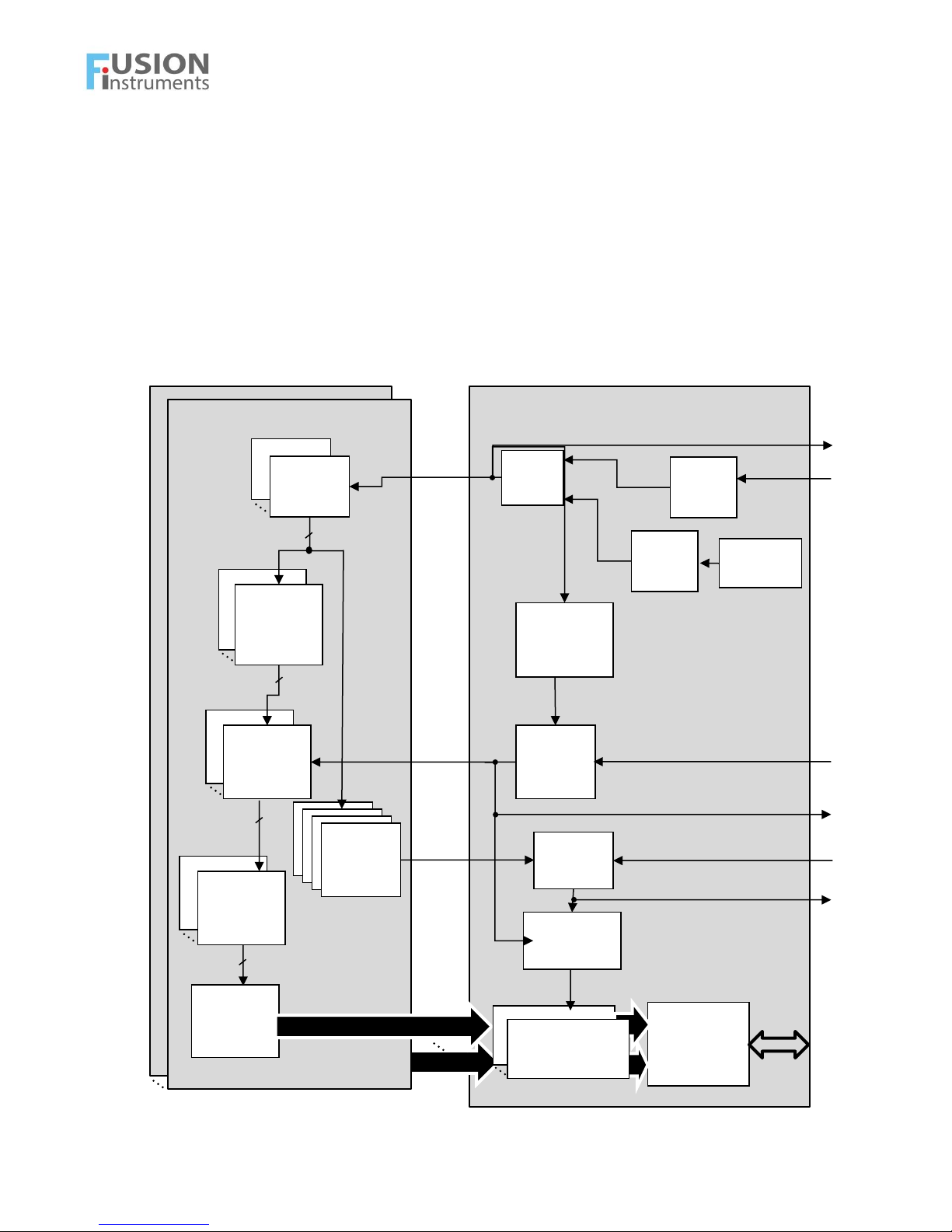
Figure 4. Block scheme of APDCAM-10G.
ADC
(32 channel)
Analog
Detector
1...4 detector, amplifier, ADC blocks
Timing
Timing
Data
Detector
5. APDCAM-10G Reference Manual
This section contains a detailed description of the APDCAM-10G system. Register tables are presented in Appendix F. The camera can be contolled by setting/reading values
to/from these registers using the low level Application Programming Interface (API) or
the APDTest program. A higher levels API provides more convenient functional programming interface, where details of the register maps need not be considered.
5.1. System Overview
The block scheme of APDCAM-10G is shown in Figure 4. The system has a modular design: it may contain 1-4 32 channel blocks. Each block contains an S8550 detector,
a 32 channel amplifier board with digital offset adjustment and a 32 channel Analog to
Digital Converter (ADC). The detectors are mounted in a detector panel onto a temperature stabilised cooling tab. At present a 4x32 channel and a 8x16 channel detector panel
is available in which 4 S8550 detectors are mounted either along their 4 or 8 pixel side.
The outer 2 detectors can be omitted in each setup resulting in 4x16 and 8x8 channel versions, utilizing 2 amplifier and ADC boards.
Calibration LEDs (max. 5) are mounted around the detectors. Their light level can be
controlled from the PC. Optical fibres can also be mounted around the detectors, which
lead light to the extension panel on the backside of the camera.
temperature
amplifiers
amplifiers
sensors
Power Unit
Ethernet
and timer
The photocurrent from each detector pixel is amplified by a sensitive low noise amplifier. Parameters of these can be specified at order time, they can be optimized for signalto-noise ratio at the expected light level. To compensate for the offset drift the output the
Page 15/62

APDCAM-10G User’s Guide
amplifiers they have a digital offset adjustment circuit. The analog signals are continuously digitized at 14 bit in the ADC boards. The timing of the ADCs is controlled by the
communication and timing unit, thus synchronized operation is guaranteed. Internal trigger signals can be generated inside the ADC boards thus measurement can be triggered
when signal crosses a channel-wise adjustable trigger level. The bit resolution of the optionally digitally filtered and resampled data stream can be reduced to 8 or 12 bits still on
the ADC boards. The resulting data stream is transmitted to the 10G communication
module via a high-speed internal serial connection. The maximum data transmission rate
from one ADC board is about 250 Mbytes/s corresponding to about 4 Msample/s measurement speed at 14 bit resolution per ADC channel. In case of two block systems this
can be doubled.
Data from all ADC blocks are collected by the 10Gbit communication unit and organized into UDP packets. The packets are transmitted to different software ports in the PC.
The Control and Power Unit provides power for all the other units and controls the detector infrastructure: detector bias voltage, temperature, calibration light, fans. The detector bias voltage can be set by the user up to a factory set limit in the range of 400-500
V. The exact limit is dependent on the individual detector and set in the factory. There is
also a minimum recommended detector bias voltage of 200 V, below that the crosstalk
through the pixels causes excessive noise.
Operation parameters of the camera are set by setting registers in the ADCs, the control and the communication unit and by sending commands to the communication unit.
All these communication tasks are performed by exchanging UDP packets between the
host PC and the camera. The last setting is stored in the camera, therefore after power
switch off/on the settings are preserved. There are a few examples from this rule, namely
the detector bias voltages are always disabled and the number of measurement samples
are set to 0 when the camera is switched on.
5.2. Detector and analog electronics
Each S8550 detector has 32 identical Avalanche Photodiode elements (pixels) connected to a common positive bias voltage. Up to 4 such 32 channel detectors can be installed in APDCAM-10G. Different layouts are shown in Appendix B while mapping
between pixels and ADC channels is shown in Appendix C.
The detector bias voltage determines the internal gain of the pixels. A typical gain
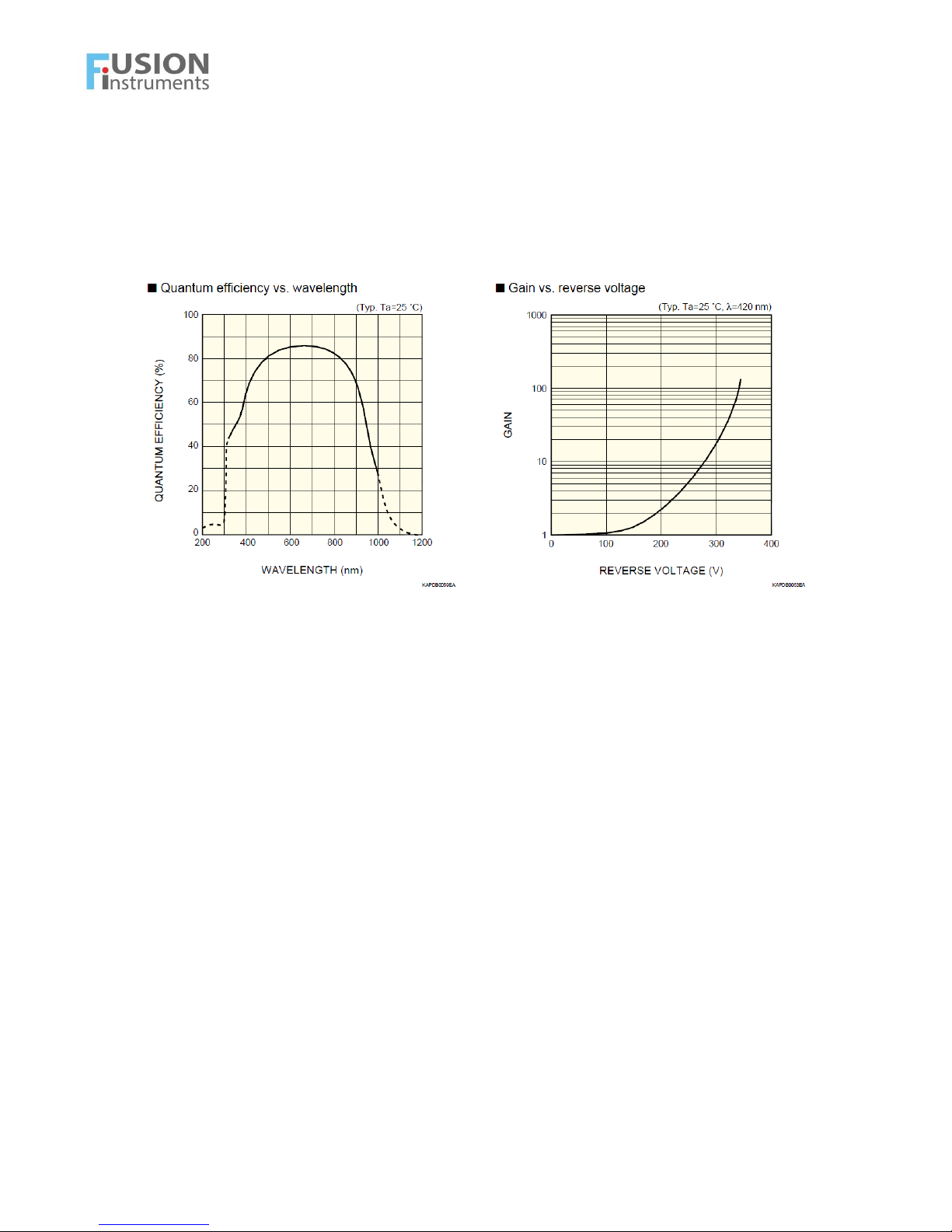
curve as a function of the applied voltage is shown together with the Quantum efficiency
(QE) in Figure 5. It has to be noted that different series of detectors may have considerably different gain curves but selected detectors with similar gain curves are installed in
one APDCAM. The voltage corresponding to the standard gain of 50 and the maximum
(breakdown) voltage is listed for each detector in the camera datasheet.
Besides the gain the bias voltage also changes the detector capacitance, it decreases
with increasing voltage. As pixels in one detector are operated from a common bias voltage at low voltage setting the crosstalk increases between channels. The result is an increase of the noise and its coherency between channels. Below about 200 V the 32 channel amplifier system oscillates between minimum and maximum output, therefore no
measurement can be done. The exact limit for oscillation and the noise as a function of
bias voltage depends on the amplifier bandwidth but above 200 V bias voltage the detector is stable. The noise level decreases slightly until about 350 V.
Page 16/62
APDCAM-10G User’s Guide
Figure 5. Detector typical Quantum Efficiency (QE)as a function of wavelength and Gain
as a funciton of bias voltage. (Source: Hamamatsu S8550 datasheet.)
The detector can be overloaded if high input light level is applied while the bias voltage is on. Although the detector and electronics is protected against overload, under the
most unfavourable conditions about 1W heat can be generated in the detector which
might result in damage if present for an extensive time. To prevent accidental overload
the bias voltage switch-on procedure consists of two steps: a general enable and a switchon command for each voltage generator. This procedure ensures that the bias voltage is
not switched on unintentionally. When APDCAM is switched on the bias voltage is off.
The detectors are mounted on a temperature controlled tab and detector temperatures
are measured at two places. The target detector temperature can be set in the control
module. This temperature can be either below or above the environmental temperature.
(The environmental temperature is measured on the base of the camera and can be read
by the user.) Cooling the detector usually does not provide advantage, but temperature
changes affect the detector gain, therefore the aim of temperature control is to provide a
stable gain.
The factory setting for the detector temperature is 25 degrees which is suitable for
most of the applications. The detector gain is increasing with decreasing temperature,
while the leakage current is decreasing. In very low light level applications, where the
leakage current statistical noise dominates lowering the temperature might improve the
signal to noise ratio. However, cooling for several hours significantly below the room
temperature might result in condensation and failure of pixels. These can typically be
cured by heating the detector to 40 degrees for a few hours, but no warranty is given for
condensation-related damages.
The analog electronics utilizes two amplifier stages for each channel, their bandwidth
is from DC to a maximum frequency. Parameters of the first stage (feedback resistor and
capacitance) determine the bandwidth and also the noise level. For setting an optimal
Signal to Noise ratio some information on the expected light level is required. As default
the amplifier is set up for about 1010 photons/s light level and 1 MHz bandwidth. For
considerable different conditions the amplifier should be mounted with different compo-
Page 17/62

APDCAM-10G User’s Guide
nents, therefore a rough estimation of the light level and required bandwidth is necessary
at manufacturing time.
The high sensitivity amplifiers and the detector bias current can cause some drift in the
signal DC level. In order to compensate for this the analog electronics is equipped with a
DC offset setting circuit which can be set for each channel individually in the data acquisition unit.
The detector and the analog electronics are mounted inside an Aluminium housing to
reduce noise pickup from the environment. However, from the front side the detectors are
open and the optical design should take care of sufficient electrical shielding.
5.3. Communication to the host PC
Communication to the host PC is done by the “10Gbit communication and timing
unit”. Internally this unit is connected to the ADCs and the control unit via an internal
bus. Each unit has a unique address. The control unit always has address 2 while the
ADC units are addressed at 8, 9, ... depending on the number of ADC units installed. The
ADC channels of the camera are numbered starting on the first ADC unit, that is 1...32 is
on the first ADC, 33...64 is on the second, etc. Although one APD detector contains also
32 pixels, pixels in one detector are not allocated to one ADC block. The correspondence
between APD pixels and ADC channels is listed in Appendix C.
The ADC and control units each have internal registers. At the lowest software interface level operational parameters of the camera can be defined and status can be determined by reading/writing to/from these registers. The registers can be reached by sending
UDP packets to the 10Gbit communication unit which then writes or reads the internal
registers. On a read operation the result is also sent back to the host in a UDP packet.
This process is implemented in the low level software interface as register read/write operation where the unit address and the register address constitutes the full address of the
operation. The high level software interface provides a functional access level to the
camera where individual register operations need not be taken care of the user.
Additionally to its registers the 10 Gbit communication and timing unit also has a
flash memory containing calibration and other information.
Communication to the 10Gbit communication unit is also done by sending UDP packets. Although this unit also has an internal register set it can be written only via functional
commands send in UDP packets. (Actually register read-write operations of the ADC and
control units are also done vie sending commands to the communication unit.) The status
of the unit can be still read by reading its registers. The list of commands, their parameters and details of the UDP packet structure are described in Appendices G-H.
Data from the ADC units are sent via a separate high speed serial communication lines
to the 10G unit. The maximum speed of this connection is about 2 Gbits/s which results
in an acquisition speed of somewhat over 4 Msample/sec if all 32 channels are operating
in an ADC unit with 14 bit resolution. If only two ADC units are installed in the camera
two data lines are used per ADC unit, therefore the speed is doubled.
Data from one ADC unit are collected into UPD packets. In order to ease data collection data from different ADC units are sent to separate software ports on the PC. As the
data transmission rate is high it is essential to set up the receiving PC networking paramters in a proper way, as described in Section 4.4. APDCAM normally uses jumbo size (8
kByte) UDP packets are used otherwise the PC may be overloaded at high speeds. Some
Page 18/62
APDCAM-10G User’s Guide
32 channel ADC unit
Clock in
ADC
PLL
Sample
ADC
(32 ch.)
ADC
Trigger in
Sample in
Digital
(32 ch.)
ADC
Data out
ADC Data
(32 ch.)
Trig.
compare
Ring
(32 ch.)
Figure 6. Block scheme of data acquisition.
32x8,12 or 14 bit
32x14 bit
32x8,12
Channel
combiner
Trigger out
Sample out
Clock
select
Ext.
Sample
select
32 channel ADC unit
Sample
10 Gbit
To
host
Trigger
Data
Clock out
Enable
Trigger
Sample
UDP packet
generator
32x8,12
10Gbit communication and timing unit
Internal
20 MHz
network components don’t allow jumbo packets therefore it is advisable to connect the
camera directly to the host. The 10Gbit link also imposes a speed limit for data acquisition as typically 8 Gbit/s effective bandwidth is available. This matches the internal limit
of 2 or 4 Gbit/s per ADC unit, depending on 2 or 4 ADC units therefore the 10Gbit link
does not pose an effective speed limit. Details of data communication are described in the
software documentation.
5.4. Data Acquisition
. The block scheme is shown in Figure 6. Data acquisition is performed by the 10Gbit
communication and timing unit and 1 to 4 ADC blocks each digitizing 32 analog signals.
The digital data from one 32 channel ADC block is packed into a data scream and sent on
Resample
or 14 bit
buffer
Filter
level
Clock
Clock
PLL
Clock
Clock
Divider
(SAMPLEDIVIDER)
source
select
or 14 bit
counter
(SAMPLECOUNT)
PC
Ethernet
interface
Page 19/62
 Loading...