

Page 1

MARINE RADAR
MODEL
MODEL 1622
Page 2

C
9-52, Ashihara-cho,
Nishinomiya, Japan
Telephone: 0798-65-2111
Telefax: 0798-65-4200
All rights reserved.
Printed in Japan
Your Loc al Agent/Dealer
FIRST EDITION: FEB. 2000
B: SEP. 12, 2000
(KAOK)
PUB. No. SME-34520-B
MODEL 1622
Page 3

CONTENTS
Chapter 1. General
1.1 Display Unit.................................................................. 1
1.2 Scanner Unit.................................................................. 2
Chapter 2. Block Description
2.1 General.......................................................................... 3
2.2 Display Unit.................................................................. 4
2.3 Scanner Unit.................................................................. 5
2.4 Functions of Each Circuit board ................................... 6
Chapter 3. Adjustment
3.1 Display Unit.................................................................. 13
3.2 Scanner Unit.................................................................. 14
Chapter 4. Maintenance
4.1 Maintenance Parts......................................................... 15
4.2 Replacement of Major Parts.......................................... 16
4.3 How to change system program.................................... 21
Chapter 5. Troubleshooting
5.1 Maintenance Menu........................................................ 22
5.2 Error Messages.............................................................. 23
5.3 Troubleshooting Matrix table........................................ 23
5.4 Test points on Each Board ............................................ 25
Exploded View
Schematic Diagram
Electrical Parts List
................................................................. D-1
....................................................... S-1
....................................................... E-1
Page 4
Chapter 1. General
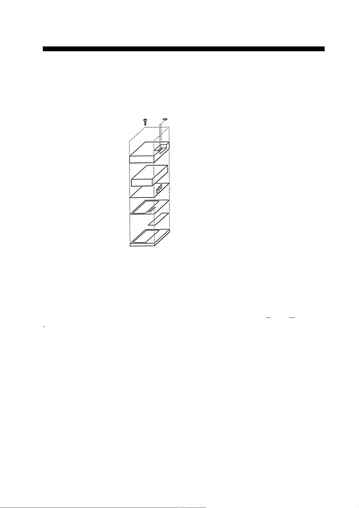
1.1 Display Unit
All parts are sandwiched together and fastened by four screws and three connector fixing nuts
from the rear side.
Resin cover
Shield cover
DU Board
LCD Display
PNL pcb
Panel cover
Figure 1-1. Construction of Display Unit
Protection against EMI
Many radars use conductive paint inside their covers to protect against EMI (Electro Magnetic
Interference). This model, however, is not painted, but has a shield cover over the DU board for
protection against EMI.
Waterproofs
The display unit conforms to the IEC standard IPX5; namely, waterproof against water jets. Even
the small hole to the right of the arrow keys, which is where the aural alarm is released, is
waterproof. A “breathing sheet” between the panel cover and the buzzer all ows ai r to pass and
prevents water from being drawn into the enclosure during atmospheric pressure changes.
1
Page 5

1.2 Scanner Unit
1.2 Scanner Unit
The scanner unit mainly consists of INT Board (03P9271), IF AMP Board (03P9269), MIC (RU-
9458), radiator, antenna motor, reed switch which generates HD signal, magnetron, and MD
Board
(03P9270).
Power to Scanner Unit
The ship’s mains is directly supplied to the scanner unit, where various voltages are made.
Therefore, if the antenna cab le length o f 12VDC set is 20m or more, scanner rotation may
be abnormal due to voltage drop. If the antenna cable is more than 20m, modify the unit
to 24VDC set.
Antenna Cable
Both the scanner unit and the display unit have a CPU. T he y communicat e with each other on
two lines, “COM (HOT)” and “COM (COLD)”. The result: the number of lines in the cable was
reduced.
1 GAIN
2 STC
3 TUNE
4 TUN.IND
5 MOTOR(+)
6 MOTOR(
7BP
8HD
9 P/L-A
10 P/L-B
11 TRIGGER
12 VIDEO
13 GND
14 +12V
15 -12V
16 GND
17 SHIELD
Conventional radars MODEL 1622
-
)
COM (HOT) 1
COM (COLD) 2
BP/HD 3
TRIGGER 4
VIDEO 5
GND 6
S.M. (HOT) 7
S.M. (COLD) 8
GND 9
SHIELD 10
Figure 1-2 Antenna Cable
2
Page 6
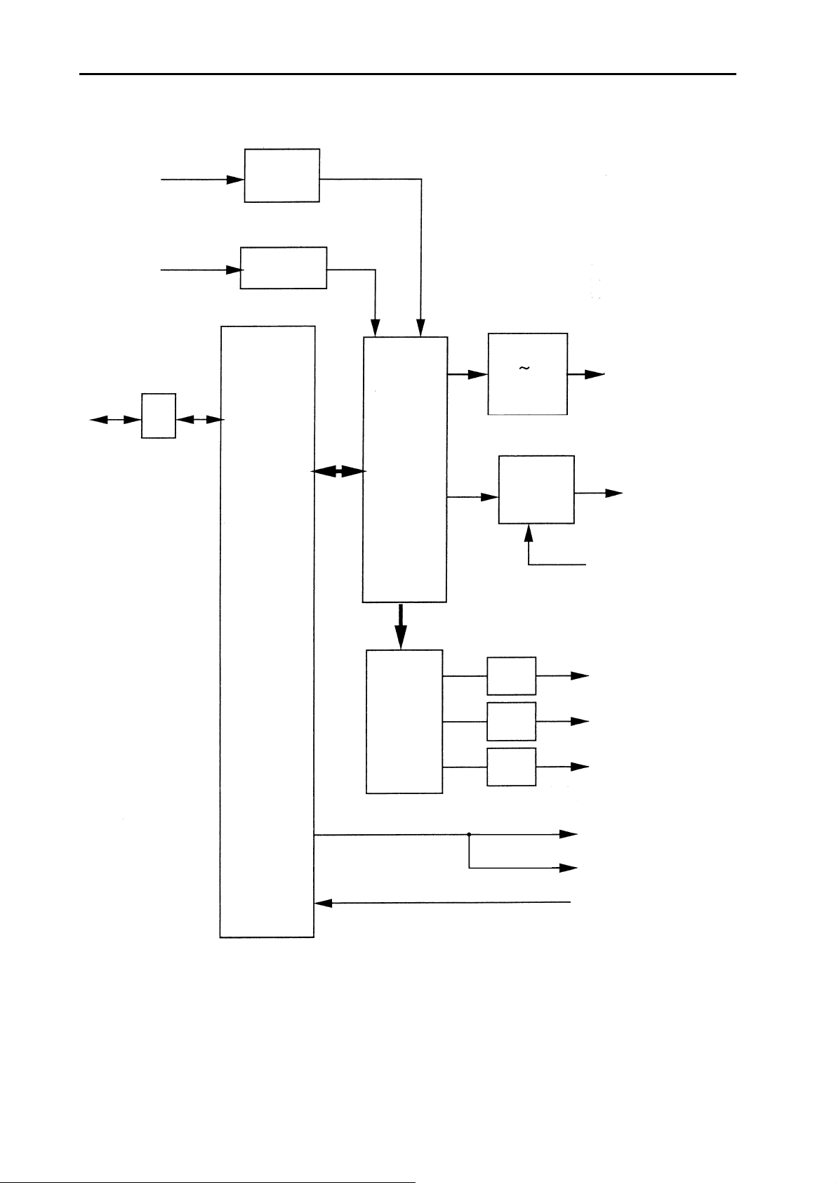
Chapter 2. Block Description
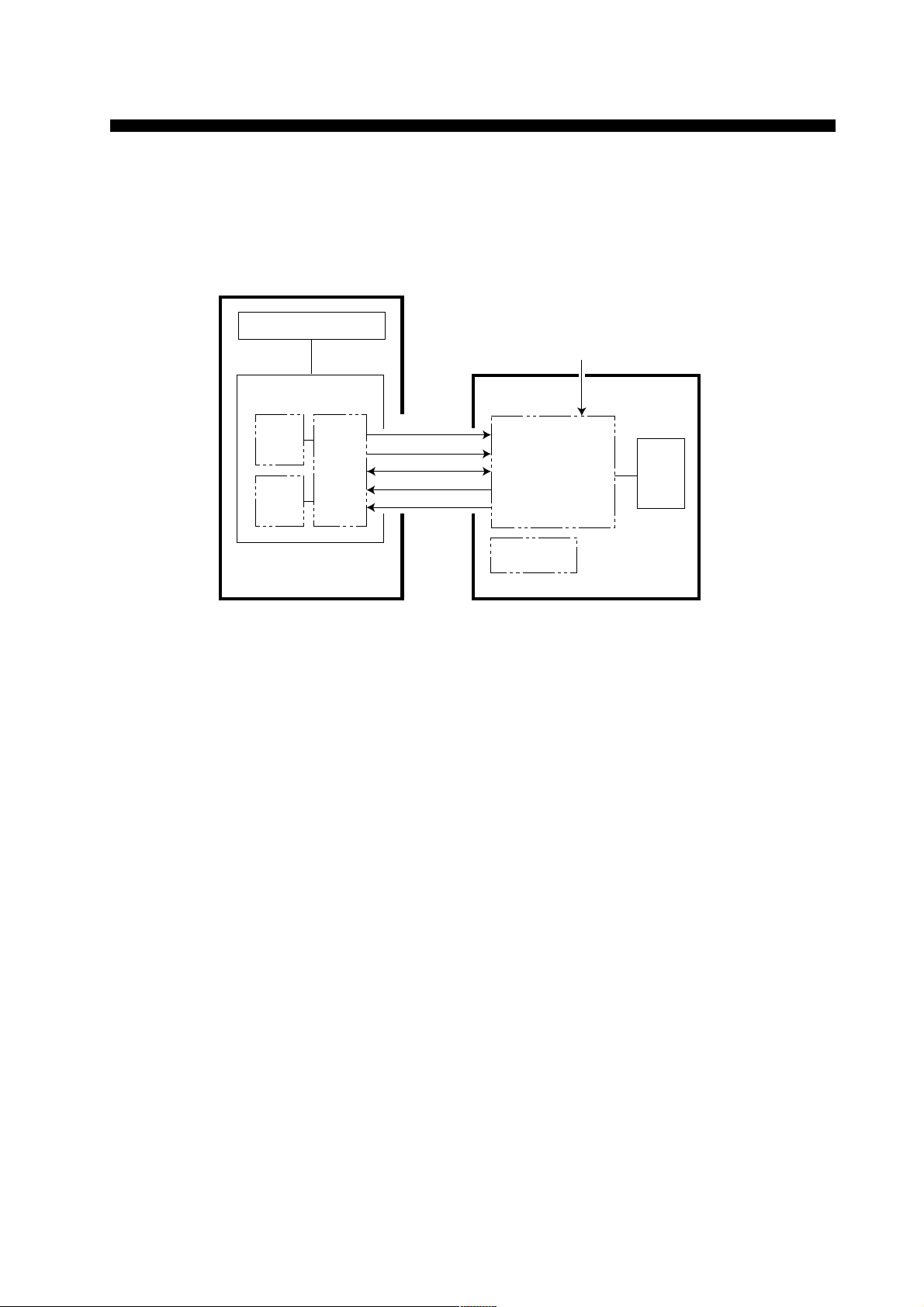
2.1 General
The CPU on the DU board of the display unit communicates with the CPU on the SD board of
the scanner unit in RS-422 format.
Radiator
Ship’s mains
Transceiver
MD
Board
Board
IF
Board
INT
Video signal
BP/HD
Communication (H.C)
Trigger
Ship’s mains (H.C)
Display Unit
DU Board
Signal processor
& power supply
PNL Board
LCD
Scanner Unit
Figure 2-1. Simplified Block Diagram
The trigger pulse from the DU board is modulated at the MD board to oscillate the magnetron.
The echo received by the antenna is amplified by the IF amplifier and is fed to the DU board as a
video signal. The DU board converts the analog signal to digital signal and processes to display
it on the LCD.
Bearing pulse (BP) and heading signal (HD) are generated in the scanner unit and received by
the DU Board in the display unit.
3
Page 7
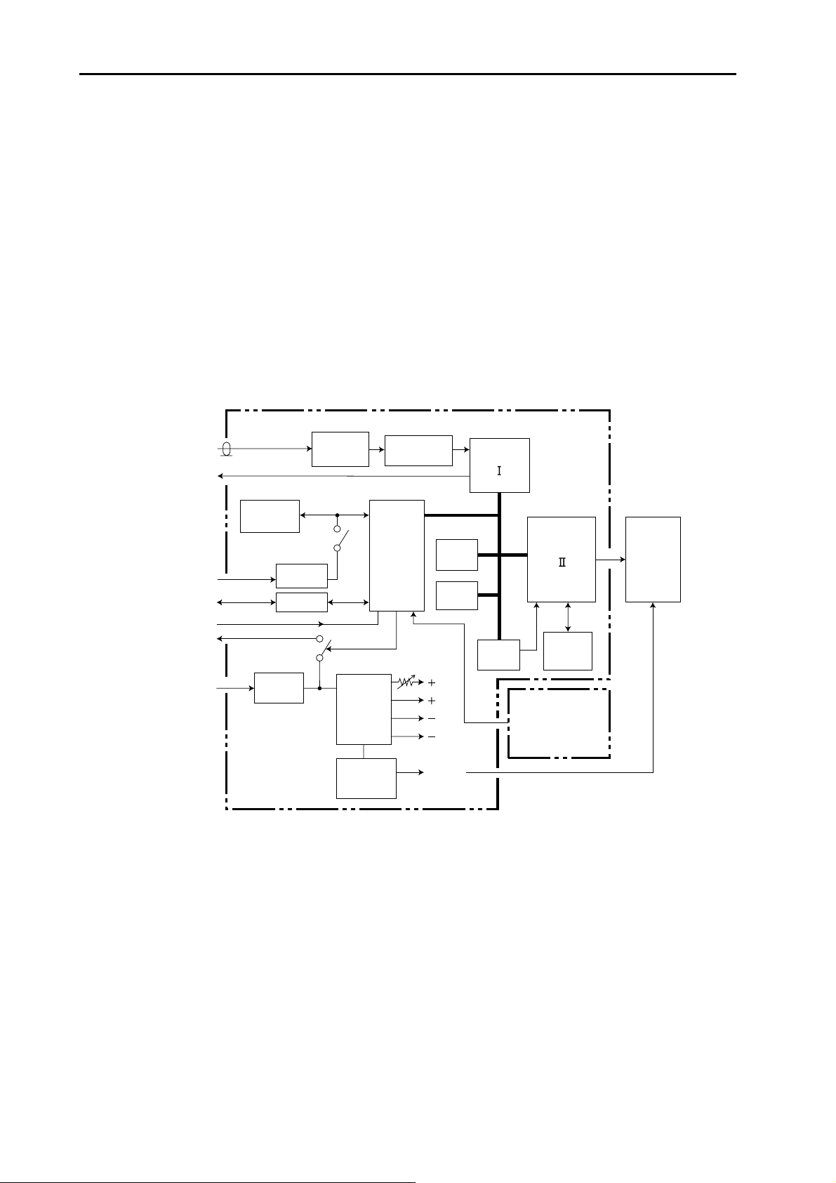
2.2!Display Unit
2.2 Display Unit
The display unit features that;
1) DU Board produces LCD back-light voltage of 210VAC.
2) An artificial echo signal (instead of the video signal) can be selected.
3) The interface comm unicates wit h t he scanner unit in RS - 422 format.
The TX trigger is made at the gate array (!) and is fed to the scanner unit. The received video
signal is A/D converted and is sampled at the gate array (!). The echo on each sweep is stored
on the V-RAM via the gate array ("). Upon receiving the heading pulse, the stored data are
output to the LCD in four shades of gray, according to echo strength.
From Scanner
To Scanner
From NAV AID
To Scanner
From Scanner
To Scanner
Ship’s Mains
VIDEO
TRIGGER
EEPROM
U105
NMEA
RS-422
BP-HD
FILTER
L1,L2
DU Board
03P9268
I/F
I/F
U107,C104
U114
U126
U119
FTC
R112
DC-DC
CONV.
U6,Q6,T1
R-C
CONV.
Q52,Q53,T2
A/D CONV.
U101
CPU
U108
ADJ
Back-Light volt.
AC210V
ROM
U115
RAM
U109
5V
12V
6V
22V
GATE
ARRAY
(
)
U111
GDC
U112
GATE
ARRAY
(
)
U108
V-RAM
U113
U116
PANEL Board
PNL9194
LCD
03S9461
Figure 2-2. Block Diagram of Display Unit
4
Page 8
2.3!Scanner Unit
2.3 Scanner Unit
The scanner unit features that ;
1) The powers supply circuit for the scanner unit is provided on the SD board.
2) The SD board in the scanner unit communicates with the display unit.
3) Auto-gain and auto-STC circuits make operation easy.
The TX trigger from the display unit is modulated and oscillates the magnetron. The received
echo is fed to the MIC and is amplified at the IF amp. The output is divided two lines: one is led
to the display unit and the other is applied to the interface for auto-gain and auto-STC functions.
Display
Unit
INT Board 03P9271
INTERFACE
Auto Gain
Auto STC
Auto Tune
Communication
COM
Motor Drive
BP/MD
TRIGGER
SHIP’S
MAINS
POWER
SUPPLY
Figure 2-3. Block Diagram of Scanner Unit
IF Board 03P9269
VIDEO
GAIN
A/C SEA
TUNE
12V
5V
8V
TX-HV
MD Board 03P9270
IF AMP
MODULATOR
TUNE
IF
Magnetron
MIC
RU-9458
(U801)
Circulator
E3588
(V801)
ANT.
03P9267
M
RM-9455
(B801)
5
Page 9

2.4!Functions of Each Cir c uit board
2.4 Functions of Each Circuit board
2.4.1 Display Unit
The display unit consists of DU board (03P9268), PANEL board (PNL9194), and LCD indicator
(03S9461).
PANEL Board
Mounted on this board are the operating keys, panel-illuminating LEDs, and electrical buzzer,
constituting the man-machine interface.
DU Board (03P9268)
The reference oscillator U125 is a quartz oscillator which generates an accurate and stable
reference frequency signal. This reference frequency signal is the source of the transmission
trigger, the clock for video signal processing in the display unit, the time-base signal, the
reference clock for LCD display, the reference clock for CPU, and so on.
According to the distance range selected in the panel operation, CPU computes the ratio of
dividing the reference frequency and sends the data to the gate array U111 (radar signal
processing circuit). Based on the data, U111 creates the transmission trigger from the reference
frequency signal.
This radar intentionally varies the pulse repetition frequency of the transmission trigger to
prevent the interference signals fr o m other radars.
The IF video signal from scanner unit inputs to the vi deo circuit on the DU board.
The video circuit includes FTC circuit that rejects the reflecting signals from the rain and snow.
CPU switches on or off the FTC function according to the panel operation.
The IF video signal is converted by a A/D converter to the three-level digital signal, which inputs
to the gate array U111 (radar signal processing circuit). In U111, the input digital IF video signal
is sampled with the sampling clock corresponding to the range setting. Further in U111, when
the interference rejector is turned on in the menu, each receiving video signal is correlated with
the corresponding transmission to reject the interference signals from other radars. The video
signal output from U111 is written in the VRAM U116 for the display.
The antenna bearing signal and heading signal are input to CPU from scanner unit. The heading
correction data, obtained at heading alignment (instllation menu) is stored in EEPROM U105,
and CPU computes the correct direction of the antenna, using the correction data. The data to
correct the difference between the transmitting and receiving timing is obtained at TX time delay
adjustment (installation menu) and is also stored in EEPROM U105. The correction is carried
out in U118.
6
Page 10

2.4!Functions of Each Cir c uit board
While the target scanning system of the radar uses the method of R#$ coordinates, LCD
display of this radar employs the method of X-Y coordinates, which is similar to so called TVsweep method.
The sweep time of the LCD display is independent of that of the radar scanning system, so
VRAM U116 is provided as the interface between them.
In order to write the radar echo signal received after every transmission trigger on VRAM U116,
CPU converts the antenna bearing signal $ into the values of SIN$ and COS$ and send
them to U118. U118 further converts them to X-Y coordinates of RSIN$ and
RCOS$. These values are used as the address to write the radar video signal on VRAM U116.
VRAM U116 also holds the past video signal for display f or a trail time specified by the panel
operation.
According to the settings of the operating panel, CPU writes on VRAM U113 the display data
such as the fixed range rings, EBL, VRM, cursor, guar d alarm range, and scale of azi mu th angle.
Further, CPU also writes on VRAM U113 the character and numbers to be displayed on the
screen. For writing these data, GDC U112 is used.
The data writing/reading onto/from the VRAM is carried out by U118 in time- sharing method.
The display data are read out from VRAM and sent to LCD display using GDC U112.
The signals for controlling scanner unit (including the transceiver) are converted to RS-422 serial
signals in U119 and sent through a balanced RS-422 cable so that the signals may not be affected
by external noise. The control signals include those for switching the transmission on/off,
adjusting the transmitting pulse width and IF amplifier gain, and adjusting STC.
The information from the navigational aid is received through U114 and U126 to be displayed on
the radar screen.
The unit requires power supply source ranging 10.2 to 31.2 V DC. This voltage meets the
voltage requirement for ships: 10% lower and 30% higher than 12V/24V ship’s mains. This DC
power is supplied through noise filters, L1, and L2, to the pulse-width-controlled DC-DC
converter mainly consisting of U6, Q6, and T1, which generates the stable voltages of +5 V, +12
V, -6V, and -22 V that are needed in display unit. The voltage +5 V is mainly used for the digital
circuits, +12 V and -6 V are used for the video and other analog circuits, and –22 V is for the
LCD display. The DC-AC inverter consisting of Q52, Q53, and T2 generates AC 210 V which is
used for the backlighting of the LCD display.
If the power supply is reverse-connected to the radar, the reverse-polarity protector activates so
that the circuit breaker is tripped or fuse is blown off to prevent the damage to the unit.
The power supply circuit contains low- and high-input voltage protectors.
7
Page 11

2.4!Functions of Each Cir c uit board
2.4.2 Scanner Unit
INT Board (03P9271)
INT board contains: one-chip CPU U3, that includes the RAM, ROM, and analog ports; U5
including I/O ports the stepping motor drive circuits; and U7 including the A/D converter which
outputs tuning, gain, and STC control signals.
The output from U7 is used to control the STC and gain of the IF amplifier and the frequency of
microwave local oscillator for MIC.
The operating conditions of the radar that have been set on the operating panel of the display unit
are sent to the CPU U3 on the INT board through the RS422 communication line. The CPU U3
controls the stepping motor drive circuit U5 which drives the stepping motor to rotate the
antenna. The antenna azimuth signal is created in the stepping motor drive circuit and mixed
with the heading signal (S801), and sent to the display unit.
In order to change the transmitting radar pulse length according to the selected range, the pulse
width information is sent from the INT board to the modulation circuit on the MD board.
There are the automatic mode and manual mode to adjust the gain of the IF amplifier. In the
automatic mode, CPU U3 monitors the video signal from the IF amplifier, and the monitored
signal inputs to the A/D converter U7 through the I/O port U5, and the A/D converter output
controls the IF amplifier gain. In the manual mode, the signal set by manual setting inputs to the
A/D converter, and the A/D converter output controls the gain of the IF amplifier.
This radar employs an automatic tuning system in which the main bang signal from the IF
amplifier is amplified and inputs to CPU U3 as the signal indicating the tuning level.
The CPU U3 controls the output of the A/D converter U7 so that the tuning indication level may
become maximum.
The adjustment of STC is also carried out in the same way as the gain adjustment.
IF Amplifier Board (03P9269)
The IF amplifier, the intermediate frequency of 60 MHz and band width of 7 MHz, consists of
Q1, U1, U2, and a buffer Q4. This board includes the gain and STC control circuits consisting of
Q2 and Q3. Another circuit, consisting of Q5 to Q10, detects the main bangs to indicate the
tuning level.
8
Page 12

2.4!Functions of Each Cir c uit board
RU-9458 Module
This module includes the circulator and MIC circuit that converts the microwave frequency to
the intermediate frequency.
The circulator switches between the transmitting and receiving microwave circuits so that the
transmitting radio energy may be efficiently transmitted to the antenna without leaking to the
receiver side and the receiving radar signal fr o m the antenna may be sent with efficiency t o the
receiver without leaking to the transmitter side.
The receiver side is provided with the waveguide to coaxial converter, diode limiter, and
balanced mixer. The diode limiter, set after the converter, protects the balanced mixer from the
excessive input power, and the mixer converts the input microwave signal to the 60-MHz IF
signal.
A voltage-controlled FET oscillator outputs the signal to the mixer.
MD Board (03P9270)
The power supply circuit and modulation circuit of the scanner unit (transceiver) are mounted on
the MD board.
There are provided two DC-DC converter power supply circuits: one supplies –6 V, +5 V, and
+12 V to the circuits except the magnetron and the other supplies power to the magnetron heater
and TXHV. The two DC-DC converters generate stable voltage outputs with Q803 and Q832
driven by the pulsewidth controllers U801 and U805.
The magnetron current, -6 V, +5 V, +12 V, +8 V (magnetron heater voltage), and TX HV can be
checked at the check points TP804 on the board.
In the magnetron modulation circuit, the transmitting pulse waveform is determined by the oneshot multivibrator U851 which is triggered by the transmitting trigger pulse. The pulsewidth of
the multivibrator is set by the time constant which is determined by the pulsewidth control signal
from INT board. The output of the multivibrator inputs to the FET switching transistor Q857
through transistor buffer Q853 and variable resistor VR851. The VR851 presets the voltage for
driving Q857 to determine the magnetron output power.
9
Page 13
2.4!Functions of Each Cir c uit board
VIDEO
RS422
TRIG
U1
U4
Amplifier
Q1
Buffer
U5
I/O PORT
BP
Q6
Q3
Buffer
Q11 Q12
Q13
Mixer
Antenna
motor drive signal
BP/HD
HD Marker
U3
CPU
U7
D/A
Buffer
Q14
Q15
Q16
PL B
PL A
TUNE IND
Figure 2-4. Block Diagram of INT Board (03P9271)
GAIN
Control
STC
Control
Tune
Control
10
Page 14

TX HV
8V
2.4!Functions of Each Cir c uit board
MAG.CUR.
TUNE GATE
6V
CR831
12V
CR832
5V
U804
Regulator
VR801
T802
CR837
CR838
Q832
CR836
U805
Inverter driver
L851
TP804
MAG.CUR. HV.CHECK5V 8V
12V
CR855
T851
Medulation
Q857
transformer
Q855
VR851
Q853
Q856
Buffer
Buffer
Q801
6V
Q801
Pulse width
Q803
Ship’s mains
controller
Q801 Q802
Q805 CR804
Error detector
Q851,Q852
PL-A
Figure 2-5. Block Diagram of MD Board (03P9270)
11
Pulse width
decoder
PL-B
U851
Pulse width controller
TRIG
Page 15

2.4!Functions of Each Cir c uit board
STC Control
GAIN Control
Trigger
VIDEO
Output
TUNE GATE input
TUNE IND output
Q2 Q3
GAIN
STC
Controllers
Q4
Buffer
U2 3rd
IF AMP
Video detector
60MHz IF
LC filter
U1
2nd
IF AMP
Q5 to Q10
Tune level
detector
60MHz IF
LC filter
Figure 2-6. Block Diagram of IF AMP Board (03P9269)
Q1
Q1
1st
1st
IF AMP
IF AMP
60MHz
IF-IN
12
Page 16

Chapter 3. Adjustment
(
)
DANGER
Both display and scanner units use high voltage electricity, which
endanger human life. Precautions must always be exercised when
reaching inside the unit. (1 kVAC for LCD backlighting and 300
VDC for TX)
3.1 Display Unit
Voltage check
Remove the resin cover, and measure each voltage. It is not necessary to open the shield cover
on the DU board.
Table 3-1
Item Setting Test point Ratings Adjuster
"
"
&
&
5 V
12 V
22 V
6 V
TX
#
8NM
ST-BY
ST-BY
ST-BY
$
#"$%
TP4
J1#7
J1#10
J1#9
#"$%
#"$%
#"$%
#&$
TP5
#&$
J1#5
#&$ &
J1#5
#&$ &
J1#5
4.95'5.05 Vdc
11.2'12.4 Vdc
'&
22.9
6.0
'&
20.7 Vdc
5.0 Vdc
VR2
J1
TP4
"
5V
VR2
Figure 3-1. Test points on DU Board
13
Page 17

3.2 Scanner Unit
Voltage check
Open the radome, and measure each voltage with the modulator cover removed.
Table 3-2
Item Setting Check point Rating Adjuster
"
12 V
"
8 V
heater volt.
TX-HV
(divided)
Magnetron
current
ST-BY
ST-BY
TX(Note)
(3NM)
TX(Note)
(3NM)
TP804#3
TP804#4
TP804#6
TP804#4
TP804#7
TP804#4
TP804#5
TP804#4
#"$%
#&$
#"$%
#&$
#"$%
#&$
#"$%
#&$
11.9'12.1 Vdc
7.8'8.2 Vdc
8.5'9.35 V
2.8'3.6 V
3.2!Scanner Unit
VR801
VR851
Note) To transmit with scanner rotation suspended, turn on the power while pressing and
holding down the%&'key. After one minute, the radar is in transmission mode.
VR851
VR801
TP804
Figure 3-2. Test points on MD Board
14
Page 18

Chapter 4. Maintenance
This unit is designed for board level maintenance, not component replacement.
4.1 Maintenace Parts
Table 4-1 Maintenance Parts
Parts Type Code No. Remarks
DU Board 03P9268 008-499-680
PNL Board PNL9194 008-481-680
MD Board 03P9270 008-499-650
IF Board 03P9269 008-499-640
INT Board 03P9271 008-499-660
LCD Unit DG52Y-5MC 000-142-310
MIC S-RX50/RU-9458 000-142-269
Magnetron E3588 000-142-270
Antenna Motor RM-9455 000-142-252
Fuse FGBO-A, 5A, 125 V 000-549-064
Program ROM PROM0359158101 008-499-730 U115, DU Board
Radome cover RSB- 0060 008-440-720
Radome packing 03-118-3203 100-185-430
15
Page 19

4.2!Replacement of Major Part s
4.2 Replacement of Major Parts
Removing display unit cover and shield plate
1. Loosen and remove the nuts from three jacks at the display unit cover.
2. Remove four screws fixing the display unit cover.
3. Remove the display unit cover, the shield cover will be exposed.
4. Of the two shield tapes attached to the shield cover, remove the shorter one.
5. Remove four screws fixing the shield case.
6. Lift up the shield case to expose the board.
Shield tape
Figure 4-1. Display Unit, rear view
Figure 4-2. Display Unit, cover removed
Reassembling
7. Fix the shield case to the board with four screws.
8. Attach the shield tape (shorter one) supplied to the same position as before.
!!!!""""
Shield case
Space
P.C. Bo ar d
Chassis
Figure 4-3. How to run shield tape
9. If the longer shield tape came off during work, exchange it with new one.
Parts Name Type Code No.
Shield tape DK-102-35/ L=45
Shield tape DK-102-19/ L=110
#$%&'()*+,&
P.C. Bo ar d
Chassis
10. Make sure that each of three jacks on the board is fitted with a gasket.
11. Put the display unit cover back in position.
12. Set and tighten three nuts and four screws to fix the jacks and the display unit cover.
16
Page 20

Panel(E) 03-135-1021
4.2!Replacement of Major Part s
Cover
LCD Assy.
Round side
O-ring (large)
LCD
DG 052Y-5MC
A
(P)DU
03P9268
View from A
LCD
Never run wires beyond this line.
Figure 4-4.
O-ring (small)
J3
VH connector wires from LCD
Shield plate
03-146-1002
P2, 4P VH connector
Figure 4-5.
17
J2
PCB fixing plate, 03-118-1001
P3, Flat cable
Page 21

Panel packing
03-118-1006
4.2!Replacement of Major Part s
(P)PNL
PNL9194
PW sheet
86-009-1022
Rubber key(E) 03-135-1022
Figure 4-6.
18
Page 22

STS Belt and Motor
1. Unscrew four M3(8 screws (() fixing the bearing retainer.
2. Remove the radiator assembly.
3. Replace the belt (or motor) with new one.
No tension adjustment of the belt is necessary.
4. Assemble the unit by reversing above steps.
M3
6 SCM3
Driving Pulley
03-146-3304
4.2!Replacement of Major Part s
Radiator Assy.
Fix at the
same time.
M3
B801 Motor
RM-9455
STS Bert
40S2M266UG
8 2pcs.
Connector
M3 8 4pcs.
Driver Pulley
tw
o
d
o
w
e
ls
dowels
B
Bearing
Retainer
Use this hole to loosen
the screw fixing the
bearing retainer.
Driver pulley, top view
STS Belt
Driving pulley
View from B
Driver pulley
Figure 4-7.
19
Page 23

4.2!Replacement of Major Part s
Magnetron
Handle the magnetron, taking the followings into account.
1. Use a non-magnetic screw driver to dismount and mount the magnetron.
2. Keep the magnetron 25mm away from the metals.
3. Never pull the magnetron lead wires.
MIC
See figure below.
M4 20
Remove shorting plug.
Dowels
Dowels
IF
03P9269
J810
Figure 4-8.
J808
U801
S-RX50
M4
10 4pcs.
V801 Magnetron
E3588
20
Page 24

4.3!How to change system progr am
4.3 How to change system program
PROM, U115 on the DU Board stores system program. Change the ROM to update the program.
Raw ROM Type : M27C1001-10F1
Program No.: 035915800X
Replacing pr ogr am ROM
1. See page 18 to gain access to the DU board.
2. Remove the lock band of the program ROM (U115)
3. Detach the program ROM from the socket by using a dedicated tool or a screwdriver.
4. Insert the update ROM (0359158104) to the socket.
U115(PROM)
5. Secure the ROM by using the lock band previously removed.
Figure 4-9. DU Board (03P9268)
How to read program number
1. Turn the radar on.
2. Wait until the initial screen appears, then press and hold UP and DOWN keys together.
3. In about 10 seconds, the maintenance menu as shown below will appear.
4. Press MENU key to close the menu.
21
Page 25

Chapter 5. Troubleshooting
The unit does not provides self-test functi on. Th is chapter mainly describes how t o check each
block.
5.1 Maintenance Menu
To open the maintenance menu;
1. Turn the radar on.
2. Wait until the initial screen appears, then press and hold UP and DOWN keys together.
3. In about 10 seconds, the maintenance menu as shown below will appear.
4. Press MENU key to close the menu.
Figure 5-1. Maintenance Menu
1) Reading program Number:
The program number appears at the upper left corner.
2) When connecting M1621MK2 scanner unit
The scanner unit of M1621 and M1621MK2 can be connected to the display unit of M1622.
For this combination, the MODEL in the maintenance menu must be set to “1621/M2” which
provides magnetron warm-up time of 90 seconds. The use in wrong setting may shorten the
life of the magnetron or damage the magnetron. The scanner unit of the M1622 is designed
for the warm-up time of 60 seconds.
3) Selecting “Demo display”
Select “Demo” to display the preprogramm ed echo on the screen.
4) Receiving signal (Nav data)
The sentence of nav data receiving from the navaid is shown by reversed video.
22
Page 26

5.2!Error massages
5.2 Error Messages
The following messages appear to call the operator’s attention to missing heading or bearing
pulses. Check the scanner cable for damage or disconnection when these messages appear.
Table 5-1. Error Messages
Message Meaning
HD-SIG-MISS
BP-SIG-MISS
Heading pulse is not applied to the CP U on the DU board.
The heading mark disappears .
Bearing pulse is not applied to the CPU on the DU board.
Radar automatically changes from TX to ST-BY mode.
5.3 Troublesh ooting Matrix tabl e
The troubleshooting matrix table on the next page helps the service technician to quickly identify
defective pcb or block. To use the table, locate the symptom in one of the three columns of the
table. Possibly defective circuits and their likelihood of defectiveness, indicated by a circle, star
or triangle, corresponding to 70 to 80%, approximately 20% and a few percent respectively, are
listed in each column. Numeral inside circle shows degree of possibility; the smaller the number,
the higher the possibility.
Note) Before consulting the table, check the ship’s mains (input voltage at J1351#1(+) and
#2(-) of the display unit: 10.2 to 31.2VDC) and the power fuse.
23
Page 27

5.3! Troubleshooting m atrix table
7) Incorrect target bearing.
9
8
7
8) Poor sensitivity.
9) Keyboard is pressed but no response.
6
5
)
+
)
+
*
*
*
)
+
*
)
)
,
,
4) Marks and legends do not appear.
1) Power can not be supplied.
Symptom
nor echo.
5) Marks and legends appear, but no noise
echo.
6) Marks, legends and noise appear but no
2) Power is supplied but nothing
3) Scanner does not rotate.
appears on LCD.
4
3
2
1
)
,
)
,
+
)
*
)
!!!!!!!!
Check Point
!!
DU PCB 03P9268
PNL PCB 03P9194
$
5A
#
LCD Display, DG52Y-5MC
IF PCB 03P9269
MD PCB 03P9270
INT PCB 03P9271
Magnetron
MIC
Motor and belt
Fuse
24
Page 28

5.4!Test points on Each Board
5.4 Test points on Each Board
1) DU Board)03P9268*
Test point Check Item Ratings Remarks
TP1
TP2/TP1
TP3/TP1 Q6-D
TP4/TP1
TP5 GND GND
TP7/C55 INV
TP11/TP5 XTAL
TP12/TP5 BLCK
TP13/TP5 TRIG
TP14/TP5 BP
TP15/TP5 HD
TP16/TP5 VIDE
&
DC
"
9V 8.7'9.9Vdc
21.7'29.4us
"
5V 4.8'5.2Vdc
11.2'14.5V-68'92kHz
36.85'40.85kHz
8.1725'10.7125kHz
V=9.0'12.0
T=6.0'10.0us
V=4.0'5.2V
T=5.5'6.5ms
V=4.0'5.2V
T=2.5'2.9S
Same wave as
TP602, IF Board (03P9269)
.
U3-#5
Switching Waveform (Primary)
Adjuster: VR2
Same reading at between J1#2(+) and J1-#5(- )
DC-AC Inverter, Primary
BLCK, U118-#87
TX Trigger, U1 11-#60
Bearing, U118-#138
Heading, U118-#137
Video, DJ1-#6
2) MD Board)03P9270*
Test point Check It em Ratings Remarks
TP801/TP802
TP803/TP802
TP804-1/ TP804-4
TP804-2/ TP804-4
TP804-3/ TP804-4
TP804-5/ TP804-4
TP804-6/ TP804-4
TP804-7/ TP804-4
TP805/TP806
TP807
TP808
TP811
TP812
TP813
TP814
+9V
VD1
-6V
+5V
+12V
Magnetron Current
+8V
ST-BY/TX
+12V
GATE2
VD2
TRIG
GND
TX. PW.
GATE1
8.7'9.9Vdc
34'46kHz Save wave as VD2
-6.9'-5.5Vdc
4.75'5.25Vdc
11.9'12.1Vdc Adjuster: VR801
2.8'3.6Vdc Adjuster: V R851, TX, 3nm Range
7.8'8.2Vdc
8.5'9.35Vdc
(8.1'9.1Vdc)
11.9'12.1Vdc
Waveform 2 Gate signal of switc hing FET
Waveform 3
Waveform 1
Waveform 4 Pulse transfor mer drive signal
Waveform 5 Gate signal of switc hing FET
ST-BY
(TX-6nm)
Not SHIP’S MAIN COLD
25
Page 29

5.4!Test points on Each Board
3) IF Board)03P9269*
Test Point Check Item Ratings Remarks
TP601 IND 2.5Vdc
TP602 ECHO Waveform 6
TP603 AGC Same as STC waveform
TP604 IF Not measurable
4) STC Waveform
Condition ; TX, STC voltage (J809 #9) adjusted to 3.4 to 3.6 V manually.
Test Point ; Between R46 and R47.
Ratings ; V1+3.1,3.5V, V2=0. 8,1.0V, V3=0.2,0.4V, T1=40,50us
26
Page 30

5.4!Test points on Each Board
6
6
6
-./001-23"45
78790:)6
.;9/4:-,
-<8=>!"
.
#&??%@A,)B@)B,*%''B,*B7&
C4::)6D)0:4:-,
;+E &FBG H
-./:I1"J-KC5
78790:)6
F9L/MNO
.BP&G),Q77'RS)CT)6
.
#&??%@A,)B@)B,*%''B,*B7&
C4::)6D)0:4:-,
;+E &FBG H
-./:/16UC5
7879CV)6
/
0
F9L/MNO
.BP&G),Q77'RS)CT)6
.
#&??%@A,)B@)B,*%''B,*B7&
V4::)6D)0:4:-,
;+E &FBG H
1
27
Page 31

5.4!Test points on Each Board
6
6
-./0L1-<4.;45
78790:)6
.;904:-,
-<8=>!"
.
#&??%@A,)B@)B,*%''B,*B7&
C4::)6D)04::-,
;+E &FBG H
-./0T1"J-K05
7879/)6
F9T:MNO
.BP&G),Q77'RS)CT)6
.
#&??%@A,)B@)B,*%''B,*B7&
C4::)6D)0:4:-,
;+E &FBG H
:L.WCXW
-.X:C1KYN>5
2
3
K*$B)+77&+G,)+F?&G)H+%@)Z+@A
0)?B)L)6
#&??%@A,)B@)B,*%''B,*B7&
04::)6D)C::@,
;+E &FBG H
4
28
Page 32

Page 33

Page 34

Page 35

Page 36

Page 37

Page 38

Page 39

Page 40

Page 41

Page 42

 Loading...