

Page 1
FSC B15-1A Service Manual
1
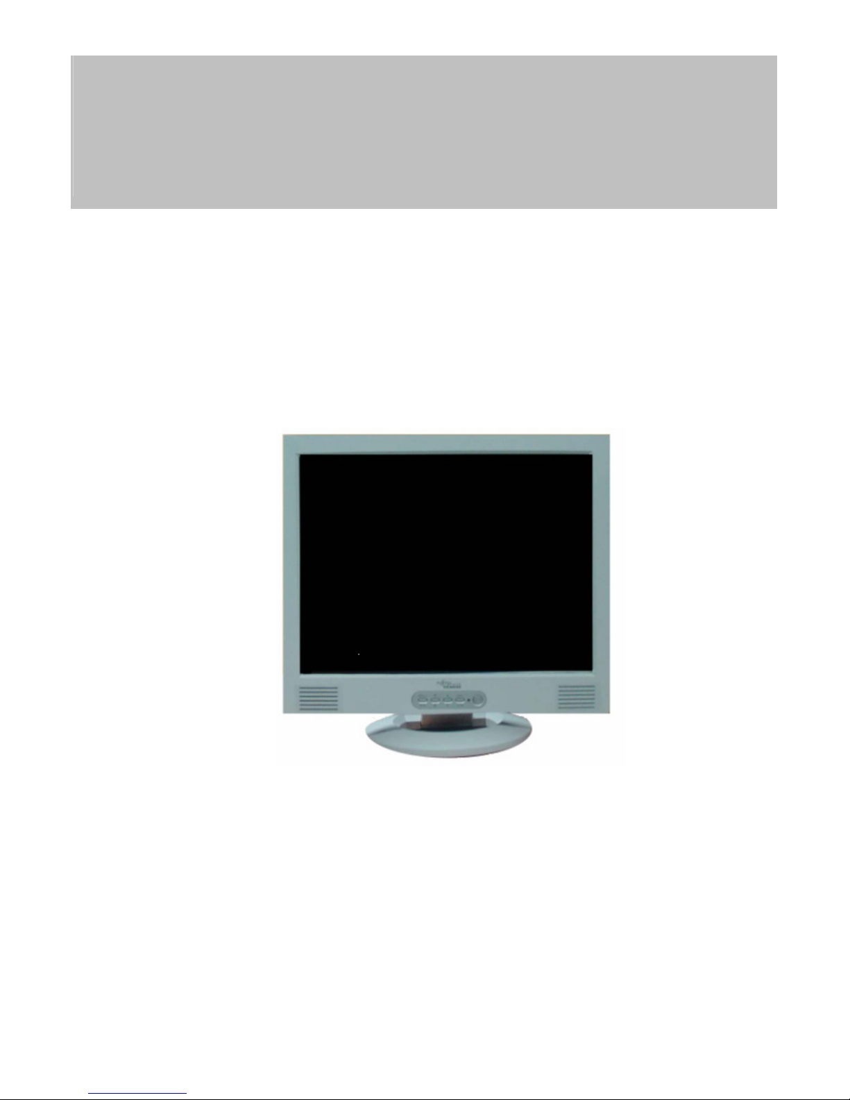
SERVICE MANUAL
15” LCD Monitor
FSC B15-1A
THESE DOCUMENTS ARE FOR REPAIR SERVICE INFORMATION ONLY. EVERY REASONABLE
EFFORT HAS BEEN MADE TO ENSURE THE ACCURACY OF THIS MANUAL; WE CANNOT
GUARANTEE THE ACCURACY OF THIS INFORMATION AFTER THE DATE OF PUBLICATION AND
DISCLAIMS RE LIABILITY FOR CHANGES, ERRORS OR OMISSIONS.
Page 2

FSC B15-1A Service Manual
2
Table of Contents
Table of Contents ---------------------------------------------------------------------------- 02
Revision List ----------------------------------------------------------------------------------- 03
1. Monitor Specification ---------------------------------------------------------------------04
2. LCD Monitor Description ---------------------------------------------------------------05
3. Operation Instructions --------------------------------------------------------------------06
3.1 General Instructions ------------------------------------------------------------------06
3.2 Control Button -------------------------------------------------------------------------06
3.3 Adjusting The Picture ----------------------------------------------------------------07
4. Input/Output Specification ---------------------------------------------------------------10
4.1 Input Signal Connector --------------------------------------------------------------10
4.2 Factory Preset Display Modes -----------------------------------------------------10
4.3 Power Supply Requirements -------------------------------------------------------11
4.3.1 Input Requirements ------------------------------------------------------------11
4.3.2 Output Requirements --------------------------------------------------------11
4.4 Panel Specification ---------------------------------------------------------------12
4.4.1 Panel Feature --------------------------------------------------------------------12
4.4.2 Display Characteristics ---------------------------------------------------------12
4.4.3 Optical Characteristics --------------------------------------------------------12
4.4.4 Parameter guide line for CCFL Inverter ------------------------------------13
5. Block Diagram -----------------------------------------------------------------------------13
5.1 Monitor Exploded View -------------------------------------------------------------13
5.2 Software Flow Chart ------------------------------------------------------------------14
5.3 Electrical Block Diagram -------------------------------------------------------------16
Page 3

FSC B15-1A Service Manual
3
5.3.1Main Board -----------------------------------------------------------------------16
5.3.2 Inverter/Power Board -----------------------------------------------------------17
6. Schematic -----------------------------------------------------------------------------------19
6.1 Main Board --------------------------------------------------------------------------19
6.2 Inverter/Power Board ----------------------------------------------------------------22
6.3 KeyPad Board -------------------------------------------------------------------------23
7. PCB Layout ---------------------------------------------------------------------------------24
7.1 Main Board -----------------------------------------------------------------------------24
7.2 Inverter/Power Board ----------------------------------------------------------------26
7.3 Keypad Board -------------------------------------------------------------------------27
8. Maintainability ------------------------------------------------------------------------------27
8.1 Equipments and Tools Requirements --------------------------------------------27
8.2 Trouble Shooting ----------------------------------------------------------------------28
8.2.1 Main Board -------------------------------------------------------------------------28
8.2.2 Power/Inverter Board ------------------------------------------------------------31
8.2.3 Key pad Board -------------------------------------------------------------------33
9. White-Balance, Luminance Adjustment ---------------------------------------------34
10. EDID Content ------------------------------------------------------------------------------35
11. BOM List ----------------------------------------------------------------------------36~50
Page 4
FSC B15-1A Service Manual
4
1. MONITOR SPECIFICATIONS
Driving system TFT Color LCD
Size 38.1cm(15.0")
Pixel pitch 0.297mm( H )x 0.297mm( V )
Viewable angle 130˚ (H) 90˚ (V)
LCD Panel
Response time (typ.) 25 ms
Video Analog
Sync. Type H/V TTL Separate and Composite Sync.
H-Frequency 30kHz – 61kHz
Input
V-Frequency 56-76Hz
Display Colors
Over 16 million Colors
Dot Clock
≦100MHz
Max. Resolution
1024 x 768
Plug & Play
VESA DDC2BTM
ON Mode
<35W
Power Consumption
OFF Mode
<1W
Maximum Screen Size
Horizontal : 12.0”(304.128mm)
Vertical : 9.0”(228.096mm)
Power Source
90~264VAC,47~63Hz
Environmental
Considerations
Operating Temp: 5°C to 40°C
Storage Temp.: -5°C to 40°C
Operating Humidity : 10% to 85%
Packaged 3.8Kgs Unit Weight (N. W.)
Unpackaged 5.5Kgs Unit
Page 5
FSC B15-1A Service Manual
5
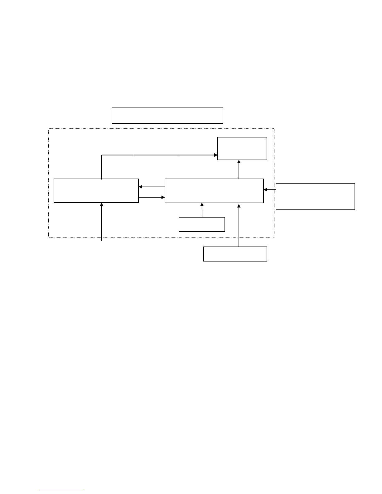
2. LCD MONITOR DESCRIPTION
The LCD MONITOR will contain an main board, an inverter/power board, keypad board and internal
adapter which house the flat panel control logic, brightness control logic and DDC.
The Inverter board will drive the backlight of panel and the DC-DC conversion.
The Adapter will provides the 12V DC-power to inverter/power board.
Power board
(
include: adapter, Inverter)
Flat Panel and
CCFL backlight
Main Board
Keyboard
RS232 Connector
For white balance
HOST Computer
CCFT Drive.
AC-IN
90V-264V
Video signal, DDC
Monitor Block Diagram
Page 6

FSC B15-1A Service Manual
6
3. OPERATING INSTRUCTIONS
3.1 GENERAL INSTRUCTIONS
Press the power button to turn the monitor on or off. The other control buttons are located at front panel
of the monitor. By changing these settings, the picture can be adjusted to your personal preferences.
-
The power cord should be connected.
-
Connect the video cable from the monitor to the video card.
-
Press the power button to turn on the monitor, the power indicator will light up.
3.2 CONTROL BUTTONS
-
Power Button:
When pressed, the monitor enters the off mode, and the LED turns blank. Press again to restore normal
status.
- Left / Right Button:
The Left/Right Button is used to control the monitor functions. Press to switch functions or adjust
settings.
- Auto Adjust Key:
The Auto Adjust Key is used to automatically set the H Position, V Position, Clock and Phase.
- Power Indicator:
Green — Power On mode.
orange — Power Saving mode.
Blank —Power Off Mode.
1.Buttons for the OSD menu
(On-Screen-display)
2.Power indicator
3.ON/OFF switch
Control Buttons
Page 7

FSC B15-1A Service Manual
7
3.3 ADJUSTING THE PICTURE
To set the OSD menu, perform the following steps:
Briefly press the SELCT/MENU button to activate the OSD menu.
The main menu appears on the screen with icons for the setting functions.
The first symbol (Brightness/Contrast) is highlighted.
necessary, press the 6 or 5 button to mark another icon (e.g. Image adjust).
Press the SELECT/MENU button to select the highlighted icon.
The corresponding setting window (here: Image Adjust) is displayed.
The first symbol (H-Position) is highlighted.
If necessary, press the 6 or 5 button to mark another function.
Press the SELECT/MENU button to select the highlighted function.
Press the 6 or 5 button to adjust the value for the selected function.
Press the EXIT/AUTO button to exit the function.
If necessary, press the button
6or 5to mark another function or press the EXIT/AUTO button to return to
the main menu.
All changes are stored automatically.
If you want to change other settings, select the corresponding function from the OSD main menu.
All possible adjustments of the main menu are described in the following.
Page 8

FSC B15-1A Service Manual
8
Adjusting the brightness and contrast
Calling the Brightness / Contrast setting window.
Brightness Setting the brightness of the display
With this function you change the brightness of the background
lighting.
Contrast Setting the contrast of the display
With this function you modify the contrast of bright colour tones.
Auto Level Setting the brightness of the display
With this function you can automatically set the contrast.
Adjusting size and position
Calling the Image adjust setting window
H-Position Adjusting the horizontal position
With this function you move the picture to the left or to the right.
V-Position Adjusting the vertical position
With this function you move the picture up or down.
Clock Setting synchronisation
With this function you adjust the picture width to eliminate vertical
picture disturbances.
Phase Eliminating picture interference
With this function you fine-tune your monitor to eliminate picture
interference.
Adjusting the volume
Calling the Audio setting window
Volume Setting the volume for playback with the integrated loudspeakers
Mute Switching the loudspeakers off or on
Setting colour temperature and colours
Calling the Colour setting window
Selecting the colour temperature
The "warmth" of the screen colours is set using the colour temperature.
The colour temperature is measured in K (= Kelvin). You can select
from 6500 K, 9300 K, Native and Custom Colour.
Page 9
FSC B15-1A Service Manual
9
Native = Original colour of the LCD display
Custom colour = Setting user-defined colours
In the user-defined setting you can change the colour ratios of the
basic colours (red, green, blue) as required.
Setting display of the OSD menu
Calling the OSD Setup setting window
Language Setting language for the OSD menu
With this function you choose between English (default setting),
French, German, Italian and Spanish as the language for the OSD
menu.
OSD
H-Position
Setting the horizontal position of the OSD menu
With this function you move the OSD menu to the left or to the right.
OSD
V-Position
Setting the vertical position of the OSD menu
With this function you move the OSD menu up or down.
OSD
Timeout
Setting the display duration of the OSD menu
With this function you select a value from 10 to 120 seconds.
If the set time expires without a setting being made, the OSD menu is
automatically faded out.
Setting functions in the "Advanced " menu
Calling the Advanced setting window
Resolution
Notifier
Displaying monitor data
The optimum resolution for this monitor is 1024 x 768 pixels. With the
function activated (On), a message appears on the screen after approx.
30 seconds if a different resolution is set.
Change the resolution to 1024 x 768 to achieve optimum picture quality.
With the function deactivated (Off), no message appears.
Factory
Recall
Activating the factory settings
With this function all settings are reset to the factory settings without
prompting for confirmation.
The Auto Processing message is displayed.
Displaying information
Calling the Information setting window
With this function the model designation, serial number, resolution, H/V
frequency, input signal and polarity of the synchronisation signal are
displayed.
Page 10
FSC B15-1A Service Manual
10
4. Input/Output Specification
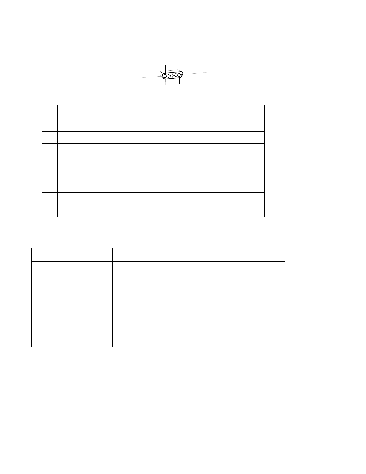
4.1 Input Signal Connector
Analog D-SUB Connector
1
5
6
10
11
15
Pin Meaning Pin Meaning
1 Video input red 9 +5 V (DDC)
2 Video input green 10 Sync. ground
3 Video input blue 11 Ground
4 Ground 12 DDC-Data
5 Ground 13 H. sync
6 Red video ground 14 V. sync
7 Green video ground 15 DDC Clock
8 Blue video ground
4.2 Factory Preset Display Modes
The following are the most frequently used of the preset operating modes:
Horizontal frequency Refresh rate Screen resolution
31.5 kHz
31.5 kHz
37.5 kHz
37.9 kHz
46.9 kHz
48.4 kHz
60.0 kHz
70 Hz
60 Hz
75 Hz
60 Hz
75 Hz
60 Hz
75 Hz
720 x 400
640 x 480
640 x 480
800 x 600
800 x 600
1024 x 768
1024 x 768
For ergonomic reasons, a screen resolution of 1024 x 768 pixels is recommended. Because of the
technology used (active matrix) an LCD monitor provides a totally flicker-free picture even with a refresh
rate of 60 Hz.
Page 11
FSC B15-1A Service Manual
11
4.3 Power Supply Requirements
4.3.1 Input Requirements
PARAMETER RANGE CONDITION
Input Voltage 90 to 264VAC RMS Universal input full range
Input Frequency 47 Hz to 63 Hz 110V AC 60Hz; 220V AC 50 Hz
Less than 2.0 Amps RMS
Input voltage 100 VAC RMS ; 60 Hertz.
Parameter must be reached within 3 seconds of
turn-on. Input Current
Less than 1.0 Amps RMS
Input voltage 220 VAC RMS ; 50 Hertz.
Parameter must be reached within 3 seconds of
turn-on.
Input Power Less than 75 Watts
Power factor > 0.5
Input voltage 120 VAC RMS ; 60
Hertz
Less than 30 A peak
Input voltage 100 VAC RMS ; 60 Hertz at all
Phase(0, 90, 180, 270 degree)
Inrush Current
Less than 50 A peak
Input voltage 240 VAC RMS ; 50 Hertz at all
Phase(0, 90, 180, 270 degree)
Input Fusing
Fuse should be located internal to
the adapter, easily accessible
when the cover is removed
Fuse must be UL/CSA approved. Fuse value
must no have to change for 115 VAC or 230 VAC
operation
Leakage Current Less than 3.5 mA Input voltage 240 Volts RMS ; 50 Hertz
Primary to secondary
1.5KVAC for 1 Minute(leakage current 10mA)
1.8KVAC for 1 Minute(leakage current 10mA)
3.0KVAC for 1 Minute(leakage current 10mA)
without Y-cap & Coupling cap.
Hi-Pot
Primary to Saft Ground
1.5KVAC for 1 Minute(leakage current 10mA)
1.8KVAC for 1 Minute(leakage current 10mA)
4.3.2 Output Requirements
PARAMETER RANGE CONDITION
DC Out 12VDC ± 5% Min 0A Max 3.75A
Load Regulation 12.0V(12.12V) ± 5% 11.4 to 12.6VDC
Dynamic Load
Regulation
Any frequency up to 250Hz(duty
50%)
±5% for 10% to 100%, 100% to 10% load
change for
+12Vdc
Ripple & noise 170mVpp at 12VDC Input voltage : 100VAC at 60Hz 240VAC at
50Hz
* Ripple and noise are measured.
Output current
protection
less than 7.0A, more than 12.0A
at 12.0VDC
Current exceeds maximum rateing more than
20%
Leakage Current Less than 0.25 mA Input voltage 100 Volts RMS ; 50 Hertz
Less than 0.5 mA Input voltage 240 Volts RMS ; 50 Hertz
Page 12
FSC B15-1A Service Manual
12
4.4 PANEL SPECIFICATION (SEC XH-L01)
4.4.1 Panel Feature
-High contrast ratio, high aperture structure
-Wide viewing angle
-High- speed response
-XGA (1024 x 768 pixels) resolution
-Display 16.2M colors
-Low power consumption
-4 CCFTS (Cold Cathode Fluorescent Tube)
-DE (Data Enable) only mode
-LVDS interface with 1 pixels/clock
4.4.2 Display Characteristics
Items Specification Unit
Display Area 304.1(H) x 228.1(V) (15.0 inch diagonal) mm
Driver element a-Si TFT active matrix
Display color 16.2M Colors
Number of pixels 1024 x 768 pixel
Pixel Arrangement RGB vertical stripe
Pixel pitch 0.297(H) x 0.297(W) mm
Display Mode Normally White
Surface treatment Haze 25, Anti-glare & Hard-Coating (3H)
4.4.3 Optical Characteristics
The optical characteristics are measured under stable conditions at 25℃ (Room Temperature):
Ta=25± 2℃, Voo=3.3V,fv=60Hz,fDCLK=65MHz,IL=6.0mArms
Item Symbol Conditions Min. Typ. Max. Unit Note
Contrast Ratio
(Center of screen)
C/R 200 300 -
(1)(2)(4)
Rising
Tr
- 5 -
Response
Time
Falling Tf - 20 -
msec (1)(3)
Luminance of White
(Center of screen)
YL 200 250 - Cd/m2
Rx 0.598 0.628 0.658
Red
Ry 0.323 0.353 0.383
Gx 0.260 0.290 0.320
Green
Gy 0.565 0.595 0.625
Bx 0.114 0.144 0.174
Blue
By 0.058 0.088 0.118
Wx 0.274 0.304 0.334
Color
Chromaticity
(CIE 1931)
White
Wy
ψ=0
θ=0
Normal
Viewing
Angle
0.295 0.325 0.355
ΘL
65 70 -
Hor
ΘR
65 70 -
ψH
50 55 -
Degree
s
Viewing Angle
Ver
ψL
CR≧10
55 60 -
(1)(4)
Brightness Uniformity BUNI - - 28
% (5)
Page 13
FSC B15-1A Service Manual
13
4.4.4 Parameter guide line for CCFL Inverter
The back-light system is an edge-lighting type with 4 CCFTS (Cold Cathode Fluorescent Tube)
The characteristics of two lamps are shown in the following tables
Ta =2 5± 2℃
ITEM SYMBOL MIN TYP MAX UNIT NOTE
Lamp Current IL 3.0 6.0 6.5 mArms (1)
Lamp Voltage VL - 665 - Vrms
IL=6.0
mArms
Frequency fL 40 - 60 KHz (2)
1220(25℃)
Startup Voltage Vs - -
1710(0℃)
Vrms (3)
Note: The inverter must have a symmetric output voltage waveform and be designed on the basis of the
modularized lamp.
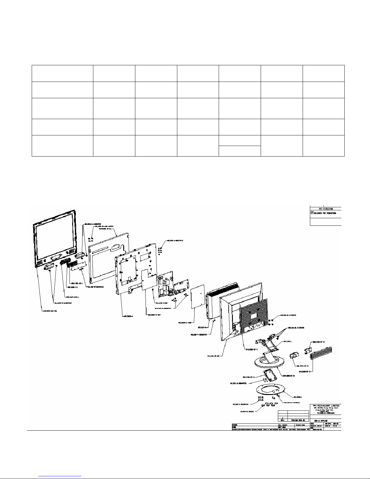
5. Block Diagram
5.1 Monitor Exploded View
Page 14

FSC B15-1A Service Manual
14
Page 15
FSC B15-1A Service Manual
15
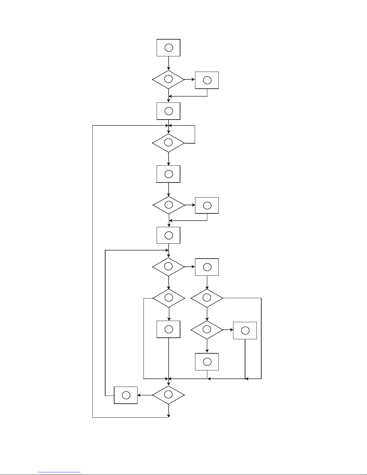
5.2 Software Flow Chart
1
2
5
10
12
7
643
8
9
141113
1516
1719
18
Page 16

FSC B15-1A Service Manual
16
1) MCU initialize.
2) Is the eeprom blank ?
3) Program the eeprom by default values.
4) Get the PWM value of brightness from eeprom.
5) Is the power key pressed ?
6) Clear all global flags.
7) Are the AUTO and SELECT keys pressed ?
8) Enter factory mode.
9) Save the power key status into eeprom.
Turn on the LED and set it to green color.
Scaler initialize.
10) In standby mode ?
11) Update the life time of back light.
12) Check the analog port, are there any signals coming ?
13) Does the scalar send out a interrupt request ?
14) Wake up the scalar.
15) Are there any signals coming from analog port ?
16) Display "No connection Check Signal Cable" message. And go into standby mode afte
r
the message disappear.
17) Program the scalar to be able to show the coming mode.
18) Process the OSD display.
19) Read the keyboard. Is the power key pressed ?
Page 17

FSC B15-1A Service Manual
17
5.3 Electrical Block Diagram
5.3.1 Main Board
Page 18

FSC B15-1A Service Manual
18
5.3.2 Inverter/Power Board
Inverter Block Diagram
Page 19

FSC B15-1A Service Manual
19
Power Block Diagram
Page 20

FSC B15-1A Service Manual
20
6. Schematic
6.1 Main Board
VAA4
B3
6.MCU
onBACKLITE
ST_DET2
onPANEL_5V/3.3V
SDA
INT
CSZ
DDC_DAT
ST_DET1
SCL
HWRESET
DDC_CLK
VCPU
RXD
TXD
AD0
AD1
AD2
AD3
AUDIO_SD
EAR_L
EAR_R
OUT_L
OUT_R
B2
4.SCALER
RIN
GIN
SOG
BIN
GNDR
GNDG
GNDB
HSYNC
VSYNC
R+
R-
G-
G+
B+
BCLK+
CLK-
CSZ
SCL
SDA
HWRESET
INT
VOLUME
AdjBACKLITE
PA[0..9]
VCC2.5
VCC3.3
VAA1
VAA2
VAA3
VAA4
AD0
AD1
AD2
AD3
PB[0..9]
VAA3
PB[0..9]
VLCD
B6
7.AUDIO
VOLUME
AUDIO_SD
VCC12V
EAR_L
EAR_R
OUT_L
OUT_R
VCC3.3
VCPU
TOP
B
MST8031B for AOC
B
17
星期一, 八月
25, 2003
Title
Size Document Number Rev
Date: Sheet
of
B4
2.POWER
onPanel_5V/3.3V
onBACKLITE
AdjBACKLITE
VCC3.3
VCC2.5
VAA1
VAA2
VAA3
VAA4
VCC12V
VLCD
VCPU
VLCD
B5
5.PANEL INTERFACE
VLCD
PA[0..9]
PB[0..9]
VCC2.5 VCC3.3
VAA4
B1
3.INPUT
RIN
GIN
BIN
VSYNC
GNDR
GNDG
GNDB
ST_DET1 HSYNC
SOGDDC_CLK
DDC_DAT
ST_DET2
R+
R-
G-
G+
B+
B-
CLK+
CLK-
TXD
RXD
VCC2.5
VAA3VAA1
VCC12V
VAA2
VCC12V
62X115 FOR SEIMENS
PA[0..9]
MST8031B SCHEMATIC
VCPU
VAA2
VAA1
DIM
VCC12V
+
C213
47uF/16V
R204
10K 1/16W
GND
R211
10K 1/16W
D201 DIODE SCHOTTKY
R208
10K 1/16W
VAA3 4
GND
VCC5V
R205 4.7K 1/16W
VCC5V+
FB201
600 OHM
R201 4.7K 1/16W
Brightness
+
C211
47uF/16V
VCC2.5 4
VCC5V
VAA3
VCC3.3
R206
10K 1/16W
C216
0.1uF
+
C209
47uF/16V
VCPU
VAA2 4
ON_OFF
+
C215
47uF/16V
C207
0.1uF
R209
NC
VCPU 6
C205
0.1uF
R210
0 1/16W
D202
DIODE
SOT-223
VAA1
Q204
PMBS3904
32
1
C212
0.1uF
R203
1K 1/16W
VLCD
VAA1 4
R212 4.7K 1/16W
C210
0.1uF
U202
AIC1117-33CY
1
23
ADJ
VOUTVIN
+
C206
1uF/0805
R202
10K 1/16W
VCC5V
+
C202
150uF/25V
Q203
AO3401
+
C204
150uF/25V
onBACKLITE 6
VLCD 5
Q202
PMBS3904
32
1
SOT-223
VCC5V
GND
Q201
PMBS3904
32
1
VCC2.5
VCC5V
+
C208
10uF/16V
onPanel_5V/3.3V6
C201
0.1uF
U201
RT9164-25CG
3 2
1
VI VO
GND
VCC5V
VAA2
VCC12V 7
GND
AdjBACKLITE4
VCC12V
GND
VCC12V
VAA4
VCC5V
GND
CN201
CONN
2
4
6
8
10
12
1
3
5
7
9
11
VCC3.3 4
VCC5V+
VCC5V+
C214
0.1uF
C203
0.1uF
VCC3.3
R207 4.7K 1/16W
VAA4 4
Page 21

FSC B15-1A Service Manual
21
C301
NC
C312
220pF
C315
0.1uF NC
D309
BAV99 NC
3
1
2
C304 0.047uF
R314
10K 1/16W
D320
MLL5232B 5.6V
VSYNC 4
DVI5V
R311 1K 1/16W
D304
BAT54C-GS08
3
1
2
G+ 4
R320 100 1/16W NC
CLK_DDC2
D310
BAV99 NC
3
1
2
VCC5V
DAT_DDC
D306
BAV99 NC
3
1
2
R+ 4
R326
75 1/16W
C310 0.047uF
R321
10K 1/16W NC
BIN 4
FB303 0 1/16W
C309 0.047uF
D301
BAV99
3
1
2
R322 100 1/16W NC
C313
0.1uF
D312
BAV99 NC
3
1
2
CLK+ 4
DVI5V
C314
0.1uF NC
HSI
C308 0.047uF
D317
MLL5232B 5.6V
R324
20K 1/16W NC
GIN 4
ST_DET2 6
PC5V
VSI
CLK- 4
D307
BAV99 NC
3
1
2
VCC5V
R317
20K 1/16W
D308
BAV99 NC
3
1
2
D318
MLL5232B 5.6V
CLK_DDC
U302
AT24C02N-10SC NC
1
2
3
45
6
7
8
A0
A1
A2
GNDSDA
SCL
WP
VCC
D303
BAV99
3
1
2
B+ 4
R313
2.2K 1/16W
R307 100 1/16W
D319
MLL5232B 5.6V
R310 150 1/16W
D302
BAV99
3
1
2
DAT_DDC2
RIN 4
SOG 4
VCC5V
CN301
DB15
1
6
2
7
3
8
4
9
5
11
12
13
14
15
10
TXD 6
VCC5V
R304 470 1/16W
D315
LL5232B 5.6V 5% NC
C311
33pF
C306 0.047uF
FB302 0 1/16W
RXD 6
D314
LL5232B 5.6V 5% NC
HSYNC 4
R302 100 1/16W
DDC_CLK6
CN302
JACK NC
1
2
3
4
5
6
7
8
25
28
9
10
11
12
13
14
15
16
26
29
17
18
19
20
21
22
23
24
27
DAT2-
DAT2+
2/4shield
DAT4-
DAT4+
DDC SCL
DDC SDA
VSYNC
R
HSYNC
DAT1-
DAT1+
1/3shield
DAT3-
DAT3+
+5V
SYNC GND
HPD
G
RGB GND
DAT0-
DAT0+
0/5shield
DAT5-
DAT5+
clk shield
clk+
clk-
B
R323
20K 1/16W NC
R303 100 1/16W
FB304 150 OHM
C307 0.001uF
D305
BAT54C-GS08 NC
3
1
2
ST_DET1 6
DDC_DAT6
FB301 0 1/16W
INPUT
B
MST8031B for AOC
B
37
星期一, 八月
25, 2003
Title
Size Document Number Rev
Date: Sheet
of
R306 100 1/16W
PC5V
R325
75 1/16W
D311
BAV99 NC
3
1
2
D321
MLL5232B 5.6V
R308
10K 1/16W
R318
20K 1/16W
GNDB 4
R305 100 1/16W
G- 4
C303
NC
R315 100 1/16W
R309 100 1/16W
R301 100 1/16W
R319 100 1/16W NC
R316 100 1/16W
D316
LL5232B 5.6V 5% NC
D313
BAV99 NC
3
1
2
C305 0.047uF
R312 100 1/16W
GNDG 4
B- 4
U301
AT24C02N-10SC
1
2
3
45
6
7
8
A0
A1
A2
GNDSDA
SCL
WP
VCC
VCC5V
VGA_CON
C302
NC
R327
75 1/16W
GNDR 4
R- 4
VPLL
PA2
PA9
PB[0..9]
PB0
C406
0.1uF
PA5
B-3
PB5
C401
0.1uF
RIN3
C413
0.1uF
NC
VAD
R404
10K
C421
0.1uF
R403 390 1/16W
VAA12
PB[0..9]
C430
100pF
BIN3
PA8
B+3
FB404
600 OHM
PA1
C409
0.1uF
C426
0.1uF
C412
0.1uF
C408
0.1uF
G+3
SOG3
VAA4
VAD
PB8
R407
10K
CLK+3
VCC5V
PA0
R409
10K 1/16W
+
C419
10uF/16V
NC
PA[0..9] 5
R402
4.7K 1/16W
R401
NC
C411
0.1uF
C416
0.1uF
VDPLL
PA3
FB405
600 OHM
VAA32
HWRESET6
4.7K
PB6
INT6
AD3 6
VPLL
R405
10K
SDA6
R408
1K 1/16W
C403 22pF
Direct Bus
PB3
AD2 6
HSYNC3
VDPLL
C415
0.1uF
VAA22
G-3
+
C427
10uF/16V
R402
PB2
AD1 6
C420
0.1uF
PA7
AdjBACKLITE2
VDD
PB7
C425
0.1uF
CLK-3
AD0 6
4.7K
R406
10K
C429
1uF
GNDB3
VCC3.3
GNDR3
VAA1
VPO
PB4
PA4
C402 22pF
PB9
C417
0.1uF
SCL6
VDVI
PA[0..9]
+
C422
10uF/16V
3-WIRE
SCALER
B
MST8031B for AOC
B
47
星期一, 九月
15, 2003
Title
Size Document Number Rev
Date: Sheet of
R+3
CSZ6
VAA3
+
C405
10uF/16V
FB403
600 OHM
C410
0.1uF
R401
X401
14.318MHz
+
C424
10uF/16V
VDVI
C428
0.1uF
VSYNC3
U401
MST8031/8131
63
60
61
58
62
59
57
37
38
40
41
43
44
46
47
49
50
52
66
67
69
70
71
32
72
73
74
107
55354535111218494
104
114
126188797117
3956362544210208595115
127198696105
116
33
34
108
109
110
111
112
113
118
119
120
121
122
123
124
125
128
1
29
28
30
31
53
65
64
48
106
103
102
68
77
78
6
RIN0
GIN0
SOGIN0
BIN0
RIN0M
GIN0M
BIN0M
HSYNC0
VSYNC0
R+
RG+
GB+
BCK+
CKREXT
REFP
REFM
CSZ
SDA
SCL
HWRESETZ
INT
PWM0
PWM1
LVACKM
AVDD
AVDD_MPLL
AVDD_DVI
BYPASS
AVDD_DVI
VDDP
VDDP
VDDP
VDDP
VDDP
VDDP
VDDP
VDDC
VDDC
VDDC
VDDC
AVSS_DVI
AVSS
AVSS_MPLL
AVSS_LPLL
AVSS_PLL
AVSS_DVI
GNDP
GNDP
GNDP
GNDP
GNDP
GNDP
GNDC
GNDC
GNDC
GNDP
GNDC
XIN
XOUT
LVA2P
LVA2M
LVA1P
LVA1M
LVA0P
LVA0M
NC/LVB3P
NC/LVB3M
NC/LVBCKP
NC/LVBCKM
NC/LVB2P
NC/LVB2M
NC/LVB1P
NC/LVB1M
NC/LVB0P
NC/LVB0M
DDC1_CLK/GPO8
DDC1_DAT/GPO7
ADO/NC
AD3/NC
AVDD_PLL
AVDD
AVSS
AVSS_DVI
LVACKP
LVA3M
LVA3P
AVSS
AD1/NC
AD2/NC
BUS TYPE/NC
VDVI
C418
0.1uF
VAA2
PB1
VAA42
R-3
C404 0.1uF
VOLUME7
GNDG3
PA6
C407
0.1uF
GIN3
C423
0.1uF
FB406
600 OHM
VCC5V
+
C414
10uF/16V
Page 22

FSC B15-1A Service Manual
22
LVB1M
LVA1M
PA4
RXEC+
PA[0..9]
RXO1+
LVB0P
PA7
VLCD
C510
0.1uF
LVACKP
LVB3P
RXE0-
LVB1P
RXE3-
PB8
PB0
LVB0P
VLCD 2
LVA0M
RXO2-
PB9
C511
0.1uF
LVA2M
RXE3+
LVB2M
PB[0..9]
LVBCKM
RXOC+
LVA3P
PA2
LVBCKP
LVB2P
RXEC-
PB3
LVBCKP
PA6
PB2
LVACKM
LVA0P
LVA3M
RXE0+
CN503
CON24A(PITCH 2.0)
1
3
5
7
9
11
13
15
17
19
21
23
2
4
6
8
10
12
14
16
18
20
22
24
RXOC-
LVACKM
RXE2-
PA1
LVA2P
RXO0-
RXO2+
LVB1P
LVBCKM
PA3
LVA2M
LVB2P
PA5
LVB0M
LVA0P
PB6
LVACKP
PB4
RXO0+
PA8
LVB2M
PB[0..9]
RXO3-
PA[0..9]4
RXE1-
PB5
LVB3M
LVA3P
LVB3M
LVA0M
RXO3+
+
C509
22uF/16V
LVA1M RXE1+
PB1
LVB1M
LVA3M
PA0
PA9
LVB3P
RXE2+
LVA1P
PB7
LVB0M
PANEL INTERFACE
B
MST8031B for AOC
A
57
星期一, 八月
25, 2003
Title
Size Document Number Rev
Date: Sheet
of
LVA2P
RXO1-
LVA1P
R616
4.7K 1/16W
R605 10K 1/16W
VCPU2
VCPU
LED_O
R623 0 1/16W
R609 100 1/16W
AUTO
RP601
10K 1/16W
123
4
876
5
R621 0 1/16W
+
C603
10uF/16V
R608 100 1/16W
R620 0 1/16W
R607 10K 1/16W
EAR_R
R602
10K 1/16W
EAR_R 7
Q602
PMBS3906
3 2
1
R601
10K 1/16W
C601
0.1uF
R615 10K 1/16W
D601
LL4148
DDC_CLK 3
LED_O
C608
0.001uF
CN603
NC
1
2
3
4
R619
4.7K 1/16W
C610
0.001uF
C607
0.001uF
RP602
10K 1/16W
123
4
876
5
R622 0 1/16W
MENU
R611 NC
AUDIO_SD7
R626 10K 1/16W
R612
NC
C612
0.1uF
R639
10K 1/16W
R617
470 1/16W
HWRESET 4
C602
22pF
C605
0.1uF
TXD 3
POWER
POWER
EAR_L
R635 100 1/16W
R603
10K 1/16W
R638
10K 1/16W
AD2 4
AD1 4
U602
24C16
1
2
3
4 5
6
7
8
A0
A1
A2
GND SDA
SCL
WP
VCC
SCL 4
AD0 4
VCPU
U601
W78E65P-40
35
21
20
10
14
15
16
17
2
3
4
5
6
7
8
9
43
42
41
40
39
38
37
36
24
25
26
27
28
29
30
31
19
18
32
33
13
11
22 44
12
EA/VP
XTAL1
XTAL2
RESET
INT0/P3.2
INT1/P3.3
T0/P3.4
T1/P3.5
P1.0
P1.1
P1.2
P1.3
P1.4
P1.5
P1.6
P1.7
P0.0
P0.1
P0.2
P0.3
P0.4
P0.5
P0.6
P0.7
P2.0
P2.1
P2.2
P2.3
P2.4
P2.5
P2.6
P2.7
P3.7/RD
P3.6/WR
PSEN
ALE/P
P3.1/TXD
P3.0/RXD
VSS VCC
P4.3
RXD 3
OUT_L
LED_GRN
Y601
20MHz
R618
470 1/16W
DDC_DAT 3
onPANEL_5V/3.3V 2
MENU
AD3 4
LEFT
VCPU
R613
10K 1/16W
Q601
PMBS3906
3 2
1
C613
0.1uF
OUT_R
CSZ 4
VCPU
ST_DET13
OUT_L7
R640 10K 1/16W
RIGHT
R637
10K 1/16W
R634 100 1/16W
LED_G
onBACKLITE 2
MPU
B
MST8031B for AOC
B
67
星期三, 十月
29, 2003
Title
Size Document Number Rev
Date: Sheet
of
R604 10K 1/16W
AUTO
VCPU
R624 0 1/16W
INT4
C604
22pF
ST_DET23
R610 NC
EAR_L7
CN602
CONN
2
4
6
8
10
12
14
1
3
5
7
9
11
13
SDA 4
RIGHT
R606 10K 1/16W
C606
0.001uF
LED_G
LED_ORANGE
LEFT
VCPU
C609
0.001uF
OUT_R 7
Page 23

FSC B15-1A Service Manual
23
C706 0.47uF/16V
VCC12V
C712
100pF
VOL
C710
1uF
C711
100pF
R712
220K 1/16W
AUDIO_SD6
R709
75 1/16W
OUT_R 6
R708
1K 1/16W
R704 100 1/16W
CN701
PHONEJACK
MUTE
R707
1K 1/16W
OUT_L 6
+
C705 470uF/16V
1
+
C707 470uF/16V
+
C701
470uF/16V
VOLUME 4
5
EAR_R 6
R703
10K 1/16W
4
C704 0.47uF/16V
C713
0.1uF/16V
3
U701
TDA7496L
123
4
5
6
7
8
9
10
11
12
13
14
15
16
17
181920
GND
GND
GND
INL
VAROUT_L
VOLUME
VAROUT_R
NC
INR
SVR
STBY
MUTE
GND
OUTR
VS
VS
OUTL
GND
GND
GND
C703
0.1uF/16V
EAR_L 6
R702
75 1/16W
C709
1uF
2
R706 100 1/16W
R711
5.6K 1/16W
R701 10K 1/16W
R710
5.6K 1/16W
D702
LL4148
D701
LL4148
+
C708
470uF/16V
VCC12V2
+
C702
470uF/16V
R705
10K 1/16W
6.2 Inverter/Power Board
R902
1M 1/16W
Q903
2SK2996
SG6841
IC901
SG6841
13
4
72
56
8
R908
10 1/4W
CN901
12
3
GND
3.3V
L903
FB903
0 1/16W
R904
1M 1/4W
C913
0.0022uF/250V
GND
R912
100 1/16W
C931
0.1uF
C927
0.1uF
C920
0.001uF/500V
C912
N.C
D910 31DQ10
R909
4.7K 1/16W
R901
1M 1/16W
R907
1M 1/4W
C903 0.1uF/250V
5V
C921
0.001uF/500V
F902
0 1/16W
D911 31DQ10
R933
150 1/16W
D903
1N4148
IC902
PC123FY2 4P
12
43
IC905 AIC1084-33CT
3
1
2
VIN
ADJ
Vout
CN102
CONN
1
2
3
4
5
6
R930
470 1/4W
R927
1K 1/4W
F901
FUSE
3.3V
D912 31DQ06
Q901
2PA733P
R920
47 1/2W
L902
1 4
2 3
C911
0.001uF
P901A
Wire Harness
1
2
R914
N.C/0603
-+
DB901
2KBP06M
1
4
3
2
+
C925
1000uF/16V
C902
0.001uF/250V
ZD904
SML4736
C909
0.1uF
+
C929
470uF/16V
FB904
0 1/16W
L901
2 3
1 4
+
C922
1000uF/16V
D901
UF4007
R929
JUMPER
12
D913 31DQ06
C904 0.47uF/250V
C928
0.1uF
R905
1M 1/4W
D905
1N4148
12V
R915
10K 1/16W
t
NR901
NTCR
TO INVERTER
R937
0.56 2W
ZD903
HZ5C1
R928
1K 1/4W
L904
C936
0.1uF
R918
20K 1/4W
C901
0.001uF/250V
R911
4.7K 1/16W
D904
1N4148
R916
24K 1/10W
+
C930
470uF/16V
+
C907
10uF
FB901
BEAD
C908
0.1uF
ZD902
HZ12B2
D902
PS102R
R926
2.4K 1/4W
R913
N.C_0603
FB902
O
O
O
T901
1
9
3
5
4
7,8
7,8
10,11
C906
0.0015uF/2KV
IC903
HTL431
C910
0.1uF
ZD901
RLZ20B
R903
100K 2W
R925
18K 1/4W
R919
0.39 2W
R922
47 1/4W
Q902
2PC945P
C935
0.01uF
+
C905
120uF/400V
R932
N.C
71511013-B 1
POWER / INVERTER / AUDIO
B
13Tuesday, October 01, 2002
<Title>
Size Document Number Rev
Date: Sheet
of
+
C926
470uF/16V
R924
11K 1/4W
R917
JUMPER
12
R910
4.7K 1/16W
R931
1K 1/16W
R906
1M 1/4W
+
C924
470uF/16V
Page 24

FSC B15-1A Service Manual
24
R212
3.9K
R213
3.9K
R241
51K
+12V
CN204
1
2
R226
2K 1/16W
is power GND
R203
10K
D203
RLZ11B
NO/OFF
R208
4.7K 1/16W
C213
0.22uF/100V
C218
22pF/3KV
Q209
2SC5706
1
23
C221
0.47uF/63V
R217
220 1/16W
Q208
MPS3906
3 2
1
C209
1uF/25V
C205
0.1uF
CN201
1
2
CN202
1
2
Q212
2SC5706
1
23
C208
330pF
R223
12K
R222
12K
TP5
HVL
1
PT201
POWER X'FMR
5 9
3,4
6
71
2
C217
22pF/3KV
+
C207
10uF
R230
2K
Q210
2SC5706
1
23
R209
4.7K 1/16W
R239
12K
U201
TL1451ACNSR
1234567
8 9
10111213141516
CTRT1IN+
1IN-
1FBK
1DTC
1OUT
GND Vcc
2OUT
2DTC
2FBK
2IN-
2IN+
SCP
REF
PT202
POWER X'FMR
5 9
3,4
6
71
2
R227
2K 1/16W
DIM
R224
2K
C224
1uF/25V
C206
0.1uF
R233
1K
D208
1N4148
D201
SR24
TP3
HVL
1
+
C223
150uF/25V
R216
220 1/16W
R220
15K
Q203 SI4431DY-T1
4
8
5
6
7
3
2
1
TP4
HVL
1
R201
30K
R214
3.9K 1/16W
R228
2K
R238
12K
R205
47K
R232
1K
TP2
HVO
1
C214
0.22uF/100V
R236
620
C220
1uF/25V
R235
910 1/4W
TP1
HVO
1
Q204 SI4431DY-T1
4
8
5
6
7
3
2
1
CN203
1
2
C210
1uF/25V
R202
10K
A
2. FOR SAMSUNG M170EU-L01 INVERTER
AOC (Top Victory) Electronics Co., Ltd.
B
22
Tuesday, October 01, 2002
Title
Size Document Number Rev
Date: Sheet of
R219
470
D204
RLZ11B
C225
1uF/25V
R221
15K
R240
51K
R215
3.9K 1/16W
R207
OPEN
R237
620
D205
1N4148
C203
1uF/25V
D202
SR24
C204
0.1uF
C212
1uF/25V
D206
1N4148
C222
0.47uF/63V
D209
1N4148
D207
1N4148
R204
10K
C202
0.1uF/25V
C216
22pF/3KV
R210
15K
TP6
HVL
1
Q205
MPS3904
R234
910 1/4W
R206
47K
R211
15K
Q211
2SC5706
1
23
C215
22pF/3KV
R218
470
C219
1uF/25V
Q206
MPS3904
is signal GND
Q201
DTC144WKA
L201
R229
2K
C211
1uF/25V
R225
2K
+
C201
150uF/25V
R231
2K
Q202
DTA144WKA
L202
D210
1N4148
Q207
MPS3906
3 2
1
6.3 Key Pad Board
KEY_LEFT_J
SW3
KEY RIGHT
SW2
KEY MENU
SPKR_R
J001
CONN
1 2
OUT_L+
KEY_AUTO
LED_GRN#
HP_L
OUT_R+
SW5
KEY AUTO
KEY_LEFT
CN3
CONN
1
2
SPKR_R+
LED_GRN#
DP1
LED
CN1
PHONEJACK
7
6
3
1
2
4
5
OUT_L+
KEY_MENU
GND
KEY_LEFT
HP_R
KEY_MENU
KEY RIGHT
KEY_LEFT_J
SW1
POWER KEY
J002
CONN
1 2
OUT_R+
HP_R
LCD_ONOFF
KEY_AUTO
CN4
CONN
1
2
CONTROL KEY PAD (Switch)
A
KEY PAD 715L1071-D
AOC (Top Victory) Electronics Co., Ltd.
A
11Thursday, January 09, 2003
Title
Size Document Number Rev
Date: Sheet
of
LCD_ONOFF
SW4
KEY LEFT
SPKR_L+
KEY_RIGHT
GND
HP_L
SPKR_R+
LED_ORG#
LED_ORG#
SPKR_L+
SPKR_R
CN2
CONN
2
4
6
8
10
12
14
1
3
5
7
9
11
13
Page 25

FSC B15-1A Service Manual
25
7. PCB Layout
7.1 Main Board
715L1225-C
Page 26

FSC B15-1A Service Manual
26
Page 27

FSC B15-1A Service Manual
27
7.2 Inverter/Power Board
715L1063-1A
Page 28

FSC B15-1A Service Manual
28
7.3 Keypad Board
715L1071-1-2
8. Maintainability
8.1 Equirement and Tools Requirement
1.)Voltmeter.
2.)Oscilloscope.
3) Pattern Generator.
4) DDC Tool with a IBM Compatible Computer.
5) Alignment Tool.
6) LCD Color Analyzer.
7) Service Manual.
8) User Manual.
Page 29

FSC B15-1A Service Manual
29
8.2 Trouble Shooting
8.2.1 Main Board
1.NO SCREEN APPEAR
Note: 1. if Replace “MAIN-BOARD” , Please re-do “DDC-content” programmed & “WHITE-Balance”.
2. if Replace “Power Board” only, Please re-do “ WHITE-Balance”
Measured U021 pin 2 =2.5 V?
Measured U202 pin 2= 3.3V?
Measured CN201
p
in 2 = 3.3V?
Check Correspondent component.
Is there any shortage or cold
Yes, all DC level exist
Disconnected the Signal cable( Loose the
Signal cable ),Is the screen show “No
Signal go to sleep ?
Replace U601
MCU
No, nothing is show
Connected the Signal cable again,
Check LED status.
Check Power switch is in
Power-on status , and check if
Power switch had been stuck ?
Led Orange
OK, Keyboard no stuck
Led orange
Led Green
Check the Wire-Harness from CN503 Measured RGB (R301,R302,R303)
H,V Input at R310,R311 was there
have signal ?
Check
Correspondent
component
short/open
( Protection Diode )
and Signal cable bad ?
NG
OK ,Wire tight enough
Check Panel-Power Circuit Block
OK, Panel Power
Check U401 Data-output Block
OK, U203 data OK
Replace Power board and Check
Inverter control relative circuit
Re-do White balance
OK , Input Normal
Measured Crystal X401(14.318MHz)
OK, clock normal
Replace U401 (MST8011B)
OK
No LED
Page 30

FSC B15-1A Service Manual
30
2.PANEL-POWER CIRCUIT
3.INVERTER Control Relative Circuit
check R207 should have response from 0V to 5V
When we switch the power switch from on to off
NG
Check on PANEL U601 PIN25
In normal operation, when LED =green, R207
should =0 v,
OK,R207 have response
NG, no Voltage
Measured the Q203 pin 3= 3.3 V?
Check CN201 pin 9,10= 5V
OK
OK
Replace Q203
Ye s
Measured the inverter connector CN201
Pin2 on/off control=5V (on)
Pin4 PWM signal control dim 0V-5V
NG
Check the adjust Back-lite relative circuit, R205
In normal operation, when LED =green,
R205 adjust Back-lite should =5 v,
If Bklt-On no-response when the power switch turn on-off,
Replace U401MST8011
NG, still no screen
Replace Power board to new-one,
Check the screen is normal ??
OK
Page 31

FSC B15-1A Service Manual
31
4.U401-DATA Output
NG , no transition
Replace MST8011B (U401) or
replace MAINBOARD.
Check U401MST8011B
Signal output
PA0~PA9, PB0~PB9
Is the waveform ok ?
If Main Board being replace ,
please do the DDC – content
OK
Page 32

FSC B15-1A Service Manual
32
8.2.2 Power/Inverter Board
1.) No power
Check to CN102 Pin9 and
pin10= 5V
Check Interface board
OK
NG
Check AC line volt 120V
or 220V
NG
OK
Change F901 , check BD901,Q903,IC901
Check the voltage of C904(+)
Check bridge rectified circuit
NG
OK
Check start voltage for the pin3 of IC901
Change IC901
NG
Repeating the start voltage
Check the auxiliary voltage is smaller than 20V
1) Check IC902, IC903
2) Check Q901,Q902…OVP circuit
NG
OK
Check R919, D910,D911,D912,D913, ZD904
Page 33

FSC B15-1A Service Manual
33
2.) W / LED , No Backlight
Check C201(+) =12V
NG
OK
Change F902
Check D201/Q209/Q210 or
D202/Q211/Q212
Check ON/OFF signal
Check Interface board
NG
OK
Check U201 pin9=12V
NG
OK
Change Q201 or Q202
Check the pin1 of U201 have sawtooth wave
NG
OK
Change U201
Check D201(-),D202(-) have the output of square wave at short time.
NG
OK
Check Q205/Q207/Q203/D201 or
Q206/Q208/Q204/D202
Check the resonant wave of pin2 & pin5 for PT201/PT202
NG
OK
Check the output of PT201/PT202
Check Q209/Q210/C213 or
Q211/Q212/C214
Check connecter & lamp
OK
NG
Change PT201or PT202
Page 34

FSC B15-1A Service Manual
34
8.2.3 KeyPad Board
OSD is unstable or not working
Is Key Pad Board connecting
normally ?
Connect Key Pad
Board
Is Button Switch normally ?
Replace Button
Switch
Y
N N
Is Key Pad Board Normally ?
Replace Key Pad
Board
Y
N
Y
Check Main Board
Page 35

FSC B15-1A Service Manual
35
9. White-Balance, Luminance adjustment
Approximately 30 minutes should be allowed for warm up before proceeding
White-Balance adjustment.
1.、How to do the Chroma-7120 MEM .channel setting
A、Reference to chroma 7120 user guide
B、Use “ SC” key and “ NEXT” key to modify xyY value and use “ID” key to modify the
TEXT description Following is the procedure to do white-balance adjust
2、Setting the color temp. you want
A、MEM.CHANNEL 4 ( 6500 color):
6500 color temp. parameter is x = 313±10, y = 329 ±10, Y = 180 ±10 cd/m2)
B 、MEN.CHANNEL 5 (9300 color):
9300 color temp. parameter is x = 283±10, y = 297 ±10, Y = 180 ±10 cd/m2)
3、Into factory mode of LCD B15-1A
A、Press MENU button during 2 seconds along with press Power button will activate the
factory mode, then MCU will do AUTO LEVEL automatically. Meanwhile press MENU
the OSD screen will located at LEFT TOP OF PANEL.
4、Bias adjustment :
Set the Contrast
to 50
Adjust the Brightness to 100.
5、Gain adjustment :
Move cursor to “-F-” and press MENU key
A、Adjust C2(9300) color-temperature
1、Switch the Chroma-7120 to RGB-Mode (with press “MODE” button )
2、Switch the MEM. channel to Channel 3 ( with up or down arrow on chroma 7120 )
3、The LCD-indicator on chroma 7120 will show x = 283 ±10, y = 297±10,
Y = 180 ±10 cd/m
2
4、Adjust the RED of color1 on factory window until chroma 7120 indicator reached
the value R=100
5、Adjust the GREEN of color1 on factory window until chroma 7120 indicator reached
the value G=100
6、Adjust the BLUE of color1 on factory window until chroma 7120 indicator reached
the value B=100
7、Repeat above procedure ( item 4,5,6) until chroma 7120 RGB value meet the
tolerance =100±2
Page 36

FSC B15-1A Service Manual
36
B、Adjust C1(6500) color-temperature
1、Switch the chroma-7120 to RGB-Mode (with press “MODE” button )
2、Switch the MEM .channel to Channel 4( with up or down arrow on chroma 7120 )
3、The LCD-indicator on chroma 7120 will show x = 313 ±10, y = 329 ±10,
Y = 180 ±10 cd/m2
4、Adjust the RED of color3 on factory window until chroma 7120 indicator reached
the value R=100
5、Adjust the GREEN of color3 on factory window until chroma 7120 indicator reached
the value G=100
6、Adjust the BLUE of color3 on factory window until chroma 7120 indicator reached
the value B=100
7、Repeat above procedure ( item 4,5,6) until chroma 7120 RGB value meet the
tolerance =100±2
C、Press reset key and Turn the Power-button “off to on” to quit from factory mode.
10. EDIT Content
D-SUB Connector(Analog)
x0 x1 x2 x3 x4 x5 x6 x7 x8 x9 xA xB xC xD xE xF
00 00 FF FF FF FF FF FF 00 1A B3 84 04 01 00 00 00
16: 2D 0D 01 03 68 1F 17 78 2A 57 84 A2 58 4E 93 24
32: 1A 50 53 A5 4E 00 61 40 61 4F 45 40 45 4F 31 40
48: 31 4F 01 01 01 01 64 19 00 40 41 00 26 30 18 88
64: 36 00 30 E4 10 00 00 18 00 00 00 FF 00 59 45 41
80: 55 30 30 30 30 30 31 0A 20 20 00 00 00 FD 00 37
96: 4B 1E 3F 08 00 0A 20 20 20 20 20 20 00 00 00 FC
112 00 42 31 35 2D 31 41 0A 20 20 20 20 20 20 00 8A
Note: Byte 0C, 0D, 0E, 0F means Serial No. Byte 10, 11 means Manufacture Time. Byte 7F means
checksum
Page 37

FSC B15-1A Service Manual
37
11. BOM List
T560KSXHBSM8A
CBPC560KSXM8 CONVERSION BOARD FOR T5 M 1 PCS
KEPC560KM3 KEY BOARD FOR T560K*SNI M 1 PCS
PWPC5425B1 POWER BOARD M 1 PCS
2L6008 1 SCREW P 4 PCS
7L 1 L 7 WOODEN PALLET P 0.007 PCS
7L 1 L 8 WOODEN PALLET P 0.007 PCS
15L5923 2 MAIN FRAME P 1 PCS
33L4703 BT L COVER HINGE L P 1 PCS
33L4704 BT L COVER HINGE R P 1 PCS
34L1283 EF B CONNECTOR COVER P 1 PCS
40L 150622 1 ID LABEL P 1 PCS
40L 152509 RECYCLE LABEL P 0 PCS
40L 152512 RECYCLE LABEL P 0 PCS
40L 457624 1B CPU LABEL P 1 PCS
40L 45762412A CBPC LABEL P 1 PCS
40L 581 26668 SLZ LABEL P 1 PCS
40L 581 26704 唛头纸 FOR CARTON/PALLET P 0.05 PCS
44L3548 1 EPS(L) P 1 PCS
44L3548 2 EPS(R) P 1 PCS
44L3548 5 U TYPE SHEET P 1 PCS
44L3548624 1A CARTON P 1 PCS
44L9003210 护角板 P 0.057 PCS
45L 76 28 RN PE BAG for MANUAL/BASE P 1 PCS
45L 77 3 打包膜 P 173 CM
45L 77500 BARCODE RIBBON P 19 CM
45L 77501 BARCODE RIBBON P 0.5 CM
45L 88607 PE BAG FOR MONITOR P 1 PCS
50L 600 2 HANDLE1 P 1 PCS
50L 600 3 HANDLE2 P 1 PCS
52L 1185 MIDDLE TAPE FOR CARTON P 100 CM
52L 1186 SMALL TAPE P 8 CM
52L6020 2 PROTECT FILM P 0 PCS
52L6025 11527 INSULATE SHEET P 1 PCS
52L6025 11528 INSULATE SHEET P 2 PCS
70L L15200 SM DRIVE DISK SIEMENS P 1 PCS
85L 637 2 SHIELD P 1 PCS
89L 173 56 11 AUDIO HARNESS P 1 PCS
89L 174L17 12 SIGNAL CABEL DB15-DB15 P 1 PCS
Page 38

FSC B15-1A Service Manual
38
89L404C18N IS POWER CORD 插墙 FOR EUROP P 1 PCS
95L8014 12 8 HARNESS P 1 PCS
95L8018 24 2 HARNESS 60mm GREATLAND P 1 PCS
M1L 140 10 47 SCREW M4X10 P 4 PCS
M1L 140 10 47 SCREW M4X10 P 4 PCS
M1L 330 4128 SCREW M3X4 P 2 PCS
M1L1030 10128 SCREW P 4 PCS
M1L1130 6128 SCREW P 9 PCS
M1L1140 5128 SCREW 4X6 P 1 PCS
Q1L 330 8120 SCREW 3X8mm P 3 PCS
Q1L 330 8120 SCREW 3X8mm P 7 PCS
705L560KB34077 LCD 后壳 ASS'Y X 1 PCS
750LLS50 XH SEC 15" PANEL(XH-L01) P 1 PCS
AIC560KSXM8 MAIN BOARD FOR T560K*SN M 1 PCS
CN602 33L380214H WAFER 14P RIGHT ANGLE P P 1 PCS
CN201 33L800912L H HEADER 2*6P P 1 PCS
CN503 33L801724A H PIN HEADER 24P 2.0mm P 1 PCS
40L 457624 1B CPU LABEL P 1 PCS
40L 45762412A CBPC LABEL P 1 PCS
44L3231508512 导电泡棉 P 1 PCS
U701 56L 616 1 TDA7496L BY ST P 1 PCS
U601 56L1125137SB5 W78E65P-40 P 1 PCS
C202 67L215B221 4H LOW ESR 220UF 25V 8*11 P 1 PCS
C204 67L215B221 4H LOW ESR 220UF 25V 8*11 P 1 PCS
C405 67L309L100 3 10UF +-20% 16V P 1 PCS
C414 67L309L100 3 10UF +-20% 16V P 1 PCS
C419 67L309L100 3 10UF +-20% 16V P 1 PCS
C422 67L309L100 3 10UF +-20% 16V P 1 PCS
C424 67L309L100 3 10UF +-20% 16V P 1 PCS
C427 67L309L100 3 10UF +-20% 16V P 1 PCS
C603 67L309L100 3 10UF +-20% 16V P 1 PCS
C208 67L309L101 3 100UF +-20% 16V P 1 PCS
C209 67L309L470 3 47UF +-20% 16V P 1 PCS
C211 67L309L470 3 47UF +-20% 16V P 1 PCS
C213 67L309L470 3 47UF +-20% 16V P 1 PCS
C215 67L309L470 3 47UF +-20% 16V P 1 PCS
C509 67L309L470 3 47UF +-20% 16V P 1 PCS
C701 67L309L471 3 470UF+-20% 16V P 1 PCS
C702 67L309L471 3 470UF+-20% 16V P 1 PCS
C705 67L309L471 3 470UF+-20% 16V P 1 PCS
Page 39

FSC B15-1A Service Manual
39
C707 67L309L471 3 470UF+-20% 16V P 1 PCS
C708 67L309L471 3 470UF+-20% 16V P 1 PCS
CN701 88L 30210K PHONE JACK P 1 PCS
CN301 88L 35315F HS D-SUB 15PIN FEMALE P 1 PCS
90L6059 1 散热片 FOR U701 P 1 PCS
X401 93L 22 53 CRYSTAL 14.318MHzHC-49U P 1 PCS
Y601 93L 22 55 CRYSTAL 20MHz HC-49US P 1 PCS
Y601 93L 22 55 H 20MHZ P 0 PCS
U401 56L 562 57 MST8011B P 1 PCS
U202 56L 563 7 AIC1084-33CM P 1 PCS
U201 56L 585 5 RT9164-25CG P 1 PCS
U301 56L1133 20 AT24C02N-10SC BY ATMEL P 1 PCS
U602 56L1133 24 AT24C16N-10SC-2.7 P 1 PCS
U301 56L1133 34 M24C02-WMN6T SMT P 0 PCS
U602 56L1133516 M24C16-WMN6T P 0 PCS
Q201 57L 417 4 PMBS3904/PHILIPS-SMT(04 P 1 PCS
Q202 57L 417 4 PMBS3904/PHILIPS-SMT(04 P 1 PCS
Q204 57L 417 4 PMBS3904/PHILIPS-SMT(04 P 1 PCS
Q601 57L 417 6 PMBS3906/PHILIPS-SMT(06 P 1 PCS
Q602 57L 417 6 PMBS3906/PHILIPS-SMT(06 P 1 PCS
Q203 57L 763 1 A03401 SOT23 BY AOS(A1) P 1 PCS
RP601 61L 125103 8 CHIP AR 8P4R 10KOHM +-5 P 1 PCS
RP602 61L 125103 8 CHIP AR 8P4R 10KOHM +-5 P 1 PCS
FB301 61L0603000 CHIPR 0OHM +-5% 1/16W P 1 PCS
FB302 61L0603000 CHIPR 0OHM +-5% 1/16W P 1 PCS
FB303 61L0603000 CHIPR 0OHM +-5% 1/16W P 1 PCS
R210 61L0603000 CHIPR 0OHM +-5% 1/16W P 1 PCS
R301 61L0603101 CHIPR 100 OHM +-5% 1/16 P 1 PCS
R302 61L0603101 CHIPR 100 OHM +-5% 1/16 P 1 PCS
R303 61L0603101 CHIPR 100 OHM +-5% 1/16 P 1 PCS
R305 61L0603101 CHIPR 100 OHM +-5% 1/16 P 1 PCS
R306 61L0603101 CHIPR 100 OHM +-5% 1/16 P 1 PCS
R307 61L0603101 CHIPR 100 OHM +-5% 1/16 P 1 PCS
R309 61L0603101 CHIPR 100 OHM +-5% 1/16 P 1 PCS
R312 61L0603101 CHIPR 100 OHM +-5% 1/16 P 1 PCS
R315 61L0603101 CHIPR 100 OHM +-5% 1/16 P 1 PCS
R316 61L0603101 CHIPR 100 OHM +-5% 1/16 P 1 PCS
R319 61L0603101 CHIPR 100 OHM +-5% 1/16 P 1 PCS
R320 61L0603101 CHIPR 100 OHM +-5% 1/16 P 1 PCS
R322 61L0603101 CHIPR 100 OHM +-5% 1/16 P 1 PCS
Page 40

FSC B15-1A Service Manual
40
R608 61L0603101 CHIPR 100 OHM +-5% 1/16 P 1 PCS
R609 61L0603101 CHIPR 100 OHM +-5% 1/16 P 1 PCS
R634 61L0603101 CHIPR 100 OHM +-5% 1/16 P 1 PCS
R635 61L0603101 CHIPR 100 OHM +-5% 1/16 P 1 PCS
R704 61L0603101 CHIPR 100 OHM +-5% 1/16 P 1 PCS
R706 61L0603101 CHIPR 100 OHM +-5% 1/16 P 1 PCS
R204 61L0603102 CHIPR 1K OHM +-5% 1/16W P 1 PCS
R310 61L0603102 CHIPR 1K OHM +-5% 1/16W P 1 PCS
R311 61L0603102 CHIPR 1K OHM +-5% 1/16W P 1 PCS
R408 61L0603102 CHIPR 1K OHM +-5% 1/16W P 1 PCS
R707 61L0603102 CHIPR 1K OHM +-5% 1/16W P 1 PCS
R708 61L0603102 CHIPR 1K OHM +-5% 1/16W P 1 PCS
R202 61L0603103 CHIPR 10K OHM +-5% 1/16 P 1 PCS
R206 61L0603103 CHIPR 10K OHM +-5% 1/16 P 1 PCS
R208 61L0603103 CHIPR 10K OHM +-5% 1/16 P 1 PCS
R211 61L0603103 CHIPR 10K OHM +-5% 1/16 P 1 PCS
R308 61L0603103 CHIPR 10K OHM +-5% 1/16 P 1 PCS
R321 61L0603103 CHIPR 10K OHM +-5% 1/16 P 1 PCS
R404 61L0603103 CHIPR 10K OHM +-5% 1/16 P 1 PCS
R405 61L0603103 CHIPR 10K OHM +-5% 1/16 P 1 PCS
R406 61L0603103 CHIPR 10K OHM +-5% 1/16 P 1 PCS
R407 61L0603103 CHIPR 10K OHM +-5% 1/16 P 1 PCS
R409 61L0603103 CHIPR 10K OHM +-5% 1/16 P 1 PCS
R601 61L0603103 CHIPR 10K OHM +-5% 1/16 P 1 PCS
R602 61L0603103 CHIPR 10K OHM +-5% 1/16 P 1 PCS
R603 61L0603103 CHIPR 10K OHM +-5% 1/16 P 1 PCS
R604 61L0603103 CHIPR 10K OHM +-5% 1/16 P 1 PCS
R605 61L0603103 CHIPR 10K OHM +-5% 1/16 P 1 PCS
R606 61L0603103 CHIPR 10K OHM +-5% 1/16 P 1 PCS
R607 61L0603103 CHIPR 10K OHM +-5% 1/16 P 1 PCS
R613 61L0603103 CHIPR 10K OHM +-5% 1/16 P 1 PCS
R615 61L0603103 CHIPR 10K OHM +-5% 1/16 P 1 PCS
R626 61L0603103 CHIPR 10K OHM +-5% 1/16 P 1 PCS
R637 61L0603103 CHIPR 10K OHM +-5% 1/16 P 1 PCS
R638 61L0603103 CHIPR 10K OHM +-5% 1/16 P 1 PCS
R639 61L0603103 CHIPR 10K OHM +-5% 1/16 P 1 PCS
R640 61L0603103 CHIPR 10K OHM +-5% 1/16 P 1 PCS
R701 61L0603103 CHIPR 10K OHM +-5% 1/16 P 1 PCS
R703 61L0603103 CHIPR 10K OHM +-5% 1/16 P 1 PCS
R705 61L0603103 CHIPR 10K OHM +-5% 1/16 P 1 PCS
Page 41

FSC B15-1A Service Manual
41
R317 61L0603203 CHIPR 20K OHM+-5% 1/16W P 1 PCS
R318 61L0603203 CHIPR 20K OHM+-5% 1/16W P 1 PCS
R323 61L0603203 CHIPR 20K OHM+-5% 1/16W P 1 PCS
R324 61L0603203 CHIPR 20K OHM+-5% 1/16W P 1 PCS
R313 61L0603222 CHIPR 2.2K OHM+-5% 1/16 P 1 PCS
R314 61L0603222 CHIPR 2.2K OHM+-5% 1/16 P 1 PCS
R712 61L0603224 CHIP 220K OHM 1/16W P 1 PCS
R620 61L0603331 CHIP 330 OHM 1/16W P 1 PCS
R621 61L0603331 CHIP 330 OHM 1/16W P 1 PCS
R622 61L0603331 CHIP 330 OHM 1/16W P 1 PCS
R623 61L0603331 CHIP 330 OHM 1/16W P 1 PCS
R624 61L0603331 CHIP 330 OHM 1/16W P 1 PCS
R403 61L0603390 0F CHIP 390 OHM 1/16W 1% P 1 PCS
R304 61L0603471 CHIPR 470 OHM+-5% 1/16W P 1 PCS
R617 61L0603471 CHIPR 470 OHM+-5% 1/16W P 1 PCS
R618 61L0603471 CHIPR 470 OHM+-5% 1/16W P 1 PCS
R201 61L0603472 CHIPR 4.7K OHM +-5% 1/1 P 1 PCS
R205 61L0603472 CHIPR 4.7K OHM +-5% 1/1 P 1 PCS
R207 61L0603472 CHIPR 4.7K OHM +-5% 1/1 P 1 PCS
R212 61L0603472 CHIPR 4.7K OHM +-5% 1/1 P 1 PCS
R402 61L0603472 CHIPR 4.7K OHM +-5% 1/1 P 1 PCS
R616 61L0603472 CHIPR 4.7K OHM +-5% 1/1 P 1 PCS
R619 61L0603472 CHIPR 4.7K OHM +-5% 1/1 P 1 PCS
R710 61L0603562 CHIP 5.6K OHM 1/16W P 1 PCS
R711 61L0603562 CHIP 5.6K OHM 1/16W P 1 PCS
R203 61L0603621 CHIPR 620 OHM+-5% 1/16W P 1 PCS
R325 61L0603750 CHIPR 75 OHM+-5% 1/16W P 1 PCS
R326 61L0603750 CHIPR 75 OHM+-5% 1/16W P 1 PCS
R327 61L0603750 CHIPR 75 OHM+-5% 1/16W P 1 PCS
R702 61L0603750 CHIPR 75 OHM+-5% 1/16W P 1 PCS
R709 61L0603750 CHIPR 75 OHM+-5% 1/16W P 1 PCS
C430 65L0603101 32 100PF +-10% 50V X7R P 1 PCS
C711 65L0603101 32 100PF +-10% 50V X7R P 1 PCS
C712 65L0603101 32 100PF +-10% 50V X7R P 1 PCS
C307 65L0603102 32 1000PF +-10% 50V X7R P 1 PCS
C606 65L0603102 32 1000PF +-10% 50V X7R P 1 PCS
C607 65L0603102 32 1000PF +-10% 50V X7R P 1 PCS
C608 65L0603102 32 1000PF +-10% 50V X7R P 1 PCS
C609 65L0603102 32 1000PF +-10% 50V X7R P 1 PCS
C610 65L0603102 32 1000PF +-10% 50V X7R P 1 PCS
Page 42

FSC B15-1A Service Manual
42
C703 65L0603104 12 0.1UF +-10% 16V X7R P 1 PCS
C713 65L0603104 12 0.1UF +-10% 16V X7R P 1 PCS
C201 65L0603104 32 CHIP 0.1UF 50V X7R P 1 PCS
C203 65L0603104 32 CHIP 0.1UF 50V X7R P 1 PCS
C205 65L0603104 32 CHIP 0.1UF 50V X7R P 1 PCS
C207 65L0603104 32 CHIP 0.1UF 50V X7R P 1 PCS
C210 65L0603104 32 CHIP 0.1UF 50V X7R P 1 PCS
C212 65L0603104 32 CHIP 0.1UF 50V X7R P 1 PCS
C214 65L0603104 32 CHIP 0.1UF 50V X7R P 1 PCS
C216 65L0603104 32 CHIP 0.1UF 50V X7R P 1 PCS
C313 65L0603104 32 CHIP 0.1UF 50V X7R P 1 PCS
C314 65L0603104 32 CHIP 0.1UF 50V X7R P 1 PCS
C315 65L0603104 32 CHIP 0.1UF 50V X7R P 1 PCS
C401 65L0603104 32 CHIP 0.1UF 50V X7R P 1 PCS
C404 65L0603104 32 CHIP 0.1UF 50V X7R P 1 PCS
C406 65L0603104 32 CHIP 0.1UF 50V X7R P 1 PCS
C407 65L0603104 32 CHIP 0.1UF 50V X7R P 1 PCS
C408 65L0603104 32 CHIP 0.1UF 50V X7R P 1 PCS
C409 65L0603104 32 CHIP 0.1UF 50V X7R P 1 PCS
C410 65L0603104 32 CHIP 0.1UF 50V X7R P 1 PCS
C411 65L0603104 32 CHIP 0.1UF 50V X7R P 1 PCS
C412 65L0603104 32 CHIP 0.1UF 50V X7R P 1 PCS
C413 65L0603104 32 CHIP 0.1UF 50V X7R P 1 PCS
C415 65L0603104 32 CHIP 0.1UF 50V X7R P 1 PCS
C416 65L0603104 32 CHIP 0.1UF 50V X7R P 1 PCS
C417 65L0603104 32 CHIP 0.1UF 50V X7R P 1 PCS
C418 65L0603104 32 CHIP 0.1UF 50V X7R P 1 PCS
C420 65L0603104 32 CHIP 0.1UF 50V X7R P 1 PCS
C421 65L0603104 32 CHIP 0.1UF 50V X7R P 1 PCS
C423 65L0603104 32 CHIP 0.1UF 50V X7R P 1 PCS
C425 65L0603104 32 CHIP 0.1UF 50V X7R P 1 PCS
C426 65L0603104 32 CHIP 0.1UF 50V X7R P 1 PCS
C428 65L0603104 32 CHIP 0.1UF 50V X7R P 1 PCS
C510 65L0603104 32 CHIP 0.1UF 50V X7R P 1 PCS
C511 65L0603104 32 CHIP 0.1UF 50V X7R P 1 PCS
C601 65L0603104 32 CHIP 0.1UF 50V X7R P 1 PCS
C605 65L0603104 32 CHIP 0.1UF 50V X7R P 1 PCS
C612 65L0603104 32 CHIP 0.1UF 50V X7R P 1 PCS
C613 65L0603104 32 CHIP 0.1UF 50V X7R P 1 PCS
C402 65L0603220 31 CHIP 22PF 50V NPO P 1 PCS
Page 43

FSC B15-1A Service Manual
43
C403 65L0603220 31 CHIP 22PF 50V NPO P 1 PCS
C602 65L0603220 31 CHIP 22PF 50V NPO P 1 PCS
C604 65L0603220 31 CHIP 22PF 50V NPO P 1 PCS
C312 65L0603221 31 CAP:CER 220PF 5% 50V SM P 1 PCS
C311 65L0603330 31 33PF+-5% 50V NPO P 1 PCS
C304 65L0603473 32 CHIP 0.047UF 50V X7R P 1 PCS
C305 65L0603473 32 CHIP 0.047UF 50V X7R P 1 PCS
C306 65L0603473 32 CHIP 0.047UF 50V X7R P 1 PCS
C308 65L0603473 32 CHIP 0.047UF 50V X7R P 1 PCS
C309 65L0603473 32 CHIP 0.047UF 50V X7R P 1 PCS
C310 65L0603473 32 CHIP 0.047UF 50V X7R P 1 PCS
C704 65L0603474 17 CHIP CAP.CER 0.47UF -20 P 1 PCS
C706 65L0603474 17 CHIP CAP.CER 0.47UF -20 P 1 PCS
C206 65L0805105 37 CHIP 1UF 50V Y5V P 1 PCS
C429 65L0805105 37 CHIP 1UF 50V Y5V P 1 PCS
C709 65L0805105 37 CHIP 1UF 50V Y5V P 1 PCS
C710 65L0805105 37 CHIP 1UF 50V Y5V P 1 PCS
FB304 71L 56G151 A TB160808G151 P 1 PCS
FB201 71L 56Z601 CHIP BEAD 600 OHM 0805 P 1 PCS
FB401 71L 56Z601 CHIP BEAD 600 OHM 0805 P 1 PCS
FB402 71L 56Z601 CHIP BEAD 600 OHM 0805 P 1 PCS
FB403 71L 56Z601 CHIP BEAD 600 OHM 0805 P 1 PCS
FB404 71L 56Z601 CHIP BEAD 600 OHM 0805 P 1 PCS
FB405 71L 56Z601 CHIP BEAD 600 OHM 0805 P 1 PCS
FB406 71L 56Z601 CHIP BEAD 600 OHM 0805 P 1 PCS
U601 87L 202 44 PLCC SMT CONN PD41C-441 P 1 PCS
D317 93L 39147 TZMC5V6-GS08 P 0 PCS
D318 93L 39147 TZMC5V6-GS08 P 0 PCS
D319 93L 39147 TZMC5V6-GS08 P 0 PCS
D320 93L 39147 TZMC5V6-GS08 P 0 PCS
D321 93L 39147 TZMC5V6-GS08 P 0 PCS
D317 93L 39149 MLL5232B BY FULL POWER P 1 PCS
D318 93L 39149 MLL5232B BY FULL POWER P 1 PCS
D319 93L 39149 MLL5232B BY FULL POWER P 1 PCS
D320 93L 39149 MLL5232B BY FULL POWER P 1 PCS
D321 93L 39149 MLL5232B BY FULL POWER P 1 PCS
D304 93L 60220 BAT54C-GS08 P 1 PCS
D304 93L 60230 BAT54C(L43) P 0 PCS
D601 93L 64 32 LL4148 SMD P 1 PCS
D701 93L 64 32 LL4148 SMD P 1 PCS
Page 44

FSC B15-1A Service Manual
44
D702 93L 64 32 LL4148 SMD P 1 PCS
D601 93L 6432V LL4148-GS08 P 0 PCS
D701 93L 6432V LL4148-GS08 P 0 PCS
D702 93L 6432V LL4148-GS08 P 0 PCS
D301 93L 6433P BAV99 P 1 PCS
D302 93L 6433P BAV99 P 1 PCS
D303 93L 6433P BAV99 P 1 PCS
D201 93L1004 3 SS14 P 1 PCS
D202 93L1020 1 S GS1D ? P 1.0000 P CS
715L1225 C PCB P 1 PCS
AIK560KM3 KEY BOARD M 1 PCS
CN3 33L3802 2H WAFER 2P RIGHT ANGLE P 1 PCS
CN4 33L3802 2H WAFER 2P RIGHT ANGLE P 1 PCS
CN2 33L801714A PIN HEADER 2*7P 2.0mm P 1 PCS
SW1 77L 600 1GCJ TACT SWITCH TSPB-2 P 0 PCS
SW2 77L 600 1GCJ TACT SWITCH TSPB-2 P 0 PCS
SW3 77L 600 1GCJ TACT SWITCH TSPB-2 P 0 PCS
SW4 77L 600 1GCJ TACT SWITCH TSPB-2 P 0 PCS
SW5 77L 600 1GCJ TACT SWITCH TSPB-2 P 0 PCS
SW1 77L 600 1GHJ KEY SWITCH P 1 PCS
SW2 77L 600 1GHJ KEY SWITCH P 1 PCS
SW3 77L 600 1GHJ KEY SWITCH P 1 PCS
SW4 77L 600 1GHJ KEY SWITCH P 1 PCS
SW5 77L 600 1GHJ KEY SWITCH P 1 PCS
DP1 81L 12 1 BH 3 PIN LED P 0 PCS
DP1 81L 12 1 GP LED P 1 PCS
CN1 88L 30211K POHNE JACK P 1 PCS
95L8014 14511 HARNEE P 1 PCS
715L1071 1 2 B15-1A SIEMENS KEY BOAR P 1 PCS
J001 95L 90 23 TIN COATED P 0 PCS
J002 95L 90 23 TIN COATED P 0 PCS
J003 95L 90 23 TIN COATED P 0 PCS
PWPC5425B1AI POWER BOARD FOR AI M 1 PCS
PWPC5425B1SMT POWER BOARD FOR SMT M 1 PCS
CON10 2 33L800912G H 2*6 PIN DUAL ROW RIGHT P 1 PCS
CON20 5 33L8021 2D E WAFER P 0 PCS
CON20 6 33L8021 2D E WAFER P 0 PCS
CON20 7 33L8021 2D E WAFER P 0 PCS
CON20 8 33L8021 2D E WAFER P 0 PCS
CON20 5 33L8021 2D AC CONN.2P R/A 87210-0236 P 1 PCS
Page 45

FSC B15-1A Service Manual
45
CON20 6 33L8021 2D AC CONN.2P R/A 87210-0236 P 1 PCS
CON20 7 33L8021 2D AC CONN.2P R/A 87210-0236 P 1 PCS
CON20 8 33L8021 2D AC CONN.2P R/A 87210-0236 P 1 PCS
40L 45762412A CBPC LABEL P 1.03 PCS
51L 6 4500 RTV 胶 P 2 G
51L 6 4502 RTV 胶 P 0 G
51L 6 4503 RTV 胶 P 0 G
IC902 56L 139 3A PC123Y22 P 1 PCS
IC902 56L 139 3B PC123 Y82 P 0 PCS
IC901 56L 379 32 SG6841D BY SYSTEM P 1 PCS
Q209 57L 761 6 2SC5706 DIP SANYO P 1 PCS
Q210 57L 761 6 2SC5706 DIP SANYO P 1 PCS
Q211 57L 761 6 2SC5706 DIP SANYO P 1 PCS
Q212 57L 761 6 2SC5706 DIP SANYO P 1 PCS
NR901 61L 58120 WT NTCR 12OHM 20% 2A SCK-1 P 1 PCS
R903 61L152M10452F 100K OHM 5% 2W P 1 PCS
C903 63L 107474 5S 0.47UF +-10% 250VAC P 0 PCS
C903 63L 107474 HS 0.47UF +-10% 250VAC P 1 PCS
C903 63L 10747410S 0.47UF +-10% 250VAC P 0 PCS
C213 63L210J1842A2 PMS 0.18UF 250V P 1 PCS
C214 63L210J1842A2 PMS 0.18UF 250V P 1 PCS
C213 64L180J184AAT CAP 0.18UF 160V R79 P 0 PCS
C214 64L180J184AAT CAP 0.18UF 160V R79 P 0 PCS
C905 65L 2K152 5E692 1500 PF 10% 2KV Y5P P 1 PCS
C226 65L 3J2206EM 22PF 5% 3KV MURATA P 0 PCS
C227 65L 3J2206EM 22PF 5% 3KV MURATA P 0 PCS
C228 65L 3J2206EM 22PF 5% 3KV MURATA P 0 PCS
C229 65L 3J2206EM 22PF 5% 3KV MURATA P 0 PCS
C226 65L 3J2206ET 22PF 5% 3KV TDK P 1 PCS
C227 65L 3J2206ET 22PF 5% 3KV TDK P 1 PCS
C228 65L 3J2206ET 22PF 5% 3KV TDK P 1 PCS
C229 65L 3J2206ET 22PF 5% 3KV TDK P 1 PCS
C901 65L305M1022B2 1000PF 汇侨 400VAC/250VAC P 0 PCS
C902 65L305M1022B2 1000PF 汇侨 400VAC/250VAC P 0 PCS
C901 65L305M1022E3 1000PF +-20% 400VAC BY P 0 PCS
C902 65L305M1022E3 1000PF +-20% 400VAC BY P 0 PCS
C901 65L305M1022EM 1000PF +-20% 250VAC/400 P 1 PCS
C902 65L305M1022EM 1000PF +-20% 250VAC/400 P 1 PCS
C913 65L305M3322F2 3300PF +-20% 250VAC/400 P 1 PCS
C912 65L306M4722B2 4700PF +-20% 400VAC Y1 P 1 PCS
Page 46

FSC B15-1A Service Manual
46
C922 67L 215102 3H 1000UF +-20% 16V P 1 PCS
C923 67L 215102 3H 1000UF +-20% 16V P 1 PCS
C922 67L215C102 3H EC LESR 1000UF16V HERME P 0 PCS
C923 67L215C102 3H EC LESR 1000UF16V HERME P 0 PCS
C922 67L215L102 3K 1000UF+-20% 16V LONGLEA P 0 PCS
C923 67L215L102 3K 1000UF+-20% 16V LONGLEA P 0 PCS
C904 67L305S10114H 100UF +-20% 400V P 1 PCS
71L 55 2 A FERRITE BEAD 6.5*5*1.7 P 1 PCS
L902 73L 174 26 LS COMMON CHOKE P 0 PCS
L902 73L 174 26 T1 LINE LILTER 0.45mm P 1 PCS
L203 73L 174 30 LS FILTER P 0 PCS
L204 73L 174 30 LS FILTER P 0 PCS
L203 73L 174 30 YS FILTER P 1 PCS
L204 73L 174 30 YS FILTER P 1 PCS
L903 73L 253 91 L CHOKE BY LI TA P 0 PCS
L904 73L 253 91 L CHOKE BY LI TA P 0 PCS
L903 73L 253 91 LS CHOKE BY LI SHIN P 1 PCS
L904 73L 253 91 LS CHOKE BY LI SHIN P 1 PCS
L202 73L 253139 LS CHOKE P 0 PCS
L201 73L 253139 YL CHOKE P 1 PCS
L202 73L 253139 YL CHOKE P 1 PCS
L201 73L 253139LSL CHOKE COIL P 0 PCS
PT201 80LL15T 7 DN X'FMR P 0 PCS
PT202 80LL15T 7 DN X'FMR P 0 PCS
PT201 80LL15T 7 YS X'FMR P 1 PCS
PT202 80LL15T 7 YS X'FMR P 1 PCS
T901 80LL17T 2 T X'FMR P 1 PCS
T901 80LL17T 2 LS ADAPTOR BY LISHIN P 0 PCS
F901 84L 7H200 NL FUSE 2Z 250V HL-50T 2A P 1 PCS
BD901 93L 50460 8 BRIDGE 2KBP06M2A600V P 1 PCS
CON20 5 33L8021 2D U CONN.2P DIP R/A LM401-0 P 0 PCS
CON20 6 33L8021 2D U CONN.2P DIP R/A LM401-0 P 0 PCS
CON20 7 33L8021 2D U CONN.2P DIP R/A LM401-0 P 0 PCS
CON20 8 33L8021 2D U CONN.2P DIP R/A LM401-0 P 0 PCS
705L 560 61 05 R917 ASS'Y X 1 PCS
705L 780 57 01 Q903 ASS'Y X 1 PCS
705L 780 57 03 D910/D911 ASS'Y X 1 PCS
705L 780 87 01 CN901 ASS'Y X 1 PCS
715L1063 1A PCB POWER BOARD P 1 PCS
J001 95L 90 23 TIN COATED P 0 PCS
Page 47

FSC B15-1A Service Manual
47
J002 95L 90 23 TIN COATED P 0 PCS
J003 95L 90 23 TIN COATED P 0 PCS
J004 95L 90 23 TIN COATED P 0 PCS
J005 95L 90 23 TIN COATED P 0 PCS
J006 95L 90 23 TIN COATED P 0 PCS
J007 95L 90 23 TIN COATED P 0 PCS
J008 95L 90 23 TIN COATED P 0 PCS
J009 95L 90 23 TIN COATED P 0 PCS
J010 95L 90 23 TIN COATED P 0 PCS
J011 95L 90 23 TIN COATED P 0 PCS
J012 95L 90 23 TIN COATED P 0 PCS
J014 95L 90 23 TIN COATED P 0 PCS
J015 95L 90 23 TIN COATED P 0 PCS
J016 95L 90 23 TIN COATED P 0 PCS
J017 95L 90 23 TIN COATED P 0 PCS
J018 95L 90 23 TIN COATED P 0 PCS
L205 95L 90 23 TIN COATED P 0 PCS
L206 95L 90 23 TIN COATED P 0 PCS
R927 95L 90 23 TIN COATED P 1 PCS
R915 61L 17210052T 100HM 5% 1/4W P 1 PCS
R929 61L 17210152T 100 OHM 5% 1/4W P 1 PCS
R224 61L 17210252T 1K OHM 5% 1/4W P 1 PCS
R225 61L 17210252T 1K OHM 5% 1/4W P 1 PCS
R226 61L 17210252T 1K OHM 5% 1/4W P 1 PCS
R227 61L 17210252T 1K OHM 5% 1/4W P 1 PCS
R228 61L 17210252T 1K OHM 5% 1/4W P 1 PCS
R229 61L 17210252T 1K OHM 5% 1/4W P 1 PCS
R230 61L 17210252T 1K OHM 5% 1/4W P 1 PCS
R231 61L 17210252T 1K OHM 5% 1/4W P 1 PCS
R232 61L 17210252T 1K OHM 5% 1/4W P 1 PCS
R233 61L 17210252T 1K OHM 5% 1/4W P 1 PCS
R925 61L 17210252T 1K OHM 5% 1/4W P 1 PCS
R926 61L 17210252T 1K OHM 5% 1/4W P 1 PCS
R916 61L 17210352T CFR 10KOHM +-5% 1/4W P 1 PCS
R924 61L 20024252T 2.4KOHM 1% 1/4W P 1 PCS
R922 61L 20033352T 33KOHM 1% 1/4W P 1 PCS
R923 61L 20036252T 3.6KOHM 1% 1/4W P 1 PCS
R201 61L 60218352T 18KOHM 5% 1/6 P 1 PCS
R920 61L175L47052T 47OHM +-5% 1/2W P 1 PCS
R921 61L175L47052T 47OHM +-5% 1/2W P 1 PCS
Page 48

FSC B15-1A Service Manual
48
R904 61L214Y10552T 1M,1/4W P 1 PCS
R905 61L214Y10552T 1M,1/4W P 1 PCS
R906 61L214Y10552T 1M,1/4W P 1 PCS
R907 61L214Y10552T 1M,1/4W P 1 PCS
FB901 71L 55 29 FERRITE BEAD P 1 PCS
ZD902 93L 39 5452T ZENER HZ12B2 P 1 PCS
ZD903 93L 39 7752T ZENER HZ5C1 P 1 PCS
D901 93L 6026W52T FR107 P 1 PCS
D902 93L 6038P52T PS102R P 1 PCS
D205 93L 64 1152T 1N4148 P 1 PCS
D206 93L 64 1152T 1N4148 P 1 PCS
D207 93L 64 1152T 1N4148 P 1 PCS
D208 93L 64 1152T 1N4148 P 1 PCS
D209 93L 64 1152T 1N4148 P 1 PCS
D210 93L 64 1152T 1N4148 P 1 PCS
D903 93L 64 1152T 1N4148 P 1 PCS
IC903 56L 158 4 T A HTL431 P 1 PCS
Q902 57L 419 PP T 2PC945P P 1 PCS
Q901 57L 420 PP T 2PA733P P 1 PCS
C929 64L700J1040AT 0.1UF 50V PEN P 1 PCS
C920 65L517K102 5T621 1000PF 10% Y5P 500V P 1 PCS
C921 65L517K102 5T621 1000PF 10% Y5P 500V P 1 PCS
C906 67L 309220 7T 22UF +-20% 50V P 1 PCS
C207 67L 309479 7T 4.7UF +-20% 50V 85 摄氏促 1 PCS
C924 67L215B4713HT 470UF 16V LTR471M1CF11V P 1 PCS
C925 67L215B4713HT 470UF 16V LTR471M1CF11V P 1 PCS
C201 67L215C1514HT LOW ESR 150UF 25V 8*7MM P 1 PCS
C223 67L215C1514HT LOW ESR 150UF 25V 8*7MM P 1 PCS
U201 56L 608 1 TL1451ACD P 1 PCS
U201 56L 622 1 BA9741F-SMT P 0 PCS
Q205 57L 417 4 PMBS3904/PHILIPS-SMT(04 P 1 PCS
Q206 57L 417 4 PMBS3904/PHILIPS-SMT(04 P 1 PCS
Q207 57L 417 6 PMBS3906/PHILIPS-SMT(06 P 1 PCS
Q208 57L 417 6 PMBS3906/PHILIPS-SMT(06 P 1 PCS
Q202 57L 760 4 DTA144WKA BY ROHM SMT(7 P 1 PCS
Q201 57L 760 5 DTC144WKA BY ROHM SMT(8 P 1 PCS
Q203 57L 763 3 AO4411 SO-8 BY AOS SMT P 1 PCS
Q204 57L 763 3 AO4411 SO-8 BY AOS SMT P 1 PCS
Q203 57L 763 4 RSS050P03 P 0 PCS
Q204 57L 763 4 RSS050P03 P 0 PCS
Page 49

FSC B15-1A Service Manual
49
R204 61L0603103 CHIPR 10K OHM +-5% 1/16 P 1 PCS
R220 61L0603123 CHIP 12K OHM 1/16W P 1 PCS
R221 61L0603123 CHIP 12K OHM 1/16W P 1 PCS
R238 61L0603123 CHIP 12K OHM 1/16W P 1 PCS
R239 61L0603123 CHIP 12K OHM 1/16W P 1 PCS
R210 61L0603153 CHIPR 15KOHM+-5% 1/16W P 1 PCS
R211 61L0603153 CHIPR 15KOHM+-5% 1/16W P 1 PCS
R222 61L0603153 CHIPR 15KOHM+-5% 1/16W P 1 PCS
R223 61L0603153 CHIPR 15KOHM+-5% 1/16W P 1 PCS
R216 61L0603221 CHIPR 220 OHM+-5% 1/16W P 1 PCS
R217 61L0603221 CHIPR 220 OHM+-5% 1/16W P 1 PCS
R212 61L0603392 CHIP 3.9K OHM 1/16W P 1 PCS
R213 61L0603392 CHIP 3.9K OHM 1/16W P 1 PCS
R214 61L0603392 CHIP 3.9K OHM 1/16W P 1 PCS
R215 61L0603392 CHIP 3.9K OHM 1/16W P 1 PCS
R218 61L0603471 CHIPR 470 OHM+-5% 1/16W P 1 PCS
R219 61L0603471 CHIPR 470 OHM+-5% 1/16W P 1 PCS
R208 61L0603472 CHIPR 4.7K OHM +-5% 1/1 P 1 PCS
R209 61L0603472 CHIPR 4.7K OHM +-5% 1/1 P 1 PCS
R205 61L0603473 CHIP 47K OHM 1/16W P 1 PCS
R206 61L0603473 CHIP 47K OHM 1/16W P 1 PCS
R234 61L0603511 CHIPR 510 OHM+-5% 1/16W P 1 PCS
R235 61L0603511 CHIPR 510 OHM+-5% 1/16W P 1 PCS
R202 61L0603512 CHIP 5.1K OHM 1/16W P 1 PCS
R203 61L0603512 CHIP 5.1K OHM 1/16W P 1 PCS
R240 61L0603513 CHIP 51K OHM P 1 PCS
R241 61L0603513 CHIP 51K OHM P 1 PCS
R236 61L0603681 CHIP 680 OHM 1/16W P 1 PCS
R237 61L0603681 CHIP 680 OHM 1/16W P 1 PCS
F201 61L1206000 40 OHM 4A P 1 PCS
R912 61L1206101 CHIP 100 OHM 5% 1/8W P 1 PCS
R928 61L1206102 CHIP 1K OHM 5% 1/8W P 1 PCS
R913 61L1206103 CHIP 10KOHM 5% 1/8W P 1 PCS
R901 61L1206105 CHIP 1MOHM 5% 1/8W P 1 PCS
R902 61L1206105 CHIP 1MOHM 5% 1/8W P 1 PCS
R914 61L1206243 CHIP 24K OHM 5% 1/8W P 1 PCS
R909 61L1206472 CHIP 4.7KOHM 5% 1/8W P 1 PCS
R910 61L1206472 CHIP 4.7KOHM 5% 1/8W P 1 PCS
R911 61L1206472 CHIP 4.7KOHM 5% 1/8W P 1 PCS
R908 61L1206519 CHIPR 510OHM +-5% 1/8W P 1 PCS
Page 50

FSC B15-1A Service Manual
50
C910 65L0805102 32 CHIP 1000P 50VX7R 0805 P 1 PCS
C202 65L0805104 22 0.1UF +-10% 25V X7R 080 P 1 PCS
C204 65L0805104 22 0.1UF +-10% 25V X7R 080 P 1 PCS
C205 65L0805104 22 0.1UF +-10% 25V X7R 080 P 1 PCS
C206 65L0805104 22 0.1UF +-10% 25V X7R 080 P 1 PCS
C230 65L0805104 22 0.1UF +-10% 25V X7R 080 P 1 PCS
C231 65L0805104 22 0.1UF +-10% 25V X7R 080 P 1 PCS
C907 65L0805104 32 CHIP 0.1UF 50V X7R P 1 PCS
C908 65L0805104 32 CHIP 0.1UF 50V X7R P 1 PCS
C909 65L0805104 32 CHIP 0.1UF 50V X7R P 1 PCS
C926 65L0805104 32 CHIP 0.1UF 50V X7R P 1 PCS
C927 65L0805104 32 CHIP 0.1UF 50V X7R P 1 PCS
C203 65L0805105 27 CHIP 1UF 25V Y5V 0805 P 1 PCS
C209 65L0805105 27 CHIP 1UF 25V Y5V 0805 P 1 PCS
C210 65L0805105 27 CHIP 1UF 25V Y5V 0805 P 1 PCS
C211 65L0805105 27 CHIP 1UF 25V Y5V 0805 P 1 PCS
C212 65L0805105 27 CHIP 1UF 25V Y5V 0805 P 1 PCS
C219 65L0805105 27 CHIP 1UF 25V Y5V 0805 P 1 PCS
C220 65L0805105 27 CHIP 1UF 25V Y5V 0805 P 1 PCS
C208 65L0805331 32 CHIP 330PF 50V X7R 0805 P 1 PCS
C221 65L0805474 27 CHIP 0.47UF 25V Y5V P 1 PCS
C222 65L0805474 27 CHIP 0.47UF 25V Y5V P 1 PCS
D203 93L 39S 3 T BZT52-C11 P 0 PCS
D204 93L 39S 3 T BZT52-C11 P 0 PCS
D203 93L 39S 8 T ZD RLZ11B ROHM P 1 PCS
D204 93L 39S 8 T ZD RLZ11B ROHM P 1 PCS
ZD901 93L 39S 12 T RLZ20B BY ROHM P 1 PCS
ZD904 93L 39S 16 T SML4737A/1 P 0 PCS
ZD904 93L 39S 19 T PTZ7.5B P 1 PCS
D201 93L2004 2 SR24/PANJIT-SMT P 1 PCS
D202 93L2004 2 SR24/PANJIT-SMT P 1 PCS
Q903 57L 724 4A STP9NK60ZFP P 1 PCS
51L 200 1 散热油 P 0.02 G
Q903 57L 723 3B 2SK2761-01MR P 0 PCS
Q903 57L 724 4 2SK2996 P 0 PCS
90L 407 2 HEAT SINK P 1 PCS
M1L1730 8128 SCREW M3x8 P 1 PCS
51L 200 1 散热油 P 2 G
90L6064 1 HEAT SINK P 1 PCS
D910 93L 60217 FMB-29L P 1 PCS
Page 51

FSC B15-1A Service Manual
51
D910 93L 60224 FCH10A10 P 0 PCS
D911 93L 60235 FCQ10A06(F10P06Q) P 1 PCS
D911 93L 60236 FMB-26L P 0 PCS
M1L1730 8128 SCREW M3x8 P 2 PCS
CN901 87L 501 12 CJ AC SOCKET P 1 PCS
CN901 87L 501 12 RF AC SOCKET P 0 PCS
95L 900539 黄绿地线 P 1 PCS
96L 29 6 SHRINK TUBE UL/CSA P 1 PCS
12L 394 3 FOOT-PORON P 6 PCS
15L5983 1 BASE BRACKET P 1 PCS
33L4602 AS L BUTTON FUNCTION P 1 PCS
33L4603 1 L LENS POWER P 1 PCS
33L4604AAS L CONTROL PANEL P 1 PCS
33L4702 BT L STAND P 1 PCS
34L1135ABT 2B FRONT PANEL P 1 PCS
34L1136 BT 2B REAR COVER P 1 PCS
34L1281 BT B BASE P 1 PCS
34L1282AEF B LOUVER COVER P 1 PCS
37L 492 1 HINGE ASS'Y P 1 PCS
78L 311 3 LA SPEAK 8OHM 1.5W P 1 PCS
78L 311 3 RA SPEAK 8OHM 1.5W P 1 PCS
M1L 140 10 47 SCREW M4X10 P 4 PCS
Q1L 130 8120 SCREW 3mmX8 P 6 PCS
Q1L 330 8120 SCREW 3X8mm P 4 PCS
Q1L1040 8128 SCREW 4X8mm P 4 PCS
 Loading...