

Page 1
Additional Technical Manual D981
Introduction
This technical manual applies for the mainboard D981. This system board is available in different
configuration levels. Depending on the hardware configuration of your device, it may be that you cannot
find several options in your version of the system board, even though they are described.
Further information e. g. the complete
the BIOS-Setup
chapter 3.
are provided on the
technical manual for the D981
„Drivers & Utility“ CD
. For detailed information please look at
and the
reference manual for
1 Features
Version D981-A D981-B D981-E
Processor Intel Pentium II
233 - 333 MHz
IrDA
Video
Audio
Socket for Wavetable-Upgrade
SCSI
USB
2nd serial Interface
KBD-on
BIOS Fax
Frontpanel II Connector
WOL (Wake on LAN)
√√√
−−−
√√−
√√−
√−−
√√√
√√√
√√√
−−−
−−√
√√−
Intel Pentium II
233 - 333 MHz
Intel Pentium II
233 - 333 MHz
A26361-D981-Z180-3-7619
Seite
1
Page 2
Additional Technical Manual D981
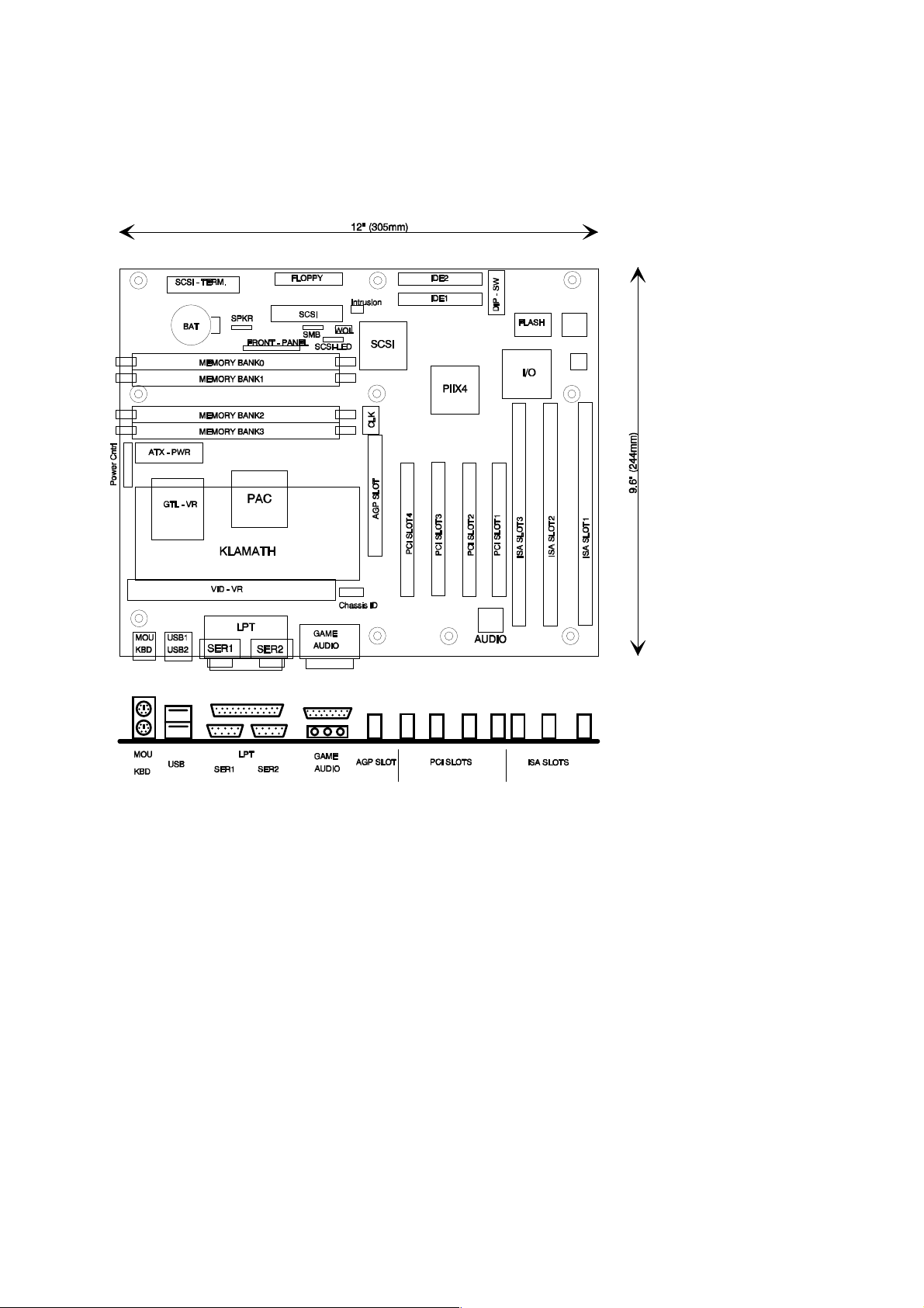
2 Mechanics
2.1 Layout
ATX 12'' x 9,6'' (305mm x 244mm)
CAUTION:
Computer mainboards and components contain very delicate IC chips. To protect them against
damage caused from electric static, you have to follow some precautions:
•
Unplug your computer when you work inside
•
Hold components by the edge, don't touch their leads
•
Use a grounded wrist strap
Place the mainboard and the components on a grounded antistatic pad whenever you work
outside the computer
2.2 Assembling Slot 1
Before inserting the CPU, you have to assembly the including retention module. Please be
carefully to avoid a damage of the mainboard.
A26361-D981-Z180-3-7619 Seite
2
Page 3
Additional Technical Manual D981
2.3 Connectors, DIP-Switch, Jumpers
2.3.1 Power-Supply Connector 1
Pin Signal
1 + 3.3V
2 + 3.3V
3 GND
4 + 5V
5 GND
6 + 5V
7 GND
8 POWER GOOD
9 + 5V SB
10 + 12V
11 + 3.3V
12 - 12V
13 GND
14 PS ON
15 GND
16 GND
17 GND
18 - 5V
19 + 5V
20 + 5V
Pin 11
Pin 1
2.3.2 Power ON Switch-Connector
Pin Signal
1 VCCHELP over 1K
2 Power-On Puls (high Asserted)
2.3.3 CPU-FAN Connector
Pin Signal
1 GND
2 FAN Power Supply
3 Sense
Pin 1
Pin 1
A26361-D981-Z180-3-7619 Seite
3
Page 4
Additional Technical Manual D981
2.3.4 SYS-FAN Connector
(optional)
Pin Signal
1 GND
2 + 12 V
3 Sense
2.3.5 Speaker Connector
Pin Signal
1 VCC
2 GND
3 Key
4 SPEAKER OUT
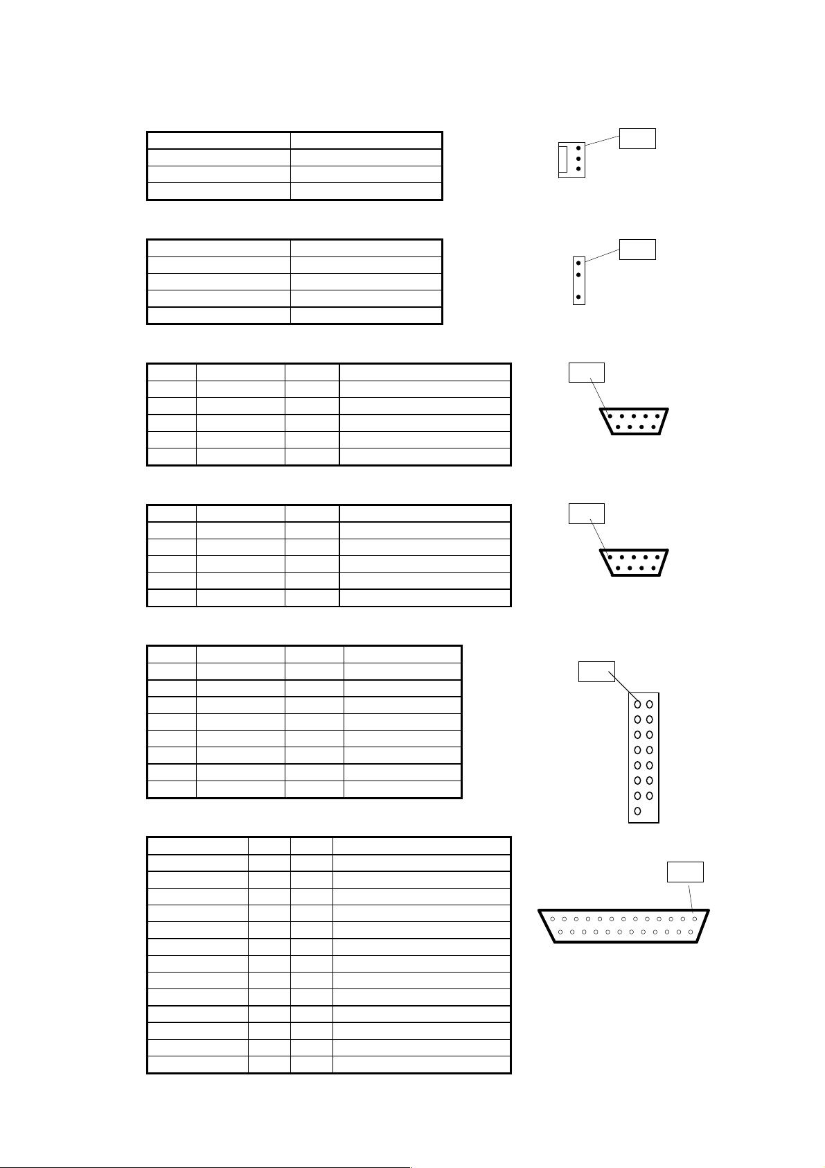
2.3.6 Serial Port 1 (V24)
Pin Signal Pin Signal
1 DCD 1 6 DSR 1
2 SIN 1 7 RTS 1
3 SOUT 1 8 CTS 1
4 DTR 1 9 RI 1 (Remote On)
5 GND
2.3.7 Serial Port 2 (V24)
Pin Signal Pin Signal
1 DCD 1 6 DSR 1
2 SIN 1 7 RTS 1
3 SOUT 1 8 CTS 1
4 DTR 1 9 RI 1
5 GND
Pin 1
Pin 1
Pin 1
Pin 1
2.3.8 Serial Port1 for Cardreader
Pin Signal Pin Signal
1 DCD 1 2 DSR 1
3 SIN 1 4 RTS 1
5 SOUT 1 6 CTS 1
7 DTR 1 8 PC_ON_Strobe
9 GND 10 VCCHELP
11 EXTSMI 12 VCC
13 RESETDRV 14 GND
15 GND 16 key
2.3.9 Parallel Port
Signal Pin Pin Signal
STROBE 1 14 AUTOFD
LPT DAT 0 2 15 ERROR
LPT DAT 1 3 16 INIT
LPT DAT 2 4 17 LPT SEL
LPT DAT 3 5 18 GND
LPT DAT 4 6 19 GND
LPT DAT 5 7 20 GND
LPT DAT 6 8 21 GND
LPT DAT 7 9 22 GND
ACK 10 23 GND
BUSY 11 24 GND
PEMTY 12 25 GND
SELECT 13
Pin 1
Pin 1
A26361-D981-Z180-3-7619 Seite
4
Page 5

Additional Technical Manual D981
2.3.10 Keyboard Port Connector
Pin Signal
1 KBD DAT
2 N.C.
3 GND
4 VCC
5 KBD CLK
6 Key ON/OFF
2.3.11 Mouse Port Connector
Pin Signal
1 MOUSE DAT
2 N. C.
3 GND
4 VCC
5 MOUSE CLK
6 N. C.
2.3.12 Floppy Connector
Pin Signal Pin Signal
1 GND 2 FDHDIN
3 GND 4 N.C.
5 Key 6 N.C.
7 GND 8 Index
9 GND 10 Motor Enable A
11 GND 12 Drive Select B
13 GND 14 Drive Select A
15 GND 16 Motor Enable B
17 GND 18 Step DIR
19 GND 20 Step Pulse
21 GND 22 Write Data
23 GND 24 Write Enable
25 GND 26 Track 0
27 GND 28 Write Protect
29 GND 30 Read Data
31 GND 32 Side 1 Select
Pin 1
Pin 3
Pin 1
Pin 2
Pin 3
Pin 1
Pin 2
Pin 2
2.3.13 Remote-On-Connector (=FAX On)
Pin Signal
1 GND
2 Remote On (Low active)
Pin 1
2.3.14 Voice Modem Connector
Pin Signal Pin Signal
1 Series-RC to PCSPK 2 N.C.
Pin 1
3 AGND 4 key
5 Micro to Modem 6 N.C.
2.3.15 CD IN Connector
Pin Signal
1 CD IN LEFT
2 GND
3 GND
4 CD IN RIGHT
A26361-D981-Z180-3-7619 Seite
Pin 1
5
Page 6

Additional Technical Manual D981
2.3.16 PCI-IDE Connector
Pin Signal Pin Signal
1 Reset Drive 2 GND
3 Data 7 4 Data 8
5 Data 6 6 Data 9
7 Data 5 8 Data 10
9 Data 4 10 Data 11
11 Data 3 12 Data 12
13 Data 2 14 Data 13
15 Data 1 16 Data 14
17 Data 0 18 Data 15
19 GND 20 Key
21 DRQ 22 GND
23 I/O Write 24 GND
25 I/O Read 26 GND
27 IORDY 28 N.C.
29 DACK 30 GND
31 IRQ 32 N.C.
33 ADR 1 34 N.C.
35 ADR 0 36 ADR 2
37 Chip Select 1 38 Chip Select 3
39 IDE-LED 40 GND
Pin 1
2.3.17 AUX Audio IN Connector (e. g. MPEG, TV-Cards)
Pin Signal
1 GND
2 MPEG Audio In LEFT
3 GND
4 MPEG Audio In RIGHT
2.3.18 Infrared Connector
Pin Signal
1 VCC
2 key
3 IRDA_RX
4 GND
5 IRDA_TX
2.3.19 Front Panel Connector 1
Pin Signal
1 Boot Lock
2 + Standby LED
3 Key
4 + Power LED
5 Key
6 - Standby/ Power LED
7 Keylock
8 GND
9 Key
10 + HD LED
11 HD LED
12 HD LED
Pin 1
Pin 1
Pin 1
A26361-D981-Z180-3-7619 Seite
6
Page 7

Additional Technical Manual D981
2.3.20 Front Panel Connector 2 (optional)
Pin Signal
1 Reset (Low asserted)
2 GND
3 Key
4 + Turbo LED
5 - Turbo LED
6 Key
7 Turbo Switch
8 GND
2.3.21 SCSI-LED Connector (symmetrical)
Pin Signal
1 N.C.
2 SCSI_LED
3 SCSI_LED
4 N.C.
Pin 1
2.3.22 SCSI - Connector
GND 1 35 SCSI_DB_L<12>
GND 2 36 SCSI_DB_L<13>
GND 3 37 SCSI_DB_L<14>
GND 4 38 SCSI_DB_L<15>
GND 5 39 SCSI_PAR1_L
GND 6 40 SCSI_DB_L<0>
GND 7 41 SCSI_DB_L<1>
GND 8 42 SCSI_DB_L<2>
GND 9 43 SCSI_DB_L<3>
GND 10 44 SCSI_DB_L<4>
GND 11 45 SCSI_DB_L<5>
GND 12 46 SCSI_DB_L<6>
GND 13 47 SCSI_DB_L<7>
GND 14 48 SCSI_PAR0_L
GND 15 49 GND
GND 16 50 GND
TERMPWR 17 51 TERMPWR
TERMPWR 18 52 TERMPWR
RESERVED 19 53 RESERVED
GND 20 54 GND
GND 21 55 SCSI_ATN_L
GND 22 56 GND
GND 23 57 SCSI_BSY_L
GND 24 58 SCSI_ACK_L
GND 25 59 SCSI_RST_L
GND 26 60 SCSI_MSG_L
GND 27 61 SCSI_SEL_L
GND 28 62 SCSI_CMD_L
GND 29 63 SCSI_REQ_L
GND 30 64 SCSI_IN_L
GND 31 65 SCSI_DB_L<8>
GND 32 66 SCSI_DB_L<9>
GND 33 67 SCSI_DB_L<10>
GND 34 68 SCSI_DB_L<11>
(optinal, only D981-A2x)
Pin-Nr.
Pin 1
Pin 35
Pin 68Pin 34
A26361-D981-Z180-3-7619 Seite
7
Page 8

Additional Technical Manual D981
2.3.23 1 or 2 USB Connector
Pin Signal
1 VCC
2 DATA_NEGATIVE
3 DATA_POSITIVE
4 GND
2.3.24 Wake up ON LAN Connector (optional)
Pin Signal
1 VCCHELP
2 GND
3 LAN_Wakeup
2.3.25 Intrusion Logic Connector (optional)
Pin Signal
1 GND
2 Chassis Open (low active)
3 Intrusion Logic Presence (low act.)
Pin 1
Pin 1
Pin 1
2.3.26 Power Control Connector (optional)
Pin Signal
1 Monitor-On
2 SV-Fan-Off-Req (low active)
3 SV-Fan-Full (low active)
4 SV-Fan-Puls
5 SMB-CLK
6 SMB-DATA
7 VCC-EEPROM
8 GND
Pin 1
A26361-D981-Z180-3-7619 Seite
8
Page 9
Additional Technical Manual D981
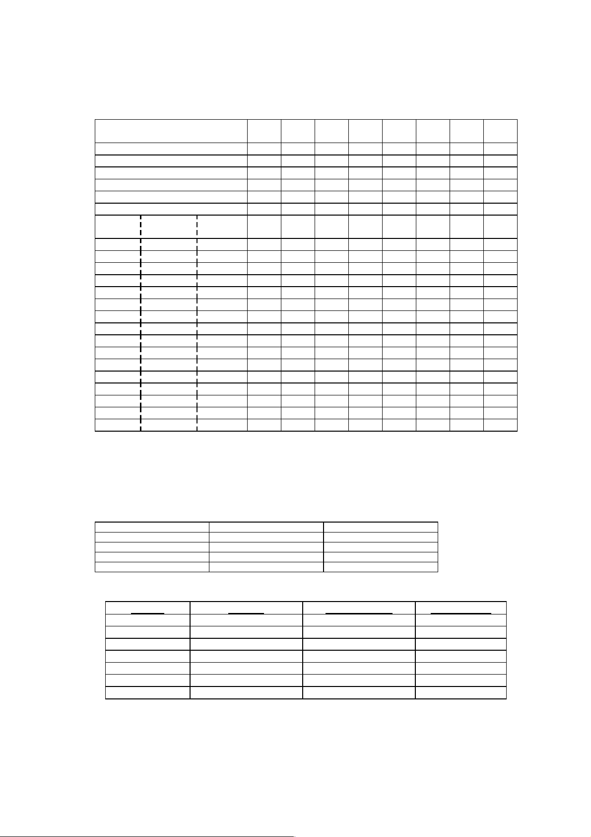
2.3.27 Configuration SWITCH-Block (DIP-Switch)
for Frequency selection, Flash write, Password clear, Recovery and Floppy write
Function: SW1
SKP
SW2
RCV
SW3
FWP
SW4
RES
SW5
CF1
SW6
CF2
SW7
CF3
SW8
CF4
Password Skip On x x x x x x x
Off Off x x x x x x x
Recovery BIOS x On x x x x x x
Off x Off x x x x x x
Floppy Write Protect x x On x x x x x
Off xxOffxxxxx
FRACT. RATIO Freq. at
66MHz
2/4 2 133 x x x x On On On On
2/5 2,5 166 x x x x On On On Off
2/6 3 200 x x x x On On Off On
2/7 3,5 233 x x x x On On Off Off
2/8 4 266 x x x x On Off On On
2/9 4,5 300 x x x x On Off On Off
2/10 5 333 x x x x On Off Off On
2/11 5,5 366 x x x x On Off Off Off
2/12 6 400 x x x x Off On On On
2/13 6,5 433 x x x x Off On On Off
2/14 7 466 x x x x Off On Off On
2/15 7,5 500 x x x x Off On Off Off
2/16 8 533 x x x x Off Off On On
2/3 1,5 100 x x x x Off Off On Off
Res - - x x x x Off Off Off On
2/4 2 133 x x x x Off Off Off Off
On = 1 = Close Off = 0 = Open x = don't care
For use of Pentium II Processors with host bus frequency of 66 MHz only !
Don't use Processor with 100 MHz host frequency !
2.3.28 PCI-SLOT Configuration And Placement
PCI-SLOT IDSEL Device Number
PCI-SLOT 1 ADR 25 0eh
PCI-SLOT 2 ADR 27 10h
PCI-SLOT 3 ADR 29 12h
PCI-SLOT 4 ADR 31 14h
2.4 Power Requirements (Power Supply)
Source Voltage Max. Variation Max. Current
SV + 5.1 V +/- 5 % 9,0 A
SV - 5 V +/- 5 % 0,0 A
SV + 12 V +/- 10 % 0,3 A
SV - 12 V +/- 10 % 0,1 A
on Board 1.8 - 3.5 V +/- 5 % 14,0 A
SV + 3,3 V +/- 5 % 2,0 A
SV + 5.0 V (aux)
−
ATX-compliant
−
for Wake up on LAN (WOL) you need a Power Supply with VCC Help = 500mA
*
10 mA
*
A26361-D981-Z180-3-7619 Seite
9
Page 10

Additional Technical Manual D981
g
g
g
g
g
g
g
3 Installing drivers and utilities; documentation
♦
Insert the "Drivers & Utilities" CD.
♦
When the
♦
Select the language in which you want to operate the user interface.
♦
Select
Here you will find the required drivers, utilities and the additional documentation
♦
For the following components, install the software offered to you in the HTML interface:
−
−
−
−
−
For more details please the according readme.txt files
DeskStart
Scenic Pro
Audio board (sound card) "Crystal"
Hard disk controller "PIIX4"
Software update
USB-Support
Adaptec-SCSI (only for D981-A1x with onboard SCSI-Controller)
4 Upgrades
4.1 Main Memory
Further information is given in the main technical manual.
For correct functionality of the mainboard D981 we recommend the usage of the following DIMMModules.
For upgrades of the following list, please ask your local dealer.
16MB DIMM SD-RAM, 2Mx64
Producer Part.-No
Samsun
window appears, select
and then select f.e.
Windows 95.
KMM366S203BTN-G0 and -G2
Explore the CD via HTML
.
32MB DIMM SD-RAM, 4Mx64
Producer Part.-No
NEC MC-454AD644F-A67
Siemens HYS64V4020GU-10
Samsun
32MB DIMM SD-RAM, 4Mx72
Producer Part.-No
Goldstar GMM2734233BLTG-10K
Hyundai HYM7V72A400TFG-10
Siemens HYS72V4020GU-10
Samsun
64MB DIMM SD-RAM, 8Mx64
Producer Part.-No
NEC MC-458CB644F-A10
Samsun
64MB DIMM SD-RAM, 8Mx72
Producer Part.-No
NEC MC459CA724F-A10
Samsun
128MB DIMM SD-RAM, 16Mx64
Producer Part.-No
NEC MC-4516CD644F-A10
Samsun
KMM366S403BTN-G0 and -G2
KMM374S4030BTN-G2
KMM366S823AT-G2
KMM374S823AT-G2
KMM366S1623AT-G2
128MB DIMM SD-RAM, 16Mx72
Producer Part.-No
NEC MC-4516CC724F-A10
Samsun
A26361-D981-Z180-3-7619 Seite
KMM374S1623AT-G2
10
Page 11

Additional Technical Manual D981
4.2 Wavetable-Upgrade
The mainboards D981-A and D981-B are prepared for a single chip wavetable-upgrade with
the Crystal CS9236.
To order please ask your local dealer.
A26361-D981-Z180-1-7619
Seite
11
 Loading...