

Page 1
MCU-AN-510014-E-10
FM3
32-BIT MICROCONTROLLER
MB9B500 Series
FSS MB9BF506R EV-BOARD
USER MANUAL
APPLICATION NOTE
For more information for the FM3 microcontroller, visit the web site at:
http://www.fujitsu.com/global/services/microelectronics/product/micom/roadmap/industrial/fm3/
FUJITSU SEMICONDUCTOR (SHANGHAI) LIMITED
Page 2

A
TM
RM and Cortex-M3 are the trademarks of ARM Limited in the EU and other countries.
ALL RIGHTS RESERVED
The contents of this document are subject to change without notice.
Customers are advised to consult with sales representatives before ordering.
The information, such as descriptions of function and application circuit examples, in this document are
presented solely for the purpose of reference to show examples of operations and uses of FUJITSU
SEMICONDUCTOR device; FUJITSU SEMICONDUCTOR does not warrant proper operation of the device with
respect to use based on such information. When you develop equipment incorporating the device based on such
information, you must assume any responsibility arising out of such use of the information. FUJITSU
SEMICONDUCTOR assumes no liability for any damages whatsoever arising out of the use of the information.
Any information in this document, including descriptions of function and schematic diagrams, shall not be
construed as license of the use or exercise of any intellectual property right, such as patent right or copyright, or
any other right of FUJITSU SEMICONDUCTOR or any third party or does FUJITSU SEMICONDUCTOR warrant
non-infringement of any third-party's intellectual property right or other right by using such information. FUJITSU
SEMICONDUCTOR assumes no liability for any infringement of the intellectual property rights or other rights of
third parties which would result from the use of information contained herein.
The products described in this document are designed, developed and manufactured as contemplated for
general use, including without limitation, ordinary industrial use, general office use, personal use, and household
use, but are not designed, developed and manufactured as contemplated (1) for use accompanying fatal risks or
dangers that, unless extremely high safety is secured, could have a serious effect to the public, and could lead
directly to death, personal injury, severe physical damage or other loss (i.e., nuclear reaction control in nuclear
facility, aircraft flight control, air traffic control, mass transport control, medical life support system, missile launch
control in weapon system), or (2) for use requiring extremely high reliability (i.e., submersible repeater and
artificial satellite).
Please note that FUJITSU SEMICONDUCTOR will not be liable against you and/or any third party for any claims
or damages arising in connection with above-mentioned uses of the products.
Please note that FUJITSU SEMICONDUCTOR will not be liable against you and/or any third party for any claims
or damages arising in connection with above-mentioned uses of the products.
Any semiconductor devices have an inherent chance of failure. You must protect against injury, damage or loss
from such failures by incorporating safety design measures into your facility and equipment such as redundancy,
fire protection, and prevention of over-current levels and other abnormal operating conditions.
Exportation/release of any products described in this document may require necessary procedures in accordance
with the regulations of the Foreign Exchange and Foreign Trade Control Law of Japan and/or US export control
laws.
The company names and brand names herein are the trademarks or registered trademarks of their respective
owners.
Copyright ©2010 FUJITSU SEMICONDUCTOR (SHANGHAI) LIMITED All rights reserved.
2
Page 3

Revision History
Date Version
2011-04-21 V1.0
3
Page 4

Table of Contents
REVISION HISTORY .................................................................................................3
1 INTRODUCTION.....................................................................................................5
1.1 Product Overview ......................................................................................................... 5
1.2 MB9B506 Series MCU ................................................................................................. 5
1.3 Board Features............................................................................................................. 6
2 HARDWARE SETTING...........................................................................................7
2.1 Main Features .............................................................................................................. 7
2.2 Jumpers Overview........................................................................................................ 8
2.3 Setting for UART On-Board Programming ................................................................... 8
2.4 Setting for USB On-Board Programming ..................................................................... 8
2.5 Setting for Debug Tool ................................................................................................. 9
3 FLASH ON-BOARD PROGRAMMING................................................................. 10
3.1 On-Board Programming via UART............................................................................. 10
3.2 On-Board Programming via USB ............................................................................... 11
4 SAMPLE CODE.................................................................................................... 13
4.1 UART.......................................................................................................................... 14
4.2 Nand Flash................................................................................................................. 16
4.3 RTC............................................................................................................................ 16
4.4 CAN............................................................................................................................ 17
4.5 USB Function ............................................................................................................. 18
4.6 USB Host....................................................................................................................19
4.7 LCD & AD & Key ........................................................................................................ 20
5 DEBUG TOOL AND IDE....................................................................................... 21
5.1 Debug with J-Link in IAR EWARM Workbench .......................................................... 22
5.2 Debug with U-Link ME in Keil uVision4 ...................................................................... 28
6 MATERIALS DOWNLOAD................................................................................... 34
4
Page 5
1 Introduction
1.1 Product Overview
FSS MB9BF506R EV-Board (PN: FSSDC-9B506-EVB) provides an economical and simple
means for study usage for MB9B506 series MCU. The board compatible with both 3.3 and
5V system contains abundant external resources (LCD, buttons, UART, Nand Flash, CAN…)
to demonstrate MCU periphery function.
It also provides standard 20 pin JTAG interface, which is both compatible with IAR and Keil
debug tool. In addition, it allows On-board programming with both USB and UART mode.
Figure 1-1: FSSDC-9B506-EVB Overview
1.2 MB9B506 Series MCU
MB9B506 series MCU is 32-bit general purpose MCU of FM3 family that features the
industry's leading-edge ARM Cortex-M3TM CPU and integrates Fujitsu's highly reliable and
high-speed secure embedded flash technology. This MCU can operate at up to 80MHz CPU
frequency and work at a wide voltage range (2.7V-5.5V), which can be both compatible with
3.3V and 5V system.
It includes a host of robust peripheral features, including motor control timers (MFT), base
timer (can be configured to PWM, PPG, Reload, PWC timer), ADCs, on-chip memory (up to
512K Flash, up to 64K SRAM) and a wide range of communication interfaces (USB, I2C,
SIO, LIN, CAN).
5
Page 6

The size of on-chip memory can be configured according to different part number and the
package is available in LQFP and BGA, shown in following table.
Product Flash SRAM Package
MB9BF500N/R 256kB 32kB
MB9BF504N/R 256kB 32kB
MB9BF505N/R 384kB 48kB
MB9BF506N/R 512kB 64kB
Table 1-1: Product List
N: LQFP-100
R: LQFP-120
N: LQFP-100/BGA-112
R: LQFP-120
N: LQFP-100/BGA-112
R: LQFP-120
N: LQFP-100/BGA-112
R: LQFP-120
1.3 Board Features
FSS MB9BF506R EV-Board includes following features:
Microcontroller MB9BF506R
2x UART-Transceiver (Female DB9 connector)
2x High-speed CAN-Transceiver (2 pin header)
1x USB-Host (Type-A connector)
1x USB-Device (Type-B connector)
32M x 8bit Nand Flash (K9F5608U0D)
2
High Stability I
C-Bus Interface RTC Module (RX-8025T)
Standard JTAG Interface on a 20 pin-header
128 x 64 matrix LCD
3x ‘User’ LED
4x ‘User’-button
1x ‘Reset’-button
1x potentiometer regulating input voltage to AD channel
All 120 pins routed to test pads
On-board 5V and 3V voltage regulators, ‘Power’-LED
Power supply via USB-Device, JTAG or external with 15V power connector
6
Page 7
2 Hardware Setting
)
2.1 Main Features
External Power
JTAG
Connector
CAN
TX0_2, RX0_2
DB9 Connector
15V
UART channel 0
DB9 Connector
UART channel 2
LED
LED2-LED4 (P1B-P19
LCD
Potentiome
ter
AD channel 7
USB Device
USB Host
Nand Flash
attached on external bus
CS7 area
RTC
attached on I
2
C channel 7
Key
“Reset”
RTC Battery
”2 pin header”
Key
“Left” (P40), “Right” (P43),
“Up” (P41), “Down” (P42)
7
Page 8
2.2 Jumpers Overview
Jumper Name Function Setting
J101-J103
J104
J-USBJ-USB+
J105 Mode setting
J106 Oscillator Selection
J107 P22 connection
J701 Voltage division
*1
*2
Power selection
Voltage selection
USB Host/Function
selection
Short J101: select external power
Short J102: select JTAG power
Short J103: select USB power
Short 1,2: 5V
Short 2,3: 3.3V
Short 1,2: USB Function
Short 2,3: USB Host
Short: Programming mode
Open: Normal mode
Short 1,2: when 4M oscillator is used
Short 2,3: when 48M oscillator is used
Short: connect P22 (UART_TX0) with MAX3232
Open: disconnect P22 (UART_TX0) with MAX3232
Short: when 5V power is used
Open: when 3.3V power is used
Table 2-1: Jumper List
Attention:
1) Never short J101-103 at the same time! When Keil U-Link ME is used, JTAG power
can not be used.
2) When Keil U-link is used, only 3.3V can be selected, never select 5V power!
2.3 Setting for UART On-Board Programming
Part Number Function Setting
UART-0
DB9 connector Connect with PC via RS232 cable
J106 Oscillator Selection Open
J105 Mode setting short
J107
P22 connection short
Table 2-2: Setting for UART On-Board Programming
2.4 Setting for USB On-Board Programming
Part Number Function Setting
USBFUNCTION USB function connector Connect with PC via USB cable
J-USBJ-USB+
Function/Host selection Short 1,2
J105 Mode setting Short
J106 Oscillator Selection Short 1,2
J107 P22 connection Open
J701 Voltage division
Table 2-3: Setting for USB On-Board Programming
Short: when 5V power is used
Open: when 3.3V power is used
8
Page 9
2.5 Setting for Debug Tool
Use IAR J-Link
Part Number Function Setting
20PIN-JTAG JTAG connctor Connect with J-Link
J101-J103
J104
Power selection
Voltage selection
J105 Mode setting Open
Use Keil U-Link ME
Part Number Function Setting
20PIN-JTAG JTAG connctor Connect with U-Link ME
J101-J103
J104
J105 Mode setting Open
Power selection
Voltage selection Short 2,3
Short J101: select external power
Short J102: select JTAG power
Short J103: select USB power
Short 1,2: 5V
Short 2,3: 3.3V
Table 2-4: Setting for J-Link
Short J101: select external power
Short J103: select USB power
Table 2-5: Setting for U-Link
9
Page 10
3 Flash On-Board Programming
There are two ways to program the on-chip Flash of MB9BF506 series MCU: UART OnBoard Programming and USB On-Board Programming.
3.1 On-Board Programming via UART
First check the hardware setting as introduced by section 2.3.
Install the UART programmer: PCWFM3_V01L01. (It can be downloaded on the web)
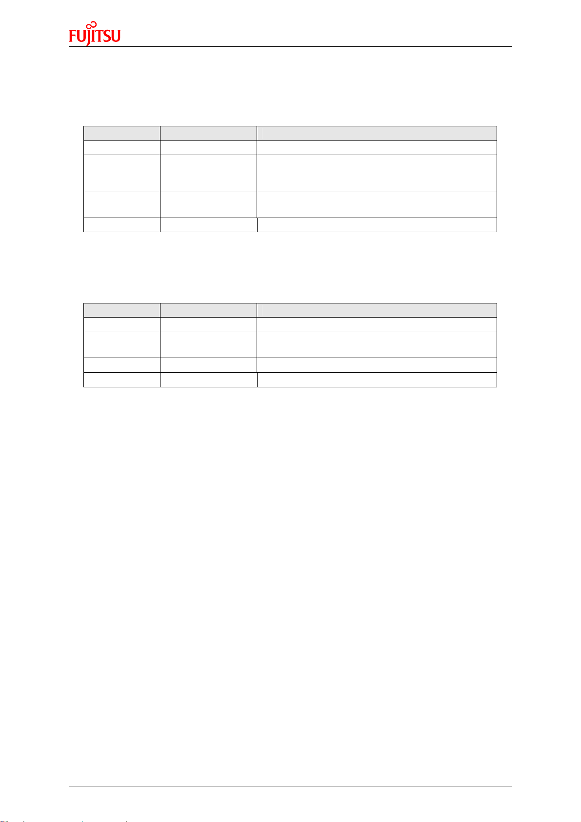
Open it, set the parameter as shown in following figure, and select Hex file.
Figure 3-1: UART Programmer Overview
Click Full Operation.
Figure 3-2: Press Reset Button
Press reset key in the board, and the programming will start.
Figure 3-3: Start Programming
10
Page 11
3.2 On-Board Programming via USB
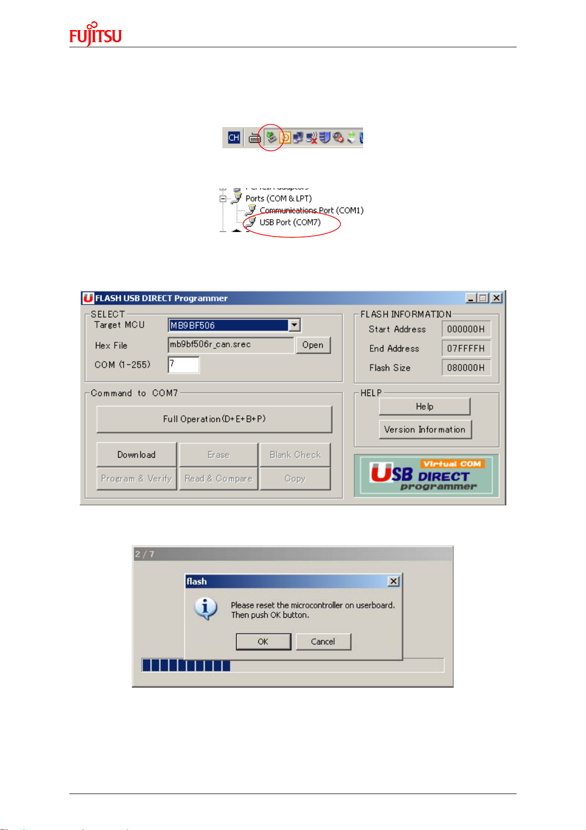
First check the hardware setting as introduced by section 2.4.
After connect with PC via USB cable, the EVB can be identified as a USB device.
Figure 3-4: USB Device Sign
Check the COM port for this USB port in the device manager.
Figure 3-5: COM Port in Device Manager
Install the USB programmer: USBDW_V01L03. (It can be downloaded on the web)
Open it, set the parameter as shown in following figure, and select Hex file.
Click Full Operation.
Figure 3-6: USB Programmer Overview
Figure 3-7: Press Reset Button
11
Page 12

Press reset key on the board. Programming will start.
Figure 3-8: Start Programming
12
Page 13

4 Sample Code
The sample codes for FSSDC-9B596-EV board are listed as following table.
Project Name Description
ext_bus_nandflash Use external bus to access Nand Flash
uart Use UART to communicate with PC
can
rtc Use IIC to access RTC module
usb_function_mose
usb_host_catch_mouse
lcd_ad_key Display ad value and key status on LCD
Notes:
1) It provides both IAR and Keil project for these sample code, IAR project is
developed in EWARM Embedded Workbench V6102, and Keil project is developed
in Keil uVision 4.20.
2) If user use other version to open these projects, compiling error may occur, in this
case, please check following setting.
IAR IDE
¾ MCU type
¾ Pre-included file
¾ ICF file
¾ Flash loader
Keil IDE
¾ MCU type
¾ Pre-included file
¾ ROM & RAM memory address
Implement CAN communication between 2
CAN nodes
Implement the USB mouse to demonstrate
USB function
Identify a USB mouse and print the mouse
position on debug window
13
Page 14

4.1 UART
Hardware Setting
Connect UART-2 with PC via RS232 cable
Flowchart
Figure 4-1: UART Sample Code Flowchart
Usage
1) Open a COM assistant software, make following setting, and open COM port
Figure 4-2: COM Assistant Setting
2) Open UART sample code and run it, user can watch a string on the COM assistant
window. Then send character to EV-board, the character can be received.
14
Page 15

Figure 4-3: Send UART Data From PC Side
15
Page 16

4.2 Nand Flash
Hardware Setting
None
Flowchart
Start
Initial external bus
(Use CS7 area,
8 bit data width)
Read Flash ID
Figure 4-4: Nand Flash Sample Code Flowchart
Erase page 11 of
block 0
Write data into
page 11 of block 0
Read data from
page 11 of block 0
Erase page 20 of
block 100
Write data into page
20 of block 100
Read data from page
20 of block 100
Usage
1) Open Nand Flash sample project, and start debug.
2) Use “step over” to debug, and watch local variable “flash_id”, “buf”.
4.3 RTC
Hardware Setting
End
It is an option that user can user external battery to supply power for RTC module
(RX8025-T) so that the date and time can be stored after system power shut down.
Flowchart
Start
Initial MFS channel 5
(set IIC mode)
Enable FOE signal
(FOUT output 32.768khz
wave after it is enabled)
Write 0 to second register Read to second register
Write 30 to minute register
Write 8 to hour register
Figure 4-5: RTC Sample Code Flowchart
Read to minute register
Read to hour register
16
Page 17

Usage
1) Open Nand Flash sample project, and start debug.
2) Use “step over” to debug, and watch local variable “sec”, “min”, “hour”.
4.4 CAN
Hardware Setting
Connect 2 EV-board with CAN interface, as following figure.
EV board 1
CAN 1
(Node A)
CAN 2
CAN 1
EV board 2
(Node B)
CAN 2
Figure 4-6: CAN Hardware Connection
Block Diagram
¾ Node A: use buffer 10 (ID = 0x12345678) to transfer and buffer 8 (ID = 0x08765432)
to receive
¾ Node B: use buffer 7 (ID = 0x12345678) to receive and buffer 10 (ID = 0x08765432)
to transfer.
Node A Node B
Buffer 10
(ID=0x12345678)
Buffer 7
(ID=0x12345678)
Buffer 8
(ID=0x08765432)
Buffer 10
(ID=0x08765432)
Figure 4-7: CAN Demo Block Diagram
Usage
1) Define “CAN_TX_RX” in the code, and compile, then program the code into Node A
2) Don’t define “CAN_TX_RX” in the code, and compile, then program the code into
Node B.
3) Connect Node A with Node B
When in real usage, user can program one node, and use the other node to debug.
17
Page 18

4.5 USB Function
Hardware Setting
¾ Check if 1,2 of J-USB- and J-USB+ short
¾ Check J701 (Short: 5V, Open: 3.3V)
¾ Connect with PC via USB cable
Flowchart
The following flowchart illuminates the procedure to implement a USB mouse, it is not a
certain flow of a function, but provides a clue to study and understand the sample code.
Start
Check ButtonInit(),
HIDInit()
Check
EXTI8_15_IRQHandler()
Device has been
connected with
Host
Button, USB core,
HID initialization
Check Ext INT7
occurred?
Initial Endpoint 0
Bus reset
Configure
Endpoint 0-5
Get Device, HID
description
Enable Endpoint 5
interrupt transfer
Use interrupt transfer to
communicate with host
USB_2_IRQHandler()
HidMouseSendReport()
USB_1_IRQHandler()
Figure 4-8: USB Function Sample Code Flowchart
Usage
1) Make the hardware setting.
2) Watch the mouse moving when pressing “Up”, “Down”, “Left”, “Right” buttons.
Check
Check
Check
18
Page 19

4.6 USB Host
Hardware Setting
¾ Check if 2,3 of J-USB- and J-USB+ short
¾ Connect with a USB mouse
Flowchart
The following flowchart illuminates the procedure to implement USB host function, which
can catch the position of a USB mouse, it is not a certain flow of a function, but provides
a clue to study and understand the sample code.
Start
SystemInit ( )
main ( )
minihost_init( )
Initialize system
clock
Initialize timer
Init USB host
Figure 4-9: USB Host Sample Code Flowchart
Enumeration
Mouse data
process
Display mouse
data
USB_Handler ( )
USBF_Handler ( )
get_mouse_data ( )
Main()
Usage
1) Make the hardware setting
2) Enable definition “Debug” in the code
3) Run the code.
4) Move the USB mouse, and watch the mouse position in the terminal IO window as
following figure. (Debug viewer window in Keil IDE)
Figure 4-10: USB Mouse Position Display
19
Page 20

4.7 LCD & AD & Key
Hardware Setting
None
Flowchart
(clock, key, lcd,
led, dual timer, ad)
Start
Initialization
Usage
Press key?
N
AD convert
Pre_AD_value-
Cur_AD_calue>threshold value
N
Count Time = 1s
N
Count time++
Y
Figure 4-11: LCD, key, AD Sample Code Flowchart
Set LCD update
flag
Y
Y
Count time = 0
N
LCD update flag = 1 ?
Clear LCD update
Set LCD update
flag
Y
flag
Display key
pressed in LCD
Display new AD
value on LCD
Clear window and
display logo in LCD
1) Run the code
2) Press key, and the key pressed can display on the LCD
3) Regulate the potentiometer to change the input voltage of channel 7, and this
voltage can be detected and displayed on LCD.
20
Page 21

5 Debug Tool and IDE
FSS MB9BF506R EV-Board supports both Keil U-Link-ME and IAR J-Link for debug shown
as following.
Figure 5-1: J-Link Overview
Figure 5-2: U-Link Overview
The U-Link-me should be used with Keil uVision 4 which can be downloaded freely from
following web.
https://www.keil.com/update/sw/RVMDK/4.20
The J-Link should be used with IAR Embedded Workbench which can be downloaded freely
from following web.
http://www.iar.com/website1/1.0.1.0/68/1/
21
Page 22

Tool bar
Project
list
5.1 Debug with J-Link in IAR EWARM Workbench
The sample code can be debugged in IAR EWARM Workbench with J-Link. The following
figure shows basic debug window.
Watch
window
Main
window
Log
window
Figure 5-3: IAR IDE Overview
Run an Existed Project
1) Open a project by clicking “File | Open | Workspace”
Figure 5-4: Open a Project
22
Page 23

2) Select a project (eww file)
3) Click “Project | Rebuild All”
Figure 5-5: Select a Project
Figure 5-6:Rebuild All
23
Page 24

4) Click “Download and Debug”
5) Use following tool bar to debug
Figure 5-7:Click Download and Debug
Figure 5-8: Debug Tool Bar
The sample codes support both Flash and RAM debug in IAR EWARM Workbench, if Flash
debug is used, the code is programmed into MB9BF506 Flash. If RAM debug is used, the
code only runs in RAM area, and after power off, the code will not be stored, but the RAM
debug will be faster than Flash debug.
Setting for Flash Debug
1) Check the configuration file path ($PROJ_DIR$\config\mb9bf506.icf) in Linker table.
Figure 5-9: ICF File for Flash Debug
24
Page 25

2) Don’t select “Use macro files” in “Debugger|Setup” table.
Figure 5-10: Macro File Disabled
3) Set Flash loader file path ($TOOLKIT_DIR$\config\flashloader\Fujitsu\MB9BF506.board)
in “Debug|Download” table.
Figure 5-11: Flash Load File Path
25
Page 26

Setting for RAM Debug
1) Check the configuration file path ($PROJ_DIR$\config\mb9bf506_ram.icf) in Linker
table.
Figure 5-12: ICF File for RAM Debug
2) Select “Use macro files” in “Debugger|Setup” table.
Figure 5-13: Macro File Enabled
26
Page 27

3) Don’t use Flash loader file.
Figure 5-14: Flash Loader File Disabled
If user need to program the hex file into Flash via UART or USB programmer, a hex file
need to be produced first.
How to Make a HEX File
1) Use Flash debug
2) Select “Generate additional output” in “Output Converter” table.
Figure 5-15: Hex File Genration in IAR IDE
3) User can find the generated file in path (../Debug/Exe)
27
Page 28

Tool bar
Project
list
Build
output
5.2 Debug with U-Link ME in Keil uVision4
The sample code can also be debugged in Keil μVersion4 with U-Link. The following figure
shows basic debug window.
Watch
window
Main
window
Figure 5-16: Keil IDE Overview
Run an Existed Project
1) Open a project by clicking “Project | Open Project…”
Figure 5-17: Open a Project
28
Page 29

2) Select a project (uvproj file)
3) Rebuild all
4) Start debug
Figure 5-18: Select a Project
Figure 5-19: Rebuild All Files
Figure 5-20: Start Debug
29
Page 30

5) Use following tool bar to debug
Figure 5-21: Debug Tool Bar
The sample codes support both Flash and RAM debug in Keil uVison 4, if Flash debug is
used, the code is programmed into MB9BF506 Flash. If RAM debug is used, the code only
runs in RAM area, and after power off, the code will not be stored, but the RAM debug will
be faster than Flash debug.
Setting for Flash Debug
1) Set ROM address in Flash area. (0x00000000-0x00080000)
Figure 5-22: ROM Address Setting for Flash Debug
30
Page 31

2) Don’t use initialization file.
Figure 5-23: Don’t use initialization File
3) Check “Update Target before Debugging” checkbox
Figure 5-24: Select Update Target Before Debugging
31
Page 32

Setting for RAM Debug
1) Set ROM address in Code SRAM area. (0x1fff8000-0x1fffffff)
Figure 5-25: Set RAM Address for RAM Debug
2) Set initialization file path. (..\Debug_RAM.ini)
Figure 5-26: Select Initialization File
32
Page 33

3) Don’t Check “Update Target before Debugging” checkbox
Figure 5-27: Select Update Target Before Debugging
If user need to program the hex file into Flash via UART or USB programmer, a hex file
need to be produced first.
How to Make a HEX File
1) Check “Create HEX File” checkbox (This file is Intel Format HEX)
Figure 5-28: HEX File Generation in Keil IDE
2) User can find the generated file in path “..\output\debug\”
33
Page 34

6 Materials Download
The following materials can be downloaded from below web.
http://www.fujitsu.com/cn/
Software
z FUJITSU Flash MCU Programmer
z FUJITSU Flash USB DIRECT Programmer
Document
z FSSDC-9B506-EVB User Manual
z FSSDC-9B506-EVB Schematic
z MB9B506 Series Datasheet
z MB9B506 Series Peripheral Manual
z MB9B506 Series Flash Programming Manual
Sample code
z uart
z iic_rtc
fss/events/contest/2010/index_download.html
z ext_bus_nandflash
z can
z usb_func_mouse
z usb_host_catch_mouse
z lcd_ad_key
IDE Study Material
z IAR IDE study material
z Keil IDE study material
34
 Loading...