

Page 1

FUJITSU SEMICONDUCTOR
MICROCONTROLLER MANUAL
HARDWARE MANUAL
CM25-10133-2E
F2MC-8L FAMILY
8-BIT MICROCONTROLLER
MB89990 Series
Page 2

Page 3

F2MC-8L FAMILY
8-BIT MICROCONTROLLER
MB89990 Series
HARDWARE MANUAL
FUJITSU LIMITED
Page 4

Page 5

PREFACE
Preface describes objectives and intended reader.
■
Objectives and Intended Reader
The MB89990 series of microcontrollers are mid-range of microcontroller. They are generalpurpose and high-speed products in the F
microcontrollers operating at low voltages. It has Timer, Remote-control transmission frequency
generator.
This manual covers the functions and operations of the MB89990 series of microcontrollers.
Refer to the
F2MC-8L Family Software Manual
2
MC-8L Family series of 8-bit single-chip
for instructions.
i
Page 6

1. The contents of this document are subject to change without notice. Customers are advised to consult
with FUJITSU sales representatives before ordering.
2. The information and circuit diagrams in this document are presented as examples of semiconductor
device applications, and are not intended to be incorporated in devices for actual use. Also, FUJITSU is
unable to assume responsibility for infringement of any patent rights or other rights of third parties
arising from the use of this information or circuit diagrams.
3. The contents of this document may not be reproduced or copied without the permission of FUJITSU
LIMITED.
4. FUJITSU semiconductor devices are intended for use in standard applications (computers, office
automation and other office equipments, industrial, communications, and measurement equipments,
personal or household devices, etc.).
CAUTION:
Customers considering the use of our products in special applications where failure or abnormal
operation may directly affect human lives or cause physical injury or property damage, or where
extremely high levels of reliability are demanded (such as aerospace systems, atomic energy controls,
sea floor repeaters, vehicle operating controls, medical devices for life support, etc.) are requested to
consult with FUJITSU sales representatives before such use. The company will not be responsible for
damages arising from such use witho ut prior approval.
5. Any sem iconductor device s have inherentl y a certain rate of failure. Y ou must protect against injury,
damage or loss from such failures by incorporating safety design measures into your facility and
equipment such as redundancy, fire protection, and prevention of over-current levels and other
abnormal operating conditions.
6. If any products described in this document represent goods or technologies subject to certain
restrictions on export under the Foreign Exchange and Foreign Trade Control Law of Japan, the prior
authorization by Japanese government should be required for export of those products from Japan.
©2000 FUJITSU LIMITED Printed in Japan
ii
Page 7

CONTENTS
CHAPTER 1 GENARAL ..................................................................................................... 1
1.1 Features ................................................................................................................................................ 2
1.2 Product Series ....................................................................................................................................... 3
1.3 Block Diagram ....................................................................................................................................... 5
1.4 Pin Assignment ...................................................................................................................................... 6
1.5 Pin Function Description ........................................................................................................................ 8
1.6 Handling Devices ................................................................................................................................. 12
CHAPTER 2 HARDWARE CONFIGRATION ................................................................... 13
2.1 CPU ..................................................................................................................................................... 14
2.2 Lock Control Block ............................................................................................................................... 19
2.3 Interrupt Controller ............................................................................................................................... 25
2.4 I/O Ports .............................................................................................................................................. 28
2.5 8/16-bit Timer (Timer 1 and Timer 2) ................................................................................................... 32
2.6 External Interrupt 1 .............................................................................................................................. 39
2.7 External Interrupt 2 (Wake Up) ............................................................................................................ 43
2.8 Remote-control Carrier Frequency Generator ..................................................................................... 45
2.9 Time-base Timer .................................................................................................................................. 48
2.10 Watchdog Timer Reset ........................................................................................................................ 51
CHAPTER 3 OPERATION ............................................................................................... 53
3.1 Clock Pulse Generator .................. ...... ....... ...... ....... ...... ....................................... ...... .......................... 54
3.2 Reset ................................................................................................................................................... 55
3.2.1 Reset Operation ............................................................................................................................. 56
3.2.2 Reset Source .................................................................................................................................. 57
3.3 Interrupt ............................................................................................................................................... 58
3.4 Low-power Consumption Modes ......................................................................................................... 60
3.5 Pin States for Sleep, Stop and Reset .................................................................................................. 61
CHAPTER 4 INSTRUCTIONS .......................................................................................... 63
4.1 Transfer Instructions ............................................................................................................................ 64
4.2 Operation Instruction ....................................... ....................................... ...... ....... ...... .......................... 66
4.3 Branch Instructions .............................................................................................................................. 68
4.4 Other Instructions ................................................................................................................................ 69
4.5 F2MC-8L Family Instruction Map ......................................................................................................... 70
CHAPTER 5 MASK OPTIONS ......................................................................................... 71
5.1 Mask Options ....................................................................................................................................... 72
APPENDIX ............................................................................................................................ 73
APPENDIX A I/O Map ................................................................................................................................ 74
APPENDIX B EPROM Setting for MB89P195 ............................................................................................ 76
iii
Page 8

FIGURES
Figure 1.4-1 Pin Assignment (FPT-28P-M02, DIP-28P-M03) ........................................................................ 6
Figure 1.4-2 Pin Assignment (MQP-48C-P01) ................................................................................................ 7
Figure 2.1-1 Memory Space of MB89990 Series of Microcontrollers ............................................................ 14
Figure 2.1-2 Arrangement of 16 bit Data in Memory ..................................................................................... 16
Figure 2.1-3 Arrangement of 16-bit Data during Execution of Instruction ..................................................... 16
Figure 2.1-4 Structure of Processor Status ...... ...... ....... ...... ....... ...... ....................................... ...... ................ 17
Figure 2.1-5 Rule for Translating Real Addresses at General-purpose Register Area ................................. 17
Figure 2.1-6 Register Bank Configuration ..................................................................................................... 18
Figure 2.3-1 Interrupt-processing Flowcha rt .......................................... ....... ...... ....... ...... ....... ...... ... ............. 27
Figure 2.4-1 Ports 00 to 07 and 30 to 37 ...................................................................................................... 30
Figure 2.4-2 Ports 40 to 45 ........................................................................................................................... 31
Figure 2.5-1 8/16-bit Timer Block Diagram ................................................................................................... 32
Figure 2.5-2 Description Diagram for Internal Clock Mode Operation .......................................................... 36
Figure 2.5-3 Flow Diagram for Timer Setting ................................................................................................ 36
Figure 2.5-4 Initialization of Equivalent Circuit .............................................................................................. 37
Figure 2.5-5 External Cock Mode Operation Description Diagram ............................................................... 37
Figure 2.5-6 Operation Diagram when Timer Stop Bit is Used ..................................................................... 38
Figure 3.1-1 Clock Pulse Generator .............................................................................................................. 54
Figure 3.2-1 Outline of Reset Operation ....................................................... ...... ....... ...... ....... ...................... 56
Figure 3.2-2 Reset Vector Structure ...................... ....... ...... ....... ...... ....................................... ...................... 56
Figure 3.3-1 Interrupt-processing Flowcha rt .......................................... ....... ...... ....... ...... ....... ...... ................ 58
iv
Page 9

TABLES
Table 1.2-1 Types and Functions of MB89990 Series of Microcontrollers ..................................................... 3
Table 1.5-1 Pin Function Description .............................................................................................................. 8
Table 1.5-2 Pins for External ROM ................................................................................................................. 9
Table 1.5-3 Input/Output Circuit Configurations ........................................................................................... 10
Table 2.1-1 Table of Reset and Interrupt Vectors ......................................................................................... 15
Table 2.2-1 Opeating State of Low-power Consumption Modes .................................................................. 21
Table 2.2-2 Selection of Oscillation Stabilization Time ................................................................................. 22
Table 2.2-3 Sources of Reset ....................................................................................................................... 24
Table 2.4-1 List of Port Functions ................................................................................................................. 28
Table 3.3-1 Interrupt Sources and Interrupt Vectors .................................................................................... 59
Table 3.4-1 Low-power Consumption Mode at Each Clock Mode ................................................................ 60
Table 3.5-1 Pin State of MB89990 ............................................................................................................... 61
Table 5.1-1 Mask Options ............................................................................................................................ 72
v
Page 10

vi
Page 11

CHAPTER 1 GENARAL
The MB89990 series contains microcontrollers with a full range of resources such as
timers, external interrupts, and remote-control function, as well as the F2MC-8L CPU
core for low-voltage and high-speed operation. This single-chip microcontroller is
suitable for small devices such as remote controllers incorporating compact packages.
1.1 Features
1.2 Product Series
1.3 Block Diagram
1.4 Pin Assignment
1.5 Pin Function Description
1.6 Handling Devices
1
Page 12

CHAPTER 1 GENARAL
1.1 Features
This section describes the features .
■
Features
• Minimum instruction execution time: 0.95 µs at 4.2 MHz (V
2
• CPU core common to F
• Instruction set su itable for controlle r: - M ult ipl y /su btr ac tio n i ns truction, - 16-bit oper ati on,
- Instruction test and branch instruction, - Bit operation instruction
•Two timers
• 8/16-bit timer/counter
• 20-bit time-base counter
• External interrupts
• Edge detection: 3 pins (edge direction enabled)
• Low-level interrupt: 8 pins (wake-up)
• Built-in remote-control carrier frequency generator
• Low-power consumption modes
• Stop mode: Almost no power consumption because oscillation stopped
• Sleep mode: 33% of normal power consumption because CPU stopped
• Package: SOP-28, SH-DIP-28 (mask ROM only)
MC-8L CPU
CC
= 3 V)
2
Page 13

1.2 Product Series
1.2 Product Series
This section describes the product series.
■
Product Series
Table 1.2-1 "Types and Functions of MB89990 Series of Microcontrollers"lists the types and
functions of the MB89990 series of microcontrollers.
Table 1.2-1 Types and Functions of MB89990 Series of Microcontr ollers
Model Name MB89997 MB89P195* MB89PV190*
Classification Mass-produced product (mask ROM
product)
ROM capacity 32 K × 8 bits
(internal ROM)
RAM capacity 128 × 8 bits 256 × 8 bits
CPU functions Number of basic instructions
Instruction bit length
Instruction length
Data bit length
Minimum instruction execution time
Interrupt processing time
Port I/O port (N-ch open drain)
I/O port (CMOS)
Total
Timer counter 2 channels 8-bit counter or 1 channel 16-bit counte
External-interrupt 1 3 independent channels (edge selection, interrupt vector, interrupt source flag)
Interrupt mode selectable from rising edge, falling edge, or both edges
For releasing Stop/Sleep modes (edge detection in Stop mode enabled)
136 instructions
8 bits
1 to 3 bytes
1, 8, 16 bits
0.95 µs/4.2 MHz
8.6 µs/4.2 MHz
6 pins
16 pins (13 used as resource pins)
22 pins
One-time product For evaluation
and development
16 K × 8 bits
(internal ROM,
write enable by
general-purpose
writer)
32 K × 8 bits
(external ROM)
External-interrupt 2
(Wake-up)
Remote-control
carrier frequency
Standby mode Sleep and Stop modes
Process CMOS
Package FPT-28P-M02, DIP-28P-M03 FPT-28P-M02 MQP-48C-P01
Operating voltage 2.2 to 6.0 V** 2.7V to 6.0 V
8 channels (Low-level interrupt enabled)
Pulse width and cycle are programmable
3
Page 14

CHAPTER 1 GENARAL
* The MB89P195 microtroller is the one-time product for the MB89190 series which can be also be used
for the MB89990 series.
* The MB89PV190 microtroller is the evaluation and development product for the MB89190 series which
can be also be used for the MB89990 series.
** Operating voltage varies with conditions such as frequency or others. See the data sheet for details.
4
Page 15
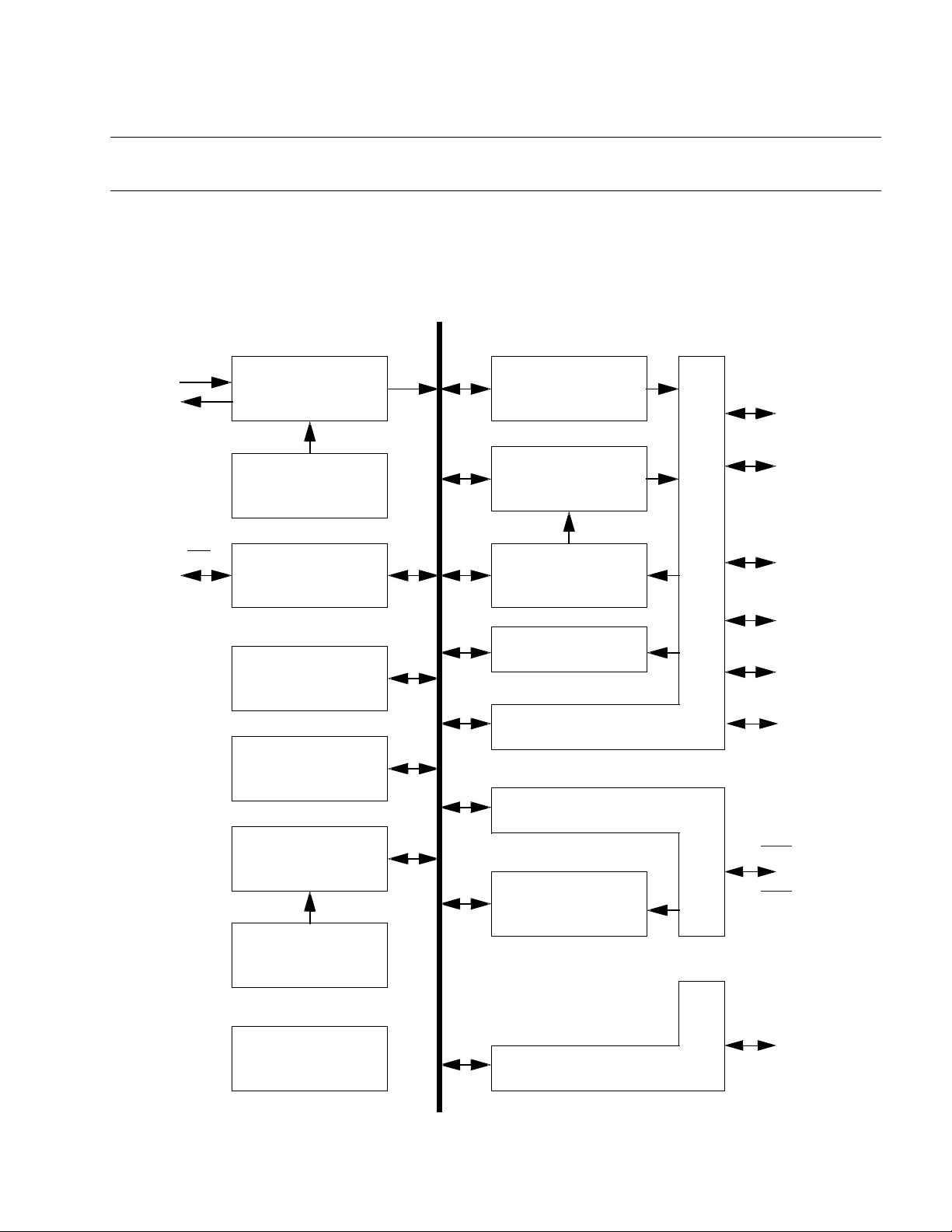
1.3 Block Diagram
This section describes the block diagram.
■
Block Diagram
Internal Bus
1.3 Block Diagram
X0
X1
RST
Main oscillator
circuit
Clock control
Reset circuit
(WDT)
Time-base timer
RAM
(128 x 8 bits)
Remote-control
carrier frequency
8-bit timer/counter
8-bit timer/counter
External Interrupt
CMOS I/O port
CMOS I/O port
P34/TO/INT10
P33 / EC
P30 ~ P32
Port 3
P35 / INT11
P36 / INT12
P37 / RCO
2
F
MC-8L
CPU
ROM
(32K x 8 bits)
TEST
Vcc, Vss
External Interrupt
(wake-up)
N-ch open drain I/O port
P00 / INT20 to
Port 0Port 4
P07 / INT27
P40 ~ P45
5
Page 16

CHAPTER 1 GENARAL
1.4 Pin Assignment
This section describes the pin assignment.
■
Pin Assignment
Figure 1.4-1 Pin Assignment (FPT-28P-M02, DIP-28P-M03)
P04/INT24
P05/INT25
P06/INT26
P07/INT27
TEST
RST
X0
X1
V
SS
P37/RCO
P36/INT12
P35/INT11
P34/TO/INT10
P33/EC
1
2
3
4
5
6
7
8
9
10
11
12
13
14
(TOP VIEW)
28
27
26
25
24
23
22
21
20
19
18
17
16
15
V
CC
P03/INT23
P02/INT22
P01/INT21
P00/INT20
P45
P44
P43
P42
P41
P40
P30
P31
P32
6
Page 17
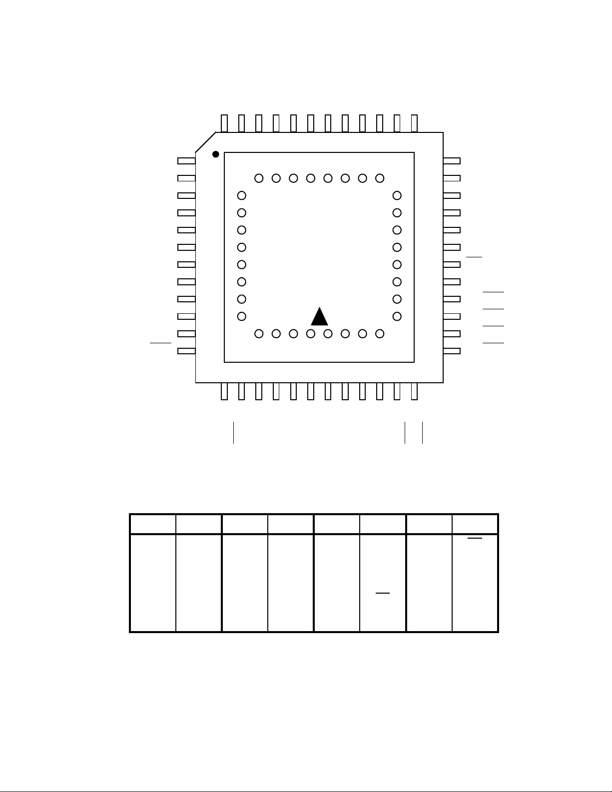
Figure 1.4-2 Pin Assignment (MQP-48C-P01)
P35/INT11
N.C.
N.C.
N.C.
N.C.
N.C.
Vss
N.C.
N.C.
N.C.
N.C.
48 47 46 45 44 43 42 41 40 39 38 37
1.4 Pin Assignment
N.C.
P34/TO/INT10
P33/EC
P32
P31
P30
P40
P41
P42
P43
P44
P45
P00/INT20
1
2
3
4
5
6
7
8
9
10
11
12
*
68 67 66 65 64 63 62 61
69
70
71
72
73
74
75
76
77 78 79 80 49 50 51 52
13 14 15 16 17 18 19 20 21 22 23 24
N.C.
N.C.
P10/INT21
(TOP VIEW)
N.C.
N.C.
N.C.
N.C.
Vcc
60
59
58
57
56
55
54
53
N.C.
N.C.
P02/INT22
P30/INT23
36
35
34
33
32
31
30
29
28
27
26
25
N.C.
N.C.
P36/INT12
P37/RCO
X1
X0
RST
TEST
P07/INT27
P06/INT26
P05/INT25
P04/INT24
* Pin assignment on package top (only for piggyback/evaluation product)
Pin No. Symbol Pin No. Symbol Pin No. Symbol Pin No. Symbol
49 V
PP 57 NC 65 04 73 OE
50A1258A2660574NC
51 A7 59 A1 67 06 75 A11
52 A6 60 A0 68 07 76 A9
53 A5 61 01 69 08 77 A8
54 A4 62 02 70 CE
78 A13
55 A3 63 03 71 A10 79 A14
56 NC 64 GND 72 NC 80 V
CC
7
Page 18
CHAPTER 1 GENARAL
1.5 Pin Function Description
This section describes the pin functions.
■
Pin Function Description
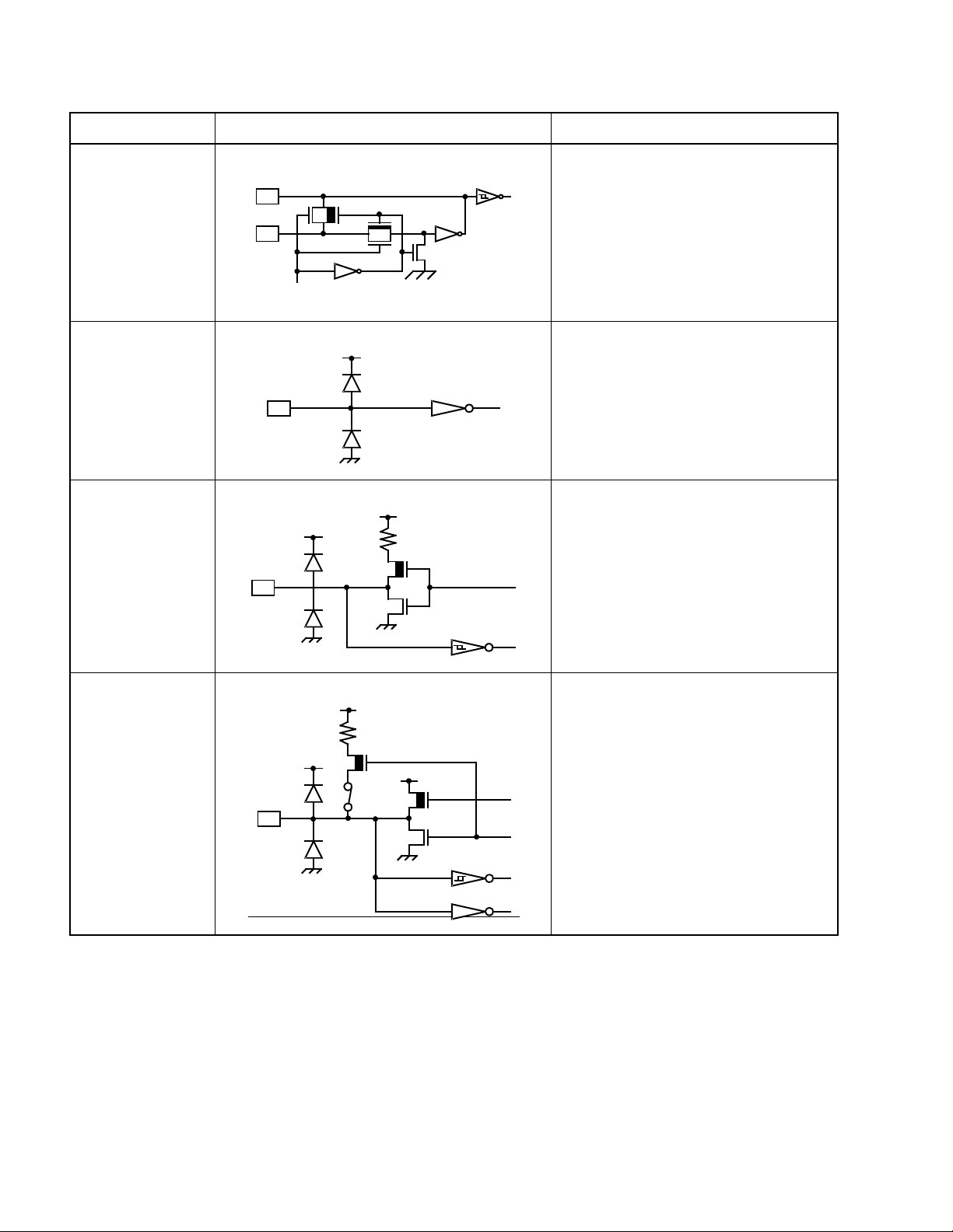
Table 1.5-1 "Pin Function Description" and Table 1.5-2 "Pins for External ROM" list the pin
function and Table 1.5-3 "Input/Output Circuit Configurations" shows the input/output circuit
configurations.
Table 1.5-1 Pin Function Description
Pin No. Pin Name Circuit type Function
7X0
8X1
5TEST B
RST
6
P00/INT20
24 to 27
1 to 4
17 P30 E
16 P31 E
15 P32 E
14 P33/EC D
to
P03/INT23
P04/INT24
to
P07/INT27
A
C
D
D
Clock oscillator pins
Test input pin
These pins are connected directly to V
Reset I/O pin
This pin consists of an N-ch open-drain output with a pull-up
resistor and hysteresis input. A Low level is output from this
pin by internal source. The internal circuit is initialized at
input of a Low level.
General-purpose I/O port
These ports also serve as external interrupt input pin.
The external interrupt input is hysteresis type.
General-purpose I/O port
These ports also serve as external interrupt input pin.
The external interrupt input is hysteresis type.
General-purpose I/O port
General-purpose I/O port
General-purpose I/O port
General-purpose I/O port
This port also serves as an external clock input pin for the 8bit timer/counter. The external clock input is hysteresis type
with a built-in noise filter.
SS
.
13 P34/T0/INT10 D
12 P35/INT11
11 P36/INT12
8
General-purpose I/O port
This port also serves as an overflow output pin and an
external interrupt input pin for the 8-bit timer/counter. The
external interrupt input is hysteresis type with a built-in noise
filter.
General-purpose I/O port
D
This port also serves as an external interrupt input pin. The
external interrupt input is hysteresis type with a built-in noise
filter.
Page 19
Table 1.5-1 Pin Function Description (Continued)
Pin No. Pin Name Circuit type Function
1.5 Pin Function Description
10 P37/RCO E
18 to 23 P40 to P45 F
28 V
9V
CC
SS
—
—
General-purpose I/O port
This port also serves as remote-control output pin.
N-ch open-drain type I/O port
Power pin
Power (GND) pin
Table 1.5-2 Pins for External ROM
Pin No. Pin Name Circuit type Functinon
49 V
79
78
50
75
69
76
77
51
52
53
54
55
58
59
60
PP
A14
A13
A12
A11
A10
A9
A8
A7
A6
A5
A4
A3
A2
A1
A0
Output
Output
High-level output pin
Address-output pins
61
62
63
65
66
67
68
69
01
02
03
04
05
06
07
08
70 CE
73 OE
80 V
64 V
CC
SS
Intput
Output
Output
Output
Output
Data-input pins
Chip-enable pin for ROM
A High level is output in the standby mode.
Output-enable pin for ROM
A Low level is always output.
Power pin for EPROM
Power (GND) pin
9
Page 20
CHAPTER 1 GENARAL
Table 1.5-3 Input/Output Circuit Configurations
Classification Circuit Remarks
A • Crystal oscillator
X1
• Feedback resistor: About 1 MΩ/5V
(1 to 5MHz)
X0
Standby control signal
B • CMOS input
C • Output pull-up resistor (P-ch):
About 50 kΩ (5 V)
R
• Hysteresi s inp u t
Pch
Nch
D • CMOS input/output
• Hysteresis input (resorce input)
R
Pch
Pch
Nch
• The pull-up resistor is available.
10
Page 21
1.5 Pin Function Description
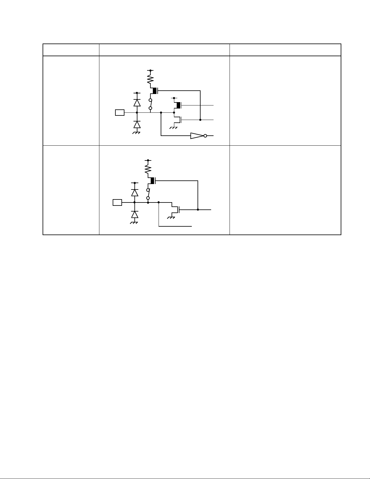
Table 1.5-3 Input/Output Circuit Configurations (Continued)
Classification Circuit Remarks
E • CMOS input/output
• The pull-up resistor is available.
R
Pch
Pch
Nch
F • N-ch open-drain output
• Analog input
R
Pch
• The pull-up resistor is available.
(MB89990 series only)
Nch
Analog input
11
Page 22

CHAPTER 1 GENARAL
1.6 Handling Devices
This section describes handling devices.
■
Handling Devices
(1) Preventing latch-up
Latch-up may occur if a voltage high er than V
or lower than VSS is applied to the input or
CC
output pins other than middle- and high-level-resistant pins, or if voltage exceeding the rated
value is applied between V
and VSS. When latch-up occurs, the supply current increases
CC
rapidly, sometimes r esulting in overheating and destruc tion. Therefore, no voltage exceeding
the maximum ratings should be used.
(2) Handling unused input pins
Leaving unused inp ut pin s open may cause a malfu nction. Therefore, t hese pin s shoul d be set
to pull-up or pull-down.
(3) Variations in supply voltage
Although the specif ied V
supply voltage op erating range is assured, a sud den change in the
CC
supply voltage within the specified range may cause a malfunction. Therefore, the voltage
supply to the IC should be kept as cons tant as possible. The V
supply frequency (50 to 60 Hz) should be less than 10% of the typical V
ripple (P-P value) at the
CC
value, or the
CC
coefficient of exces sive variati on should be less tha n 0.1 V/ms instantaneous change whe n the
power supply is switched.
(4) Precautions for external clocks
It takes some time for oscillation to stabilize after changing the mode from power-on reset
(option selection) and stop mode. Consequently, an external clock must be input.
(5) Recommended screening conditions
The OPTROM product should be screened by high-temperature aging before mounting.
12
Verify program
High-temperature aging (150°C, 48 H)
Read
Mount
The programming test can not be perform ed for all bi ts of the prep rogr ammed OPTROM product
due to its characteristics. Consequently, 100% programming yielding cannot be ensured.
Page 23

CHAPTER 2 HARDWARE CONFIGRATION
This chapter describes each block of the CPU hardware.
2.1 CPU
2.2 Clock Control Block
2.3 Interrupt Controller
2.4 I/O Ports
2.5 8/16-bit Timer (Timer 1 and Timer 2)
2.6 External Interrupt 1
2.7 External Interrupt 2 (Wake up)
2.8 Remote-control Carrier Frequency Generator
2.9 Time-base Timer
2.10 Watchdog Timer Reset
13
Page 24
CHAPTER 2 HARDWARE CONFIGRATION
2.1 CPU
• This section describes the memory space and register composing CPU hardware.
■
Memory Space
The MB89990 series of microc ontroller s have a memo ry area of 64K bytes . All I/O, data area s,
and program areas are located in this space. The I/O area is at the lowest address and the data
area is immediately above it. The data area may be divided into register, stack, and directaddress areas according to the applications. The program area is located near the highest
address and the tables of interrupt and reset vectors and vector-call instructions are at the
highest address. Figure 2.1-1 "Memory Space of MB89990 Series of Microc ontrollers" shows
the structure of the memory space for the MB89990 series of microcontrollers.
Figure 2.1-1 Memory Space of MB89990 Series of Microcontrollers
0000H
0080H
00C0H
0100H
0140H
8000H
FFFFH
MB89997
I/O
Vacant area
Register
Vacant area
Mask ROM
RAM
0000H
0080H
0100H
0180H
C000H
FFFFH
MB89P195
I/O
RAM
Register
Vacant area
Program PROM
(Mask ROM)
0000
0080H
0100H
0180H
8000H
FFFFH
MB89PV190
H
I/O
RAM
Register
Vacant area
External ROM
14
• I/O area
• This area is where various reso urce s such as contr ol and d ata reg ister s are loc ated. T he
memory map for the I/O area is given in APPENDIX A .
• RAM area
• This area is where the stati c RAM is lo cat ed. Ad dr es se s from
013F
for the MB89997) are also used as the general-purpose register area.
H
0100
H
to
017F
H
0100
(
• ROM area
• This area is whe re the in ter nal RO M is lo ca ted. Addresses fro m
FFC0
FFFF
to
H
H
to
H
are also
Page 25
used for the table o f reset and vector-c all instructions. T able 2.1-1 "Table of Reset and
Interrupt Vectors " shows the correspondence between each interrupt number or reset
and the table addresses to be referenced for the MB89990 series of microcontrollers.
Table 2.1-1 Table of Reset and Interrupt Vectors
Table address
Upper data Lower data
2.1 CPU
CALLV #0
CALLV #1
CALLV #2
CALLV #3
CALLV #4
CALLV #5
CALLV #6
CALLV #7
Interrupt #11
Interrupt #10
Interrupt #9
Interrupt #8
FFC0
FFC2
FFC4
FFC6
FFC8
FFCA
FFCC
FFCE
H
H
H
H
H
H
H
H
FFC1
FFC3
FFC5
FFC7
FFC9
FFCB
FFCD
FFCF
H
H
H
H
H
H
H
H
Table address
Upper data Lower data
FFE4
FFE6
FFE8
FFEA
H
H
H
H
FFE5
FFE7
FFE9
FFEB
H
H
H
H
Interrupt #7
Interrupt #6
Interrupt #5
Interrupt #4
Interrupt #3
Interrupt #2
Interrupt #1
Interrupt #0
Reset mode – – – –
Reset vector
Note:
FFFC
Set
is already reserved.
H
H
for
FFFD
in the Reset mode.
H
00
FFEC
FFFE
FFF0
FFF2
FFF4
FFF6
FFF8
FFFA
FFFE
H
H
H
H
H
H
H
H
H
FFED
FFEF
FFF1
FFF3
FFF5
FFF7
FFF9
FFFB
FFFD
FFFF
H
H
H
H
H
H
H
H
H
H
15
Page 26

CHAPTER 2 HARDWARE CONFIGRATION
■
Arrangement of 16-bit Data in Memory
When the MB89990 ser ies of microcontroller s handle 16-bit data, the data written at the lowe r
address is treated as the upper data and tha t written at th e next address is treated as the lower
data as shown in Figure 2.1-2 "Arrangement of 16 bit Data in Memory".
Figure 2.1-2 Arrangement of 16 bit Data in Memory
Before execution
1234H
A
Memory
ABCFH
ABCEH
ABCDH
ABCCH
MOVW ABCDH , A
After execution
1234H
A
Memory
34H
12H
ABCFH
ABCEH
ABCDH
ABCCH
This is the same as when 16 bits are specified by the operand during execution of an
instruction. Bits closer to the OP code are treated as the upper byte and those next to it are
treated as the lowe r byte. This is als o the same when the me mory a ddress or 1 6-bit i mmediate
data is specified by the operand.
Figure 2.1-3 Arrangement of 16-bit Data during Execution of Instruction
[Example]
MOV A, 5678
H ; Extended address
Assemble
XXXXH XX XX
Data saved in the stack by an interrupt is also treated in the same manner.
■
Internal Registers in CPU
The MB89990 serie s of microcontrollers have dedicated registers specifi ed applications in the
CPU and general-purpose registers in memory.
• Program counter (PC) 16-bit long register indicating location where instructions
• Accumulator (A) 16-bit long register where results of operations stored
• Temporary accumulator (T) 16-bit long register where the operations are performed
• Stack pointer (SP) 16-bit long register indicating stack area
XXXX
H 60 56 78 ; Extended address
H E4 12 34 ; 16-bit immediate data
XXXX
H XX
XXXX
stored
temporarily. The lower byte is used to execute 8-bit data
processing instructions.
between this register and the accumulator. The lower byte
is used to execute 8-bit data processing instructions.
16
Page 27
2.1 CPU
• Processor status (PS) 16-bit long register where register pointers and condition
codes stored
• Index register (IX) 16-bit long register for index modification
• Extra pointer (EP) 16-bit long register for memory addressing
16 bits
P C
A
T
IX
EP
SP
PS
Program counter
Accumulator
Temporary accumulator
Index register
Extra pointer
Stack pointer
Processor status
The 16 bits of the processor statu s (PS) can be divided into 8 upper bits for a register bank
pointer (RP) and 8 lower bits for a con dition code register (CCR ). (See Fig ure 2.1-4 "S tructure
of Processor Status".)
Figure 2.1-4 Structure of Processor Status
1514131211109876543210
PS
RP H I N Z V C
Vacant Vacant Vacant
IL1, 0
RP
CCR
The RP indicates the add ress of the cu rrent regi ster bank. T he contents of the RP and the re al
addresses are translated as shown in Figure 2.1-5 "Rule for Translating Real Addresses at
General-purpose Register Area" .
Figure 2.1-5 Rule for Translating Real Addresses at General-purpose Register Area
Lower bits of OP code
Source address
R P
'0' '0' '0' '0' '0' '0' '0' '1' R4 R3 R2 R1 R0 b2 b1 b0
A15 A14 A13 A12 A11 A10 A9 A8 A7 A6 A5 A4 A3 A2 A1 A0
The CCR has bits indicating the results of operations and transfer data contents, and bits
controlling the CPU operation when an interr upt oc curs .
- H-flag H-flag is set when a carry or a borrow out of bit 3 into bit 4 is generated
as a result of operations. It is cleared in other cases. This flag is used
for decimal-correction instructions.
17
Page 28
CHAPTER 2 HARDWARE CONFIGRATION
- I-flag An interrupt is enabled when this flag is 1 and is disabled when it is 0.
The I-flag is 0 at reset.
- IL1 and IL0 These bits indicate the level of the currently-enabled interrupt. The
Interrupt Processing executes interrupt processing only when an
interrupt with a value smaller than the value indicated by this bit is
requested.
IL1 IL0 Interrupt level High and low
0
0
1
1
- N-flag The N-flag is set when the most significant bit is 1 as a result of
operations. It is cleared when the MSB is 0.
- Z-flag Z-flag is set when the bit is 0 as a result of operations. It is cleared in
other cases.
0
1
0
1
1
2
3
High
Low = No interrupt
- V-flag V-flag is set when a twoís complement overflow occurs as a result of
operations. It is reset when an overflow does not occur.
- C-flag C-flag is set when a carry or a borrow out of bit 7 is generated as a
result of operations. It is cleared in other cases. When the shift
instruction is executed, the value of the C-flag is shifted out.
• General-purpose registers
General-purpose registers are 8-bit long registers for storing data.
The 8-bit long general- purpose registers are in the register ba nks in memory. One bank has
eight registers and up to 16 b anks are available for the MB89193 (8 banks for the MB89191).
The register bank pointer (RP) indicates the currently-used bank.
Figure 2.1-6 Register Bank Configuration
Address = 0100H + 8 (RP)
+
R0
R1
R2
R3
R4
R5
R6
R7
16 banks
18
Memory area
Page 29

2.2 Lock Control Block
• This block controls the standby operation and software reset.
■
Machine Clock Control Block Diagram
STP SLP SPL
2.2 Lock Control Block
Pin state
Stop
Sleep
Clock generator
From timebase timer
* f = oscillation
■
Register List
frequency
22/f*
12
/f
2
16
2
18
2
/f
/f
Selector
Stop release signal
Option
Address: 0008H STBC
8 bit
Clock control
R/W Stanby control register
CPU operation clock
Resource operation clock
19
Page 30

CHAPTER 2 HARDWARE CONFIGRATION
■
Description of Registers
The detail of each register is described below.
• Standby-control register (STBC)
Bit 7 Bit 6 Bit 5 Bit 4 Bit 3 Bit 2 Bit 1 Bit 0
Address: 0008
STP SLP SPL RST — — — —
H
(W) (W) (R/W) (W)
Intilial value
0001XXXX
B
[Bit 7] STP: Stop bit
This bit is used to specify switching CPU to the stop mode.
0 No operation
1 Stop mode
This bit is cleared at reset or stop cancellation.
0 is always read when this bit is read.
[Bit 6] SLP: Sleep bit
This bit is used to specify switching the CPU and resources to the sleep mode.
0 No operation
1 Sleep mode
This bit is cleared at reset, sleep or stop cancellation.
0 is always read when this bit is read.
[Bit 5] SPL: Pin state specifying bit
This bit is used to specify the external pin state in the stop mode.
0 Holds state and level immediately before stop mode
1 High impedance
This bit is cleared at resetting.
[Bit 4] RST: Software reset bit
This bit is used to specify the software reset.
0 Generates 4-cycle reset signal
1 No operation
1 is always read when this bit is read.
20
Page 31

■
Description of Operation
Main/sub clock block has normal and low-power consumption mode. The low-power
consumption mode are described below.
(1) Low-power consumption mode
This chip has three op eration m odes. T he slee p mode a nd stop mode i n the tabl e belo w reduce
the power consumption.
Table 2.2-1 Opeating State of Low-power Consumption Modes
Clock mode
of CPU
Clock pulse
Each operating clock pulse
(4 Mhz clock)
CPU
Time base
timer
resource
Each
2.2 Lock Control Block
Wake-up source
in each mode
RUN
Oscillates
Sleep
• The SLEEP mode stops only the operating clo ck pulse of the CPU. Other ope rations are
continued.
• The STOP mode stops the osci llation. Data c an be held with the lowest power consum ption
in this mode.
(a) SLEEP state
• Switching to Sleep State
• Writing 1 at the SLP bit (bit6) of the STBC register switches the mode to SLEEP state.
• The SLEEP state is the mode to stop clock pulse operating the CPU. Only the CPU
stops and the resources continue to operate.
• If an interrupt is requested when 1 is writte n at the SLP bit (bit 6), in struction execution
continues without switching to the SLEEP state.
• In the SLEEP state, the values of registers and RAM immediately before entering the
SLEEP state are held.
• Cancelling SLEEP state
2.0 MHz
Stops
2.0 MHz 2.0 MHz
Various interrupt
requests
• The SLEEP state is cancelled by inputting the reset signal and requesting an interrupt.
• When the reset sign al is input during the SLEEP state, the CPU is switched to t he reset
state and the SLEEP state is cancelled.
• When an interrupt l evel higher than 11 is reques ted from a resource during the SL EEP
state, the SLEEP state is cancelled.
• When the I flag and IL bit are enabled interrupt like an ordinary inte rrupt after cancelling,
the CPU executes th e interrupt processing. When they are disa bled, the CPU execute s
the interrupt proces sing from the instruction ne xt to the one before entering the SLEEP
state.
(b) STOP state
• Switching to STOP state
• Writing 1 at the STP bit (bit7) of the STBC register switches the mode to STOP state.
• In the STOP state, the clock oscillation, CPU, and all resources are stopped.
21
Page 32

CHAPTER 2 HARDWARE CONFIGRATION
• The input/output pins an d output pins during the STOP state can be controlled by the
SPL bit (bit5) of the STBC register so that they are held in the state immediately before
entering the STOP state, or so that they enter in the high-impedance state.
• If an interrupt is requ ested when 1 is written at the STP bi t (bit 7), instruction execution
continues without switching to the STOP state.
• In the STOP state, the values of registers and RAM immediately before entering the
STOP state are held.
• Cancelling STOP state
• The STOP state is cancelled either by inputting the reset signal or by requesting an
interrupt.
• When the reset signal is input during the STOP state, the CPU is switche d to the reset
state and the STOP state is cancelled.
• When an interrupt higher than level 11 is requested from the external interrupt circuit
during the STOP state, the STOP state is cancelled.
• When the I flag and IL bit a re enabled interrupt lik e an ordina ry interru pt after cancel ling,
the CPU executes the i nterrupt processing. When they are disabl ed, the CPU executes
the interrupt processing from the instruction next to the one before entering t he STOP
state.
• The oscillation st abilization ti me can be se lected by th e option from any of the four types
listed in Table 2.2-2 "Selection of Oscillation Stabilization Time".
• If the STOP state is cancelled by inpu tting the reset signal, the CPU is switched to the
oscillation stabiliz ation wait state. Therefore, the reset se quence is not executed unless
the oscillation s tabilizatio n time is elaps ed. The os cillation sta bilization time corresp onds
to the oscillation stabilization time of the main clock selected by the o ption. However,
when Power-on Reset is not s pecif ied by the mask option, the CP U is not s witch ed to the
oscillation stabilization wait state even if the STOP state is cancelled by inputting the
reset signal.
Table 2.2-2 Selection of Oscillation Stabilization Time
Ocillation stabilization time Ocillation stabilization time with 4 MHz source clock
18
2
/f* Approximate 65.5 ms
16
2
/f* Approximate 16.4 ms
12
2
/f* Approximate 1.2 ms
22/f* Approximate 0 ms
* f = source clock frequency
22
Page 33

(2) State transition diagram at low power consumption mode
SLEEP
Clock oscillate
(h)
STOP
Clock stop
(f)
(e)
2.2 Lock Control Block
(g)
(c)
Oscillation
stabilization waiting
(a) (b)
Power-on
(a) When power-on reset option selected
(b) When power-on reset option not selected
(c) After oscillation stabilized
(d) Set STP bit to 1.
(d)
Clock oscillate
RUN
(e) Set SLP bit to 1.
(f) External reset when power-on reset option not selected
(g) External reset or interrupt when power-on reset option selected
(h) External reset or interrupt
23
Page 34

CHAPTER 2 HARDWARE CONFIGRATION
■
Reset Control Section
Power-on reset
Watchdog timer reset
External reset
Software reset
• Reset
• There are four types of resets as shown in Table 2.2-3 "Sources of Reset".
Table 2.2-3 Sources of Reset
Reset name Description
Power-on reset Turns power on
Watchdog reset Overflows watchdog timer
External-pin reset Sets external-reset pin to Low
Software reset Writes 0 at RST bit (bit 4) of STBC
Reset control
Internal reset signal
When the power-on reset and reset dur ing the stop state are used, the oscillat ion stabilization
time is needed after the oscillator operates be cause the oscillator stops. The time-base timer
controls this stabilization time. Consequently, the operation does not start immediately even
after cancelling the reset.
However, if the mas k option w ith out Powe r-on Res et is sele cted, n o oscil lation stabi liza tion ti me
is required in any state after external pins have been released from the reset.
Note:
When resetting a product without the power-on reset function, set a longer time than the
optional oscillation stabilization time. Otherwise, the reset timing matches the AC
characteristics.
24
Page 35

2.3 Interrupt Controller
2.3 Interrupt Controller
• The interrupt controller for the F2MC-8L family is located between the CPU and each
resource. This controller receives interrupt requests from the resources, assigns
priority to them, and transfers the priority to the CPU. It also decides the priority of
same-level interrupts.
■
Block Diagram
CPU
F2MC-8L bus
Resource #1
Resource #2
Resource #n
■
Register List
2
Test reg-
ister
G L
G
•
G
Address decorder
Level
L
L
Level
Level
Level
deciding
block
G
G
•
G
Same level
priority order
deciding block
Interrupt vector generation
•
block
•
•
Interrupt controller consi sts o f interr upt-lev el re giste rs (IL R1, 2, an d 3) and in terrupt- test re giste r
(ITR).
8 bit
Address: 007CH
Address: 007DH
Address: 007EH
Address: 007FH
ILR1
ILR2
ILR3
ITR
W Interrupt level register #1
W Interrupt level register #2
W Interrupt level register #3
— Interrupt test register
25
Page 36

CHAPTER 2 HARDWARE CONFIGRATION
■
Description of Registers
The detail of each register is described below.
(1) Interrupt levei setting register (ILR1 to ILR3)
Bit 7 Bit 6 Bit 5 Bit 4 Bit 3 Bit 2 Bit 1 Bit 0
Address: 007C
Address: 007D
Address: 007E
The ILRX sets the interrupt level of each resource. The digits in the center of each bit
correspond to the interrupt numbers.
[Example]
Interrupt requests
from resources
L3X
H
H
H
L31 L30 L21 L20 L11 L10 L01 L00
L71 L70 L61 L60 L51 L50 L41 L40
LB1 LB0 LA1 LA0 L91 L90 L81 L80
Intilial value
11111111
MB89990 hardware manual
Interrupt control module
IR0
IR1
IR2
IR3
IRB
Interrupt
number
#0
#1
#2
#3
#11
Table address
Upper Lower
FFFA
FFFB
FFF8
FFF9
FFF6
FFF7
FFF4
FFF5
FFE4
FFE5
When an interrupt is requested from each resource, the interrupt controller transfers the
interrupt level based o n the value set at the 2 bits of th e ILRX corresponding to the interrupt to
the CPU.
A relation between two bits of the ILRX and the interrupt level required is shown below.
Lx1 Lx0 Required interrupt level
0X 1
10 2
1 1 3 (None)
(2) Interrupt test register (ITR)
Bit 7 Bit 6 Bit 5 Bit 4 Bit 3 Bit 2 Bit 1 Bit 0
Address: 007F
H
——————* *
The ITR used for testing. Do not access it.
26
Page 37

■
Description
2.3 Interrupt Controller
The functions of interrupt controllers are described below.
• Interrupt functions
• The MB89990 series of microcontrollers have 4 inputs for interrupt requests from each
resource. The inte rrupt level can be set by 2-bit registers corresponding to eac h input.
When an interrupt c an be requested from a re source, the interrupt contr oller receives it
and transfers the contents of the corresponding level register to the CPU. The interrupt to
the device is processed as follows:
(a) An interrupt source is generated inside each resource.
(b) If an interrupt is enabled, an interrupt request is output from each resource to the
interrupt controller by referring to the interrupt-enable bit inside each resource.
(c) After receiving this interrupt request, the interrupt controller determines the priority of
simultaneously-requested interrupts and then transfers the interrupt level for the
applicable interrupt to the CPU.
(d) The CPU compares the interrupt level requested from the interrupt controller with the
IL bit in the processor status register.
(e) As a result of the comparison, if the priority of the interrupt level is higher than that of
the current interrupt processing level, the contents of the I-flag in the same processor
status register are checked.
(f) As a result of the check in step (e), if the I-flag is enabled for an interrupt, the
contents of the IL bit are set to the required level. As soon as the currently-executing
instruction is terminated, the CPU performs the interrupt processing and transfers
control to the interrupt-processing routine.
(g) When an interrupt source generated in step (a) is cleared by software in the userís
interrupt processing routine, the CPU terminates the interrupt processing.
Figure 2.3-1 "Interrup t-processing Flowchart" outlines the inte rrupt operation for the MB89990
series of microcontrollers.
Figure 2.3-1 Interrupt-processing Flowchart
Internal bus
Register file
IPLA IR
PS I IL
Check Comparator
(f)
(e)
(d)
MB89990
(c)
Resource
(g)
Enable FF
Source FF
(a)
AND
Resource
Level
comparator
(b)
Interrupt controller
27
Page 38

CHAPTER 2 HARDWARE CONFIGRATION
2.4 I/O Ports
• he MB89990 series of microcontrollers have three parallel ports and 22 pins. P00 to
P07 and P30 to P37 se rve as 8-bit I/O ports, P40 to P45 serve as 6-bit I/O ports.
• Port0 and Port3 are also used as the I/O pin for the resource.
■
List of port functions
Table 2.4-1 List of Port Functions
Pin
name
P00 to
P07
P30 to
P37
P30 to
P37
■
Register List
Input
type
Output
type
Function bit7 bit6 bit5 bit4 bit3 bit2 bit1 bit0
Parallel
port 00 to
07
External
CMOS
CMOS
push-
pull
interrupt 2
Parallel
CMOS
Cmos
port 30 to
37
push-
Hysteresis
pull
Timer,
External
interrupt 1
CMOS
N-ch
open-
drain
Parallel
port 40 to
45
I/O port consists of the following registers.
P07 P06 P05 P04 P03 P02 P01 P00
INT27
INT26 INT25 INT24 INT23 INT22 INT21 INT20
P37 P36 P35 P34 P3 P32 P31 P30
ROC INT12 INT11
TO/
INT10
EC———
— — P45 P44 P43 P42 P41 P40
28
Address: 0000
Address: 0001H
Address: 000CH
Address: 000DH
Address: 000EH
8 bit
H
PDR0
DDR0
PDR3
DDR3
PDR4
R/W Port 00 to 07 data register
W Port 00 to 07 data direction register
R/W Port 30 to 37 data register
W Port 30 to 37 data direction register
R/W Port 40 to 47 data register
Initial value = XXXXXXXXB
Initial value = 00000000B
Initial value = XXXXXXXXB
Initial value = 00000000B
Initial value = XX111111B
Page 39

■
Description of Functions
The function of each port is described below.
(1) P00 to P07: CMOS type I/O ports
P30 to P37: CMOS type I/O ports
• Switching input and output
• This port has a data-dir ection register (DDR ) and a port-data regi ster (PDR) for each bit.
• Operation for output port (DDR = 1)
• The value written at the PDR is output to t he pin when the DDR is set to 1. When the
2.4 I/O Ports
(also used as resource input and output)
(also used as resource input and output)
Input and output c an be set inde pendently fo r each bit . The pin wit h the DDR set to 1 is
set to output, and the pin with the DDR set to 0 i s set to i nput. W hen the re source out put
bit is enabled, these ports are set to output irrespective of the DDR setting conditions.
PDR is read, usually, the value of the pin is r ead instead of the contents of the output
latch. However, when the Read Modify Write instruct ion is execute d, the cont ents of the
output latch are read irrespective of the DDR setting conditions. Therefore, the bitprocessing instruc tion can be used even if input and output are mi xed with each other.
When data is writt en to t he PDR, the wr it ten data i s hel d i n t he outp ut l atc h irr es pecti ve of
the DDR setting conditions.
• Operation for input port (DDR = 0)
• When used as the input port, the output impedance goes High. Therefore, when the PDR
is read, the value of the pin is read.
• Resource output operation
• When using as the reso urce output, setting is performed by t he resource output enable
bit. (See the description of each resource.) Since the reso urce output enable bit has
priority in switch ing input and output, even if the D DR is set to 0, any bit is set as the
resource output when output is ena bled at each resource. Even if the output from each
resource is enable d, the read parallel port is effective, so the resource ou tput value can
be checked.
• Resource input operation
• The pin value at a p ort with the resource input fu nction is always input for the resource
input (irrespective of the settin g of the DDR and resource). Set the DDR to input when
using an external signal for the resource input.
• State when reset
• When reset, the DDR and the outp ut enable bit for each resource a re initialized t o 0 and
the output impedance goes High at all bits. When reset, the PDR is not defined.
Therefore, set the value of the PDR before setting the DDR to output.
• State when stop
• With the SPL bit of the standby-control register set to 1, in the stop mode, the output
impedance goes High irrespective of the value of the DDR.
29
Page 40

CHAPTER 2 HARDWARE CONFIGRATION
Figure 2.4-1 Ports 00 to 07 and 30 to 37
To external interrupt
To resource input
External interrupt enable
Stop mode SPL = 1
Stop mode SPL = 1
Internal data bus
Resource
output
Resource
output EN
PDR
PDR read
PDR read
(when Read Modify Write instruction executed)
Output latch
PDR write
DDR
DDR write
Stop mode SPL = 1
(2) P40 to P45: N-ch open-drain-type output ports
(also used as analog input)
Pull-up resistor (option)
Pch
Pch
Pin
Nch
30
• Operation for output port
• The value written at the PDR is outpu t to the pin. When the PDR i s read in this port, the
contents of the output latch is always read instead of the value of the pin.
• State when reset
• The PDR is initialized to 1 at reset, so the output register is turned off at all bits.
• State in stop mode
• When the SPL bit of the standb y-control registe r is set to 1, in the stop mode , the output
impedance goes High irrespective of the value of the PDR.
Page 41

Internal data bus
Figure 2.4-2 Ports 40 to 45
PDR
PDR read
PDR read
(when Read Modify Write instruction is executed )
Output latch
PDR write
Stop mode (SPL = 1)
Stop
Pull-up resistor
(option)
Pch
Pin
Nch
2.4 I/O Ports
31
Page 42

CHAPTER 2 HARDWARE CONFIGRATION
2.5 8/16-bit Timer (Timer 1 and Timer 2)
• Three internal clock pulses and one external clock pulse can be selected.
• Operation in 8-bit 2-ch mode or 16-bit 1-ch mode can be selected.
• A square-wave output function is included.
■
Block Diagram
Figure 2.5-1 8/16-bit Timer Block Diagram
Internal data bus
T1STR T1STP T1CS0 T1CS1 T1OS0 T1OS1 T1IE T1IF
CLR
1/64
1/1024
Prescaler
CPU clock
P33/EC
CPU clock
Prescaler
1/64
1/1024
CLR
Square-wave
output initialization
pin control
R.S
1/4
MPX
1/4
MPX
CK
8-bit counter
CLR
Comparator
LOAD
Compare data latch
Data register
Data register
LOAD
Compare data latch
Comparator
CLR
8-bit counter
CK
CO
EQ
EQ
Q
TFF
IRQ3
P34/TO
/INT00
IRQ4
■
Register List
32
T2STR T2STP T2CS0 T2CS1 — — T2IE T2IF
8 bit
Address: 0018H
Address: 0019H
Address: 001AH
Address: 001BH
T2CR
T1CR
T2DR
T1DR
R/W Timer-2 control register
R/W Timer-1 control register
R/W Timer-2 data register
R/W Timer-1 data register
Page 43

■
Description of Register Details
The detail of each register is described below.
(1) Timer 1 control register (T1CR)
2.5 8/16-bit Timer (Timer 1 and Timer 2)
Bit 7 Bit 6 Bit 5 Bit 4 Bit 3 Bit 2 Bit 1 Bit 0
Address: 0019
T1IF T1IE T1OS1 T1OS0 T1CS1 T1CS0 T1STP T1STR
H
(R/W) (R/W) (R/W) (R/W) (R/W) (R/W) (R/W) (R/W)
Intilial value
X00000X0
B
[Bit 7] T1IF: Interrupt request flag
(When write)
0 Interrupt request flag clearing
1 No operation
(When read)
0 No interrupt request
1 Interval interrupt request
1 is always read when the Read Modify Write instruction is executed.
[Bit 6] T1IE: Interrupt-enable bit
0 Interrupt disabled
1 Interrupt enabled
[Bit 5 and 4] T1OS1, T1OS0: Square-wave output control bit
T1OS1 T1OS0
0 0 Makes square-wave output port (P43) general-purpose port
0 1 Holds data setting square-wave output to Low level
1 0 Holds data setting square-wave output to High level
1 1 Sets square-wave output to held value
When the T1STR bit is 0, the square-wave output is set to the set value.
33
Page 44
CHAPTER 2 HARDWARE CONFIGRATION
[Bit 3 and 2] T1CS1, T1CS0: Clock source select bit
T1CS1 T1CS0
00 2.0 [
0 1 32.0 [µs]
1 0 512 [µs]
Clock cycle time
selected at 4 MHz
µ
s]
Clock cycle time
×
2 instruction cycle
×
32 instruction cycle
×
512 instruction cycle
1 1 External clock
Note:
When using Timer 1 in the 8- bit mode, the clock source sel ect io n bit s (T 1CS1 and T1CS0) of
the Timer 2 control register (T2CR) must be set to other than the 16-bit mode.
[Bit 1] T1STP: Timer-stop bit
0 Counting continued without clearing counter
1 Counting suspended
[Bit 0] T1STR: Timer-start bit)
0 Terminates operation
1 Clears counter and starts operation
(2) Timer 2 control register (T2CR)
Bit 7 Bit 6 Bit 5 Bit 4 Bit 3 Bit 2 Bit 1 Bit 0
Address: 0018
T21F T21E — — T2CS1 T2CS0 T2STP T2STR
H
(R/W) (R/W) (R/W) (R/W) (R/W) (R/W) (R/W) (R/W)
[Bit 7] T2IF: Interrupt request flag bit
(When write)
0 Interrupt request flag cleari ng
1 No operation
(When read)
0 No interrupt request
Intilial value
X00000X0
B
34
1 Interval interrupt request
1 is always read when the Read Modify Write instruction is executed.
Page 45

[Bit 6] T2IE: Interrupt-enable bit
0 Interrupt disabled
1 Interrupt enabled
[Bit 3 and 2]: T2CS1, T2CS0: Clock source select bit
2.5 8/16-bit Timer (Timer 1 and Timer 2)
T2CS1 T2CS0
00 2.0 [
Clock cycle time
selected at 4 MHz
µ
s]
0 1 32.0 [µs]
1 0 512 [µs]
1 1 16 bit mode
[Bit 1] T2STP: Timer stop bit
0 Operation continued without clearing counter
1 Count operation suspended
[Bit 0] T2STR: Timer start bit
0 Operation stopped
1 Operation started after clearing counter
(3) Timer 1 and 2 data registers (T1DR and T2DR)
Clock cycle time
×
2 instruction cycle
×
32 instruction cycle
×
512 instruction cycle
Bit 7 Bit 6 Bit 5 Bit 4 Bit 3 Bit 2 Bit 1 Bit 0
Address: 001B
Address: 001A
H
H
(R/W) (R/W) (R/W) (R/W) (R/W) (R/W) (R/W) (R/W)
Intilial value
XXXXXXXX
B
Write data is the set interval times and read data is the counted times.
35
Page 46

CHAPTER 2 HARDWARE CONFIGRATION
■
Description of Operation
(1) 8-bit internal clock mode
In the 8-bit internal clock mode, thr ee internal clock inputs can be selected by setti ng the clock
source select bits (T 1CS1 and T1 CS0, T2CS1 and T2CS0) of the ti mer control registers (T1CR
and T2CR). The timer data registers (T1DR and T2DR) serve as interval time setting registers.
To start the timer, set the inte rval time as the timer data registers, write 1 at the timer start bits
(T1STR and T2STR) of the timer control registers to clear the counter to 00
values of the timer data registers into the compare latch. Then, counting starts.
When the values of the counter agree wi th thos e of the time r data re gis ters , the in ter val in ter r upt
request flags (T1IF and T2IF) are set to 1. At this time, the counter is cleared to 00
of the timer data re giste rs a re r el oad ed into th e com par e lat ch , an d c ou nti ng is c ontinue d. If the
interrupt enable bits (T1IE and T2IE) are set to 1, an interrupt request is output to the CPU.
Assuming the se t value of the timer data register is n a nd the selected clock is φ, the interval
time (T) can be calculated as follows.
T = φ × (n + 1) [µs]
Figure 2.5-2 Description Diagram for Internal Clock Mode Operation
Matched Matched Matched
Counter clear
Set data value
, and load the
H
, the values
H
Compare latch
Count value
0000H
T1STR
T1IF
TO
T1IF = 0 (W) T1IF = 0 (W) T1IF = 0 (W)
Figure 2.5-3 Flow Diagram for Timer Setting
Operation mode specification
Interval time setting
T1STR = 1, T1IF = 0, T1IE = 1
Timer start
Main program
T1IF = 1
Interrupt processing
T1IF = 0 (W)
36
Page 47

2.5 8/16-bit Timer (Timer 1 and Timer 2)
(2) Initializing square-wave output
The square-wave output can be set to any value only when the timer stops (T1STR = 0 and
T2STR = 0).
To set, proceed as follows:
(a) Write the set values (01 and 10) at the initialize bits (T1OS1 and T1OS0, T2OS1 and
T2OS2, respectively) of the square wave output.
(b) Write 11 at the same bits. This initializes the square wave output to the set value. If
the T1STR bit is set to 0, the square wave output of the pin is set to the set value
during this write cycle.
Figure 2.5-4 Initialization of Equivalent Circuit
T1STR, T2STR
Level latch
D5
Q
D
QX
D
Q
QX
SET
(3) 8-bit external clock mode
In the 8-bit external clock mod e, the external clock input can be selected by setting the clock
source select bits (T1CS1 and T1CS0) of the timer 1 control register (T1CR).
To start the timer, write 1 at the ti mer start bit (T1S TR) of the T1 CR to clear the co unter. Then,
counting starts.
When the value of the cou nter agrees with that of the timer data regist er setting, the interval
interrupt request fla g bit (T1IF) is set to 1. At this time, i f an interrup t is enabled ( T1IE = 1), an
interrupt request is output to the CPU.
ECK
Counter clear
TSTR = 1
Count value
T1IF
T1DR
D4
Write
D
Q
QX
Q
D
QX
RST
Figure 2.5-5 External Cock Mode Operation Description Diagram
Undefined 00 00H 01H 02H 00H 01H
FEH FFH
FFHFFH
T1IF = 0 (W)
37
Page 48

CHAPTER 2 HARDWARE CONFIGRATION
(4) Precautions for use of timer stop bit
Since an input c lock pu ls e is fi xed to Hig h l ev el wh en the ti mer i s s topp ed by th e tim er s tar t bit s,
the count value differs depending on the state of the input clock pulse.
When writing 00 at the timer stop and timer start bits simultaneously after stopping the timer
with the timer stop bit, the count ma y be incr emented by 1. Theref ore, if the tim er is stop ped by
the timer stop bit, rea d the counter and then write 00 at the timer start bits (See Figure 2.5-6
"Operation Diagram when Timer Stop Bit is Used".).
Figure 2.5-6 Operation Diagram when Timer Stop Bit is Used
When input clock is High When input clock is Low
CK
CK'
TSTP
TSTR
TSTR'
Count value
(5) 16-bit mode
In the 16-bit mode, each bit of the timer control registers is as shown below.
Bit 7 Bit 6 Bit 5 Bit 4 Bit 3 Bit 2 Bit 1 Bit 0
Address: 0019
Address: 0018
T1IF T1IE T1OS1 T1OS0 T1CS1 T1CS0 T1STP T1STR
H
T2IF T2IF — — TECS1 TECS0 T2STP T2STR
H
No operation Set to 00 Set to 11 No operation
In the 16-bit mode, write 11 a t the T 2CS 1 a nd T2 CS0 bi ts of th e T 2CR and set 00 at the T2OS1
and T2OS0 bits.
When in the 16-b it mode, the ti mer is controll ed by the T1C R. The timer d ata registers T2DR
and T1DR use the upper and lower bytes, respectively.
The clock source is selec ted by the T1CS1 and T1CS0 bits of the T1CR. To start the ti mer,
write 1 at the T1STR bit of the T1CR to clear the counter.
If the value of th e counter a grees with that of th e timer data register , the T1IF b it is set to 1. At
this time, an interrupt request is output to the CPU if the T1IE bit is 1.
Note:
38
To read the valu e of the counter in the 16-bi t mode, always read the value twice to check
that it is valid, and then use the data.
See the 8-bit operation diagram for 16-bit mode operation.
Page 49

2.6 External Interrupt 1
2.6 External Interrupt 1
• The edges of three external-interrupt sources (INT10 to INT12) can be detected to
set the corresponding flag.
• An interrupt can be generated at the same time the flag is set.
• The three interrupts can release the STOP or SLEEP mode.
■
Block diagram
P35/INT11
MUX MUX
P34/TO/
INT 10
■
Registers
EIR1 SL11 SL10 EIE1 EIR0 SL01 SL00 EIE0 EIC1
IRQ0
IRQ1
P36/INT12
MUX
EIR2 SL21 SL20 EIE2 EIC2
IRQ2
Address: 0023H
Address: 0024H
8 bit
EIC1
EIC2
R/W External-interrupt control register 1
R/W External-interrupt control register 2
39
Page 50

CHAPTER 2 HARDWARE CONFIGRATION
■
Description of Registers
(1) External-interrupt control register 1 (EIC1)
The EIC1 controls interrupts by the INT10 and INT11 pins.
Bit 7 Bit 6 Bit 5 Bit 4 Bit 3 Bit 2 Bit 1 Bit 0
Address: 0023
EIR1 SL11 SL10 EIE1 EIR0 SL01 SL00 EIE0
H
(R/W) (R/W) (R/W) (R/W) (R/W) (R/W) (R/W) (R/W)
Intilial value
00000000
B
[Bit 7] EIR1: External-interrupt request flag
When the edge specified by the SL11 and SL10 bits is inp ut to the INT11 pin, bit 7 is set to 1.
When the EIE1 bit is 1, an interrupt request (IRQ1) is output if this bit is set.
The meaning of each bit to be read is as follows:
0 Specified edge not input to INT11 pin
1 Specified edge input to INT11 pin (IRQ1 is output.)
1 is always read when the Read Modify Write instruction is read.
The meaning of each bit to be written is as follows:
0 This bit is cleared.
1 This bit does not change nor affect other bits.
[Bit 6 and 5] SL11, SL10: Edge-polarity select bit
This bit is used to control the input edge polarity of the INT11 pin.
SL11 SL10
0 0 No edge detection
0 1 Rising edge
1 0 Falling edge
1 1 Both-edge mode
[Bit 4] EIE1: Interrupt-enable bit
This bit is used to enable an external-interrupt request by the INT11 pin.
0 Interrupt request disab led
1 Interrupt request enabled by EIR1 setting
40
Page 51

2.6 External Interrupt 1
[Bit 3] EIR0: External-interrupt request flag
When the edge specified by the SL01 and SL00 bits is inp ut to the INT10 pin, bit 3 is set to 1.
When the EIE0 is 1, an interrupt request (IRQ0) is output if this bit is set.
The meaning of each bit to be read is as follows:
0 Specified edge not input to INT10 pin
1 Specified edge input to INT10 pin (IRQ0 is output.)
1 is always read when the Read Modify Write instruction is read.
The meaning of each bit to be written is as follows:
0 This bit is cleared.
1 This bit does not change nor affect other bits.
[Bit 2 and 1] SL01, SL00: Edge-polarity select bit
This bit is used to control the input edge polarity of the INT10 pin.
SL01 SL00
0 0 No edge detection
0 1 Rising edge
1 0 Falling edge
1 1 Both-edge mode
[Bit 0] EIE0: Interrupt-enable bit
Bit 0 is used to enable an external-interrupt request by the INT10 pin.
0 Interrupt request disabled
1 Interrupt request enabled by EIR0 setting
(2) External-interrupt control register 2 (EIC2)
The EIC2 controls an interrupt by the INT12 pins.
Bit 7 Bit 6 Bit 5 Bit 4 Bit 3 Bit 2 Bit 1 Bit 0
Address: 0024
H
————EIR2SL21SL20EIE2
(R/W) (R/W) (R/W) (R/W)
Intilial value
----
0000
B
41
Page 52

CHAPTER 2 HARDWARE CONFIGRATION
[Bit 3] EIR2: External-interrupt request flag
When the edge specified by the SL21 and SL20 bit is input to the INT12 pin, bit 3 is set to 1.
When the EIE2 bit is 1, an interrupt request (IRQ2) is output if this bit is set.
The meaning of each bit to be read is as follows:
0 Specified edge not input to INT12 pin
1 Specified edge input to INT12 pin (IRQ2 is output.)
1 is always read when the Read Modify Write instruction is read.
The meaning of each bit to be written is as follows:
0 This bit is cleared.
1 This bit does not change nor affect other bits.
[Bit 2 and 1] SL21, SL20: Edge-polarity select bit
This bit is used to control the input edge polarity of the INT12 pin.
SL21 SL20
0 0 No edge detection
0 1 Rising edge
1 0 Falling edge
1 1 Both-edge mode
[Bit 0] EIE2: Interrupt-enable bit
This bit is used to enable an external-interrupt request by the INT12 pin.
0 Interrupt request disab led
1 Interrupt request enable d by setting of EIR2
■
Precautions for External-interrupt Circuit
• When enabling an interrupt after clearing reset, always clear the interrupt flag
simultaneously. A n interrupt request is output imme diately when the interrupt flag s (EIR2,
EIR1, EIR0) are set to 1.
• When no edge detection is specifie d by the edge-polari ty select b it, the cu rrent input is held
before the internal edge dete ction block. If an edge is speci fied in this state, edge detection
may be erroneous . Therefore, always clear the flag after an edge is specified.
42
Page 53

2.7 External Interrupt 2 (Wake Up)
• Eight external interrupt input pins
• An interrupt request is output by Low-level input signals.
• Also usable as wake-up input
■
Block Diagram
2.7 External Interrupt 2 (Wake Up)
P00/INT20
P01/INT21
P02/INT22
P03/INT23
P04/INT24
P05/INT25
P06/INT26
EIE2
765
43210
EIF2
IF20
Interrupt
IRQA
■
Register List
P07/INT27
This external interrupt 2 consists of external interrupt 2 control register (EIE2) and external
interrupt 2 flag register (EIF2).
8 bit
Address: 0032H
Address: 0033H
EIE2
EIF2
R/W External-interrupt control register 2
R/W External-interrupt flag register 2
43
Page 54

CHAPTER 2 HARDWARE CONFIGRATION
■
Description of Registers
The detail of each register is described below.
(1) External interrupt 2 control register (EIE2)
Bit 7 Bit 6 Bit 5 Bit 4 Bit 3 Bit 2 Bit 1 Bit 0
Address: 0032
H
IE27 IE26 IE25 IE24 IE23 IE22 IE21 IE20
(R/W) (R/W) (R/W) (R/W) (R/W) (R/W) (R/W) (R/W)
Intilial value
00000000
B
[Bit 7 to 0] IE27 to IE20: Operation-enable bit
These bits are used to operation-enable external interrupt of INT27
0 External interrupt operation-disabled
1 External interrupt operation-enabled
(2) External interrupt 2 control register (EIF2)
Bit 7Bit 6Bit 5Bit 4Bit 3Bit 2Bit 1Bit 0
Address: 0033
———————IF20
H
Intilial value
-------
0
B
to INT20.
(R/W)
[Bit 0] IF20: Low-level detect flag bit
This bit is used to detect LOW level of INT27
to INT20.
(When write)
0 Clears flag for detecting LOW level
1 No operation
(When read)
0 No LOW level input
1 LOW level input detected
If any of the interrupt en able b its (IE 27 to IE 20) of the exter nal inter rupt 2 c ontrol r egis ter (E IE2)
is 1, the Low-level de tect flag b it (IF20) i s set to 1 and an interrup t request is output to the CPU
when a Low level is input to the port corresponding to this bit.
Note:
Unlike other resources , even if the external interrupt 2 circuit is disabled for an inter rupt, it
keeps generating interr upts until the in terrupt source is cleared. Therefor e, always clear the
interrupt source (after disabling an interrupt).
44
Page 55

2.8 Remote-control Carrier Frequency Generator
2.8 Remote-control Carrier Frequency Generator
• This generator is a remote-control circuit for generating remote-control carrier
frequencies.
• The 6-bit binary counter is built in.
• Four internal clock pulses can be selected to set a duty (H width) and cycle.
■
Block Diagram
Internal data bus
RCK0 Compare register for dutyRCOERCK1
2/1
1/1
CPU clock Comparator
Internal data bus
■
Register List
0
1/32
1/128
CLEAR
CLK
6-bit counter
Compare register for cycle
8 bit
P30/BZ/RCO
CPU clock: Halved from source clock
Address: 0014
Address: 0015H
H
RCR1
RCR2
R/W Remote-control register 1
R/W Remote-control register 2
45
Page 56

CHAPTER 2 HARDWARE CONFIGRATION
■
Description of Registers
(1) Remote-control register 1 (RCR1)
This register is used to select the reference clock and set the duty of remote-control carrier
frequency.
Bit 7Bit 6Bit 5Bit 4Bit 3Bit 2Bit 1Bit 0
Address: 0014
RCK1 RCK0 HSC5 HSC4 HSC3 HSC2 HSC1 HSC0
H
(R/W) (R/W) (R/W) (R/W) (R/W) (R/W) (R/W) (R/W)
Intilial value
00000000
B
[Bits 7 and 6] RCK1 and RCK0: Bits for selecting the reference clock for remote-control
carrier frequency
These bits are used to select the reference clock for the remote-control carrier frequency.
RCR1 RCR0 Reference clock at 4 MHz
0 0 2/f (0.5 µs)
0 1 4/f (1.0 µs)
1 0 32/f (8.0 µs)
1 1 128/f (32.0 µs)
f = source clock frequency
[Bits 5 to 0] HSC5 to HSC0: Bits for setting duty of remote-control carrier frequency
These bits are used for the 6-bi t compare register to set the duty of the re mote-control carrier
frequency.
46
To set the duty of the remote-control carrier frequency, set the value subtracted 1 from the value
calculated from the cloc k in binary at these bits. For example, to set a duty of 26 ms, sele ct
resource clock = 4/f and s et 0 1100 1 ( 1/ 26 o scil la tio n) at thes e 6 bi ts . Thi s ena bl es the se lec ti on
of any duty.
(2) Remote-control register 2 (RCR2)
This register is used to enable the output and set the cycle of remote-control carrier frequency.
Bit 7Bit 6Bit 5Bit 4Bit 3Bit 2Bit 1Bit 0
Address: 0015
RCEN — SCL5 SCL4 SCL3 SCL2 SCL1 SCL0
H
(R/W) (R/W) (R/W) (R/W) (R/W) (R/W) (R/W)
Intilial value
00000000
B
[Bit 7] RCEN: Bit for enabling output of remote-control carrier frequency
This bit is used to enabl e the ou tput of r emote -contr ol carrie r freque ncy t o the P 37/BZ/RCO pin.
Setting this bit to 0 enables clearing of the 6-bit counter.
Page 57

[Bits 5 to 0] SCL5 to SCL0: Bits for setting cycle of remote-control carrier frequency
RCR
RCR
These bits are used for the 6-bit compare register to set the cycle of the remote-control carr ier
frequency. To set the cyc le of the remote-control c arrier frequency, se t the value subtracted 1
from the value calculat ed from the clock source in binar y at these bits. For example, to s et a
cycle of 60 ms, select refe rence clock = 4/f and set 111011 (1/60 oscill ation) at these 6 bits.
This enables selection of a cycle of 60 µs.
■
Description of Operation
Remote-control registers 1 and 2 (RCR1 and RCR2) control a 6-bit counter to output the
remote-control carrier frequency to the P37/BZ/RCO pin.
A usage example is given below.
<Example>
Cycle: about 20 kHz
Duty: 1/3
Reference clock: 4/f (f = source cloc k)
2.8 Remote-control Carrier Frequency Generator
1 set value: 01 010000
Duty set value (1/22 oscillation)
Reference clock se t value
2 set value: 1X 110001
Cycle set value (1 /50 oscillation)
Output enable
Cycle = 50.0 µs
Duty = 17 µs
Note:
To set the duty and cycle, the cycle set value must always be greater than the set duty
value.
47
Page 58

CHAPTER 2 HARDWARE CONFIGRATION
2.9 Time-base Timer
• This timer has a 20-bit binary counter and uses a clock pulse with 1/2 oscillation of
the source clock.
• Four interval times can be selected.
• This function cannot be used in the STOP state.
■
Block Diagram
TBTC*
TBC0
TBC1
TBR
TBIE
TBIF
2
3
4
1
1
/2
5
7
8
9
6
10
21-bit counter
16
12
13
14
11
1
/2
15
17
18
19
20
MPX
Interrupt request
IRQ7
■
Register List
48
*TBTC is a clock pulse with 1/2 oscillation of the souce clock.
The time-base timer has time-base timer control register (TBCR).
8 bit
Address: 000AH
TBCR
R/W Time-base timer control register
Page 59

■
Description of Registers
The detail of time-base timer control register (TBCR) is described below.
(1) Timer-base timer contr ol register (TBCR)
2.9 Time-base Timer
Bit 7 Bit 6 Bit 5 Bit 4 Bit 3 Bit 2 Bit 1 Bit 0
Address: 000A
H
— — — TBIE TBOF TBR TBC1 TBC0
(R/W) (R/W) (R/W) (R/W) (R/W)
Intilial value
XXX00000
B
[Bit 4] TBIE: Interval-timer interrupt enable bit
This bit is used to enable an interrupt by the interval timer.
0 Interval interrupt disabled
1 Interval interrupt enabled
[Bit 3] TBOF: Interval timer overflow bit
When writing, this bit is used to clear the interval timer overflow flag.
0 Interval timer overflow flag cleared
1 No operation
When reading, this bit indicates that an interval timer overflow has occurred.
0 Interval timer overflow not occurred
1 Interval timer overflow occurred
1 is read when the Rea d Modify Write instructi on is read. If the TBIF bit is set to 1 when the
TBIE bit is 1, an interrupt request is output. This bit is cleared upon reset.
[Bit 2] TBR: Time-base timer clear bit
This bit is used to clear time-base timer.
0 Time-base timer cleared
1 No operation
1 is always read when this bit is read.
49
Page 60

CHAPTER 2 HARDWARE CONFIGRATION
[Bit 1 and 0] TBC1, TBC0: Interval time specification bit
These bits are used to specify interval timer cycle.
TBC1 TBC0 Interval time Value at f = 4 MHz
00 2
01 2
10 2
11 2
13
/f 2.05 [ms]
15
/f 8.19 [ms]
18
/f 65.54 [ms]
21
/f 524.29 [ms]
f = clock frequency
50
Page 61

2.10 Watchdog Timer Reset
2.10 Watchdog Timer Reset
• The watchdog timer is reset by using the time-base timer output as a clock.
■
Block Diagram
WTE3 to WTE0
Start
CLR
■
Registers
2-bit counter
0F
The watchdog timer reset has watchdog timer control register (WDTE).
Reset controlTime-base timer
RST
■
Description of Register
The detail of the watchdog timer control register (WDTE) is described below.
(1) Watchdog timer control register (WDTE)
Address: 0009
[Bits 3 to 0] WTE3 to WTE0: Watchdog timer control bit
These bits are used to control the watchdog timer.
First write after reset
Address: 0009H
H
0101 Watchdog timer started
8 bit
WDTE
Bit 7 Bit 6 Bit 5 Bit 4 Bit 3 Bit 2 Bit 1 Bit 0
R/W Watchdog timer control register
— — — — WTE3 WTE2 WTE1 WTE0
(W) (W) (W) (W) (W)
Intilial value
XXXXXXXX
B
Other than the above No operation
51
Page 62

CHAPTER 2 HARDWARE CONFIGRATION
Second and later write
0101 Watchdog timer counter cleared
Other than the above No operation
The watchdog timer can be stopped only by reset. 1111 is read when these bit are read.
■
Description of Operation
(1) Starting watchdog timer
The watchdog timer starts when 0101 is written at the watchdog timer control bits.
(2) Clearing watchdog timer
When 0101 is written at the watchdog timer control bits after start, the watchdog timer is
cleared. The counter of the watchdog timer is cleared when changing to the standby mode
(STOP, SLEEP).
(3) Watchdog timer reset
If the watchdog tim er is not cleared within th e time given in the table below, a watchdog ti mer
reset occurs to reset the chip internally.
Time-base timer cycle
21
/f
2
Minimum time Approx. 524 ms
Maximum time Approx. 1049 ms f : 4MHz
(4) Stopping watchdog timer
Once started, the watchdog timer will not stop until a reset occurs.
52
Page 63

CHAPTER 3 OPERATION
The operation of MB89990 is described below.
3.1 Clock Pulse Generator
3.2 Reset
3.3 Interr upt
3.4 Low-power Consumption Modes
3.5 Pin States for Sleep, Stop and Reset
53
Page 64

CHAPTER 3 OPERATION
3.1 Clock Pulse Generator
This section describes the clock pulse generator.
■
Clock Pulse Generator
The MB89990 series of microcontrollers incorporate the system clock pulse generator. The
ceramic or crys tal o scil la tor, or CR is connect ed to t he X0 and X 1 p ins t o g enerate clock pulses.
Clock pulses can also be supplied internally by inputt ing externally-generated clock pulses to
the X0 pin. The X1 pin should be kept open.
Figure 3.1-1 Clock Pulse Generator
Xtal
C C
C
MB89990
X0
X1
OPEN
MB89990
X0
X1
MB89990
X0
R
X1
54
Page 65

3.2 Reset
This section describes reset.
■
Reset
The detail of reset operation and reset sources are described below.
3.2 Reset
55
Page 66

CHAPTER 3 OPERATION
3.2.1 Reset Operation
The reset operation is described below.
■
Reset Operation
When reset conditions occur, the MB89990 series of microcontrollers suspend the currentlyexecuting instruction to en ter the reset state. The contents written at the RAM do not chan ge
before and after reset. However, if a reset occurs during writing of 16-bit long data, data is
written to the upper bytes and may not be written to lower bytes. If a reset occ urs around write
timing, the contents of the addresses being written are not assured.
When the reset conditions are cleared, the MB89990 series of microcontrollers are released
from the reset state and start operation after f etching the mode data from address
upper bytes of the reset vec tors from ad dres s
in that order. Figure 3.2-1 "Outline of Reset Operation" shows the flowchart for the reset
operation.
FFFE
, and the lower bytes from addres s
H
FFFD
, the
H
FFFF
,
H
FFFF
FFFEH
Figure 3.2-1 Outline of Reset Operation
Reset clear
Fetch mode data from address FFFDH.
Fetch reset vectors from addresses
FFFE
and FFFF
H
Fetch instruction codes from reset
vectors and execute the instruction.
Execute the next instruction.
H.
Figure 3.2-2 "Reset Vector Structure" indi cates the structure of dat a to be stored in addresse s
FFFDH, FFFEH, and FFFFH.
Figure 3.2-2 Reset Vector Structure
Lower 8 bits of reset vector
H
Upper 8 bits of reset vector
Enter the address where the instruction, which will be executed first
after reset is cleared, is stored.
56
FFFDH
Mode data
76543210
Reserved; always set 0.
Page 67

3.2.2 Reset Source
The reset sources are described below.
■
Reset Source
The MB89990 series of microcontrollers have the following reset source.
(1) External pin
A Low level is input to the RST pin.
(2) Specification by software
3.2 Reset
0 is written at the RST
(3) Power-on
When the power is turned on when the power-on reset option is selected.
(4) Watchdog function
The watchdog function is enable d by the watchdog-c ontrol regis ter and reacces s to this register
is not obtained within the specified time.
When the stop mode is cle ared or when the power-on reset (option se lected) is operated, is
started after elapse of the oscillation stabilization time.
bit of the standby-control register.
57
Page 68

CHAPTER 3 OPERATION
3.3 Interrupt
This section describes interrupt.
■
Interrupt
If the interrupt controller a nd CPU are ready to accept interrupts when an interrupt request is
output from the internal resources or by an external-interrupt input, the CPU temporarily
suspends the currently-executing instruction and executes the interrupt-processing program.
Figure 3.3-1 "Interrupt-processing Flowchart" shows the interrupt-processing flowchart.
Figure 3.3-1 Interrupt-processing Flowchart
Internal bus
(8)
(5)
(6)
Register file
IPLA IR
Enable FF
Source FF
(1)
Resource
MB89990•CPU
RAM
AND
PS I IL
(3)
Check Comparator
(4) (4)
(4)
Level
comparator
Interrupt controller
Main program
Reset clear
(1) Initialize
interrupt
(2) Execute
main program
(5)
PC, PS saved
(4)
Level
decided
(3)
Interrupt
generation
(8)
PC, PS restored
Interrupt
processing
IL updated
(6) Clear request
(7) Interrupt
processing
Restore PC, PS
RETI
58
All interrupts are disabled after a reset is cleared. Therefore, initialize interrupts in the main
program (1). Each r esource gene rating interr upts and the interrupt-le vel-settin g registers (ILR1
to ILR3) in the interrupt controller correspondi ng to these interrupts are to be initialized. The
levels of all interrupts can be set by the interrupt-level-setting registers (ILR1 to ILR3) in the
interrupt controller . The interrupt level can be set from 1 to 3, wher e 1 indicates the highest
level, and 2 the second highest level. Level 3 indica tes that no interrupt oc curs. The interrupt
request of level 3 cannot be accepted. After initializing the registers, the main program
executes various cont rols (2). Interrupts are generate d from the resources (3). The hi ghestpriority interrupt requ ests are identified from those occ urring at the same time by the interr upt
controller and are transfer red to the CP U. The CPU th en check s the cur rent inter rupt level and
the status of the I-flag (4), and starts the interrupt processing.
The CPU performs the inter rupt p ro ce ssin g to sav e the c on tents of th e cu rre nt PC and P S in the
stack (5) and fetches th e entry addresses of the interrupt progr am from the interrupt vectors.
After updating the IL value in the PS to the re quired one , the CPU starts executi ng the interr uptprocessing routine.
Clear the interrupt sources (6) and process the interrupts in the user’s interrupt-processing
routine. Finally, restore the PC and PS values saved by the RETI instruc tion in the stack (8 ) to
return to the interrupted instruction.
Note:
Unlike the F
2
MC-8 family, A and T are not saved in the stack at the interrupt time.
Page 69

3.3 Interrupt
Table 3.3-1 "Interrupt Sources and Interrupt Vectors" lists the relationships between each
interrupt source and interrupt vector.
Table 3.3-1 Interrupt Sources and Interrupt Vectors
Interrupt source
Upper vector
address
IRQ0 (External interrupt) FFFA
IRQ1 (External interrupt) FFF8
IRQ2 (External interrupt) FFF6
IRQ3 (8/16-bit timer counter timer 1) FFF4
IRQ4 (8/16-bit timer counter timer 2) FFF2
IRQ5 (Unused) FFF0
IRQ6 (Unused) FFEE
IRQ7 (Interval timer) FFEC
IRQ8 (Unused) FFEA
IRQ9 (Unused) FFE8
IRQA (Wake-up) FFE6
Lower vector
address
H
H
H
H
H
H
H
H
H
H
H
FFFB
FFF9
FFF7
FFF5
FFE3
FFF1
FFEF
FFED
FFEB
FFE9
FFE7
H
H
H
H
H
H
H
H
H
H
H
59
Page 70

CHAPTER 3 OPERATION
3.4 Low-power Consumption Modes
This section describes low-power consumption modes.
■
Low-power Consumption Modes
The MB89990 series of mi crocont roll ers hav e tw o standby mode s: sl eep an d stop to re duce the
power consumption. Writing to the standby control register (STBC) switches to these two
standby modes. See 2.1.4 for setting and releasing each mode.
The MB89990 series of microcontrollers have a double clock module, and the low-power
consumption modes vary with the main clock and subclock modes. Whether or not an
oscillation stabilization period is required at release from each low-power consumption mode
depends on the mask option of the power-on reset (See 2.1.4).
Table 3.4-1 Low-power Consumption Mode at Each Clock Mode
CPU
Resource
Function
Main mode
RUN SLEEP STOP
Clock oscillation Operate Operate Stop
Instruction Operate Stop Stop
ROM
Operate Hold Hold
RAM
I/O Operate Hold Hold
Time-base timer Operate Operate Stop
16-bit timer Operate Operate Stop
8-bit SIO Operate Operate Stop
ADC Operate Operate Stop
External interrupt Operate Operate Operate
Buzzer output Operate O perate Stop
Watchdog timer Operate Stop Stop
60
Page 71

3.5 Pin States for Sleep, Stop and Reset
3.5 Pin States for Sleep, Stop and Reset
This section describes the pin states for sleep, stop, and reset.
■
Pin States for Sleep, Stop, and Reset
The state of each pin of the MB89990 series of mic rocontrollers at sleep , stop, and reset is as
follows:
(1) Sleep
The pin state immediately before the sleep state is held.
(2) Stop
The pin state immedi ately before th e stop state is h eld when the s top mode is star ted and bit 5
of the standby-cont rol register (STBC) is se t to 0; the imp edance of the output and input/output
pins goes High when the bit is set to 1.
(3) Reset
The impedance of all I/O and resource pins (excluding pins for pull-up option) goes High.
Table 3.5-1 Pin State of MB89990
Pin name Normal Sleep
P00/INT20 to
P07/INT27
Port/resource
I/O
Previous state Previous state High
X0 Input for
ocillation
X1 Output for
ocillation
Input for
ocillation
Output for
ocillation
Stop
SPL = 0
High
impedance
H output H output Output for
Stop
SPL = 1
impedance
High
impedance
*2, *3
Reset
High
impedance
Input for
ocillation
ocillation
TEST Test input Test input Test input Test input Test input
RST
P30 to
P37/RCO
P40 to P45 Port Previous state Previous state High
Reset input Reset input Reset input Reset input Reset input
Port/resource
I/O
Previous state Previous state High
impedance
*2, *3
High
impedance
High
impedance
*3
impedance
*1 Reset pin is output in some option setting.
*1
*2 The internal input level is fixed for port and resource inputs to prevent leakage due to open input.
However, when external interrupt is enabled, only input is allowed for P00 to P07 and P34 to P36.
*3 Pins with the pull-up option provided by selecting the mask option are the pull-up state.
61
Page 72

CHAPTER 3 OPERATION
62
Page 73

CHAPTER 4 INSTRUCTIONS
This chapter describes instructions.
4.1 Transfer Instructions
4.2 Operation I nstruction
4.3 Branch Instructions
4.4 Other Instructions
2
4.5 F
MC-8L Family Instruction Map
63
Page 74

CHAPTER 4 INSTRUCTIONS
4.1 Transfer Instructions
This section describes the transfer instructions.
■
Transfer Instructions
Mnemonic ~ # Operation TL TH AH N Z V C OP code
MOV dir,A
MOV @IX +off,A
MOV ext,A
MOV @EP,A
MOV Ri,A
MOV A,#d8
MOV A,dir
MOV A,@IX +off
MOV A,ext
MOV A,@A
MOV A,@EP
MOV A,Ri
MOV dir,#d8
MOV @IX +off,#d8
MOV @EP,#d8
MOV Ri,#d8
MOVW dir,A
MOVW @IX +off,A
MOVW ext,A
MOVW @EP,A
MOVW EP,A
MOVW A,#d16
MOVW A,dir
MOVW A,@IX +off
MOVW A,ext
MOVW A,@A
MOVW A,@EP
MOVW A,EP
MOVW EP,#d16
MOVW IX,A
MOVW A,IX
MOVW SP,A
MOVW A,SP
MOV @A,T
MOVW @A,T
MOVW IX,#d16
MOVW A,PS
MOVW PS,A
MOVW SP,#d16
SWAP
SETB dir: b
CLRB dir: b
XCH A,T
XCHW A,T
XCHW A,EP
XCHW A,IX
XCHW A,SP
MOVW A,PC
3
4
4
3
3
2
3
4
4
3
3
3
4
5
4
4
4
5
5
4
2
3
4
5
5
4
4
2
3
2
2
2
2
3
4
3
2
2
3
2
4
4
2
3
3
3
3
2
2
(dir) (A)
2
( (IX) +off ) (A)
3
(ext) (A)
1
( (EP) ) (A)
1
(Ri) (A)
2
(A) d8
2
(A) (dir)
2
(A) ( (IX) +off)
3
(A) (ext)
1
(A) ( (A) )
1
(A) ( (EP) )
1
(A) (Ri)
3
(dir) d8
3
( (IX) +off ) d8
2
( (EP) ) d8
2
(Ri) d8
2
(dir) (AH),(dir + 1) (AL)
2
( (IX) +off) (AH),
( (IX) +off + 1) (AL)
(ext) (AH),(ext+1) (AL)
3
((E P )) ( A H ),((EP)+1) (AL)
1
1
(EP) (A)
3
(A) d16
2
(AH) (dir), (AL) (dir + 1)
2
(AH) ((IX) +off),
(AL) ( (IX) +off + 1)
3
( AH) ( ext), ( AL) ( ext+ 1 )
1
(AH) ((A)),(AL) ((A))+1)
1
(AH) ((EP)),(AL) ((EP)+1)
1
(A) (EP)
3
(EP) d16
1
(IX) (A)
1
(A) (IX)
1
(SP) (A)
1
(A) (SP)
1
( (A) ) (T)
((A)) (TH),((A)+1) (TL)
1
3
(IX) d16
1
(A) (PS)
1
(PS) (A)
3
(SP) d16
1
(AH) (AL)
2
(dir): b 1
2
(dir): b 0
1
(AL) (TL)
1
(A) (T)
1
(A) (EP)
1
(A) (IX)
1
(A) (SP)
1
(A) (PC)
–
–
–
–
–
AL
AL
AL
AL
AL
AL
AL
–
–
–
–
–
–
–
–
–
AL
AL
AL
AL
AL
AL
–
–
–
–
–
–
–
–
–
–
–
–
–
–
–
AL
AL
–
–
–
–
–
–
–
–
–
–
–
–
–
–
–
–
–
–
–
–
–
–
–
–
–
AH
AH
AH
AH
AH
AH
–
–
–
–
–
–
–
–
–
–
–
–
–
–
–
–
AH
–
–
–
–
–
–
–
–
–
–
–
–
–
–
–
–
–
–
–
–
–
–
–
–
–
dH
dH
dH
dH
dH
dH
dH
–
–
dH
–
dH
–
–
–
dH
–
–
AL
–
–
–
dH
dH
dH
dH
dH
– – – –
– – – –
– – – –
– – – –
– – – –
+ + – –
+ + – –
+ + – –
+ + – –
+ + – –
+ + – –
+ + – –
– – – –
– – – –
– – – –
– – – –
– – – –
– – – –
– – – –
– – – –
– – – –
+ + – –
+ + – –
+ + – –
+ + – –
+ + – –
+ + – –
– – – –
– – – –
– – – –
– – – –
– – – –
– – – –
– – – –
– – – –
– – – –
– – – –
+ + + +
– – – –
– – – –
– – – –
– – – –
– – – –
– – – –
– – – –
– – – –
– – – –
– – – –
45
46
61
47
48 to 4F
04
05
06
60
92
07
08 to 0F
85
86
87
88 to 8F
D5
D6
D4
D7
E3
E4
C5
C6
C4
93
C7
F3
E7
E2
F2
E1
F1
82
83
E6
70
71
E5
10
A8 to AF
A0 to A7
42
43
F7
F6
F5
F0
64
Page 75

4.1 Transfer Instructions
Notes
1. During byte transfer to A, T <-- A is restricted to low bytes.
2. Operands in more than o ne operand ins truction must b e stored in the or der in which their
2
mnemonics are written. (Reverse arrangement of F
MC-8 family)
65
Page 76

CHAPTER 4 INSTRUCTIONS
4.2 Operation Instruction
This section describes the operation instructions.
■
Operation Instructions
Mnemonic ~ # Operation TL TH AH N Z V C OP code
ADDC A,Ri
ADDC A,#d8
ADDC A,dir
ADDC A,@IX +off
ADDC A,@EP
ADDCW A
ADDC A
SUBC A,Ri
SUBC A,#d8
SUBC A,dir
SUBC A,@IX +off
SUBC A,@EP
SUBCW A
SUBC A
INC Ri
INCW EP
INCW IX
INCW A
DEC Ri
DECW EP
DECW IX
DECW A
MULU A
DIVU A
ANDW A
ORW A
XORW A
CMP A
CMPW A
RORC A
ROLC A
3
2
3
4
3
3
2
3
2
3
4
3
3
2
4
3
3
3
4
3
3
3
19
21
3
3
3
2
3
2
2
(A) (A) + (Ri) + C
1
(A) (A) + d8 + C
2
(A) (A) + (dir) + C
2
(A) (A) + ( (IX) +off) + C
2
(A) (A) + ( (EP) ) + C
1
(A) (A) + (T) + C
1
(AL) (AL) + (TL) + C
1
(A) (A) − (Ri) − C
1
(A) (A) − d8 − C
2
(A) (A) − (dir) − C
2
(A) (A) − ( (IX) +off) − C
2
(A) (A) − ( (EP) ) − C
1
(A) (T) − (A) − C
1
(AL) (TL) − (AL) − C
1
(Ri) (Ri) + 1
1
(EP) (EP) + 1
1
(IX) (IX) + 1
1
(A) (A) + 1
1
(Ri) (Ri) − 1
1
(EP) (EP) − 1
1
(IX) (IX) − 1
1
(A) (A) − 1
1
(A) (AL) × (TL)
1
(A) (T) / (AL),MOD (T)
1
(A) (A) ∧ (T)
1
(A) (A) ∨ (T)
1
(A) (A) ∀ (T)
1
1
1
1
1
(TL) − (AL)
(T) − (A)
CA
C
A
–
–
–
–
–
–
–
–
–
–
–
–
–
–
–
–
–
–
–
–
–
–
–
dL
–
–
–
–
–
–
–
00
–
–
–
–
–
–
dH
–
–
–
–
–
–
dH
–
–
–
–
dH
–
–
–
dH
dH
00
dH
dH
dH
–
–
–
–
+ + + +
+ + + +
+ + + +
+ + + +
+ + + +
+ + + +
+ + + +
+ + + +
+ + + +
+ + + +
+ + + +
+ + + +
+ + + +
+ + + +
+ + + –
– – – –
– – – –
+ + – –
+ + + –
– – – –
– – – –
+ + – –
– – – –
– – – –
+ + R –
+ + R –
+ + R –
+ + + +
+ + + +
+ + – +
+ + – +
–
–
–
–
–
–
–
–
–
–
–
–
–
–
–
–
–
–
–
–
–
–
–
–
–
–
–
–
–
28 to 2F
24
25
26
27
23
22
38 to 3F
34
35
36
37
33
32
C8 to CF
C3
C2
C0
D8 toDF
D3
D2
D0
01
11
63
73
53
12
13
03
02
CMP A,#d8
CMP A,dir
CMP A,@EP
CMP A,@IX +off
CMP A,Ri
DAA
DAS
XOR A
XOR A,#d8
XOR A,dir
XOR A,@EP
XOR A,@IX +off
XOR A,Ri
66
2
3
3
4
3
2
2
2
2
3
3
4
3
2
2
1
2
1
1
Decimal adjust foraddition
1
Decimal adjust forsubtraction
1
2
2
1
2
1
(A) −d8
(A) − (dir)
(A) − ( (EP) )
(A) − ( (IX) +off)
(A) − (Ri)
(A) (AL)
(A) (AL)
(A) (AL) (dir)
(A) (AL) ( (EP) )
(A) (AL)
(A) (AL) (Ri)
(TL)
d8
( (IX) +off)
–
–
–
–
–
–
–
–
–
–
–
–
–
–
–
–
–
–
–
–
–
–
–
–
–
–
–
+ + + +
–
+ + + +
–
+ + + +
–
+ + + +
–
+ + + +
–
+ + + +
–
+ + + +
–
+ + R –
–
+ + R –
–
+ + R –
–
+ + R –
–
+ + R –
–
+ + R –
14
15
17
16
18 to 1F
84
94
52
54
55
57
56
58 to 5F
Page 77

4.2 Operation Instruction
Mnemonic ~ # Operation TL TH AH N Z V C OP code
–
–
–
AND A
AND A,#d8
AND A,dir
AND A,@EP
AND A,@IX +off
AND A,Ri
OR A
OR A,#d8
OR A,dir
OR A,@EP
OR A,@IX +off
OR A,Ri
CMP dir,#d8
CMP @EP,#d8
CMP @IX +off,#d8
CMP Ri,#d8
INCW SP
DECW SP
2
2
3
3
4
3
2
2
3
3
4
3
5
4
5
4
3
3
1
(A) (AL)
2
(A) (AL) d8
2
(A) (AL) (dir)
1
(A) (AL)
2
(A) (AL) ( (IX) +off)
1
(A) (AL) (Ri)
1
(A) (AL)
2
(A) (AL) d8
2
(A) (AL)
1
(A) (AL) ( (EP) )
2
(A) (AL) ( (IX) +off)
1
(A) (AL)
3
2
3
2
1
(SP) (SP) + 1
1
(SP) (SP) – 1
(dir) – d8
( (EP) ) – d8
( (IX) +off) – d8
(Ri) – d8
(TL)
( (EP) )
(TL)
(dir)
(Ri)
–
–
–
–
–
–
–
–
–
–
–
–
–
–
–
–
–
–
–
–
–
–
–
–
–
–
–
–
–
–
–
–
–
–
+ + R –
–
+ + R –
–
+ + R –
–
+ + R –
–
+ + R –
–
+ + R –
–
+ + R –
–
+ + R –
–
+ + R –
–
+ + R –
–
+ + R –
–
+ + R –
–
+ + + +
–
+ + + +
–
+ + + +
–
+ + + +
–
– – – –
–
– – – –
62
64
65
67
66
68 to 6F
72
74
75
77
76
78 to 7F
95
97
96
98 to 9F
C1
D1
67
Page 78

CHAPTER 4 INSTRUCTIONS
4.3 Branch Instructions
This section describes the branch instructions.
■
Branch Instructions
Mnemonic ~ # Operation TL TH AH N Z V C OP code
BZ/BEQ rel
BNZ/BNE rel
BC/BLO rel
BNC/BHS rel
BN rel
BP rel
BLT rel
BGE rel
BBC dir: b,rel
BBS dir: b,rel
JMP @A
JMP ext
CALLV #vct
CALL ext
XCHW A,PC
RET
RETI
3
3
3
3
3
3
3
3
5
5
2
3
6
6
3
4
6
2
If Z = 1 then PC PC + rel
2
If Z = 0 then PC PC + rel
2
If C = 1 then PC PC + rel
2
If C = 0 then PC PC + rel
2
If N = 1 then PC PC + rel
2
If N = 0 then PC PC + rel
If V N=1 then PC PC+rel
2
If V N=0 then PC PC+reI
2
If(dir:b)=0 then PC PC+rel
3
If(dir:b)=1 then PC PC+rel
3
1
(PC) (A)
3
(PC) ext
1
Vector call
3
Subroutine call
1
(PC) (A),(A) (PC) + 1
1
Return from subrountine
1
Return form interrupt
–
–
–
–
–
–
–
–
–
–
–
–
–
–
–
–
–
–
–
–
–
–
–
–
–
–
–
–
–
–
–
–
–
–
–
–
–
–
–
–
–
–
–
–
–
–
–
–
dH
–
–
– – – –
– – – –
– – – –
– – – –
– – – –
– – – –
– – – –
– – – –
– + – –
– + – –
– – – –
– – – –
– – – –
– – – –
– – – –
– – – –
Restore
FD
FC
F9
F8
FB
FA
FF
FE
B0 to B7
B8 to BF
E0
21
E8 to EF
31
F4
20
30
68
Page 79

4.4 Other Instructions
This section describes the other instruc tio ns .
■
Other Instructions
Mnemonic ~ # Operation TL TH AH N Z V C OP code
PUSHW A
POPW A
PUSHW IX
POPW IX
NOP
CLRC
SETC
CLRI
SETI
4
4
4
4
1
1
1
1
1
1
1
1
1
1
1
1
1
1
4.4 Other Instructions
–
–
–
–
–
–
–
–
–
–
–
–
–
–
–
–
–
–
–
dH
–
–
–
–
–
–
–
– – – –
– – – –
– – – –
– – – –
– – – –
– – – R
– – – S
– – – –
– – – –
40
50
41
51
00
81
91
80
90
69
Page 80

CHAPTER 4 INSTRUCTIONS
4.5 F2MC-8L Family Instruction Map
This section describes the F2MC-8L family instruction map.
2
■
MC-8L Family Instruction Map
F
rel
rel
BC
BP
BN
#1
#2
CALLV
CALLV
CALLV
R1
R2
DEC
DEC
DEC
R1
R2
INC
INC
INC
MOVW
JM P
DECW
INCW
A,PC
@A
A
A
MOVW
MOVW
DECW
INCW
A,IX
MOVW
MOVW
DECW
INCW
A,EP
A,PC
MOVW
XCHW
IX,A
EP,A
A,#d16
MOVW
MOVW
IX
EP
ext,A
DECW
MOVW
IX
EP
A,ext
MOVW
INCW
A,SP
SP,A
SP
SP
A,IX
A,SP
XCHW
XCHW
IX,#d16
SP,#d16
MOVW
MOVW
di r,A
@IX +d,A
MOVW
MOVW
A,dir
A,@IX +d
MOVW
MOVW
rel
A,EP
XCHW
BNC
#0
EP,#d16
MOVW
CALLV
R0
@ EP,A
MOVW
DEC
R0
A,@EP
MOVW
INC
rel
rel
BNZ
#3
#4
CALLV
R3
R4
DEC
R3
R4
INC
rel
rel
BZ
#5
CALLV
R5
DEC
R5
INC
rel
BGE
BLT
#6
#7
CALLV
CALLV
R6
R7
DEC
DEC
R7
R6
INC
INC
di r: 0, rel
BBC
di r: 0
CLRI SETI CLRB
A,PS
MOVW
A,ext
MOV
A
POPW
A
0 1 2 3 4 5 6 7 8 9 A B C D E F
H
0 NO P SW AP RET RETI PUSHW
L
di r: 4, rel
di r: 5, rel
di r: 6, rel
di r: 7, rel
di r: 0, rel
di r: 1, rel
di r: 2, rel
di r: 3, rel
di r: 4, rel
di r: 5, rel
di r: 6, rel
di r: 2, rel
di r: 1, rel
BBC
di r: 1
CLRC SETC CLRB
PS,A
MOVW
ext , A
MOV
IX
POPW
IX
PUSHW
addr 16
CALL
addr 16
JM P
A
DIVU
A
1 MULU
di r: 3, rel
BBC
BBC
BBC
BBC
BBC
BBC
BBS
BBS
BBS
BBS
BBS
BBS
di r: 2
di r: 3
di r: 4
di r: 5
di r: 6
di r: 7
di r: 0
di r: 1
di r: 2
di r: 3
di r: 4
di r: 5
CLRB
CLRB
A,@A
A,@A
MOV
MOVW
@A,T
@A,T
MOV
MOVW
A
A
OR
ORW
A
A
AND
ANDW
A
A
XOR
XORW
A, T
A, T
XCH
XCHW
A
A
SUBC
SUBCW
A
A
ADDC
ADDCW
A
A
CMP
CMPW
A
A
2 ROLC
3 RORC
CLRB
CLRB
CLRB
SETB
SETB
SETB
SETB
SETB
SETB
di r,#d8
@IX +d, #d8
CMP
CMP
di r,#d8
DAA DAS CL RB
A,#d8
OR
A,#d8
AND
A,#d8
XOR
A,#d8
SUBC
A,#d8
ADDC
A,#d8
CMP
A,#d8
4 MOV
@IX +d, #d8
MOV
MOV
A,di r
OR
OR
A,@IX +d
A,di r
AND
AND
A,@IX +d
A,dir
A,IX +d
XOR
XOR
di r,A
MOV
MOV @IX
+d,A
A,di r
SUBC
+d
SUBC A,@IX
A,di r
ADDC
ADDC
A,@IX +d
A,di r
CMP
CMP A, @IX
+d
A,di r
+d
5 MOV
6 MOV A,@IX
CMP
MOV
OR
AND
XOR
MOV
SUBC
ADDC
CMP
7 MOV
R0 ,#d8
R1 ,#d8
R2 ,#d8
R3 ,#d8
R4 ,#d8
R5 ,#d8
@ EP,#d8
CMP
CMP
CMP
CMP
CMP
CMP
R0 ,#d8
R1 ,#d8
R2 ,#d8
R3 ,#d8
R4 ,#d8
R5 ,#d8
@EP,#d8
MOV
MOV
MOV
MOV
MOV
MOV
A,R0
A,R1
A,R2
A,R3
A,R4
A,@EP
OR
OR
OR
OR
A,R0
A,@EP
A,@EP
@ EP,A
A,@EP
A,@EP
A,@EP
A,@EP
A,R1
AND
AND
A,R0
A,R1
XOR
XOR
R0,A
R1,A
MOV
MOV
A,R0
A,R1
SUBC
SUBC
A,R0
A,R1
ADDC
ADDC
A,R0
A,R1
CMP
CMP
A,R0
A,R1
8 MOV
9 MOV
A,R3
A,R2
AND
AND
A,R2
A,R3
XOR
XOR
R2,A
R3,A
MOV
MOV
A,R2
A,R3
SUBC
SUBC
A,R2
A,R3
ADDC
ADDC
A,R2
A,R3
CMP
CMP
A,R2
A,R3
A MOV
B MOV
A,R5
OR
OR
A,R4
A,R5
AND
AND
A,R4
A,R5
XOR
XOR
R4,A
R5,A
MOV
MOV
A,R4
A,R5
SUBC
SUBC
A,R4
A,R5
ADDC
ADDC
A,R4
A,R5
CMP
CMP
A,R4
A,R5
C MOV
D MOV
di r: 7, rel
BBS
BBS
di r: 6
di r: 7
SETB
SETB
R6 ,#d8
R7 ,#d8
CMP
CMP
R6 ,#d8
R7 ,#d8
MOV
MOV
A,R6
A,R7
OR
OR
A,R6
A,R7
AND
AND
A,R6
A,R7
XOR
XOR
R6,A
R7,A
MOV
MOV
A,R6
A,R7
SUBC
SUBC
A,R6
A,R7
ADDC
ADDC
A,R6
A,R7
CMP
CMP
A,R6
A,R7
F MOV
E MOV
70
Page 81

CHAPTER 5 MASK OPTIONS
This chapter describes mask options.
5.1 Mask Options
71
Page 82

CHAPTER 5 MASK OPTIONS
5.1 Mask Options
This section describes the mask options.
■
Mask Options
Table 5.1-1 Mask Options
Part number MB89 997 MB89P195 MB89PV19 0
No.
Specifying procedure
1 Port pull-up resistors
Power-on reset selection
2
- Power-on reset provided
- No power-on reset
Selection of oscillation stabilization wait
time (at 4.2 MHz)
- 218/FC (approx. 62.4 ms)
3
16
- 2
/FC (approx. 15.6 ms)
12
- 2
/FC (approx. 0.98 ms)
2
- 2
/FC (approx. 0 ms)
Reset pin output
4
- Reset output provided
- No reset output
Oscillation type of clock
- 1 ceramic oscillator
5
- 2 crystal oscillator
- 3 CR
00 to P07
P30 to P37
P00 to P03
P40 to P45
Specify when
ordering
masking
Selectable by pin Selectable by pin Not available
Selectable by pin Selectable by pin Not available
Specify when
ordering
masking
Fixed
Selectable Enabled Enabled
*1
Selectable Selectable
Selectable Selectable
Fixed to
16
/F
2
C
Output
enabled
Selectable Selectable "1" only
*1: The oscillation stabilization delay time is generated by dividing the original clock oscillation. The time
described in this item should be used as a guideline since the oscillation cycle is unstable immediately
after oscillation starts. "f" indicates the original oscillation frequency.
72
Page 83

APPENDIX
The appendix describes I/O map and EPROM setting for MB89P195.
APPENDIX A I/ O Map
APPENDIX B EPROM Setting for MB89P195
73
Page 84

APPENDIX A I/O Map
APPENDIX A I/O Map
Appendix A describes the I/O map.
■
/O Map
Address Read/write Register name Register description
02
0F
00
01
to 07
H
08
09
0A
0B
0C
0D
0E
to 13
H
14
15
16
17
H
H
H
H
H
H
H
H
H
H
H
H
H
H
H
(R/W) PDR0 Port 0 data register
(W) DDR0 Port 0 data direction register
Vacancy
(R/W) STBC Standby control register
(R/W) WDTC Watchdog control register
(R/W) TBTC Time-base timer control register
Vacancy
(R/W) PDR3 Port 3 data register
(W) DDR3 Port 3 data direction register
(R/W) PDR4 Port 4 data register
Vacancy
(R/W) RCR1 Remote-control register 1
(R/W) RCR2 Remote-control register 2
Vacancy
Vacancy
1CH to 22
25H to 31
34H to 7B
74
18
19
1A
1B
23
24
32
33
H
H
H
H
H
H
H
H
H
H
H
(R/W) T2CR Timer 2 control register
(R/W) T1CR Timer 1 control register
(R/W) T2DR Timer 2 data register
(R/W) T1DR Timer 1 data register
Vacancy
(R/W) EIC1 External interrupt control register 1
(R/W) EIC2 External interrupt control register 2
Vacancy
(R/W) EIE2 External interrupt 2 enable register
(R/W) EIF2 External interrupt 2 flag register
Vacancy
Page 85

APPENDIX A I/O Map
Address Read/write Register name Register description
7C
7D
7E
7F
H
H
H
H
(W) ILR1 Interrupt level setting register 1
(W) ILR2 Interrupt level setting register 2
(W) ILR3 Interrupt level setting register 3
— ITR Interrupt test register
Note:
— indicate the vacant area, it is not used.
75
Page 86

APPENDIX B EPROM Setting for MB89P195
APPENDIX B EPROM Setting for MB89P195
Appendix B describes the EPROM setting for MB89P195.
■
EPROM Setting for MB89P195
MB89P195 is provided with the function corresponding to MBM27C256A by EPROM setting.
The setting can be performed by writing program data with general-purpose EPROM writer
through adaptor for exclusive use .
However, the electric signature mode is not supported.
❍
Setting
(1) Set the EPROM writer to MBM27C256A.
(2) Load the program data from address
The data is loaded from address
address
4000
to address
H
(3) Write the data from
7FFF
0000
0C000
in the EPROM mode.)
H
with the EPROM writer.
H
4000
to address
H
to address
H
7FFF
0FFFF
of EPROM writer.
H
in the operation mo de, and from
H
(Writing to the correct address cannot be performed other than from
The memory space in the EPROM mode is as follows:
Address
0000
4000
EPROM mode
H
Vacant area
(Read value: FFH)
H
Program area
(PROM)
0000
.)
H
76
H
7FFF
❍
ROM writer adapter (Sun Hayato Co., Ltd.)
Package Model No. of applicable adapter
FPT-28P-M02 ROM-28SOP-28DP-8L
Page 87

INDEX
The index follows on the next page.
This is listed in alphabetic order.
INDEX
77
Page 88

INDEX
Index
Numerics
16-bit data in memory, arrangement of..................16
A
arrangement of 16-bit data in memory...................16
B
block diagram.................5, 25, 32, 39, 43, 45, 48, 51
branch instruction...................................................68
C
clock pulse generator .............................................54
CPU, internal register in .........................................16
D
description..............................................................27
description of function ............................................29
description of operation........................21, 36, 47, 52
description of register.........20, 26, 40, 44, 46, 49, 51
description of register detail ...................................33
E
EPROM setting for MB89P195 ..............................76
external-interrupt circuit, precaution for..................42
interrupt.................................................................. 58
L
list of port function.................................................. 28
low-power consumption mode............................... 60
M
machine clock control block diagram..................... 19
mask option........................ ...... ....... ...... ....... ...... .... 72
MB89P195, EPROM setting for............................. 76
memory space ....................................................... 14
O
objective and intended reader................................... i
operation instruction............................................... 66
operation, description of....................... 21, 36, 47, 52
other instruction ..................................................... 69
P
pin assignment......................................................... 6
pin function description............................................ 8
pin state for sleep, stop and reset.......................... 61
port function, list of................................................. 28
precaution for external-interr upt circui t .............. .... 42
product series .......................................................... 3
F
F2MC-8L family Iinstruction map............................70
feature......................................................................2
function, description of ...........................................29
H
handling device ......................................................12
I
I/O map ..................... ...... ...... ....... ...... ....... ...... .......74
intended readerand objective.................................... i
internal register in CPU..........................................16
78
R
register............................................................. 39, 51
register detail, description of.................................. 33
register list.......................... 19, 25, 28, 32, 43, 45, 48
register, description of........ 20, 26, 40, 44, 46, 49, 51
reset control section............................................... 24
reset operation....................................................... 56
reset source........................................................... 57
T
transfer instruction ................................................. 64
Page 89

CM25-10133-2E
FUJITSU SEMICONDUCTOR
• MICROCONTROLLER
MANUAL
2
MC-8L FAMILY
F
8-BIT MICROCONTROLLER
MB89990 Series
HARDWARE MANUAL
Published
Edited Technical Communication Dept.
FUJITSU LIMITEDElectronic Devices
March 2000 the second edition
Page 90

Page 91

Page 92

FUJITSU SEMICONDUCTOR F2MC-8L FAMILY 8-BIT MICROCONTROLLER MB89990 Series HARDWARE MANUAL
 Loading...