

Page 1

C141-E262-01EN
MHY2250BH, MHY2200BH, MHY2160BH,
MHY2120BH, MHY2100BH, MHY2080BH,
MHY2060BH, MHY2040BH
DISK DRIVES
PRODUCT/MAINTENANCE MANUAL
Page 2

FOR SAFE OPERATION
Handling of This Manual
This manual contains important information for using this product. Read thoroughly before using
the product. Use this product only after thoroughly reading and understanding especially the
section “Important Alert Items” in this manual. Keep this manual handy, and keep it carefully.
FUJITSU makes every effort to prevent users and bystanders from being injured or from suffering
damage to their property. Use the product according to this manual.
IMPORTANT NOTE TO USERS
READ THE ENTIRE MANUAL CAREFULLY BEFORE USING THIS PRODUCT.
INCORRECT USE OF THE PRODUCT MAY RESULT IN INJURY OR DAMAGE TO
USERS, BYSTANDERS OR PROPERTY.
While FUJITSU has sought to ensure the accuracy of all information in this manual, FUJITSU
assumes no liability to any party for any damage caused by any error or omission contained in this
manual, its updates or supplements, whether such errors or omissions result from negligence,
accident, or any other cause. In addition, FUJITSU assumes no liability with respect to the
application or use of any product or system in accordance with the descriptions or instructions
contained herein; including any liability for incidental or consequential damages arising therefrom.
FUJITSU DISCLAIMS ALL WARRANTIES REGARDING THE INFORMATION
CONTAINED HEREIN, WHETHER EXPRESSED, IMPLIED, OR STATUTORY.
FUJITSU reserves the right to make changes to any products described herein without further
notice and without obligation.
This product is designed and manufactured for use in standard applications such as office work,
personal devices and household appliances. This product is not intended for special uses (atomic
controls, aeronautic or space systems, mass transport vehicle operating controls, medical devices
for life support, or weapons firing controls) where particularly high reliability requirements exist,
where the pertinent levels of safety are not guaranteed, or where a failure or operational error could
threaten a life or cause a physical injury (hereafter referred to as "mission-critical" use). Customers
considering the use of these products for mission-critical applications must have safety-assurance
measures in place beforehand. Moreover, they are requested to consult our sales representative
before embarking on such specialized use.
The contents of this manual may be revised without prior notice.
The contents of this manual shall not be disclosed in any way or reproduced in any media without
the express written permission of Fujitsu Limited.
All Rights Reserved, Copyright © FUJITSU LIMITED 2007
Page 3

Revision History
(1/1)
Edition Date
Revised section (*1)
(Added/Deleted/Altered)
01 2007-05-18
Details
*1 Section(s) with asterisk (*) refer to the previous edition when those were deleted.
C141-E262
Page 4

This page is intentionally
left blank.
Page 5
Preface
Acronyms and Abbreviations
This section gives the meanings of the definitions used in this manual.
Conventions for Alert Messages
This manual uses the following conventions to show the alert messages. An alert
message consists of an alert signal and alert statements. The alert signal consists
of an alert symbol and a signal word or just a signal word.
The following are the alert signals and their meanings:
This indicates a hazardous situation could result in
minor or moderate personal injury if the user does
not perform the procedure correctly. This alert
signal also indicates that damages to the product or
other property may occur if the user does not perform
the procedure correctly.
This indicates information that could help the user
use the product more efficiently.
In the text, the alert signal is centered, followed below by the indented message.
A wider line space precedes and follows the alert message to show where the alert
message begins and ends. The following is an example:
(Example)
Data corruption: Avoid mounting the disk drive near strong
magnetic sources such as loud speakers. Ensure that the disk drive
is not affected by external magnetic fields.
The main alert messages in the text are also listed in the "Important Alert Items."
Operating Environment
This product is designed for mobile system as notebook PCs, and to be used
within environmental specification. (please refer to the Chapter 1 in this manual.)
ii C141-E262
Page 6

This manual describes MHY2250BH, MHY2200BH, MHY2160BH, MHY2120BH,
MHY2100BH, MHY2080BH, MHY2060BH, MHY2040BH model of the MHY
Series, 2.5-inch hard disk drives. These drives have a built-in controller that is
compatible with the Serial-ATA interface.
This manual describes the specifications and functions of the drives and explains
in detail how to incorporate the drives into user systems. This manual assumes
that the reader has a basic knowledge of hard disk drives and their
implementations in computer systems.
This manual consists of seven chapters and sections explaining the special
terminology and abbreviations used in this manual:
Overview of Manual
CHAPTER 1 Device Overview
This chapter gives an overview of the disk drive and describes their features.
Preface
CHAPTER 2 Device Configuration
This chapter describes the internal configurations of the disk drive and the
configuration of the systems in which they operate.
CHAPTER 3 Installation Conditions
This chapter describes the external dimensions, installation conditions, and switch
settings of the disk drive.
CHAPTER 4 Theory of Device Operation
This chapter describes the operation theory of the disk drive.
CHAPTER 5 Interface
This chapter describes the interface specifications of the disk drive.
CHAPTER 6 Operations
This chapter describes the operations of the disk drive.
CHAPTER 7 Maintenance and Diagnosis
This chapter explains the maintenance requirements, operation verification,
troubleshooting, and removal/replacement of the disk drives.
Glossary
The glossary describes the technical terms that need to be understood to read this
manual.
C141-E262 i
Page 7

Preface
Conventions
An MHY series device is sometimes simply referred to as a "hard disk drive,"
"HDD," "drive," or "device" in this document.
Decimal numbers are represented normally.
Hexadecimal numbers are represented as shown in the following examples:
X'17B9', 17B9h, 17B9
Binary numbers are represented as shown in the following examples: 010 or 010b.
Serial-ATA may be referred to as "SATA".
, or 17B9H.
H
Representation of the data storage capacity
One gigabyte (GB) = one billion bytes; accessible capacity will be
less and actual capacity depends on the operating environment and
formatting.
Attention
Please forward any comments you may have regarding this manual.
To make this manual easier for users to understand, opinions from readers are
needed. Please write your opinions or requests on the Comment at the back of
this manual and forward it to the address described in the sheet.
Liability Exception
"Disk drive defects" refers to defects that involve adjustment, repair, or
replacement.
Fujitsu is not liable for any other disk drive defects, such as those caused by user
misoperation or mishandling, inappropriate operating environments, defects in the
power supply or cable, problems of the host system, or other causes outside the
disk drive.
C141-E262 iii
Page 8
Preface
Hot Plug
These drives support Hot Plug which is based on Serial ATA Revision 2.5
Specification.
However, the disk drive installation and removal notes on safety precautions with
regard to hot-plugging vary depending on the specific requirements and
environment-related conditions of the system to which the drive is connected by
hot-plugging.
When using the drive under general conditions of use (i.e., without hot-plugging),
observe the important alert messages and notes on safety precautions given in this
manual.
For the electrical recommendation to the host system which supports hot-plugging
with this drives, refer to Section 5.1.6.
Compliance with Administration on the Control of Pollution Caused by Electronic
Information Products of the People's Republic of China
This product is shipped as a component to manufacture the final products. Therefore, the packaging material
code provided in GB18455-2001 is not marked on any packaging part of this product.
iv C141-E262
Page 9

Important Alert Items
Important Alert Messages
The important alert messag es in th is manu al are as fol l ows :
A hazardous situation could result in minor or moderate personal
injury if the user does not perform the procedure correctly. Also,
damage to the product or other property, may occur if the user does not
perform the procedure correctly.
Task Alert message Page
Normal Operation
Maintenance
Data corruption: Avoid mounting the disk near strong
magnetic sources such as loud speakers. Ensure that the disk
drive is not affected by external magnetic fields.
Damage: Do not press the cover of the disk drive. Pressing
it too hard, the cover and the spindle motor contact, which
may cause damage to the disk drive.
Static: When handling the device, disconnect the body
ground (500 kΩ or greater). Do not touch the printed circuit
board, but hold it by the edges.
Static, Damage
1. Don’t install or remove a PCA or connect or disconnect
a cable or connector plug when the drive is powered.
This may give you an electric shock.
2. Keep away from mechanical assemblies in the unit
during operation. This may cause injuries.
3. Avoid dangerous detergent when the disk drive is
cleaned.
3-7
7-2
C141-E262 v
Page 10

Important Alert Items
Task Alert message Page
Maintenance
Device damage
1. Before touching a PCA or the drive, wear a wrist strap
and perform the human body grounding to discharge
static electricity from your body. This will prevent
irreparable damage to the PCA and the head of the drive.
2. Don’t install or remove a PCA or connect or disconnect
a cable or connector plug when the drive is powered.
This will prevent electrical damage to the disk drive.
3. Operating the disk drive with one or more PCA missing
will be unpredictable. Only power the drive with all
boards installed.
4. Avoid any detergent which may cause short circuits
when cleaning assemblies.
5. Keep all vents open opened and unblocked. Avoid other
conditions which may cause circuits to overheat.
6. Do not apply excessive force to the cover under any
circumstances. Doing so may cause irreparable damage
to the cover.
Device damage
The DE is completely sealed. Do not open the DE in the
field.
7-2
7-3
Data corruption
When asking for repair, save all data stored in the disk drive
7-4
beforehand. Fujitsu Limited is not responsible for any loss of
data during service and repair.
Device damage
The disk enclosure (DE) must never to be opened in the field.
7-14
Opening the disk enclosure may cause irreparable damage.
Damage or Device damage
1. Perform any removal after the system power is
7-15
completely disconnected. The cable must not be
disconnected and the screws that attach the drive must
not be removed with the power ON.
2. Do not move the drive and attach or detach the connector
until it comes to a complete stop (about 30 s after the
power is turned OFF).
3. Perform the human body grounding to discharge any
static electricity from your body. (Be sure to wear a
wrist strap)
vi C141-E262
Page 11

Manual Organization
MHY2250BH, MHY2200BH,
MHY2160BH, MHY2120BH,
MHY2100BH, MHY2080BH,
MHY2060BH, MHY2040BH
DISK DRIVES
PRODUCT/MAINTENANCE
MANUAL
(C141-E262)
<This manual>
• Device Overview
• Device Configuration
• Installation Conditions
• Theory of Device Operation
• Interface
• Operations
• Maintenance and Diagnosis
C141-E262 vii
Page 12

This page is intentionally left blank.
Page 13

Contents
CHAPTER 1 Device Overview ....................................................................... 1-1
1.1 Features ..............................................................................................................1-2
1.1.1 Functions and performance..................................................................... 1-2
1.1.2 Adaptability............................................................................................. 1-2
1.1.3 Interface .................................................................................................. 1-3
1.2 Device Specifications......................................................................................... 1-4
1.2.1 Specifications summary .......................................................................... 1-4
1.2.2 Model and product number..................................................................... 1-5
1.3 Power Requirements .......................................................................................... 1-7
1.4 Environmental Specifications ..........................................................................1-10
1.5 Acoustic Noise .................................................................................................1-11
1.6 Shock and Vibration......................................................................................... 1-11
1.7 Reliability......................................................................................................... 1-12
1.8 Error Rate......................................................................................................... 1-13
1.9 Media Defects .................................................................................................. 1-13
1.10 Load/Unload Function ...................................................................................1-13
1.10.1 Recommended power-off sequence.................................................... 1-14
1.11 Advanced Power Management (APM) .......................................................... 1-14
1.12 Interface Power Management (IPM) ............................................................. 1-16
1.12.1 Host-initiated interface power management (HIPM) .........................1-16
1.12.2 Device-initiated interface power management (DIPM)...................... 1-16
CHAPTER 2 Device Configuration................................................................ 2-1
2.1 Device Configuration......................................................................................... 2-2
C141-E262 ix
Page 14

Contents
2.2 System Configuration.........................................................................................2-3
2.2.1 SATA interface........................................................................................2-3
2.2.2 Drive connection .....................................................................................2-3
CHAPTER 3 Installation Conditions..............................................................3-1
3.1 Dimensions.........................................................................................................3-2
3.2 Mounting ............................................................................................................3-3
3.3 Connections with Host System ..........................................................................3-9
3.3.1 Device connector.....................................................................................3-9
3.3.2 Signal segment and power supply segment ..........................................3-10
3.3.3 Connector specifications for host system..............................................3-10
3.3.4 SATA interface cable connection .........................................................3-11
3.3.5 Note about SATA interface cable connection....................................... 3-11
CHAPTER 4 Theory of Device Operation......................................................4-1
4.1 Outline................................................................................................................ 4-2
4.2 Subassemblies ....................................................................................................4-2
4.2.1 Disk .........................................................................................................4-2
4.2.2 Spindle..................................................................................................... 4-2
4.2.3 Actuator................................................................................................... 4-2
4.2.4 Air filter...................................................................................................4-3
4.3 Circuit Configuration .........................................................................................4-3
4.4 Power-on Sequence ............................................................................................4-6
4.5 Self-calibration................................................................................................... 4-8
4.5.1 Self-calibration contents..........................................................................4-8
4.5.2 Execution timing of self-calibration .......................................................4-9
4.5.3 Command processing during self-calibration .........................................4-9
4.6 Read/write Circuit ............................................................................................4-10
4.6.1 Read/write preamplifier (PreAMP).......................................................4-10
4.6.2 Write circuit...........................................................................................4-10
x C141-E262
Page 15

Contents
4.6.3 Read circuit ........................................................................................... 4-11
4.6.4 Digital PLL circuit ................................................................................ 4-12
4.7 Servo Control ...................................................................................................4-13
4.7.1 Servo control circuit.............................................................................. 4-13
4.7.2 Data-surface servo format..................................................................... 4-15
4.7.3 Servo frame format ............................................................................... 4-17
4.7.4 Actuator motor control.......................................................................... 4-18
4.7.5 Spindle motor control ........................................................................... 4-19
CHAPTER 5 Interface..................................................................................... 5-1
5.1 Physical Interface............................................................................................... 5-2
5.1.1 Interface signals ...................................................................................... 5-2
5.1.2 Signal interface regulation ......................................................................5-4
5.1.3 Electrical specifications .......................................................................... 5-6
5.1.4 Connector pinouts ................................................................................... 5-7
5.1.5 P11 function ............................................................................................5-8
5.1.6 Hot Plug ................................................................................................5-10
5.2 Logical Interface .............................................................................................. 5-11
5.2.1 Communication layers ..........................................................................5-12
5.2.2 Outline of the Shadow Block Register.................................................. 5-13
5.2.3 Outline of the frame information structure (FIS) ................................. 5-14
5.2.4 Shadow block registers .........................................................................5-22
5.3 Host Commands............................................................................................... 5-27
5.3.1 Command code and parameters ............................................................5-27
5.3.2 Command descriptions.......................................................................... 5-30
(1) RECALIBRATE (X '10' to X '1F')................................................ 5-31
(2) READ SECTOR(S) (X '20' or X '21') ........................................... 5-32
(3) WRITE SECTOR(S) (X '30' or X '31') ......................................... 5-34
(4) WRITE VERIFY (X '3C') ............................................................. 5-36
(5) READ VERIFY SECTOR(S) (X '40' or X '41')............................ 5-38
(6) SEEK (X '70' to X '7F') ................................................................. 5-40
(7) EXECUTE DEVICE DIAGNOSTIC (X '90')............................... 5-41
(8) INITIALIZE DEVICE PARAMETERS (X '91') .......................... 5-42
C141-E262 xi
Page 16

Contents
(9) DOWNLOAD MICROCODE (X '92').......................................... 5-43
(10) STANDBY IMMEDIATE (X '94' or X 'E0') ................................ 5-46
(11) IDLE IMMEDIATE (X '95' or X 'E1')/UNLOAD
IMMEDIATE (X '95' or X 'E1') .................................................... 5-47
(12) STANDBY (X '96' or X 'E2') ........................................................ 5-49
(13) IDLE (X '97' or X 'E3').................................................................. 5-50
(14) CHECK POWER MODE (X '98' or X 'E5').................................. 5-52
(15) SLEEP (X '99' or X 'E6') ..............................................................5-53
(16) SMART (X 'B0')............................................................................ 5-54
(17) DEVICE CONFIGURATION (X 'B1') .........................................5-84
(18) READ MULTIPLE (X 'C4').......................................................... 5-89
(19) WRITE MULTIPLE (X 'C5') ........................................................ 5-92
(20) SET MULTIPLE MODE (X 'C6')................................................. 5-94
(21) READ DMA (X 'C8' or X 'C9')..................................................... 5-96
(22) WRITE DMA (X 'CA' or X 'CB').................................................. 5-98
(23) READ BUFFER (X 'E4')............................................................. 5-100
(24) FLUSH CACHE (X 'E7') ............................................................ 5-101
(25) WRITE BUFFER (X 'E8')........................................................... 5-102
(26) IDENTIFY DEVICE (X 'EC')..................................................... 5-103
(27) IDENTIFY DEVICE DMA (X 'EE')........................................... 5-104
(28) SET FEATURES (X 'EF') ........................................................... 5-119
(29) SECURITY SET PASSWORD (X 'F1')...................................... 5-126
(30) SECURITY UNLOCK (X 'F2')................................................... 5-128
(31) SECURITY ERASE PREPARE (X 'F3') ....................................5-130
(32) SECURITY ERASE UNIT (X 'F4') ............................................ 5-131
(33) SECURITY FREEZE LOCK (X 'F5') ......................................... 5-132
(34) SECURITY DISABLE PASSWORD (X 'F6')............................ 5-134
(35) READ NATIVE MAX ADDRESS (X 'F8')................................ 5-136
(36) SET MAX (X 'F9') ...................................................................... 5-137
(37) READ SECTOR (S) EXT (X '24') ..............................................5-143
(38) READ DMA EXT (X '25') .......................................................... 5-144
(39) READ NATIVE MAX ADDRESS EXT (X '27') .......................5-145
(40) READ MULTIPLE EXT (X '29')................................................ 5-146
(41) READ LOG EXT (X '2F') ...........................................................5-147
(42) WRITE SECTOR (S) EXT (X '34') ............................................ 5-153
xii C141-E262
Page 17

Contents
(43) WRITE DMA EXT (X '35') ........................................................ 5-154
(44) SET MAX ADDRESS EXT (X '37') .......................................... 5-155
(45) WRITE MULTIPLE EXT (X '39').............................................. 5-157
(46) WRITE DMA FUA EXT (X '3D') .............................................. 5-158
(47) WRITE LOG EXT (X '3F') ......................................................... 5-159
(48) READ VERIFY SECTOR (S) EXT (X '42')............................... 5-163
(49) WRITE UNCORRECTABLE EXT (X '39')............................... 5-164
(50) READ LOG DMA EXT (X '47')................................................. 5-166
(51) WRITE LOG DMA EX (X '57') ................................................. 5-167
(52) READ FP DMA QUEUED (X '60')............................................ 5-168
(53) WRITE FP DMA QUEUED (X '61') .......................................... 5-169
(54) WRITE MULTIPLE FUA EXT (X 'CE').................................... 5-170
(55) FLUSH CACHE EXT (X 'EA')................................................... 5-171
5.3.3 Error posting ....................................................................................... 5-172
5.4 Command Protocol ........................................................................................ 5-174
5.4.1 Non-data command protocol............................................................... 5-175
5.4.2 PIO data-in command protocol........................................................... 5-177
5.4.3 PIO data-out command protocol......................................................... 5-179
5.4.4 DMA data-in command protocol ........................................................5-181
5.4.5 DMA data-out command protocol ......................................................5-182
5.4.6 Native Command Queuing protocol ................................................... 5-183
5.5 Power-on and COMRESET ...........................................................................5-186
CHAPTER 6 Operations................................................................................. 6-1
6.1 Reset and Diagnosis ........................................................................................... 6-2
6.1.1 Response to power-on............................................................................. 6-2
6.1.2 Response to COMRESET ....................................................................... 6-4
6.1.3 Response to a software reset ...................................................................6-7
6.2 Power Save......................................................................................................... 6-8
6.2.1 Power save mode .................................................................................... 6-8
6.2.2 Power commands ..................................................................................6-10
6.3 Power Save Controlled by Interface Power Management (IPM) .................... 6-11
C141-E262 xiii
Page 18

Contents
6.3.1 Power save mode of the interface .........................................................6-11
6.4 Read-ahead Cache ............................................................................................6-13
6.4.1 Data buffer structure..............................................................................6-13
6.4.2 Caching operation .................................................................................6-14
6.4.3 Using the read segment buffer ..............................................................6-16
6.5 Write Cache......................................................................................................6-20
6.5.1 Cache operation.....................................................................................6-20
CHAPTER 7 Maintenance and Diagnosis .....................................................7-1
7.1 Maintenance .......................................................................................................7-2
7.1.1 Rules for maintenance.............................................................................7-2
7.1.2 Maintenance requirements ......................................................................7-3
7.1.3 Maintenance levels..................................................................................7-5
7.1.4 Disk drive revision number ..................................................................... 7-6
7.1.5 Tools and test equipment.........................................................................7-8
7.1.6 Self-diagnostics .......................................................................................7-8
7.1.7 Test ..........................................................................................................7-8
7.2 Operation Confirmation ...................................................................................7-11
7.2.1 Operation test ........................................................................................7-11
7.2.2 Diagnostic test ....................................................................................... 7-11
7.3 Troubleshooting Procedure ..............................................................................7-12
7.3.1 Troubleshooting procedure ...................................................................7-12
7.3.2 Troubleshooting disk drive replaced in field ........................................7-12
7.3.3 Troubleshooting at factory ....................................................................7-14
7.4 Disk Drive Removal Procedure........................................................................7-15
7.5 Spare Disk Drive ..............................................................................................7-15
xiv C141-E262
Page 19

Contents
Glossary............................................................................................................GL-1
Acronyms and Abbreviations ........................................................................ AB-1
Index ..................................................................................................................IN-1
C141-E262 xv
Page 20

Contents
Illustrations
Figures
Figure 1.1 Permissible range of +5V rise slope.....................................................1-7
Figure 1.2 The example of negative voltage waveform at +5 V when
power is turned off ...............................................................................1-8
Figure 1.3 Current fluctuation (Typ.) at +5 V when power is turned on.............1-10
Figure 2.1 Disk drive outerview ............................................................................2-2
Figure 2.2 Drive system configuration ..................................................................2-3
Figure 3.1 Dimensions...........................................................................................3-2
Figure 3.2 Mounting frame structure.....................................................................3-4
Figure 3.3 Location of breather .............................................................................3-5
Figure 3.4 Surface cover temperature measurement points ..................................3-6
Figure 3.5 Service area ..........................................................................................3-7
Figure 3.6 Handling cautions.................................................................................3-8
Figure 3.7 Connector locations..............................................................................3-9
Figure 3.8 Power supply pins (CN1) ...................................................................3-10
Figure 4.1 Power supply configuration..................................................................4-4
Figure 4.2 Circuit configuration ............................................................................4-5
Figure 4.3 Power-on operation sequence...............................................................4-7
Figure 4.4 Read/write circuit block diagram .......................................................4-10
Figure 4.5 Frequency characteristic of programmable filter ...............................4-11
Figure 4.6 Block diagram of servo control circuit...............................................4-13
Figure 4.7 Physical sector servo configuration on disk surface ..........................4-16
Figure 4.8 Servo frame format.............................................................................4-17
Figure 5.1 Interface signals....................................................................................5-2
Figure 5.2 Example of the circuit for driving Activity LED .................................5-9
Figure 5.3 Conceptual diagram of communication layers................................... 5-11
Figure 5.4 Register - Host to Device FIS layout .................................................5-15
Figure 5.5 Register - Device to Host FIS layout .................................................5-16
Figure 5.6 DMA Active - Device to Host FIS layout..........................................5-16
Figure 5.7 DMA Setup - Device to Host or Host to Device FIS layout ..............5-17
Figure 5.8 BIST Active - Bidirectional FIS layout..............................................5-18
Figure 5.9 Data FIS (Bidirectional) layout .......................................................... 5-19
xvi C141-E262
Page 21

Contents
Figure 5.10 PIO Setup - Device to Host FIS layout ............................................5-19
Figure 5.11 Set Device Bits FIS ..........................................................................5-21
Figure 5.12 Execution example of READ MULTIPLE command ..................... 5-90
Figure 5.13 Non-data command protocol.......................................................... 5-176
Figure 5.14 PIO data-in command protocol ......................................................5-178
Figure 5.15 PIO data-out command protocol ....................................................5-180
Figure 5.16 DMA data-in command protocol ................................................... 5-181
Figure 5.17 DMA data-out command protocol ................................................. 5-182
Figure 5.18 READ FP DMA QUEUED command protocol............................. 5-184
Figure 5.19 WRITE FP DMA QUEUED command protocol........................... 5-185
Figure 5.20 Power-on sequence......................................................................... 5-186
Figure 5.21 COMRESET sequence................................................................... 5-187
Figure 6.1 Response to power-on (when the host is powered on earlier
than the device).................................................................................... 6-2
Figure 6.2 Response to power-on (when the device is powered on
earlier than the host) ............................................................................6-3
Figure 6.3 Response to COMRESET ....................................................................6-4
Figure 6.4 Response to a software reset ................................................................6-7
Figure 6.5 Data buffer structure ..........................................................................6-13
Figure 7.1 Disk drive revision number label ......................................................... 7-6
Figure 7.2 Display of disk drive revision number................................................. 7-7
Figure 7.3 Test flowchart....................................................................................... 7-9
C141-E262 xvii
Page 22

Contents
Tables
Table 1.1 Specifications.........................................................................................1-4
Table 1.2 Examples of model names and product numbers ..................................1-6
Table 1.3 Current and power dissipation ............................................................... 1-9
Table 1.4 Environmental specifications ..............................................................1-10
Table 1.5 Acoustic noise specification ................................................................1-11
Table 1.6 Shock and vibration specification........................................................1-11
Table 1.7 Advanced Power Management ............................................................1-15
Table 1.8 Interface power management...............................................................1-17
Table 3.1 Surface temperature measurement points and standard values .............3-6
Table 5.1 Connector pinouts..................................................................................5-7
Table 5.2 Requirements for P11 as an output pin.................................................. 5-9
Table 5.3 Shadow Block Register........................................................................5-13
Table 5.4 BIST combinations ..............................................................................5-18
Table 5.5 Command code and parameters........................................................... 5-27
Table 5.6 Diagnostic code ...................................................................................5-41
Table 5.7 Operation of DOWNLOAD MICROCODE........................................ 5-44
Table 5.8 Example of rewriting procedure of data 640K Bytes
(A0000h Bytes) of microcode...........................................................5-45
Table 5.9 Features Field values (subcommands) and functions.......................... 5-55
Table 5.10 Format of device attribute value data ................................................5-59
Table 5.11 Format of guarantee failure threshold value data ..............................5-59
Table 5.12 Off-line data collection status............................................................ 5-62
Table 5.13 Self-test execution status ...................................................................5-62
Table 5.14 Off-line data collection capability ..................................................... 5-63
Table 5.15 Failure prediction capability flag.......................................................5-63
Table 5.16 Drive error logging capability ...........................................................5-64
Table 5.17 Log Directory Data Format ...............................................................5-64
Table 5.18 Data format of SMART Summary Error Log....................................5-65
Table 5.19 Data format of SMART Comprehensive Error Log.......................... 5-67
Table 5.20 SMART self-test log data format ......................................................5-68
Table 5.21 Selective self-test log data structure ..................................................5-69
Table 5.22 Selective self-test feature flags.......................................................... 5-70
Table 5.23 SCT command and the function ........................................................5-71
Table 5.24 Format of SCT STATUS Response...................................................5-73
Table 5.25 SCT STATUS code............................................................................5-75
Table 5.26 Action code........................................................................................ 5-77
Table 5.27 WRITE SAME................................................................................... 5-77
xviii C141-E262
Page 23

Contents
Table 5.28 ERROR RECOVERY CONTROL.................................................... 5-78
Table 5.29 FEATURE CONTROL COMMAND ............................................... 5-79
Table 5.30 SCT DATA TABLE .......................................................................... 5-80
Table 5.31 HAD Temperature .............................................................................5-81
Table 5.32 DEVICE CONFIGURATION IDENTIFY data structure ................ 5-87
Table 5.33 Information to be read by IDENTIFY DEVICE command ...........5-105
Table 5.34 Features field values and settable modes ........................................5-119
Table 5.35 Contents of SECURITY SET PASSWORD data............................ 5-126
Table 5.36 Relationship between combination of Identifier and
Security level, and operation of the lock function.......................... 5-126
Table 5.37 Contents of security password......................................................... 5-134
Table 5.38 Data format of Read Log Ext log page 10h..................................... 5-149
Table 5.39 Tag field information....................................................................... 5-149
Table 5.40 Data format of Read Log Ext log page 11h..................................... 5-150
Table 5.41 Counter Identifier information ........................................................ 5-150
Table 5.42 Operation mode ............................................................................... 5-165
Table 5.43 Command code and parameters ...................................................... 5-172
Table 7.1 Status Field contents............................................................................ 7-10
Table 7.2 Disposition for Error Field contents.................................................... 7-10
Table 7.3 System level and field troubleshooting ............................................... 7-13
C141-E262 xix
Page 24

This page is intentionally left blank.
Page 25

CHAPTER 1 Device Overview
1.1 Features
1.2 Device Specifications
1.3 Power Requirements
1.4 Environmental Specifications
1.5 Acoustic Noise
1.6 Shock and Vibration
1.7 Reliability
1.8 Error Rate
1.9 Media Defects
1.10 Load/Unload Function
1.11 Advanced Power Management (APM)
1.12 Interface Power Management (IPM)
Overview and features are described in this chapter, and specifications and power
requirement are described.
The disk drive is 2.5-inch hard disk drives with built-in disk controllers. These
disk drives use the SATA interface protocol which has a high-speed interface data
transfer rate.
C141-E262 1-1
Page 26

Device Overview
1.1 Features
1.1.1 Functions and performance
The following features of the disk drive are described.
(1) Compact
The disk drive has up to 2 disks of 65 mm (2.5 inches) diameter, and its height is
9.5 mm (0.374 inch).
(2) Environmental Protection
The disk drive comply with the Restriction of the use of certain Hazardous
Substances in electrical and electronic equipment (RoHS) directive issued by
European Union (EU).
(3) Large capacity
The disk drive can record up to 125 GB (formatted) on one disk using the RLL
recording method and 30 recording zone technology. The disk drive has a
formatted capacity of 250GB(MHY2250BH), 200GB(MHY2200BH),
160GB(MHY2160BH), 120GB(MHY2120BH), 100GB(MHY2100BH),
80GB(MHY2080BH), 60GB(MHY2060BH), and 40GB(MHY2040BH)
respectively.
(4) High-speed Transfer rate
The disk drive (the MHY2xxxBH Series) has an internal data rate up to
84.6 MB/s. The disk drive supports an external data rate 1.5 Gbps (150 MB/s)
(Serial-ATA Generation-1). And the disk drive realizes a high performance by
high-speed transfer rate combined with Native Command Queuing (NCQ).
(5) Average positioning time
Use of a rotary voice coil motor in the head positioning mechanism greatly
increases the positioning speed. The average positioning time is 12.0 ms (at read).
1.1.2 Adaptability
(1) Power save mode
The disk drive is ideal for applications since it supports the power save mode
function that works in each of the Idle, Standby, and Sleep modes and has the
Partial and Slumber interface power management functions. And automatically
power down by APM function makes the disk drive ideal for mobile use where
power consumption is a factor.
1-2 C141-E262
Page 27

1.1 Features
(2) Wide temperature range
The disk drive can be used over a wide temperature range (5 °C to 60 °C at DE
surface).
(3) Low noise and vibration
In Ready status (while the device is waiting for any commands), the Sound Power
level of the disk drives in idle mode is 2.0B [MHY2120BH, MHY2100BH,
MHY2080BH, MHY2060BH, MHY2040BH] / 2.4B [MHY2250BH,
MHY2200BH, MHY2160BH]. The Sound Pressure level is 22dB [MHY2120BH,
MHY2100BH, MHY2080BH, MHY2060BH, MHY2040BH] / 28dB
[MHY2250BH, MHY2200BH, MHY2160BH], as measured 0.3 m from the drive
in Idle mode.
(4) High resistance against shock
The Load/Unload mechanism is highly resistant against non-operation shock up
to 8820 m/s
2
(900G).
1.1.3 Interface
(1) Connection to SATA interface
The disk drive has built-in controllers compatible with the SATA interface.
(2) Data buffer
The disk drive uses the data buffer to transfer data between the host and the disk
media.
In combination with the read-ahead cache system described in item (3) and the
write cache described in item (6), the buffer contributes to efficient I/O
processing.
(3) Read-ahead cache system
After the execution of a disk read command, the disk drive automatically reads the
subsequent data block and writes it to the data buffer (read ahead operation). This
cache system enables fast data access. The next disk read command would normally
cause another disk access. But, if the read ahead data corresponds to the data
requested by the next read command, the data in the buffer can be transferred instead.
(4) Error correction and retry by ECC
If a recoverable error occurs, the disk drive itself attempts error recovery. The
ECC has improved buffer error correction for correctable data errors.
C141-E262 1-3
Page 28
Device Overview
(5) Self-diagnosis
The disk drive has a diagnostic function to check operation of the controller and disk
drive. Executing a diagnostic function of the smart command invokes self-diagnosis.
(6) Write cache
When the disk drive receives a write command, the disk drive posts the command
completion at completion of transferring data to the data buffer completion of
writing to the disk media. This feature reduces the access time at writing.
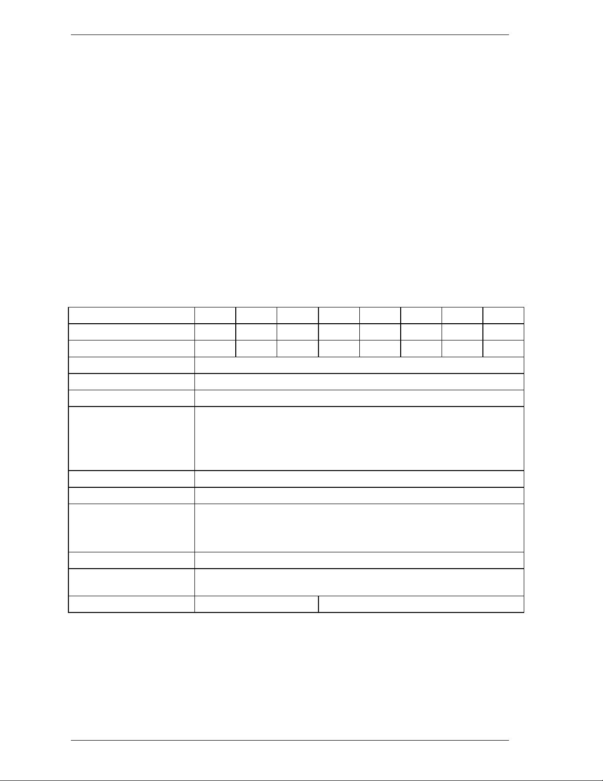
1.2 Device Specifications
1.2.1 Specifications summary
Table 1.1 shows the specifications of the disk drives.
Table 1.1 Specifications (1/2)
Format Capacity (*1, *2)
Number of Sectors (User)
Bytes per Sector 512 bytes
Rotational Speed 5,400 rpm ± 1%
Average Latency 5.56 ms
Positioning time (read and seek)
• Minimum (Track-Track)
• Average
• Maximum (Full)
Start time 4.0 sec (typ.)
Interface Compliant with ATA-8 ACS AST, Serial ATA Revision 2.5 Gen1i
Data Transfer Rate (*3)
• To/From Media
• To/From Host
Data Buffer Size (*4) 8 MB (8,388,608 bytes)
Physical Dimensions
(Height × Width × Depth)
Weight 101 g (Max.) 96 g (Max.)
MHY2250BH MHY2200BH MHY2160BH MHY2120BH MHY2100BH MHY2080BH MHY2060BH MHY2040BH
250 GB 200 GB 160 GB 120 GB 100 GB 80 GB 60 GB 40 GB
488,397,168 390,721,968 312, 581, 808 234,441,648 195,371,568 156,301,488 117,210,240 78,140,160
1.5 ms (typ.)
Read: 12.0 ms (typ.)
22 ms (typ.)
84.6 MB/s Max.
1.5 Gbps (150 MB/s) (Gen1i)
9.5 mm × 100.0 mm × 70.0 mm (*5)
*1: Capacity under the LBA mode.
*2: One gigabyte (GB) = one billion bytes and One megabyte (MB) = one million bytes;
accessible capacity will be less and actual capacity depends on the operating environment and
formatting.
*3: 1 GB is equal to 1,000,000,000 bytes and 1 MB is equal to 1,000,000 bytes.
1-4 C141-E262
Page 29

1.2 Device Specifications
*4: 1 MB is equal to 1,048,576 bytes; the actual buffer capacity for data transfer will be less.
Refer to the Section 6.4 of this manual.
*5: The value of Depth (=100.0 mm) does not include PCBA (Printed Circuit Board Assembly).
For details, see Section 3.1.
Table 1.1 lists the formatted capacity, number of logical cylinders, number of
heads, and number of sectors of every model for which the CHS mode has been
selected using the BIOS setup utility on the host.
Table 1.1 Specifications (2/2)
Model Capacity (*1) No. of Cylinder No. of Heads No. of Sectors
MHY2250BH 8.45 GB 16,383 16 63
MHY2200BH 8.45 GB 16,383 16 63
MHY2160BH 8.45 GB 16,383 16 63
MHY2120BH 8.45 GB 16,383 16 63
MHY2100BH 8.45 GB 16,383 16 63
MHY2080BH 8.45 GB 16,383 16 63
MHY2060BH 8.45 GB 16,383 16 63
MHY2040BH 8.45 GB 16,383 16 63
*1: One gigabyte (GB) = one billion bytes; accessible capacity will be less and actual capacity
depends on the operating environment and formatting.
1.2.2 Model and product number
Table 1.2 lists the model names and product numbers of the disk drive.
The model name does not necessarily correspond to the product number as listed
in Table 1.2 since some models have been customized and have specifications
that are different from those for the standard model.
If a disk drive is ordered as a replacement drive, the product number must be the
same as that of the drive being replaced.
C141-E262 1-5
Page 30

Device Overview
Table 1.2 Examples of model names and product numbers
Model Name
MHY2250BH 250 GB M3 Depth 3 CA06889-B045
MHY2200BH 200 GB M3 Depth 3 CA06889-B040
MHY2160BH 160 GB M3 Depth 3 CA06889-B036
MHY2120BH 120 GB M3 Depth 3 CA06889-B022
MHY2100BH 100 GB M3 Depth 3 CA06889-B020
MHY2080BH 80 GB M3 Depth 3 CA06889-B028
MHY2060BH 60 GB M3 Depth 3 CA06889-B016
MHY2040BH 40 GB M3 Depth 3 CA06889-B014
*1: One gigabyte (GB) = one billion bytes; accessible capacity will be less and actual capacity
depends on the operating environment and formatting.
Capacity (*1)
(user area)
Mounting screw Order No.
1-6 C141-E262
Page 31
1.3 Power Requirements
1.3 Power Requirements
(1) Input Voltage
• + 5 V ± 5 %
• It is unnecessary for this drive to supply +3.3 V and +12 V power supplies.
(2) Ripple
+5 V
Maximum 100 mV (peak to peak)
Frequency DC to 1 MHz
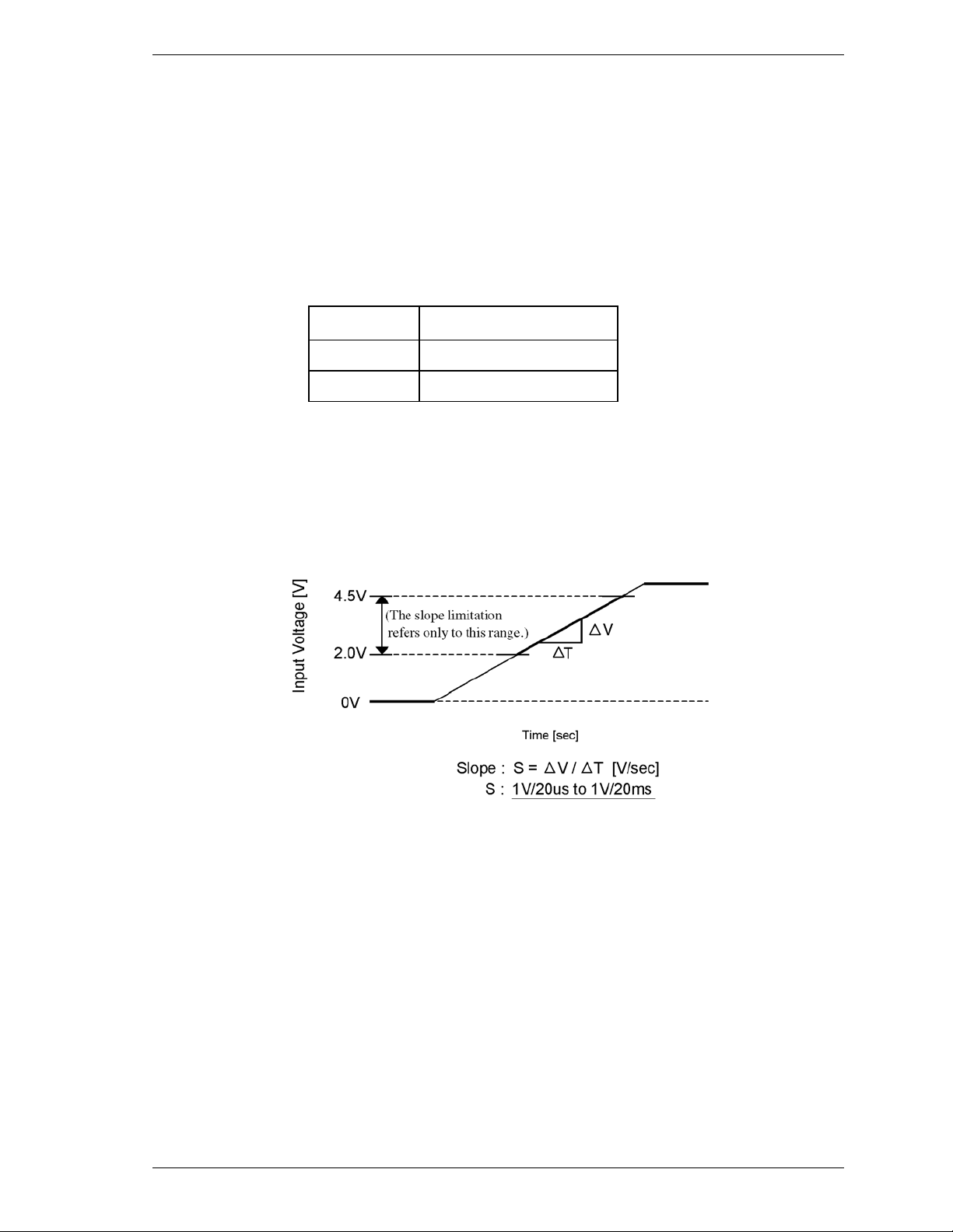
(3) Slope of an input voltage at rise
The following figure shows the restriction of the slope which is +5 V input
voltage at rise. The permissible range of +5 V slope is from 1V/20 µsec to
1V/20 msec, under the voltage range is between 2.0V and 4.5V.
Figure 1.1 Permissible range of +5V rise slope
C141-E262 1-7
Page 32
Device Overview
(4) A negative voltage like the bottom figure isn't t o occur at +5 V when power is turned
off and, a thing with no ringing.
Permissible level: − 0.2 V
5
4
3
2
Voltage [V]
1
0
-1
0 100 200 300 400 500 600 700 800
Time [ms]
Figure 1.2 The example of negative voltage waveform at +5 V
when power is turned off
1-8 C141-E262
Page 33

1.3 Power Requirements
(5) Current Requirements and Power Dissipation
Table 1.3 lists the current and power dissipation (typical).
Table 1.3 Current and power dissipation
Typical RMS Current Typical Power (*3)
Spin up (*1) 1.0 A 5.0 W
Idle (*6) 120 mA 0.60 W
R/W (on track) (*2) 380 mA 1.9 W
Seek (*5) 420 mA 2.1 W
Standby (*6) 26 mA 0.13 W
Sleep (*6) 26 mA 0.13 W
e rank (0.0024 W/GB): MHY2250BH
e rank (0.0030 W/GB): MHY2200BH
Energy
Efficiency (*4)
e rank (0.0038 W/GB): MHY2160BH
d rank (0.0050 W/GB): MHY2120BH
⎯
d rank (0.0060 W/GB): MHY2100BH
d rank (0.0075 W/GB): MHY2080BH
d rank (0.0100 W/GB): MHY2060BH
d rank (0.0150 W/GB): MHY2040BH
*1 Maximum current and power at starting spindle motor.
*2 Current and power level when the operation (command) that accompanies a
transfer of 63 sectors is executed 3 times in 100 ms
*3 Power requirements reflect typical values for +5 V power.
*4 Energy efficiency based on the Law concerning the Rational Use of Energy
indicates the value obtained by dividing power consumption by the storage
capacity. (Japan only)
*5 The seek average current is specified based on three operations per 100
msec.
*6 IPM mode: Slumber mode.
C141-E262 1-9
Page 34

Device Overview
(6) Current fluctuation (Typ.) at +5 V when power is turned on
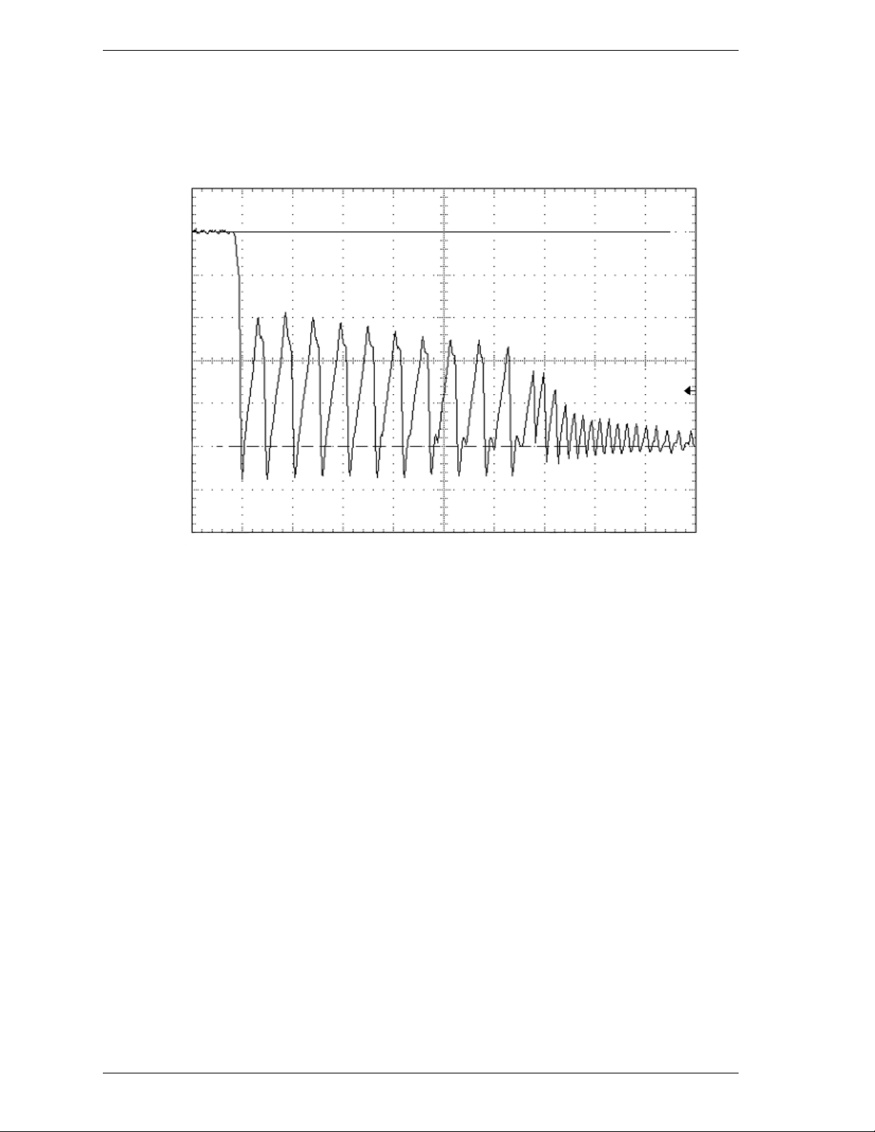
Figure 1.3 Current fluctuation (Typ.) at +5 V when power is turned on
1.4 Environmental Specifications
Table 1.4 lists the environmental specifications.
Table 1.4 Environmental specificati ons
Item Specification
Temperature
• Operating
• Non-operating
• Thermal Gradient
Humidity
• Operating
• Non-operating
• Maximum Wet Bulb
Altitude (relative to sea level)
• Operating
• Non-operating
5 °C to 55 °C (ambient)
5 °C to 60 °C (disk enclosure surface)
–40 °C to 65 °C
20 °C/h or less
8 % to 90 % RH (Non-condensing)
5 % to 95 % RH (Non-condensing)
29 °C (Operating)
40 °C (Non-operating)
–300 to 3,000 m
–300 to 12,000 m
1-10 C141-E262
Page 35

1.5 Acoustic Noise
1.5 Acoustic Noise
Table 1.5 lists the acoustic noise specification.
Table 1.5 Acoustic noise specification
Item Specification
• Idle mode (DRIVE READY)
Sound Power
Sound Pressure (at 0.3m)
2.0B [MHY2120BH, MHY2100BH, MHY2080BH,
MHY2060BH, MHY2040BH]
2.4B [MHY2250BH, MHY2200BH, MHY2160BH]
22dB [MHY2120BH, MHY2100BH, MHY2080BH,
MHY2060BH, MHY2040BH]
28dB [MHY2250BH, MHY2200BH, MHY2160BH]
Note:
Measure the noise from the cover top surface.
1.6 Shock and Vibration
Table 1.6 lists the shock and vibration specification.
Table 1.6 Shock and vibration specification
Item Specification
Vibration (Swept sine, 1/4 octave per minute)
• Operating
Non-operating
2
5 to 500 Hz, 9.8m/s
0-peak (1G 0-peak)
(without non-recovered errors)
5 to 500 Hz, 49m/s
2
0-peak (5G 0-peak)
(no damage)
Shock (half-sine pulse)
• Operating
• Non-operating
2
3185 m/s
0-peak (325G 0-peak)
2ms duration
(without non-recovered errors)
2
8820 m/s
0-peak (900G 0-peak)
1ms duration
2
1176 m/s
0-peak (120G 0-peak)
11ms duration
(no damage)
C141-E262 1-11
Page 36

Device Overview
1.7 Reliability
(1) Mean time between failures (MTBF)
Conditions of 300,000 h Power-on time 250H/month or less 3000H/years
or less
Operating time 20 % or less of power-on time
Temperature
Humidity
MTBF is defined as follows:
Total operation time in all fields
MTBF= (H)
number of device failure in all fields (*1)
*1 "Disk drive defects" refers to defects that involve repair, readjustment, or
replacement. Disk drive defects do not include failures caused by external
factors, such as damage caused by handling, inappropriate operating
environments, defects in the power supply host system, or interface cable.
5 to 60 °C (Disk Enclosure surface)
8 to 90 % (ambient)
But humidity bulb temperature
29 °C or less
(2) Mean time to repair (MTTR)
The mean time to repair (MTTR) is 30 minutes or less, if repaired by a specialist
maintenance staff member.
(3) Service life
In situations where management and handling are correct, the disk drive requires
no overhaul for five years when the DE surface temperature is less than 48 °C.
When the DE surface temperature exceeds 48 °C, the disk drives requires no
overhaul for five years or 20,000 hours of operation, whichever occurs first.
Refer to item (3) in Subsection 3.2 for the measurement point of the DE surface
temperature. The operating conditions of Service life are based on the equal
conditions with MTBF.
(4) Data assurance in the event of power failure
Except for the data block being written to, the data on the disk media is assured in
the event of any power supply abnormalities. This does not include power supply
abnormalities during disk media initialization (formatting) or processing of
defects (alternative block assignment).
1-12 C141-E262
Page 37

1.8 Error Rate
1.8 Error Rate
Known defects, for which alternative blocks can be assigned, are not included in
the error rate count below. It is assumed that the data blocks to be accessed are
evenly distributed on the disk media.
(1) Unrecoverable read error
Read errors that cannot be recovered by maximum read retries of drive without
user's retry and ECC corrections shall occur no more than 1 time when reading
data of 10
recovery procedure, and include read retries accompanying head offset
operations.
(2) Positioning error
14
bits. Read retries are executed according to the disk drive's error
Positioning (seek) errors that can be recovered by one retry shall occur no more
than 1 time in 10
7
seek operations.
1.9 Media Defects
Defective sectors are replaced with alternates when the disk drive is formatted
prior to shipment from the factory (low level format). Thus, the hosts see a
defect-free device.
Alternate sectors are automatically accessed by the disk drive. The user need not
be concerned with access to alternate sectors.
1.10 Load/Unload Function
The Load/Unload function is a mechanism that loads the head on the disk and
unloads the head from the disk.
The product supports a minimum of 600,000 Load/Unload cycles.
Unload is a normal head unloading operation and the commands listed below are
executed.
• STANDBY command issued
• STANDBY IMMEDIATE command issued
• SLEEP command issued
• IDLE IMMEDIATE command (with unload feature) issued
• Power Mode shifted with APM or APS feature.
• SLUMBER signal transferred
(PMREQ_S signal is transferred from the host or the drive, and the host
responds with PMACK signal.)
C141-E262 1-13
Page 38

Device Overview
Emergency Unload other than Unload is performed when the power is shut down
while the heads are still loaded on the disk.
The product supports the Emergency Unload a minimum of 20,000 times.
When the power is shut down, the controlled Unload cannot be executed.
Therefore, the number of Emergency other than Unload is specified.
1.10.1 Recommended power-off sequence
We recommend cutting the power supply of the HDD for this device after the
Head Unload operation completes. The recommended power supply cutting
sequence for this device is as follows:
1) Disk Flush
Flush Cache command execution.
2) Head Unload
Standby Immediate command execution.
3) Wait Status
Checking whether bit 7 of the status register was set to '0'.
(wait to complete STANDBY IMMEDIATE command)
4) HDD power supply cutting
1.11 Advanced Power Management (APM)
The disk drive automatically shifts to the power saving mode according to the
setting of the APM mode under the idle condition.
The APM mode can be chosen with a Sector Count register of the SET
FEATURES (EF) command.
The disk drive complies with the three kinds of APM modes that a command
from the host is required.
FR = 05h : Enable APM
SC = C0h - FEh :
SC = 80h - BFh :
Mode-0 Active Idle → Low Power Idle
Mode-1 Active Idle → Low Power Idle (Default)
SC = 01h - 7Fh :
FR = 85h : Disable APM (Set Mode-0)
Active Idle: The head is in a position of extreme inner in disk
1-14 C141-E262
Mode-2 Active Idle → Low Power Idle → Standby
medium. (VCM Lock)
Page 39

1.11 Advanced Power Management (APM)
Low Power Idle: The head is unloaded from disk.
The spindle motor rotates.
Standby: The spindle motor stops.
In APM Mode-1, which is the APM default mode, the operation status shifts till it
finally reaches "Low Power Idle."
Table 1.7 Advanced Power Management
APM Mode
Active Idle
(VCM Lock)
Low Power Idle
(Unload)
Standby
(Spin Off)
Mode-0 0.2-1.2 sec 15 min. N/A
Mode-1 0.1-0.2 sec 10.0-27.5 sec N/A
Mode-2 0.1-0.2 sec 10.0-27.5 sec 10.0-40.0 sec
When the maximum time that the HDD is waiting for commands has been
exceeded:
Mode-0: Mode shifts from Active condition to Active Idle in 0.2-1.2, and to Low
Power Idle in 15 minutes.
Mode-1: Mode shifts from Active condition to Active Idle in 0.1-0.2 seconds and
to Low Power Idle in 10.0-27.5 seconds.
Mode-2: Mode shifts from Active condition to Active Idle in 0.1-0.2 seconds and
to Low Power Idle in 10.0-27.5 seconds. After 10.0-40.0 seconds in
Low Power Idle, the mode shifts to standby.
Remark:
The default values of these settings are reflected in the WORD 91 values of the
IDENTIFY DEVICE command. Also, the APM mode is initialized to Mode-1
(default value) at power-off.
The above mentioned is time until shifting to each power mode based on point
that the drive becomes a command waiting state.
C141-E262 1-15
Page 40

Device Overview
1.12 Interface Power Management (IPM)
1.12.1 Host-initiated interface power management (HIPM)
When the disk drive is waiting for commands, it can enter one of three IPM
modes as requested by the host. The three IPM modes are:
1) Partial mode: PMREQ_P is sent when the host requests the Partial mode.
2) Slumber mode: PMREQ_S is sent when the host requests the Slumber mode.
3) Active mode: When the serial ATA interface is in active state.
There are three interface (I/F) power states: Active, Partial, and Slumber. As
requested by the host, the disk drive switches its I/F power state from the Active
state to the Partial state, or from the Active state to the Slumber state.
1.12.2 Device-initiated interface power management (DIPM)
If this function is enabled by Set Features command, the disk drive shifts to two
kinds of IPM modes automatically under the Idle condition.
1) Partial mode: PMREQ_P is sent when the disk drive requests the Partial
mode.
2) Slumber mode: PMREQ_S is sent when the disk drive requests the Slumber
mode.
I/F power states
1) Active state
The SATA interface is active, and data can be sent and received.
2) Partial state
The SATA interface is in the Power Down state. In this state, the interface is
switched to the Partial state when a PMREQ_P signal is received from or sent
to host. Because the return time to the Active state from the Partial state is
specified as within 10 µs, the degree of the I/F Power Save mode is shallow
so that this recovery time is satisfied.
3) Slumber state
The SATA interface is in the Power Down state. In this state, the interface is
switched to the Slumber state when a PMREQ_S signal is received from or
sent to host. Because the return time to the Active state from the Slumber
state is specified as within 10 ms, the degree of the I/F Power Save mode is
deep so that this recovery time is satisfied.
1-16 C141-E262
Page 41

1.12 Interface Power Management (IPM)
Table 1.8 Interface power management
IPM Mode I/F power state Return time to active I/F condition
Active Active State
Partial Partial State
Slumber Slumber State 5 to 10 ms maximum Power Down
5 to 10 µs maximum
−
Active
Power Down
C141-E262 1-17
Page 42

This page is intentionally
left blank.
Page 43

CHAPTER 2 Device Configuration
2.1 Device Configuration
2.2 System Configuration
This chapter describes the internal configurations of the hard disk drives and the
configuration of the systems in which they operate.
C141-E262 2-1
Page 44

Device Configuration
2.1 Device Configuration
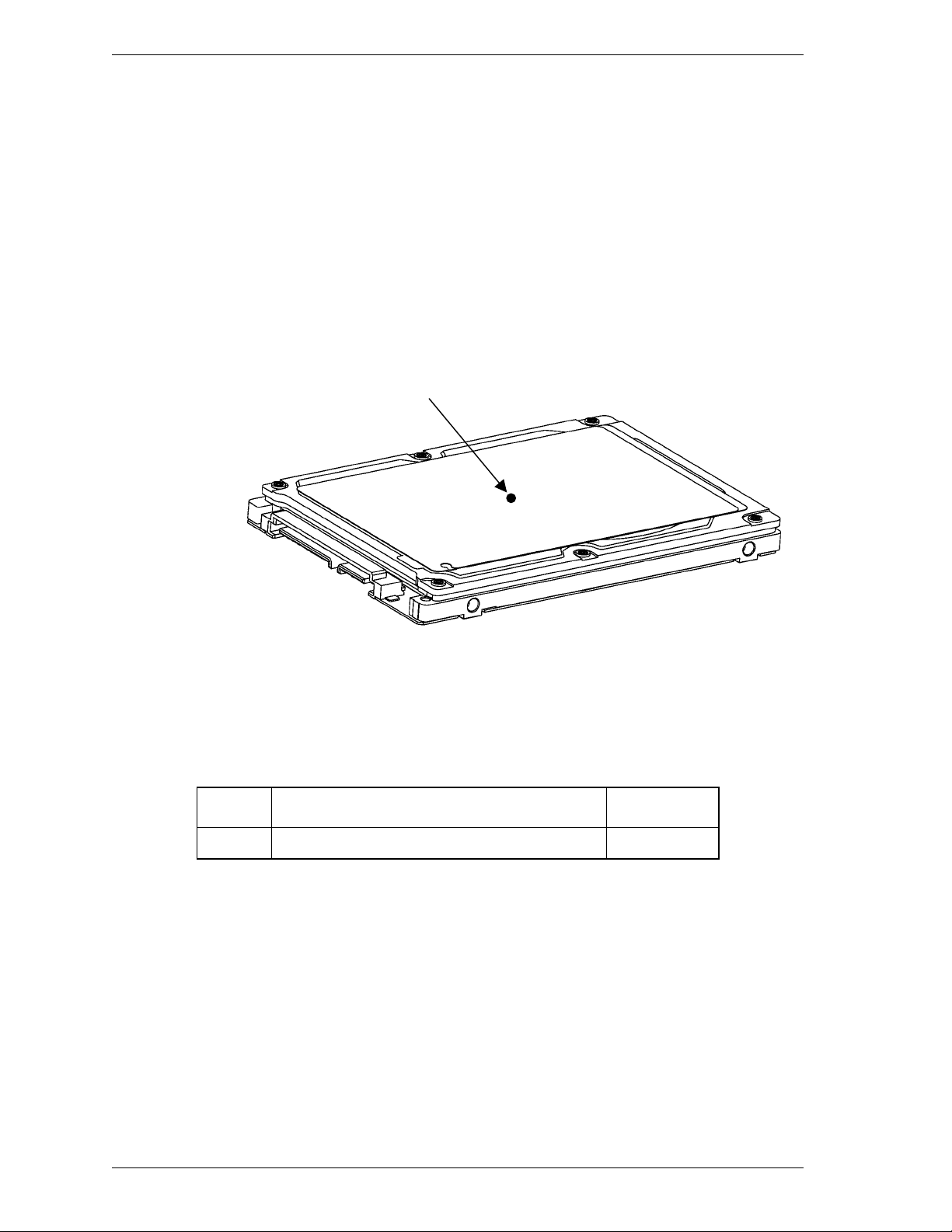
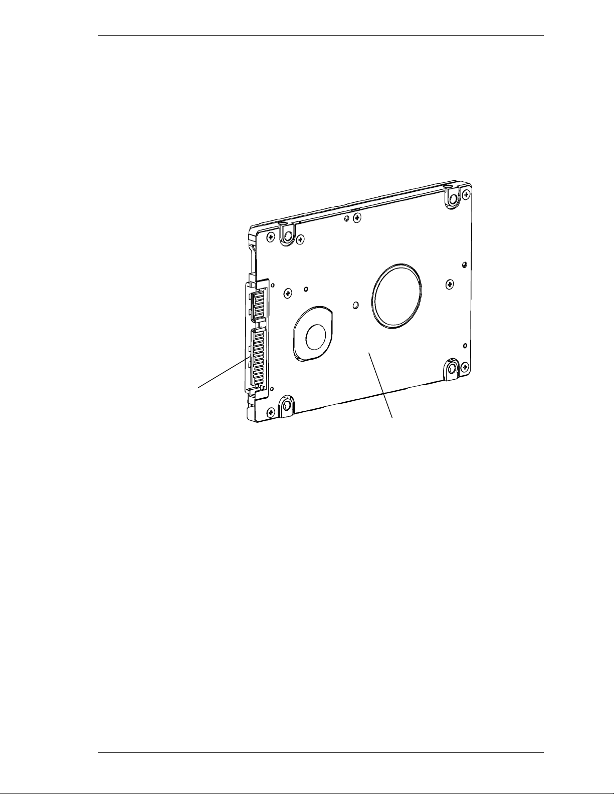
Figure 2.1 shows the disk drive. The disk drive consists of a disk enclosure (DE),
read/write preamplifier, and controller PCA. The disk enclosure contains the disk
media, heads, spindle motor, actuator, and a circulating air filter.
(1) Disk
The outer diameter of the disk is 65 mm. The inner diameter is 20 mm.
(2) Head
The heads are of the load/unload (L/UL) type. The head unloads the disk out of
while the disk is not rotating and loads on the disk when the disk starts.
(3) Spindle motor
The disks are rotated by a direct drive Sensor-less DC motor.
(4) Actuator
The actuator uses a revolving voice coil motor (VCM) structure which consumes
low power and generates very little heat. The head assembly at the edge of the
actuator arm is controlled and positioned by feedback of the servo information
read by the read/write head. If the power is not on or if the spindle motor is
stopped, the head assembly stays on the ramp out of the disk and is fixed by a
mechanical lock.
Figure 2.1 Disk drive outerview
2-2 C141-E262
Page 45

2.2 System Configuration
(5) Air circulation system
The disk enclosure (DE) is sealed to prevent dust and dirt from entering. The
disk enclosure features a closed loop air circulation system that relies on the
blower effect of the rotating disk. This system continuously circulates the air
through the circulation filter to maintain the cleanliness of the air within the disk
enclosure.
(6) Read/write circuit
The read/write circuit uses a LSI chip for the read/write preamplifier. It improves
data reliability by preventing errors caused by external noise.
(7) Controller circuit
The controller circuit supports Serial-ATA interface, and it realized a high
performance by integration into LSI.
2.2 System Configuration
2.2.1 SATA interface
Figure 2.2 shows the SATA interface system configuration. The disk drive
complies with ATA-8 ACS AST, Serial ATA Revision 2.5 (Gen1i).
2.2.2 Drive connection
Operating System
Application 1
Application 2
Application 3
Driver
Serial
ATA
Adapter
Disk Drive
Disk Drive
Figure 2.2 Drive system configuration
C141-E262 2-3
Page 46

This page is intentionally
left blank.
Page 47

CHAPTER 3 Installation Conditions
3.1 Dimensions
3.2 Mounting
3.3 Connections with Host System
This chapter gives the external dimensions, installation conditions, surface
temperature conditions, cable connections, and switch settings of the hard disk
drives.
C141-E262 3-1
Page 48
Installation Conditions
3.1 Dimensions
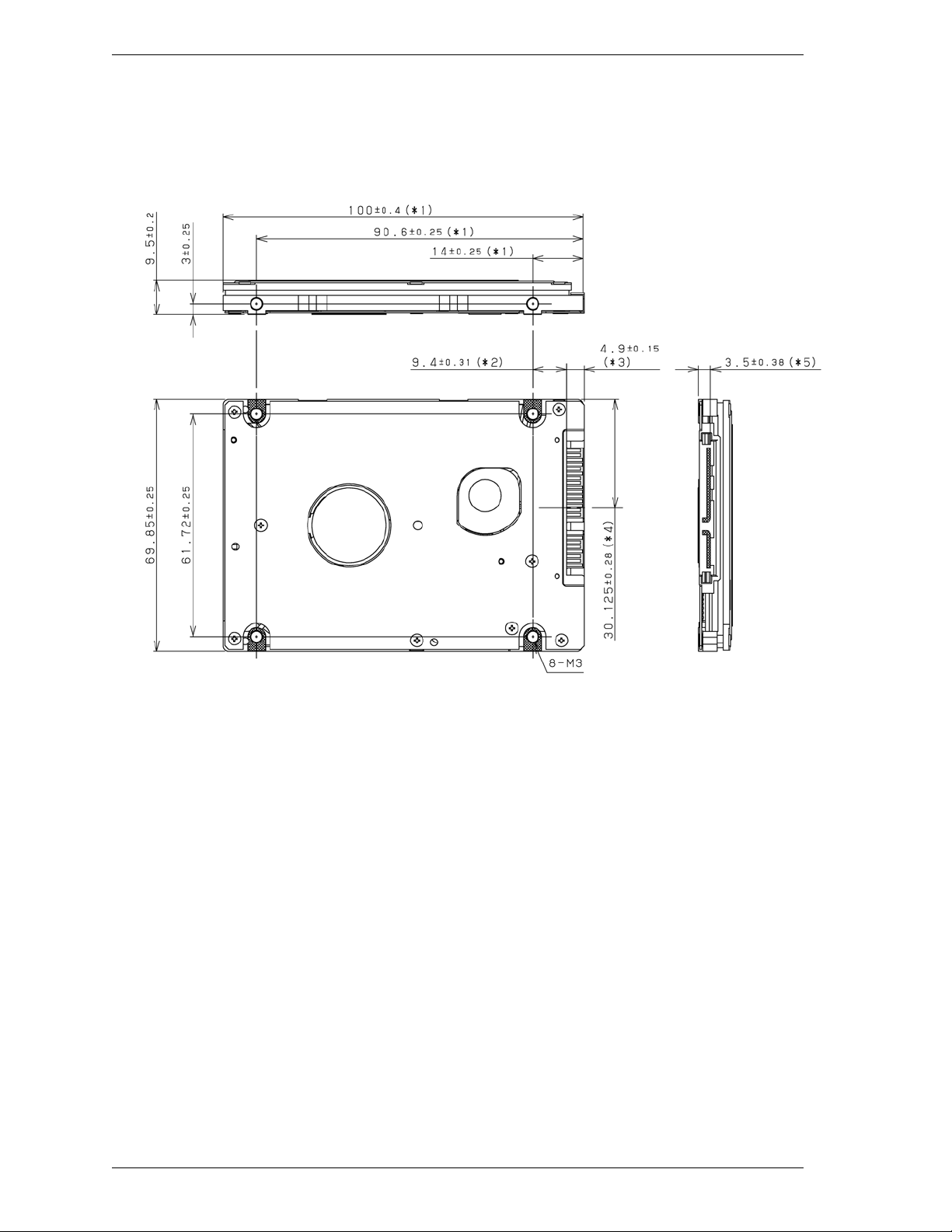
Figure 3.1 illustrates the dimensions of the disk drive. All dimensions are in mm.
*1 The PCA and connectors are not included in these dimensions.
*2 Dimension from the center of the user tap to the base of the connector pins
*3 Length of the connector pins
*4 Dimension from the outer edge of the user tap to the center of the connector
pins
*5 Dimension from the outer edge of the user tap to the innermost edge of the
connector pins
Figure 3.1 Dimensions
3-2 C141-E262
Page 49

3.2 Mounting
3.2 Mounting
For information on mounting, see the "FUJITSU 2.5-INCH HDD
INTEGRATION GUIDANCE (C141-E144)."
(1) Orientation
The disk drives can be mounted in any direction.
(2) Frame
The MR head bias of the HDD disk enclosure (DE) is zero. The mounting frame
is connected to Signal Ground (SG).
Use M3 screw for the mounting screw and the screw length should
satisfy the specification in Figure 3.2.
The tightening torque must be 0.49N
When attaching the HDD to the system frame, do not allow the
system frame to touch parts (cover and base) other than parts to
which the HDD is attached.
•m (5kgf•cm).
C141-E262 3-3
Page 50
Installation Conditions
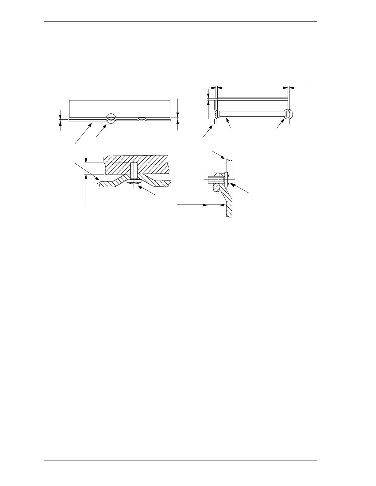
(3) Limitation of mounting
Note) These dimensions are recommended values; if it is not possible to satisfy
them, contact us.
Bottom surface mounting
Side surface
mounting
2.5 2.5
2
A
Frame of system
cabinet
3.0 or less
DE
2.5
2.5
Frame of system
cabinet
Screw
3.0 or less
Details of A
Figure 3.2 Mounting frame structure
PCA
B
Screw
3-4 C141-E262
Page 51

3.2 Mounting
Because of breather hole mounted to the HDD, do not allow this to
close during mounting.
Locating of breather hole is shown as Figure 3.3.
For breather hole of Figure 3.3, at least, do not allow its around
φ 3
to block.
Figure 3.3 Location of breather
C141-E262 3-5
Page 52
Installation Conditions
(4) Ambient temperature
The temperature conditions for a disk drive mounted in a cabinet refer to the
ambient temperature at a point 3 cm from the disk drive. The ambient
temperature must satisfy the temperature conditions described in Section 1.4, and
the airflow must be considered to prevent the DE surface cover temperature from
exceeding 60
°C.
Provide air circulation in the cabinet such that the PCA side, in particular,
receives sufficient cooling. To check the cooling efficiency, measure the surface
cover temperatures of the DE. Regardless of the ambient temperature, this
surface cover temperature must meet the standards listed in Table 3.1. Figure 3.4
shows the temperature measurement point.
1
Figure 3.4 Surface cover temperature measurement points
Table 3.1 Surface temperature measurement points and standard values
No. Measurement point Temperature
1 DE cover
°C max
60
3-6 C141-E262
Page 53

3.2 Mounting
(5) Service area
Figure 3.5 shows how the drive must be accessed (service areas) during and after
installation.
Mounting screw hole
Cable connection
Figure 3.5 Service area
Mounting screw hole
Data corruption: Avoid mounting the disk drive near strong
magnetic sources such as loud speakers. Ensure that the disk drive
is not affected by external magnetic fields.
Damage: Do not press the cover of the disk drive. Pressing it too
hard, the cover and the spindle motor contact, which may cause
damage to the disk drive.
Static: When handling the device, disconnect the body ground
Ω or greater). Do not touch the printed circuit board, but
(500 k
hold it by the edges.
(6) Handling cautions
Please keep the following cautions, and handle the HDD under the safety
environment.
C141-E262 3-7
Page 54

Installation Conditions
p
ying
p
g
p
- General notes
ESD mat
Wrist strap
Use the Wrist stra
Do not hit HDD each other.
Do not
to avoid fallin
lace HDD vertically
.
down.
Shock absorbing mat
Place the shock absorbing mat on the
operation table, and place ESD mat on it.
Do not stack when carr
Do not dro
.
.
Figure 3.6 Handling cautions
- Installation
(1) Please use the driver of a low impact when you use an electric driver.
HDD is occasionally damaged by the impact of the driver.
(2) Please observe the tightening torque of the screw strictly.
⋅⋅⋅⋅⋅⋅ 0.49N • m (5 kgf • cm).
M3
-
Recommended equipments
Contents Model Maker
Wrist strap JX-1200-3056-8 SUMITOMO 3M ESD
ESD mat SKY-8A (Color Seiden Mat) Achilles
Shock Low shock driver SS-6500 HIOS
3-8 C141-E262
Page 55
3.3 Connections with Host System
3.3 Connections with Host System
3.3.1 Device connector
The disk drive has the SATA interface connectors listed below for connecting
external devices. Figure 3.7 shows the locations of these connectors and
terminals.
SATA interface
and power
connectors
PCA
Figure 3.7 Connector locations
C141-E262 3-9
Page 56

Installation Conditions
3.3.2 Signal segment and power supply segment
Figure 3.8 shows each segment of the SATA interface connector and pin
numbers.
View from the
connector side
Power supply
segment
P1 pins in the power
supply segment
Signal segment
S1 pins in the signal
segment
Figure 3.8 Power supply pins (CN1)
3.3.3 Connector specifications for host system
The connector of host system for mating with the disk drive must be compliant
with Serial-ATA Revision 2.5 specification. For detail of requirements about
SATA interface connector, refer to the "Serial-ATA Revision 2.5."
View from the
PCA side
The connection reliability per number of insertion/extractions varies
with the condition of the connection with the host system.
Therefore, we recommend that the customer evaluate the connector
on the customer's system and select it from the connectors
complying with the Serial ATA Revision 2.5 specification.
3-10 C141-E262
Page 57

3.3 Connections with Host System
3.3.4 SATA interface cable connection
The cable that connects the disk drive to the host system must be compliant with
the Serial ATA Revision 2.5 specification.
3.3.5 Note about SATA interface cable connection
Take note of the following precaution about plugging a SATA interface cable into
the SATA interface connector of the disk drive and plugging the connector into a
host receptacle:
When plugging together the disk drive SATA interface connector
and the host receptacle or SATA interface cable connector, do not
apply more than 10 kgf of force in the connection direction once
they are snugly and securely in position.
Removing the cable without releasing the SATA interface Latch
may lead to connector damage and the loss of the Latch function.
Accordingly, be sure to remove the cable while releasing the Latch.
C141-E262 3-11
Page 58

This page is intentionally
left blank.
Page 59

CHAPTER 4 Theory of Device Operation
4.1 Outline
4.2 Subassemblies
4.3 Circuit Configuration
4.4 Power-on Sequence
4.5 Self-calibration
4.6 Read/write Circuit
4.7 Servo Control
This chapter explains basic design concepts of the disk drive. Also, this chapter
explains subassemblies of the disk drive, each sequence, servo control, and
electrical circuit blocks.
C141-E262 4-1
Page 60

Theory of Device Operation
4.1 Outline
This chapter consists of two parts. First part (Section 4.2) explains mechanical
assemblies of the disk drive. Second part (Sections 4.3 through 4.7) explains a
servo information recorded in the disk drive and drive control method.
4.2 Subassemblies
The disk drive consists of a disk enclosure (DE) and printed circuit assembly
(PCA).
The DE contains all movable parts in the disk drive, including the disk, spindle,
actuator, read/write head, and air filter. For details, see Subsections 4.2.1 to 4.2.4.
The PCA contains the control circuits for the disk drive. The disk drive has one
PCA. For details, see Sections 4.3.
4.2.1 Disk
The DE contains disks with an outer diameter of 65 mm and an inner diameter of
20 mm.
Servo data is recorded on each cylinder (total 162). Servo data written at factory
is read out by the read head. For servo data, see Section 4.7.
4.2.2 Spindle
The spindle consists of a disk stack assembly and spindle motor. The disk stack
assembly is activated by the direct drive sensor-less DC spindle motor, which has
a speed of 5,400 rpm ±1%. The spindle is controlled with detecting a PHASE
signal generated by counter electromotive voltage of the spindle motor at starting.
4.2.3 Actuator
The actuator consists of a voice coil motor (VCM) and a head carriage. The
VCM moves the head carriage along the inner or outer edge of the disk. The head
carriage position is controlled by feeding back the difference of the target position
that is detected and reproduced from the servo information read by the read/write
head.
4-2 C141-E262
Page 61

4.2.4 Air filter
There are two types of air filters: a breather filter and a circulation filter.
The breather filter makes an air in and out of the DE to prevent unnecessary
pressure around the spindle when the disk starts or stops rotating. When disk
drives are transported under conditions where the air pressure changes a lot,
filtered air is circulated in the DE.
The circulation filter cleans out dust and dirt from inside the DE. The disk drive
cycles air continuously through the circulation filter through an enclosed loop air
cycle system operated by a blower on the rotating disk.
4.3 Circuit Configuration
Figure 4.1 shows the power supply configuration of the disk drive, and Figure 4.2
shows the disk drive circuit configuration.
(1) Read/write circuit
4.3 Circuit Configuration
The read/write circuit consists of two circuits; read/write preamplifier (PreAMP)
and read channel (RDC) which is integrated into LSI with MCU and HDC.
The PreAMP consists of the write current switch circuit, that flows the write
current to the head coil, and the voltage amplifier circuit, that amplitudes the read
output from the head.
The RDC is the read demodulation circuit using the Modified Extended Partial
Response (MEEPR), and contains the Viterbi detector, programmable filter,
adaptable transversal filter, times base generator, data separator circuits,
RLL (Run Length Limited) encoder and servo demodulation circuit.
(2) Servo circuit
The position and speed of the voice coil motor are controlled by closed-loop servo
using the servo information recorded on the data surface. The servo information
is an analog signal converted to digital for processing by a MPU and then
reconverted to an analog signal for control of the voice coil motor.
The MPU precisely sets each head on the track according on the servo
information on the media surface.
(3) Spindle motor driver circuit
The circuit measures the interval of a PHASE signal generated by counterelectromotive voltage of a motor and controls the motor speed comparing target
speed.
C141-E262 4-3
Page 62
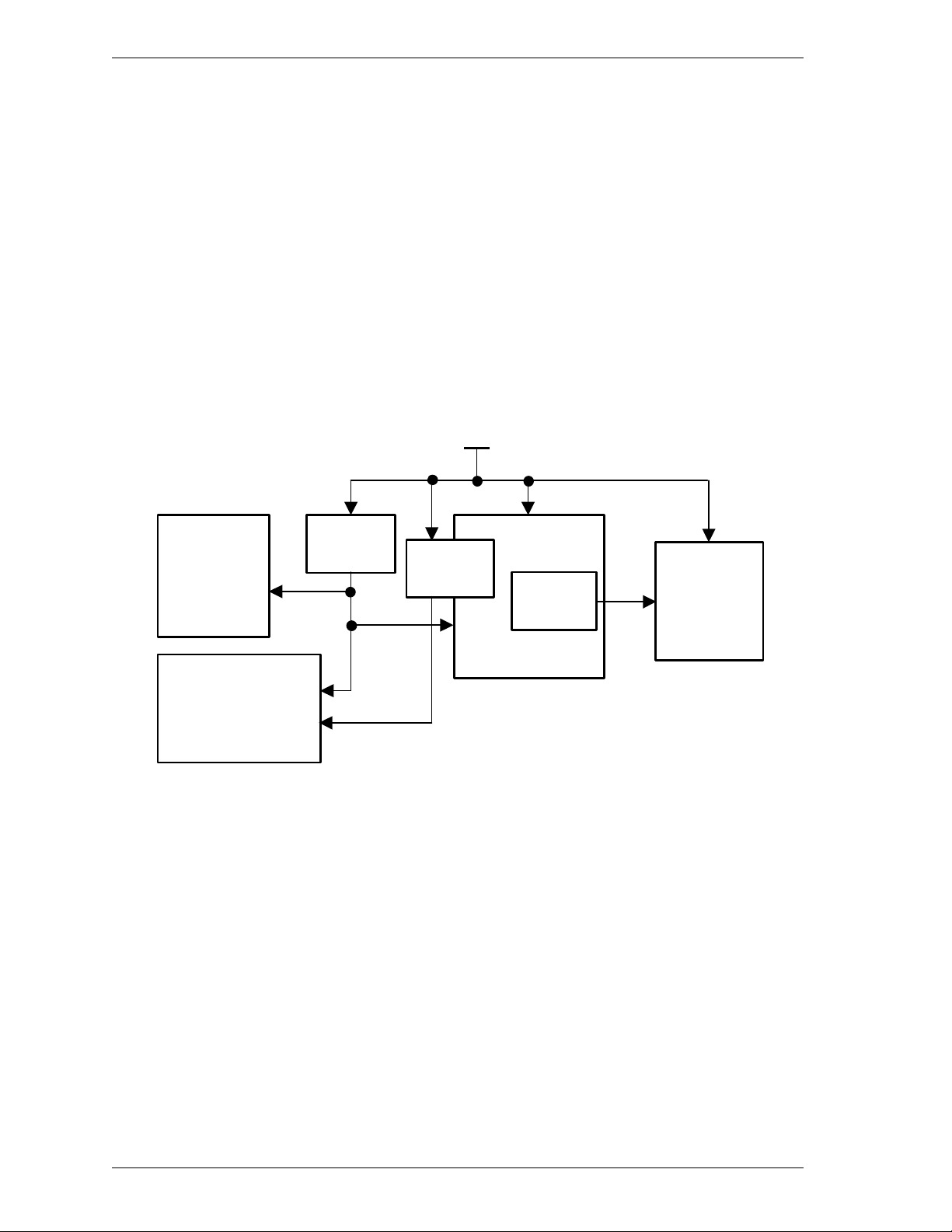
Theory of Device Operation
(4) Controller circuit
Major functions are listed below.
• Serial-ATA interface control and data transfer control
• Data buffer management
• Sector format control
• Defect management
• ECC control
• Error recovery and self-diagnosis
5.0V
S-DRAM SVC 3.3V
Generator
Circuit
MCU & HDC & RDC
Integration
Figure 4.1 Power supply configuration
3.3V
1.2V
1.2V
Generator
Circuit
-3V
Generator
Circuit
PreAMP
-3.0V
4-4 C141-E262
Page 63
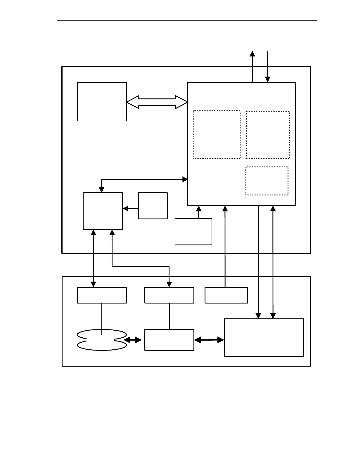
PCA
4.3 Circuit Configuration
Serial-ATA Interface
Data Buffer
SDRAM
SVC
Shock
Sensor
Crystal
MCU & HDC & RDC
MCU
HDC
RDC
DE
SP Motor
Media
VCM
HEAD
Figure 4.2 Circuit configuration
Thermistor
R/W Pre-Amp
C141-E262 4-5
Page 64

Theory of Device Operation
4.4 Power-on Sequence
Figure 4.3 describes the operation sequence of the disk drive at power-on. The
outline is described below.
a) After the power is turned on, the disk drive initializes its SATA interface
block.
b) The disk drive executes the MPU bus test, internal register read/write test,
and work RAM read/write test. When the self-diagnosis terminates
successfully, the disk drive starts the spindle motor.
c) The disk drive executes self-diagnosis (data buffer read/write test).
d) After confirming that the spindle motor has reached rated speed, the head
assembly is loaded on the disk.
e) The disk drive positions the heads onto the SA area and reads out the system
information.
f) The drive becomes ready. The host can issue commands.
g) The disk drive executes self -calibration. This collects data for VCM torque
and mechanical external forces applied to the actuator, and updates the
calibrating value.
4-6 C141-E262
Page 65

Power-on
4.4 Power-on Sequence
Start
a)
b)
c)
d)
SATA I/F Initialization
Self-diagnosis 1
- MPU bus test
- Internal regist er
write/read test
- Work RAM write/read
test
The spind le motor starts.
Self-diagnosis 2
- Data buffer write/ read
test
Confirming spindle motor
speed
Load the head assembly
e)
f)
g)
Initial on-track and read
out of system information
Drive ready state
(command waiting state)
Execute self-calibration
End
Figure 4.3 Power-on operation sequence
C141-E262 4-7
Page 66

Theory of Device Operation
4.5 Self-calibration
The disk drive occasionally performs self-calibration in order to sense and
calibrate mechanical external forces on the actuator, and VCM torque. This
enables precise seek and read/write operations.
4.5.1 Self-calibration contents
(1) Sensing and compensating for external forces
The actuator suffers from torque due to the FPC forces and winds accompanying
disk revolution. The torque varies with the disk drive and the cylinder where the
head is positioned. To execute stable fast seek operations, external forces are
occasionally sensed.
The firmware of the drive measures and stores the force (value of the actuator
motor drive current) that balances the torque for stopping head stably. This
includes the current offset in the power amplifier circuit and DAC system.
The forces are compensated by adding the measured value to the specified current
value to the power amplifier. This makes the stable servo control.
To compensate torque varying by the cylinder, the disk is divided into 13 areas
from the innermost to the outermost circumference and the compensating value is
measured at the measuring cylinder on each area at factory calibration. The
measured values are stored in the SA cylinder. In the self-calibration, the
compensating value is updated using the value in the SA cylinder.
(2) Compensating open loop gain
Torque constant value of the VCM has dispersion for each drive, and varies
depending on the cylinder that the head is positioned. To realize the high speed
seek operation, the value that compensates torque constant value change and loop
gain change of the whole servo system due to temperature change is measured
and stored.
For sensing, the firmware mixes the disturbance signal to the position signal at the
state that the head is positioned to any cylinder. The firmware calculates the loop
gain from the position signal and stores the compensation value against to the
target gain as ratio.
For compensating, the direction current value to the power amplifier is multiplied
by the compensation value. By this compensation, loop gain becomes constant
value and the stable servo control is realized.
4-8 C141-E262
Page 67

To compensate torque constant value change depending on cylinder, whole
cylinders from most inner to most outer cylinder are divided into 13 partitions at
calibration in the factory, and the compensation data is measured for
representative cylinder of each partition. This measured value is stored in the SA
area. The compensation value at self-calibration is calculated using the value in
the SA area.
4.5.2 Execution timing of self-calibration
Self-calibration is performed once when power is turned on. After that, the disk
drive does not perform self-calibration until it detects an error.
That is, self-calibration is performed each time one of the following events occur:
• In the case that the disk drive starts up normally, the first part of self-
calibration starts after a lapse of 100 msec. The execution of first part is
about 150 msec. length. The remains is executed thereafter the transfer to
Active-Idle state which takes about 200 msec.
The latter is interrupted when the disk drive receives a Host command, and it
resumes after next transfer to Active-Idle state.
4.5 Self-calibration
• The number of retries to write or seek data reaches the specified value.
• The error rate of data reading, writing, or seeking becomes lower than the
specified value.
4.5.3 Command processing during self-calibration
This enables the host to execute the command without waiting for a long time,
even when the disk drive is performing self-calibration. The command execution
wait time is about maximum 72 ms.
When the error rate of data reading, writing, or seeking becomes lower than the
specified value, self-calibration is performed to maintain disk drive stability.
If the disk drive receives a command execution request from the host while
performing self-calibration, it stops the self-calibration and starts to execute the
command. In other words, if a disk read or write service is necessary, the disk
drive positions the head to the track requested by the host, reads or writes data,
and then restarts calibration after about 3 seconds.
If the error rate recovers to a value exceeding the specified value, self-calibration
is not performed.
C141-E262 4-9
Page 68

Theory of Device Operation
4.6 Read/write Circuit
The read/write circuit consists of the read/write preamplifier (PreAMP), the write
circuit, the read circuit, and the time base generator in the read channel (RDC)
block which is integrated into LSI. Figure 4.4 is a block diagram of the read/write
circuit.
4.6.1 Read/write preamplifier (PreAMP)
PreAMP equips a read preamplifier and a write current switch, that sets the bias
current to the MR device and the current in writing. Each channel is connected to
each data head, and PreAMP switches channel by serial I/O. In the event of any
abnormalities, including a head short-circuit or head open circuit, the write unsafe
signal is generated so that abnormal write does not occur.
4.6.2 Write circuit
The write data is transferred from the hard disk controller (HDC) to the RDC in
LSI. The write data is sent to the PreAMP as differential signal from LSI, and the
data is written onto the media.
(1) Write precompensation
Write precompensation compensates, during a write process, for write nonlinearity generated at reading.
Figure 4.4 Read/write circuit bl ock di agram
4-10 C141-E262
Page 69

4.6.3 Read circuit
The head read signal from the PreAMP is regulated by the automatic gain control
(AGC) circuit. Then the output is converted into the sampled read data pulse by
the programmable filter circuit and the flash digitizer circuit. This signal is
converted into the read data by the decorder circuit based on the read data
maximum-likelihood-detected by the Viterbi detection circuit.
(1) AGC circuit
The AGC circuit automatically regulates the output amplitude to a constant value
even when the input amplitude level fluctuates. The AGC amplifier output is
maintained at a constant level even when the head output fluctuates due to the
head characteristics or outer/inner head positions.
(2) Programmable filter circuit
The programmable filter circuit has a low-pass filter function that eliminates
unnecessary high frequency noise component and a high frequency boost-up
function that equalizes the waveform of the read signal.
4.6 Read/write Circuit
-3 dB
Cut-off frequency of the low-pass filter and boost-up gain are controlled from the
register in read channel block. The MPU optimizes the cut-off frequency and
boost-up gain according to the transfer frequency of each zone.
Figure 4.5 shows the frequency characteristic sample of the programmable filter.
Figure 4.5 Frequency characteristic of programmable fi l t er
C141-E262 4-11
Page 70

Theory of Device Operation
(3) FIR circuit
This circuit is 10-tap sampled analog transversal filter circuit that equalizes the
head read signal to the Modified Extended Partial Response (MEEPR) waveform.
(4) A/D converter circuit
This circuit changes Sampled Read Data Pulse from the FIR circuit into Digital
Read Data.
(5) Viterbi detection circuit
The sample hold waveform output from the flash digitizer circuit is sent to the
Viterbi detection circuit. The Viterbi detection circuit demodulates data
according to the survivor path sequence.
4.6.4 Digital PLL circuit
The drive uses constant density recording to increase total capacity. This is
different from the conventional method of recording data with a fixed data
transfer rate at all data area. In the constant density recording method, data area
is divided into zones by radius and the data transfer rate is set so that the
recording density of the inner cylinder of each zone is nearly constant. The drive
divides data area into 30 zones to set the data transfer rate.
The MPU set the data transfer rate setup data (SD/SC) to the RDC block that
includes the Digital PLL circuit to change the data transfer rate.
4-12 C141-E262
Page 71

4.7 Servo Control
The actuator motor and the spindle motor are submitted to servo control. The
actuator motor is controlled for moving and positioning the head to the track
containing the desired data. To turn the disk at a constant velocity, the actuator
motor is controlled according to the servo data that is written on the data side
beforehand.
4.7.1 Servo control circuit
Figure 4.6 is the block diagram of the servo control circuit. The following
describes the functions of the blocks:
(1)
MPU/HDC/RDC
(2)
Head
Servo
burst
capture
MPU
core
(3)
DAC
SVC
(4)
Power
Amp
4.7 Servo Control
VCM current
CSR: Current Sense Resister
VCM: Voice Coil Motor
Figure 4.6 Block diagram of servo control circuit
Position Sense
(5)
Spindle
motor
control
(6)
Driver
(7)
CSR
VCM
Spindle
motor
C141-E262 4-13
Page 72

Theory of Device Operation
(1) Microprocessor unit (MPU)
The MPU executes startup of the spindle motor, movement to the reference
cylinder, seek to the specified cylinder, and calibration operations.
The main internal operations of the MPU are shown below.
a. Spindle motor start
Starts the spindle motor and accelerates it to normal speed when power is
applied.
b. Move head to reference cylinder
Drives the VCM to position the head at the any cylinder in the data area. The
logical initial cylinder is at the outermost circumference (cylinder 0).
c. Seek to specified cylinder
Drives the VCM to position the head to the specified cylinder.
d. Calibration
Senses and stores the thermal offset between heads and the mechanical forces
on the actuator, and stores the calibration value.
(2) Servo burst capture circuit
The servo burst capture circuit reproduces signals (position signals) that indicate
the head position from the servo data on the data surface. From the servo area on
the data area surface, via the data head, the burst signals of EVEN1, ODD,
EVEN2 are output as shown in Figure 4.8 in subsequent to the servo mark, gray
code that indicates the cylinder position, and index information. The servo
signals do A/D-convert by Fourier-demodulator in the servo burst capture circuit.
At that time the AGC circuit is in hold mode. The A/D converted data is
recognized by the MPU as position information.
(3) D/A converter (DAC)
The control program calculates the specified data value (digital value) of the
VCM drive current, and the value is converted from digital-to-analog so that an
analog output voltage is sent to the power amplifier.
(4) Power amplifier
The power amplifier feeds currents, corresponding to the DAC output signal
voltage to the VCM.
(5) Spindle motor control circuit
The spindle motor control circuit controls the sensor-less spindle motor. A
spindle driver IC with a built-in PLL circuit that is on a hardware unit controls the
sensor-less spindle motor.
4-14 C141-E262
Page 73

(6) Driver circuit
The driver circuit is a power amplitude circuit that receives signals from the
spindle motor control circuit and feeds currents to the spindle motor.
(7) VCM current sense resistor (CSR)
This resistor controls current at the power amplifier by converting the VCM
current into voltage and feeding back.
4.7.2 Data-surface servo format
Figure 4.7 describes the physical layout of the servo frame. The three areas
indicated by (1) to (3) in Figure 4.7 are described below.
(1) Inner guard band
This area is located inside the user area, and the rotational speed of the VCM can
be controlled on this cylinder area for head moving.
(2) Data area
4.7 Servo Control
This area is used as the user data area and SA area.
(3) Outer guard band
This area is located at outer position of the user data area, and the rotational speed
of the spindle can be controlled on this cylinder area for head moving.
C141-E262 4-15
Page 74

Theory of Device Operation
Servo frame
(190 servo frames per revolution)
CYLn + 1
W/R Recovery
Servo Mark
Gray Code
CYLn CYLn – 1 (n: even number)
W/R Recovery
Servo Mark
Gray Code
EVEN1
ODD
EVEN2
Post code (particular models only)
PAD
W/R Recovery
Servo Mark
Gray Code
Diameter
direction
Circumference
Direction
Erase: DC erase
area
Figure 4.7 Physical sector servo configuration on disk surf ace
4-16 C141-E262
Page 75

4.7.3 Servo frame format
As the servo information, the IDD uses the phase signal servo generated from the
gray code and servo EVEN and ODD. This servo information is used for
positioning operation of radius direction and position detection of circumstance
direction.
Basically, the servo frame consists of 5 blocks; write/read recovery, servo mark,
gray code, Burst EVEN1, Burst ODD, Burst EVEN2, and PAD. Figure 4.8 shows
the servo frame format.
4.7 Servo Control
Write/read
recovery
(1) Write/read recovery
(2) Servo mark
(3) Gray code (including sector address bits)
Servo
mark
This area is used to absorb the write/read transient and to stabilize the AGC.
This area generates a timing for demodulating the gray code and positiondemodulating the burst signal by detecting the servo mark.
This area is used as cylinder address. The data in this area is converted into the
binary data by the gray code demodulation circuit.
Gray code Burst
EVEN1
Figure 4.8 Servo frame format
Burst
ODD
Burst
EVEN2
Post
code
(particular
models
only)
PAD
(4) Burst Even1, Burst Odd, Burst Even2
These areas are used as position signals between tracks and the IDD control so
that target phase signal is generated from Burst Even and Burst Odd.
(5) Post code (particular models only)
This area is used for the precise correction of the servo information which is
recorded on the media.
(6) PAD
This area is used as a gap between servo and data.
C141-E262 4-17
Page 76

Theory of Device Operation
4.7.4 Actuator motor control
The voice coil motor (VCM) is controlled by feeding back the servo data recorded
on the data surface. The MPU fetches the position sense data on the servo frame
at a constant interval of sampling time, executes calculation, and updates the
VCM drive current.
The servo control of the actuator includes the operation to move the head to the
reference cylinder, the seek operation to move the head to the target cylinder to
read or write data, and the track-following operation to position the head onto the
target track.
(1) Operation to move the head to the ref er ence cylinder
The MPU moves the head to the reference cylinder when the power is turned.
The reference cylinder is in the data area.
When power is applied the heads are moved from the outside of media to the
normal servo data zone in the following sequence:
a) Micro current is fed to the VCM to press the head against the outer direction.
b) The head is loaded on the disk.
c) When the servo mark is detected the head is moved slowly toward the inner
circumference at a constant speed.
d) If the head is stopped at the reference cylinder from there. Track following
control starts.
(2) Seek operation
Upon a data read/write request from the host, the MPU confirms the necessity of
access to the disk. If a read/write instruction is issued, the MPU seeks the desired
track.
The MPU feeds the VCM current via the D/A converter and power amplifier to
move the head. The MPU calculates the difference (speed error) between the
specified target position and the current position for each sampling timing during
head moving. The MPU then feeds the VCM drive current by setting the
calculated result into the D/A converter. The calculation is digitally executed by
the firmware. When the head arrives at the target cylinder, the track is followed.
(3) Track following operation
Except during head movement to the reference cylinder and seek operation under
the spindle rotates in steady speed, the MPU does track following control. To
position the head at the center of a track, the DSP drives the VCM by feeding
micro current. For each sampling time, the VCM drive current is determined by
filtering the position difference between the target position and the position
clarified by the detected position sense data. The filtering includes servo
compensation. These are digitally controlled by the firmware.
4-18 C141-E262
Page 77

4.7.5 Spindle motor control
Hall-less three-phase twelve-pole motor is used for the spindle motor, and the
PWM type current control circuit is used as the spindle motor driver (called SVC
hereafter). The firmware operates on the MPU manufactured by Fujitsu. The
spindle motor is controlled by sending several signals including the serial data
from the MPU to the SVC. There are three modes for the spindle control; start
mode, acceleration mode, and stable rotation mode.
(1) Start mode
When power is supplied, the spindle motor is started in the following sequence:
a) After the power is turned on, the MPU sends the serial data to the SVC to
charge the charge pump capacitor of the SVC.
b) When the charge pump capacitor is charged enough, the MPU sets the SVC
to the motor start mode.
It moves to 3) or 5) step depending on the condition of spindle motor. It is
treaded as the stop condition, it moves to the step 3). Whereas, it is treated as
the free-wheeling condition, it moves to the step 5).
4.7 Servo Control
c) The phase of the current flowed in the motor is changed in the order of (V-
phase to U-phase), (W-phase to U-phase), (W-phase to V-phase), (U-phase
to V-phase), (U-phase to W-phase), and (V-phase to W-phase) (after that,
repeating this order).
The above operations mean the generation of rotational magnetic field.
d) During phase switching, the spindle motor starts rotating in low speed, and
generates a back electromotive force. The SVC detects this back
electromotive force and reports to the MPU using a PHASE signal for speed
detection.
e) The MPU is waiting for a PHASE signal. When no phase signal is sent for a
specific period, the MPU resets the SVC and starts from the beginning.
When a PHASE signal is sent, the SVC enters the acceleration mode.
(2) Acceleration mode
In this mode, the MPU stops the phase switching to the SVC. The SVC starts a
phase switching by itself based on the back electromotive force. Then, rotation of
the spindle motor accelerates. The MPU calculates a rotational speed of the
spindle motor based on the PHASE signal from the SVC, and waits till the
rotational speed reaches 5,400 rpm. When the rotational speed reaches 5,400 rpm,
the SVC enters the stable rotation mode.
(3) Stable rotation mode
The SVC builds the PLL circuit into, and to become the rotational speed of the
target, controls a stable rotation with hardware.
The firmware calculates time of one rotation from PHASE signal. PHASE signal
is outputted from the SVC. And the firmware observes an abnormal rotation.
C141-E262 4-19
Page 78

This page is intentionally
left blank.
Page 79

CHAPTER 5 Interface
5.1 Physical Interface
5.2 Logical Interface
5.3 Host Commands
5.4 Command Protocol
5.5 Power-on and COMRESET
This chapter gives details about the interface, and the interface commands and
timings.
C141-E262 5-1
Page 80

Interface
−
−
5.1 Physical Interface
5.1.1 Interface signals
Figure 5.1 shows the interface signals.
TX data
RX data
ComWake
ComInit
Host
analog
front
end
TX+
TX−
RX+
RX−
+5VDC
GND
Figure 5.1 Interface signals
TX+
TX
RX+
RX
Device
analog
front
end
TX data
RX data
ComWake
ComReset
An explanation of each signal is provided below.
TX + / TX -
These signals are the outbound high speed differential signals that are
connected to the serial ATA cable.
RX + / RX -
These signals are the inbound high speed differential signals that are
connected to the serial ATA cable.
TxData
Serially encoded 10b data attached to the high speed serial differential line
driver
5-2 C141-E262
Page 81

5.1 Physical Interface
RxData
Serially encoded 10b data attached to the high speed serial differential line
receiver
COMWAKE
Signal from the out of band detector that indicates the COMWAKE out of
band signal is being detected.
COMRESET / COMINIT
Host: Signal from the out of band detector that indicates the COMINIT out
of band signal is being detected.
Device: Signal from the out of band detector that indicates the COMRESET
out of band signal is being detected.
5VDC/GND
5VDC: +5 V power supply to the disk drive
GND: Ground for each signal and +5 V power supply
C141-E262 5-3
Page 82

Interface
5.1.2 Signal interface regulation
5.1.2.1 Out of band signaling
During OOB signaling transmissions, the differential and common mode levels of
the signal lines shall comply with the same electrical specifications as for in-band
data transmission, specified as follows.
COMRESET/COMINIT
COMWAKE
106.7 ns
106.7 ns 106.7 ns
320 ns
5-4 C141-E262
Page 83

5.1 Physical Interface
5.1.2.2 Primitives descriptions
The following table contains the primitive mnemonics and a brief description of
each.
Primitive Name Description
ALIGN Physical layer control Upon receipt of an ALIGN, the physical layer
readjusts internal operations as necessary to
perform its functions correctly.
CONT Continue repeating
previous primitive
The CONT primitive allows long strings of
repeated primitives to be eliminated. The
CONT primitive implies that the previously
received primitive be repeated as long as
another primitive is not received.
EOF End of frame EOF marks the end of a frame.
PMACK Power management
acknowledge
Sent in response to a PMREQ_S or
PMREQ_P when a receiving node is prepared
to enter a power mode state.
HOLD Hold data transmission HOLD is transmitted in place of payload data
within a frame when the transmitter does not
have the next payload data ready for
transmission. HOLD is also transmitted on the
backchannel when a receiver is not ready to
receive additional payload data.
HOLDA Hold acknowledge This primitive is sent by a transmitter as long
the HOLD primitive is received by its
companion receiver.
PMNAK Power management
denial
Sent in response to a PMREQ_S or
PMREQ_P when a receiving node is not
prepared to enter a power mode state or when
power management is not supported.
PMREQ_P Power management
request to partial
This primitive is sent continuously until
PMACK or PMNAK is received. When
PMACK is received, current node (host or
device) will stop PMREQ_P and enters the
Partial power management state.
PMREQ_S Power management
request to slumber
This primitive is sent continuously until
PMACK or PMNAK is received. When
PMACK is received, current node (host or
device) will stop PMREQ_S and enters the
Slumber power management state.
R_ERR Reception error Current node (host or device) detected error in
received payload.
C141-E262 5-5
Page 84

Interface
Primitive Name Description
R_IP Reception in progress Current node (host or device) is receiving
payload.
R_OK Reception with no error Current node (host or device) detected no
error in received payload.
R_RDY Receiver ready Current node (host or device) is ready to
receive payload.
SOF Start of frame Start of a frame. Payload and CRC follow to
EOF.
SYNC Synchronization Synchronizing primitive - always idle.
WTRM Wait for frame
termination
X_RDY Transmission data ready Current node (host or device) has payload
After transmission of any of the EOF, the
transmitter will transmit WTRM while
waiting for reception status from receiver.
ready for transmission.
5.1.3 Electrical specifications
For the electrical requirements of physical layer, refer to "Electrical
specifications" section in the "Serial-ATA Revision 2.5."
5-6 C141-E262
Page 85

5.1 Physical Interface
5.1.4 Connector pinouts
The pin definitions are shown in Table 5.1.
Table 5.1 Connector pinouts
Signal segment key
S1 Gnd 2nd mate
S2 A+
S3 AS4 Gnd 2nd mate
Signal
segment
S5 BS6 B+
S7 Gnd 2nd mate
"Key and spacing separate signal and power segments"
P1 V33
P2 V33
P3 V33
P4 Gnd 1st mate
P5 Gnd 2nd mate
P6 Gnd 2nd mate
P7 V5 5 V power, pre-charge, 2nd mate
P8 V5 5 V power
P9 V5 5 V power
P10 Gnd 2nd mate
Power
P11 Staggered
segment
P12 Gnd
P13 V12
P14 V12
P15 V12
Power segment key
Notes:
Spin-up Mode/
Activity LED
Differential signal pair A from Phy
Differential signal pair B from Phy
N.C.(Open)
N.C.(Open)
N.C.(Open)
• Staggered Spin-up mode detect for input
• Activity LED drive for output
For the specification of P11, see Section
5.1.5. (in next page)
When the host system does not use these
function, the corresponding pin to be mated
with P11 in the power cable receptacle
connector shall be grounded.
1st mate
N.C.(Open)
N.C.(Open)
N.C.(Open)
Note) Since applying a single external supply voltage of 5 V enables this
drive to operate it is unnecessary to supply +3.3 V and +12 V
power supplies.
C141-E262 5-7
Page 86

Interface
5.1.5 P11 function
The disk drive supports the following functions when P11 pin in the power supply
segment of interface connector is used as an input or output pin.
P11 pin supports the functions as follows:
• Staggered Spin-up: Use P11 as an input pin
• Driving Activity LED: Use P11 as an output pin
The following is P11 setting and hardware requirement for these functions.
5.1.5.1 Staggered Spin-up
It is able to set whether the disk drive spins up at power on or not, by input
voltage level of 11th pin at the power supply segment on the interface connector.
a) P11 → Open (no connection): Staggered Mode Enable.
The disk drive does not spin up until after
successful Phy initialization at power on.
(Default setting)
b) P11 → Grounded (0.8 V or less): Staggered Mode Disable.
The disk drive spins up at power on.
c) P11 → "High" level (The P11 line in the host system is pulled up by
resistor [recommended value: 1 to 5.1 kΩ] to power supply in the
host system [Recommended voltage: 2V (3.3V or less)]:
Staggered Mode Enable
The drive does not spin up until after
successful Phy initialization at power on.
5.1.5.2 Driving Activity LED
It is possible that the disk drive is able to drive P11 pin as output for indication of
Activity LED.
a) P11 output level → "Low": It indicates that the command is in execution.
(LED is on)
b) P11 output level → "High": It indicates that the command is not
in execution. (LED is off)
It is necessary to meet the requirements for P11 as output pin in case of driving
Activity LED.
5-8 C141-E262
Page 87

5.1 Physical Interface
Table 5.2 Requirements for P11 as an output pin
Asserted Deasserted
V
I
ACT
ACT
≤ 0.7V ≥ 0.7V
- +50uA
Figure 5.2 Example of the circuit for driving Activity LED
C141-E262 5-9
Page 88

Interface
5.1.6 Hot Plug
The disk drive is "Hot Plug Capable" which is based on Serial ATA Revision 2.5.
It is recommended to use the pre-charge resistor for protection from over current
at +5V power supply circuit in the host system when the disk drive is hotplugged.
(Refer to the Serial ATA Revision 2.5.)
The equivalent circuit of +5V power supply at Hot Plugging is in the following
figure.
It is necessary to choose pre-charge resistor RL value, which is in permissible
range of +5V power supply specification at the host system.
Refer to the equivalent circuit when the optimized value of pre-charge resistor R
It is recommended to choose the minimum value which is in permissible range of
+5V power supply specification at the host system. Because it is possible that
rush current occurs again when P8, P9 pin connection after P7 (+5V pre-charge
pin) connection dependent on the insertion speed.
.
L
5-10 C141-E262
Page 89
5.2 Logical Interface
A
5.2 Logical Interface
The host system and the device communicate with each other by sending and
receiving serial data.
The host and the device have several dedicated communication layers between
them. These layers have different functions, enabling communication between
the different levels of layers within the host or device and between layers at the
same level that link the host and device.
Figure 5.3 is a conceptual diagram of the communication layers.
Host:
Software control
Buffer Memory
DMA engine(s)
Shadow Block Register
Transport Layer
Link Layer
Physical Layer
Host located layers
pplication
layer 4
Transport
layer 3
Link
layer 2
Physical
layer 1
Device:
Software control
Buffer memory
DMA e n gi n e (s)
Block Register
Transport Layer
Link Layer
Physical Layer
Device located layers
Figure 5.3 Conceptual diagram of communication layers
C141-E262 5-11
Page 90

Interface
5.2.1 Communication layers
Each of the layers is outlined below.
Physical layer
• Detects, sends, and receives band signals.
• Sends serial data to and receives it from the link layer.
Link layer
• Negotiates against mutual transfer requests between the host system and
device.
• Encodes serial data as 10- or 8-bit data, then converts it into DWORD data.
• Inserts auxiliary signals (SOF, CRC, and EOF), deletes auxiliary signals, and
communicates with the transport and physical layers.
Transport layer
• Exchanges data in communication with the link layer, and builds the frame
information structure (FIS).
• Contains a (Shadow) Block Register.
• Reflects the FIS contents to the Block Register.
5-12 C141-E262
Page 91
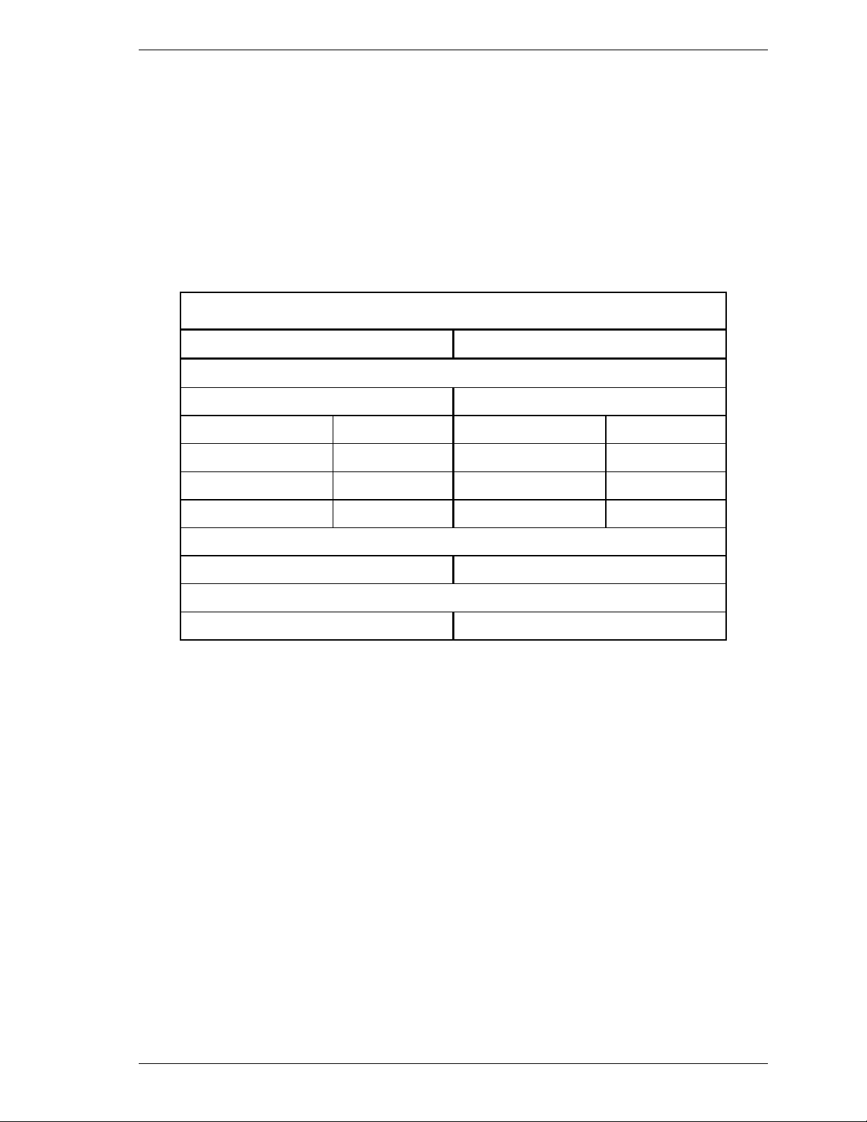
5.2 Logical Interface
5.2.2 Outline of the Shadow Block Register
Each transport layer in the host system and device has a block register, which is
called a Shadow Block Register in the host system, and a Block Register in the
device.
These registers are used when the host system issues a command to the device.
Table 5.3 Shadow Block Register
Command Block registers
Read Write
Data Port
Error Features
Sector Count (exp) Sector Count Sector Count (exp) Sector Count
Sector Number (exp) Sector Number Sector Number (exp) Sector Number
Cylinder Low (exp) Cylinder Low Cylinder Low (exp) Cylinder Low
Cylinder High (exp) Cylinder High Cylinder High (exp) Cylinder High
Device / Head
Status Command
Control Block registers
Alternate Status Device Control
Note: Each of the Sector Count, Sector Number, Cylinder Low, and Cylinder
High fields has a higher-order field used for issuing the Ext command.
The fields are called Sector Count exp, Sector Number exp, Cylinder
Low exp, and Cylinder High exp, respectively. For information on
writing data to these fields, see "Device Control Field."
C141-E262 5-13
Page 92

Interface
5.2.3 Outline of the frame information structure (FIS)
The transport layer converts data written in a Block Register into the FIS, and
sends it to the upper layer.
The FIS, which is generated in the transport layer, is explained below.
5.2.3.1 FIS types
The types of FIS are as follows (Each FIS is referred to as abbreviation in square
brackets in this manual.):
• Register- Host to Device [RegHD]
• Register- Device to Host [RegDH]
• DMA Active – Device to Host [DMA Active]
• DMA Setup – Device to Host or Host to Device (Bidirectional)
[DMA Setup]
• Set Device Bits – Device to Host [SetDB]
• BIST Active – Bidirectional [BIST Active]
• PIO Setup – Device to Host [PIO Setup]
• Data – Host to Device or Device to Host (Bidirectional) [DATA]
5-14 C141-E262
Page 93

5.2 Logical Interface
5.2.3.2 Register - Host to Device
The Register - Host to Device FIS has the following layout:
31 30 29 28 27 26 25 24 23 222120191817161514131211109 8 7 6 5 4 3 2 1 0
0
1
2
3
4
Features Command C R R Reserved (0) FIS Type (27h)
Device LBA High LBA Mid LBA Low
Features (exp) LBA High (exp) LBA Mid (exp) LBA Low (exp)
Control Reserved (0) Sector Count (exp) Sector Count
Reserved (0) Reserved (0) Reserved (0) Reserved (0)
Figure 5.4 Register - Host to Device FIS l ayout
The host system uses the Register - Host to Device FIS when information in the
Register Block is transferred from the host system to the device. This is the
mechanism for issuing the ATA command from the host system to the device.
C - To update the Command field, "1" would be set in this field; and to update
the Device Control field, "0" would be set in the field.
If both C = 1 and SRST = 1 are set, operation is not guaranteed.
C141-E262 5-15
Page 94
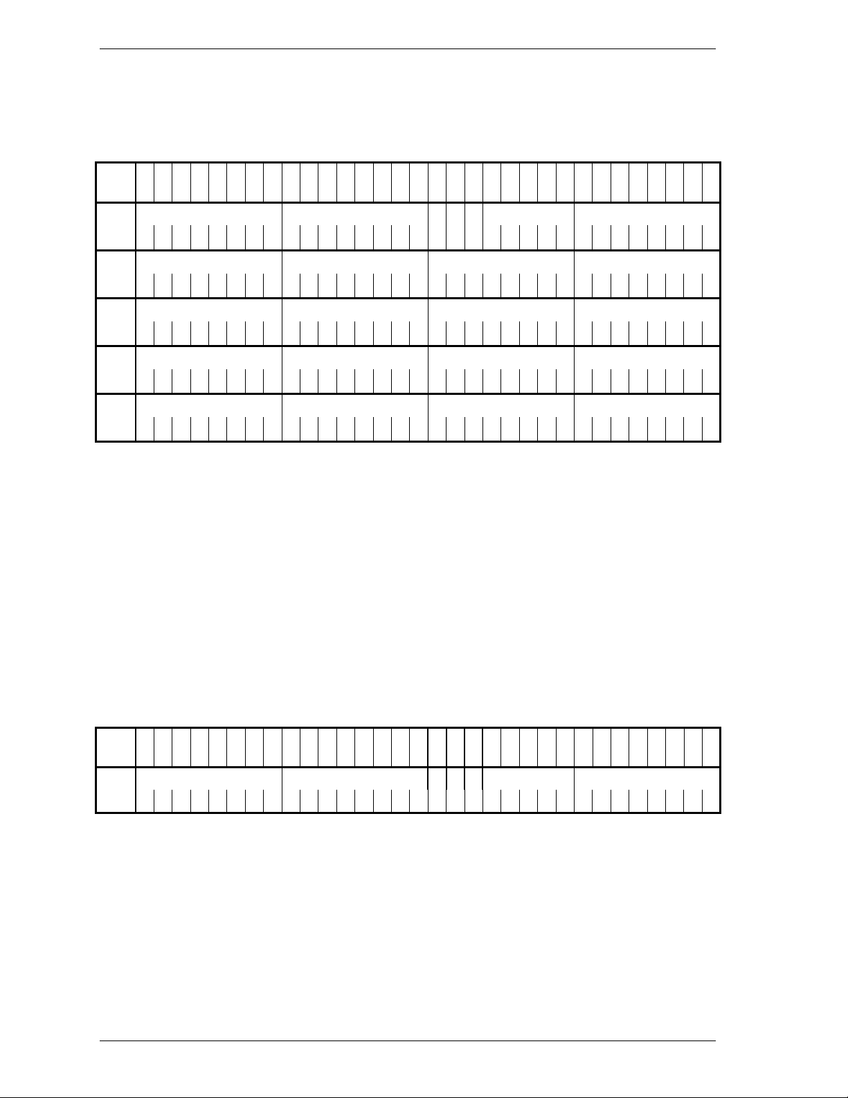
Interface
5.2.3.3 Register - Device to Host
The Register - Device to Host FIS has the following layout:
31 30 29 28 27 26 25 24 23 22 21 20191817161514131211109 8 7 6 5 4 3 2 1 0
0
Error Status R I R Reserved (0) FIS Type (34h)
1
Device LBA High LBA Mid LBA Low
2
Reserved (0) LBA High (exp) LBA Mid (exp) LBA Low (exp) (0)
3
Reserved (0) Reserved (0) Sector Count (exp) Sector Count
4
Reserved (0) Reserved (0) Reserved (0) Reserved (0)
Figure 5.5 Register - Device to Host FIS l ayout
The Register - Device to Host FIS is used when information concerning the Shadow
Register Block in the host adapter is updated. This FIS indicates that the device has
completed a command operation. Furthermore, this is a mechanism for changing
information concerning the Shadow Register Block of the host adapter.
I - If this bit is set, an interrupt request is issued to the host system.
5.2.3.4 DMA Active - Device to Host
The DMA Active - Device to Host FIS has the following layout:
31 30 29 28 27 26 25 24 23 22 21 20191817161514131211109 8 7 6 5 4 3 2 1 0
0
Reserved (0) Reserved (0) R R R Reserved (0) FIS Type (39h)
Figure 5.6 DMA Active - Device to Host FIS layout
The host uses the DMA Active - Device to Host FIS layout. This FIS instructs
the host to continue transferring DMA data from the host to the device.
5-16 C141-E262
Page 95
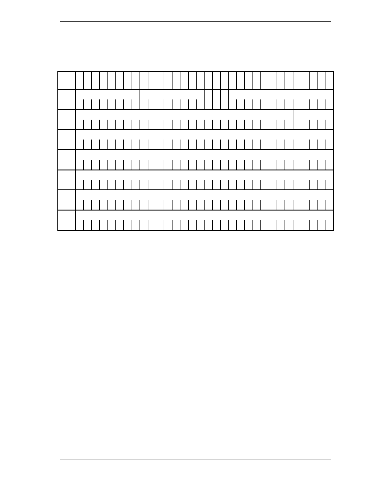
5.2 Logical Interface
5.2.3.5 DMA Setup - Device to Host or Host to Device (Bidirect i onal)
The DMA Setup - Device to Host or Host to Device FIS has the following layout:
31 30 29 28 27 26 25 24 23 2221201918171615141312111098 7 6 5 4 3210
0
Reserved (0) Reserved (0) A I D Reserved (0) FIS Type (41h)
1
0 TAG
2
0
3
Reserved (0)
4
DMA Buffer Offset
5
DMA Transfer Count
6
Reserved (0)
Figure 5.7 DMA Setup - Device to Host or Host t o Device FIS layout
The DMA Setup - Device to Host or Host to Device FIS communicates the start
of a first-party DMA access to the host system. This FIS is used to request the
host system or device to set up the DMA controller before the start of a DMA
data transfer.
A - Auto Active bit. If this bit is cleared ("0" is set for the bit), it indicates that a
DMA Active FIS transfer is required before a Data FIS transfer.
D - Direction bit. If this bit is set ("1" is set for the bit), it indicates that the data
transfer direction is from the device to the host system.
C141-E262 5-17
Page 96

Interface
5.2.3.6 BIST Active - Bidirectional
The BIST Active - Bidirectional FIS has the following layout:
31 30 29 28 27 26 25 24 23 22 21 20191817161514131211109 8 7 6 5 4 3 2 1 0
0
Reserved (0) Pattern definition R R R Reserved (0) FIS Type (58h)
T A S LFPRV
1
Data [31:24] Data [23:16] Data [23:16] Data [7:0]
2
Data [31:24] Data [23:16] Data [23:16] Data [7:0]
Figure 5.8 BIST Active - Bidirectional FIS layout
The BIST Active - Bidirectional FIS is used to set the receiver to Loop Back
mode. This FIS can be sent by either the host system or device.
The following combinations of pattern definitions are supported:
Table 5.4 BIST combinations
T A S L F P V
SC
Reg
Contents
- - - 1 - - 1 09h SATA Phy Analog Loopback Mode
- - - 1 - - - 10h Far End Retimed Loopback Mode
1 1 - - - - -
C0h No ALIGN Transmit_only Mode (Scramble ON)
(*1)
1 1 1 - - - - E0h No ALIGN Transmit_only Mode (Scramble OFF)
1 1 - - - 1 -
1 1 1 - - 1 -
C4h No ALIGN Transmit_only with primitive Mode
(Scramble ON) (*1)
E4h No ALIGN Transmit_only with primitive Mode
(Scramble OFF)
1 - - - - - - 80h ALIGN Transmit_only Mode (Scramble ON) (*1)
1 - 1 - - - - A0h ALIGN Transmit_only Mode (Scramble OFF)
1 - - - - 1 -
1 - 1 - - 1 -
84h ALIGN Transmit_only with primitive Mode
(Scramble ON) (*1)
A4h ALIGN Transmit_only with primitive Mode
(Scramble OFF)
5-18 C141-E262
Page 97

5.2 Logical Interface
5.2.3.7 Data - Host to Device or Device to Host (Bidirectional )
This Data FIS has the following layout:
31 30 29 28 27 26 25 24 23 2221201918171615141312111098 7 6 5 4 3210
0
Reserved (0) Reserved (0) R R R Reserved (0) FIS Type (46h)
...
...
n
Figure 5.9 Data FIS (Bidirecti onal ) layout
The Data FIS is used for data transfers between the host system and device.
5.2.3.8 PIO Setup - Device to Host
0
Error Status R I D Reserved (0) FIS Type (5Fh)
N Dwords of data
(1 to 2048 Dwords)
1
Dev / Head Cyl High Cyl Low Sector Number
2
Reserved (0) Cyl High (exp) Cyl Low (exp) Sector Num (exp) (0)
3
E_Status Reserved (0) Sector Count (exp) Sector Count
4
Reserved (0) Transfer Count
Figure 5.10 PIO Setup - Device to Host FIS layout
The PIO Setup FIS is a device to host FIS, FIS Type 5Fh. The PIO Setup FIS is
used by the device to provide the host adapter with the data transfer count and
DRQ block status during the PIO data phase. This information allows the host
adapter to control PIO data transfers. There are two command structure Response
mappings into a Response FIS in the serial transport.
a) 48-bit command structure PIO Setup mapping
b) 28-bit command structure PIO Setup mapping
C141-E262 5-19
Page 98

Interface
FIS Type - Set to a value of 5Fh. Defines the rest of the FIS fields.
Defines the length of the FIS as five Dwords.
Cyl Low - Holds the contents of the cylinder low register of the
Command Block.
Cyl Low (exp) - Contains the contents of the expanded address field of the
Shadow Register Block.
Cyl High - Holds the contents of the cylinder high register of the
Command Block.
Cyl High (exp) - Contains the contents of the expanded address field of the
Shadow Register Block.
D - Indicates whether host memory is being written or read by
the device.
1 = write (device to host), 0 = read (host to device).
Dev / Head - Holds the contents of the device / head register of the
Command Block.
Dev / Head (exp) - Contains the contents of the expanded address field of the
Shadow Register Block.
E_Status - Contains the new value of the status register of the task file
block for correct synchronization of data transfers to host.
Error - Contains the new value of the Error register of the Command
Block at the conclusion of all subsequent Data to Device frames.
I - Interrupt bit. This bit reflects the interrupt bit line of the device.
R - Reserved (0)
Sector Count - Holds the contents of the sector count register of the
Command Block.
Sector Count (exp) - Contains the contents of the expanded address field of the
Shadow Register Block.
Sector Number - Holds the contents of the sector number register of the
Command Block.
Sector Num (exp) - Contains the contents of the expanded address field of the
Shadow Register Block.
Status - Contains the new value of the status register of the
Command Block at the conclusion of all subsequent PIO
Data to Device frames.
Transfer Count - Holds the number of bytes to be transferred in the
subsequent data FIS.
5-20 C141-E262
Page 99

5.2 Logical Interface
5.2.3.9 Set Device Bits - Device to Host
0
Error R Status Hi R Status Lo R I R Reserved (0) FIS Type (A1h)
1
SActive 31:0
Figure 5.11 Set Device Bits FIS
The Set Device Bits -
Device to Host FIS is used by the device to load Shadow
Command Block bits for which the device has exclusive write
access. These bits are the eight bits of the Error register and six of
the eight bits of the Status register. This FIS does not alter bit 7,
BSY, or bit 3, DRQ, of the Shadow Status register.
FIS Type - Set to a value of A1h. Defines the rest of the FIS fields. Defines the
length of the FIS as two Dwords.
I - Interrupt Bit. This bit signals the host adapter to enter an interrupt
pending state if both the BSY bit and the DRQ bit in the shadow
Status register are zero when the frame is received.
Error - Contains the new value of the Error register of the Shadow
Register Block.
Status-Hi - Contains the new value of bits 6, 5, and 4 of the Status register of
the Shadow Register Block.
Status-Lo - Contains the new value of bits 2,1, and 0 of the Status register of
the Shadow Register Block.
SActive - The SActive field of the Set Device Bits FIS communicates
successful completion notification for each of up to 32 queued
commands. The field is bit-significant and the device sets bit
positions to one for each command tag it is indicating successful
completion notification for. The device may set more than one bit
to one if it is explicitly aggregating successful status returns. The
device shall only indicate completion notification for a command if
it has completed successfully.
C141-E262 5-21
Page 100

Interface
5.2.4 Shadow block registers
(1) Error Field
The Error Field indicates the status of the command executed by the device.
The fields are valid when the ERR bit of the Status field is 1.
This register contains a diagnostic code after power is turned on, the COMRESET
or the EXECUTIVE DEVICE DIAGNOSTIC command is executed.
• [Status at the completion of command execution other than diagnostic command]
Bit 7 Bit 6 Bit 5 Bit 4 Bit 3 Bit 2 Bit 1 Bit 0
X UNC X IDNF/ SFRW SFRR ABRT TK0NF AMNF
X: Unused
- Bit 7: Unused
- Bit 6: Uncorrectable Data Error (UNC). This bit indicates that an
uncorrectable data error has been encountered.
- Bit 5: Unused
- Bit 4: ID Not Found (IDNF). This bit indicates an error except for bad sector,
uncorrectable error and SB not found.
Or, SATA Frame Error Write (SFRW) This bit indicates that a SATA
communication error has been encountered during the write process.
In this case, bit4 and bit2 are set both.
- Bit 3: SATA Frame Error Read (SF RR). This bit indicates that a SATA
communication error has been encountered during the read process.
In this case, bit3 and bit2 are set both.
- Bit 2: Aborted Command (ABRT). This bit indicates that the requested
command was aborted due to a device status error (e.g. Not Ready,
Write Fault) or the command code was invalid.
- Bit 1: Track 0 Not Found (TK0NF). This bit indicates that track 0 was not
found during RECALIBRATE command execution.
- Bit 0: Address Mark Not Found (AMNF). This bit indicates that the SB Not
Found error occurred.
[Diagnostic code]
- X '00': Format Unit is not completed.
- X '01': No Error Detected.
- X '02': HDC Diagnostic Error
- X '03': Data Buffer Diagnostic Error
- X '04': Memory Diagnostic Error
- X '05': Reading the system area is abnormal.
- X '06': Calibration is abnormal.
5-22 C141-E262
 Loading...