

Page 1

Fujitsu Microelectronics (Shanghai) Co., Ltd
Application Note
F²MC-8FX FAMILY
8-BIT MICROCONTROLLER
MB95200H/210H SERIES
MCU-AN-500009-E-10
HOW TO USE DBG PIN
APPLICATION NOTE
Page 2
DBG pin operation V1.0
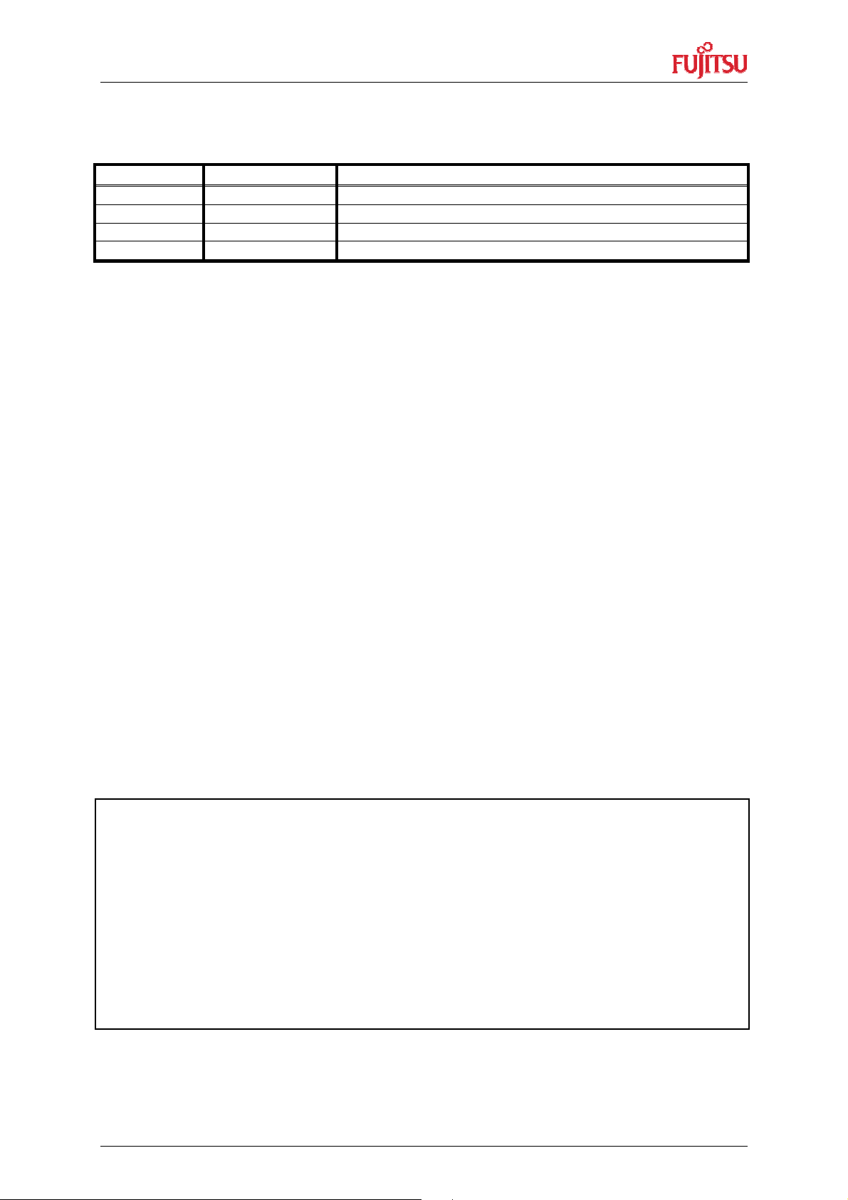
Revision History
Revision History
Date Author Change record
2008-03-18 Raven Peng V1.0 First draft
This document contains 12 pages.
1. The products described in this manual and the specifications thereof may be changed without prior notice.
To obtain up-to-date information and/or specifications, contact your Fujitsu sales representative or Fujitsu
authorized dealer.
2. Fujitsu will not be liable for infringement of copyright, industrial property right, or other rights of a third party
caused by the use of information or drawings described in this manual.
3. The contents of this manual may not be transferred or copied without the express permission of Fujitsu.
4. The products contained in this document are not intended for use with equipments which require extremely
high reliability such as aerospace equipments, undersea repeaters, nuclear control systems or medical
equipment for life support.
5. Some of the products described in this manual may be strategic materials (or special technology) as defined
by the Foreign Exchange and Foreign Trade Control Law. In such cases, the products or portions theory
must not be exported without permission as defined under the law.
© 2008 Fujitsu Microelectronics (Shanghai) Co., Ltd
MCU-AN-500009-E-10 – Page 2
Page 3

Contents
DBG pin operation V1.0
Contents
REVISION HISTORY............................................................................................................ 2
CONTENTS .......................................................................................................................... 3
1 INTRODUCTION.............................................................................................................. 4
2 FUNCTIONS OF DBG PIN............................................................................................... 5
2.1 DBG pin hardware connection (debug mode).......................................................... 5
2.2 Performance in debug mode ................................................................................... 5
2.3 Performance in free-run mode................................................................................. 5
3 HOW TO USE DBG PIN................................................................................................... 6
3.1 Used as 1-line UART pin / P12 pin.......................................................................... 6
3.2 Used as EC0 pin ..................................................................................................... 6
4 PRECAUTIONS IN USING DBG PIN............................................................................... 7
5 SAMPLE CODE ............................................................................................................... 8
MCU-AN-500009-E-10 – Page 3
Page 4

DBG pin operation V1.0
Chapter 1 Introduction
1 Introduction
This application note describes how to use DBG pin. The DBG pin can be used as 1-line
UART communication port in debug mode and can be used as P12/EC0 in free-run mode.
MCU-AN-500009-E-10 – Page 4
Page 5

DBG pin operation V1.0
Chapter 2 Functions of DBG pin
2 Functions of DBG pin
THE FUNCTIONS OF DBG PIN IN DIFFERENT MODES
2.1 DBG pin hardware connection (debug mode)
Figure 2-1 DBG pin hardware connection in debug mode
2.2 Performance in debug mode
If target MCU enter into debug mode, DBG pin performs as 1-line UART pin. To make sure
the real time communication with BGM Adapter, other functions in this pin are disabled.
P12 function is disabled. Any operation for P12 in user code has no effective.
EC0 function is also disabled in this pin. But there is another pin can be used as EC0 pin.
Write “1” to SYSC [EC0SL] can select P04/EC0 pin as external counter clock input. But do
not set EC0 input and HCLK1 input from P04 pin at the same time.
2.3 Performance in free-run mode
If target MCU enter into free-run mode, 1-line UART function is disabled. P12/EC0 functions
can be used by user code. But the DBG pin can not be set as 1-line UART pin by user code.
MCU-AN-500009-E-10 – Page 5
Page 6

DBG pin operation V1.0
T00CR1 =
0
x81
; // enable output, start timer00
.
T00CR1 =
0x81
; // enable output, start timer00
.
Chapter 3 How to Use DBG Pin
3 How to Use DBG Pin
EXAMPLES FOR DBG PIN SETTING IN DIFFERENT MODE
3.1 Used as 1-line UART pin / P12 pin
In Debug mode, DBG pin is used as 1-line UART pin automatically. Then DBG pin keeps
high when UART is in idle status. And in free-run mode, DBG pin is used as P12 according
to default setting. If write user code as follow:
DDR1_D12 = 1; // set P12 as output pin
PDR1_P12 = 0; // pull P12 to low.
After execute these codes in debug mode, the DBG pin still keeps high level. But after run
these codes in free-run mode, the DBG pin pulls to low level.
3.2 Used as EC0 pin
DBG pin can’t be used as EC0 pin in debug mode. To realize the external clock input for the
8/16 compound timer, EC0 pin can be changed to P04 pin in debug mode.
SYSC = 0xEB; // set P04 as EC0 pin, disable HCLK1
T00CR0 = 0x71; // interval timer, external clock source.
TMCR0 = 0x43; // 8bit mode, output timer00.
T00DR = 0x08; // set counter.
The upper sample code sets P04 as EC0 pin, and sets Timer00 in continuous interval timer
mode. Input a clock signal to P04 pin; execute these codes in debug mode; check the T00
pin; you can see the output clock is the input clock divided by 8.
SYSC = 0xE3; // set P12 as EC0 pin, disable HCLK1
T00CR0 = 0x71; // interval timer, external clock source.
TMCR0 = 0x43; // 8bit mode, output timer00.
T00DR = 0x08; // set counter.
The upper sample code sets P12 as EC0 pin, and sets Timer00 in continuous interval timer
mode. Input a clock signal to P12 pin; run these codes in free-run mode, check the T00 pin,
you can see the output clock is the input clock divided by 8.
MCU-AN-500009-E-10 – Page 6
Page 7

DBG pin operation V1.0
Chapter 4 Precautions in using DBG pin
4 Precautions in using DBG pin
1. The peripheral circuit connected to DBG pin shouldn’t influence the 1-line UART
communication if using BGM Adapter to do debug. Please refer to figure 2-1 when design
user board.
2. It is recommended that set P12 as input pin or output low in user code when doing debug.
Do not set P12 to output high. Because if set P12 output high, DBG pin will output high when
target MCU runs in free-run mode. And if target board is connected with BGM adapter in this
condition, a large current will run through DBG pin when BGM adapter transports bit “0” with
1-line UART pin.
MCU-AN-500009-E-10 – Page 7
Page 8

DBG pin operation V1.0
Chapter 5 Sample code
5 Sample code
Start.asm
//==================================================================
// F2MC-8L Family SOFTUNE C Compiler sample startup routine,
//ALL RIGHTS RESERVED, COPYRIGHT (C) FUJITSU LIMITED 1986
// LICENSED MATERIAL - PROGRAM PROPERTY OF FUJITSU LIMITED
//==================================================================
//Sample code for initialization
//-----------------------------------------------------------------------
.PROGRAM start
.TITLE start
// Settings
#set OFF 0
#set ON 1
# set STACKSIZE 64 // Stack size
//Clock Mode Selection
# set SUB 0 //Sub clock mode
# set MAIN 2 // Main clock mode
//DIV Clock Selection (Machine clock division ratio)
# set CLK_0 0 // Original oscillator div 1
# set CLK_4 1 // Original oscillator div 4
# set CLK_8 2 //Original oscillator div 8
# set CLK_16 3 //Original oscillator div 16
// external declaration of symbols
.IMPORT _main
//definition to stack area
.RES.B STACKSIZE
STACK_TOP:
.SECTION STACK, STACK, ALIGN=1
.EXPORT __start
.RES.B 2
//========= ===============================================
// Start-Up Code
//=======================================================
// ___ _____ __ ___ _____
// / | / \ | \ |
// \___ | | | |___/ |
// \ | |----| | \ |
// ___/ | | | | \ |
MCU-AN-500009-E-10 – Page 8
Page 9

DBG pin operation V1.0
Chapter 5 Sample code
//Begin of actual code section
//========================================================
//The Mode Byte is defined at the beginning of the start.asm
.DATA.B 0
.DATA.W __start
; code area
.SECTION CODE, CODE, ALIGN=1
__start:
; set stack pointer
MOVW SP , A
// Set Register bank Pointer 0 / set Direct bank Pointer 0 (0x80..0xFF)
MOVW A , #0x00BF // RP=0, DP=0, I=0
ANDW A
MOVW PS , A
// Set ILM to the lowest level(3)
MOVW A , PS
MOVW A , #0x0030
.SECTION RESVECT, CONST, LOCATE=H'FFFD
MOVW A , #STACK_TOP
MOVW A , PS
ORW A
MOVW PS , A
MOV A , 0X0FE4 // READ CRTH
AND A , #0X9F //CLEAR CRTH[6:5]
OR A , #0X60 // 10MHz, 0X00: 1MHz
//0X20: 12.5MHz
// 0X40: 10MHz 0X60: 8MHz
MOV 0X0FE4 , A // WRITE SYSC
// call main routine
CALL _main
end: JMP end
.END __start
MCU-AN-500009-E-10 – Page 9
Page 10

DBG pin operation V1.0
Chapter 5 Sample code
vector.c
/******************************vector.c*********************************/
THIS SAMPLE CODE IS PROVIDED AS IS AND IS SUBJECT TO ALTERATIONS. FUJITSU
MICROELECTRONICS ACCEPTS NO RESPONSIBILITY OR LIABILITY FOR ANY ERRORS OR
ELIGIBILITY FOR ANY PURPOSES.
/********************************************************************/
// VECTORS.C Interrupt level (priority) setting
- Interrupt vector definition
#include "mb95200.h"
void InitIrqLevels(void)
{ ILR0 = 0xEF; // IRQ0: external interrupt ch4 --> 01
// IRQ1: external interrupt ch5 --> 01
// IRQ2: external interrupt ch2 | ch6 --> 01
// IRQ3: external interrupt ch3 | ch7 --> 01
ILR1 = 0xFF; // IRQ4: UART/SIO ch0
// IRQ5: 8/16-bit timer ch0 (lower)
// IRQ6: 8/16-bit timer ch0 (upper)
// IRQ7: LIN-UART (reception)
ILR2 = 0xFF; // IRQ8: LIN-UART (transmission)
// IRQ9: 8/16-bit PPG ch1 (lower) | UART/SIO ch1
// IRQ10: 8/16-bit PPG ch1 (upper) | I2C ch1
// IRQ11: 16-bit reload timer ch0
ILR3 = 0xFF; // IRQ12: 8/16-bit PPG ch0 (upper)
// IRQ13: 8/16-bit PPG ch0 (lower)
// IRQ14: 8/16-bit timer ch1 (upper)
// IRQ15: 16-bit PPG ch0 + ch2
ILR4 = 0xFF; // IRQ16: 16-bit reload timer ch1 | I2C ch0
// IRQ17: 16-bit PPG ch1
// IRQ18: 10-biat A/D-converter --> 01
// IRQ19: Timebase timer
ILR5 = 0xFF; // IRQ20: Watch timer / counter
// IRQ21: external interrupt ch 8-11
// IRQ22: 8/16-bit timer ch1 (lower) | external
interrupt ch 12-15
// IRQ23: Flash | Custom ch1
}
// Prototypes
//================================================================
//Add your own prototypes here. Each vector definition needs is prototype.
Either do it here or include a header file containing them.
MCU-AN-500009-E-10 – Page 10
Page 11

DBG pin operation V1.0
Chapter 5 Sample code
//===================================================================
//extern unsigned int delay_timer;
__interrupt void DefaultIRQHandler (void);
// Vector definition
// Use following statements to define vectors.
// All resource related vectors are predefined.
// Remaining software interrupts can be added hereas well.
#pragma intvect DefaultIRQHandler 0 //IRQ0: external interrupt ch4
#pragma intvect DefaultIRQHandler 1 //IRQ1: external interrupt ch5
#pragma intvect DefaultIRQHandler 2 //IRQ2: external interrupt ch2 | ch6
#pragma intvect DefaultIRQHandler 3 //IRQ3: external interrupt ch3 | ch7
#pragma intvect DefaultIRQHandler 5 //IRQ5: 8/16-bit timer ch0 (lower)
#pragma intvect DefaultIRQHandler 6 //IRQ6: 8/16-bit timer ch0 (upper)
#pragma intvect DefaultIRQHandler 7 //IRQ7: LIN-UART (reception)
#pragma intvect DefaultIRQHandler 8 //IRQ8: LIN-UART (transmission)
#pragma intvect DefaultIRQHandler 14 //IRQ14: 8/16-bit timer ch1 (upper)
#pragma intvect DefaultIRQHandler 18 //IRQ18: 10-biat A/D-converter
#pragma intvect DefaultIRQHandler 19 //IRQ19: Timebase timer
#pragma intvect DefaultIRQHandler 20 //IRQ20: Watch timer / counter
#pragma intvect DefaultIRQHandler 22 //IRQ22: 8/16-bit timer ch1 (lower) |
// external interrupt ch 12-15
#pragma intvect DefaultIRQHandler 23 //IRQ23: Flash | Custom ch1
__interrupt
void DefaultIRQHandler (void)
{
__DI(); // disable interrupts
While(1)
__wait_nop(); // halt system
}
Main.c
//=====================================================================
//following code created for DBG pin usage test
#define DEBUGMODE
//set DBG pin as P12 output
void gpio_setting(void)
{
DDR1_P12 = 1; /* set P12 as output pin */
PDR1_P12 = 0; /* pull P12 to low. */
AIDRL_P04 = 1; /* port input enable */
}
MCU-AN-500009-E-10 – Page 11
Page 12

DBG pin operation V1.0
Chapter 5 Sample code
//set DBG pin as EC0 pin
void p12_as_ec0(void)
{
SYSC = 0xE3; // set P12 as EC0 pin, disable HCLK1
T00CR0 = 0x71; // interval timer, external clock source.
TMCR0 = 0x43; // 8bit mode, output timer00.
T00DR = 0x08; // set counter.
T00CR1 = 0x81; // enable output, start timer00.
}
//change EC0 pin to P04
void p04_as_ec0(void)
{
SYSC = 0xEB; // set P04 as EC0 pin, disable HCLK1
T00CR0 = 0x71; // interval timer, external clock source.
TMCR0 = 0x43; // 8bit mode, output timer00.
T00DR = 0x08; // set counter.
T00CR1 = 0x81; // enable output, start timer00.
}
//main function
void main(void)
{
gpio_setting(); //pull low P12 pin
...
#ifdef DEBUGMODE
P04_as_ec0(); //set P04 as EC0 pin in debug mode
#else
P12_as_ec0(); //set P12 as EC0 pin in free run mode
#endif
}
MCU-AN-500009-E-10 – Page 12
 Loading...