

Page 1

AN07-00180-3E
FR Family FR60 Lite
32-BIT MICROCONTROLLER
MB91F267N
bits pot red
CAN-Motor board
User’s Manual
Page 2

Date
Revision
August 01, 2008
Revision 1.0: Initial release
September 17, 2008
Revision 1.1
On p.12, type corrected. Correct: NL565050T-103J, Incorrect: L565050T-103J
October 22, 2008
Revision 1.2
On p.13, a download web page is changed.
On p.20, "1.1.1 Downloading the software" is added.
On p.25, p.30, p.36 and p.43,
Description is corrected about the extracting file.
The file path is added.
(left blank)
Revision History
AN07-00180-3E
- 2 -
Page 3

AN07-00180-3E
Note
- The contents of this document are subject to change without notice. Customers are advised to consult
with FUJITSU sales representatives before ordering.
- The information, such as descriptions of function and application circuit examples, in this document are
presented solely for the purpose of reference to show examples of operations and uses of Fujitsu
semiconductor device; Fujitsu does not warrant proper operation of the device with respect to use based
on such information. When you develop equipment incorporating the device based on such information,
you must assume any responsibility arising out of such use of the information. Fujitsu assumes no
liability for any damages whatsoever arising out of the use of the information.
- Any information in this document, including descriptions of function and schematic diagrams, shall not
be construed as license of the use or exercise of any intellectual property right, such as patent right or
copyright, or any other right of Fujitsu or any third party or does Fujitsu warrant non-infringement of any
third-party’s intellectual property right or other right by using such information. Fujitsu assumes no
liability for any infringement of the intellectual property rights or other rights of third parties which
would result from the use of information contained herein.
- The products described in this document are designed, developed and manufactured as contemplated for
general use, including without limitation, ordinary industrial use, general office use, personal use, and
household use, but are not designed, developed and manufactured as contemplated (1) for use
accompanying fatal risks or dangers that, unless extremely high safety is secured, could have a serious
effect to the public, and could lead directly to death, personal injury, severe physical damage or other loss
(i.e., nuclear reaction control in nuclear facility, aircraft flight control, air traffic control, mass transport
control, medical life support system, missile launch control in weapon system), or (2) for use requiring
extremely high reliability (i.e., submersible repeater and artificial satellite).
Please note that Fujitsu will not be liable against you and/or any third party for any claims or damages
arising in connection with above-mentioned uses of the products.
- Any semiconductor devices have an inherent chance of failure. You must protect against injury, fire,
damage or loss from such failures by incorporating safety design measures into your facility and
equipment such as redundancy, fire protection, and prevention of over-current levels and other abnormal
operating conditions.
- If any products described in this document represent goods or technologies subject to certain restrictions
on export under the Foreign Exchange and Foreign Trade Law of Japan, the prior authorization by
Japanese government will be required for export of those products from Japan.
- The company names and brand names herein are the trademarks or registered trademarks of their
respective owners.
Copyright© 2008 FUJITSU MICROELECTRONICS LIMITED all rights reserved
- 3 -
Page 4

AN07-00180-3E
Table of Contents
Revision History ......................................................................................................................... 2
Note .......................................................................................................................................... 3
Introduction .............................................................................................................................. 10
Contact .................................................................................................................................... 11
Suppliers of the parts/materials .................................................................................................... 12
1 Setting up the starter kit ...................................................................................................... 13
1.1 Setting up the PC ..................................................................................................... 19
1.1.1 Downloading the software ........................................................................................ 20
1.1.2 Installing a USB driver ............................................................................................ 20
1.1.3 Installing the integrated development environment SOFTUNE (bits pot dedicated version) ............ 25
1.1.4 Installing PC Writer (bits pot red dedicated version) ..................................................... 30
1.1.5 Configuring the evaluation board and connecting it to the PC ........................................ 33
2 Running the program .......................................................................................................... 35
2.1 Executing in single chip mode................................................................................... 36
2.1.1 Building a project .................................................................................................... 36
2.1.2 Writing the program into the microcontroller............................................................... 38
2.2 Debugging by using Monitor Debugger ..................................................................... 43
2.2.1 Writing Monitor Debugger into the microcontroller ..................................................... 43
2.2.2 Activating SOFTUNE and configuring the debug settings ............................................. 48
2.2.3 Writing the program into the microcontroller............................................................... 55
2.2.4 Loading the target file ................................................................ .............................. 57
2.2.5 Running the debugger .............................................................................................. 58
2.2.6 Notes on Monitor Debugger...................................................................................... 59
3 Operation of the sample program .......................................................................................... 60
3.1 bits pot red single-unit operation ............................................................................... 61
3.2 CAN communication operation (CAN communication operation with the bits pot white) .......... 63
4 Try to rotate the BLDC motor .............................................................................................. 65
4.1 What is the BLDC motor? ......................................................................................... 65
4.2 How does the BLDC motor rotate? ........................................................................... 66
4.3 BLDC motor rotation control by the microcontroller ................................................... 68
4.4 Understanding and running the program for the BLDC motor operation ..................... 75
4.5 Handling controls of the BLDC motor ........................................................................ 78
5 Try to use CAN communication ........................................................................................... 82
5.1 What is CAN? ........................................................................................................... 82
- 4 -
Page 5

AN07-00180-3E
5.2 CAN specifications ................................................................................................... 84
5.2.1 CAN frame configurations ................................................................................. 84
5.2.2 Arbitration ............................................................................................................. 88
5.2.3 Error management ................................................................................................... 90
5.3 CAN communication by using the microcontroller ..................................................... 92
5.4 Understanding and running the program for CAN communication ............................. 95
5.4.1 CAN communication configuration ........................................................................... 95
5.4.2 Sample program sequence ........................................................................................ 99
6 Appendix ........................................................................................................................ 104
6.1 Sample program folder/file configuration ................................................................. 104
- 5 -
Page 6

AN07-00180-3E
List of Figures
Figure 1-1 External board view ......................................................................................... 14
Figure 1-2 System connection diagram ............................................................................ 16
Figure 1-3 Downloading the USB driver ................................................................................ 20
Figure 1-4 Installing FT232R USB UART ............................................................................. 21
Figure 1-5 Selecting the search locations................................................................................ 22
Figure 1-6 Completing the USB Serial Converter installation.................................................... 22
Figure 1-7 Installing USB Serial Port .................................................................................... 23
Figure 1-8 Selecting the search locations................................................................................ 23
Figure 1-9 Completing the USB Serial Port installation ............................................................ 24
Figure 1-10 SOFTUNE setup confirmation ............................................................................ 25
Figure 1-11 Starting SOFTUNE setup ................................................................................... 25
Figure 1-12 Caution on SOFTUNE setup ............................................................................... 26
Figure 1-13 SOFTUNE setup/License agreement .................................................................... 26
Figure 1-14 SOFTUNE setup/Version information .................................................................. 27
Figure 1-15 SOFTUNE setup/Selecting the destination of installation ........................................ 27
Figure 1-16 SOFTUNE setup/Selecting the components........................................................... 28
Figure 1-17 SOFTUNE setup/Confirming the installation settings ............................................. 28
Figure 1-18 SOFTUNE setup/Completion .............................................................................. 29
Figure 1-19 PC Writer/Installation dialog ............................................................................... 30
Figure 1-20 PC Writer/Setup type ................................................................ ......................... 31
Figure 1-21 PC Writer/Ready to install .................................................................................. 31
Figure 1-22 Completing the PC Writer installation .................................................................. 32
Figure 1-23 MODE selection................................................................................................ 33
Figure 1-24 Connection between the PC and the board............................................................. 34
Figure 2-1 Opening a workspace ........................................................................................... 36
Figure 2-2 Selecting a workspace .......................................................................................... 37
Figure 2-3 Building a project ................................................................................................ 37
Figure 2-4 Completing the build ........................................................................................... 38
Figure 2-5 Opening the file to write....................................................................................... 38
Figure 2-6 Selecting the file to write ...................................................................................... 39
Figure 2-7 Select the COM port to be used for the writing ........................................................ 40
Figure 2-8 Checking the COM port ....................................................................................... 41
Figure 2-9 Writing the program ............................................................................................ 42
Figure 2-10 Completing the program writing .......................................................................... 42
- 6 -
Page 7

AN07-00180-3E
Figure 2-11 Opening the file to write ..................................................................................... 43
Figure 2-12 Selecting the file to write .................................................................................... 44
Figure 2-13 Select the COM port to be used for the writing ...................................................... 45
Figure 2-14 Checking the COM port ..................................................................................... 46
Figure 2-15 Writing the program ........................................................................................... 47
Figure 2-16 Completing the program writing .......................................................................... 47
Figure 2-17 Opening a workspace ......................................................................................... 48
Figure 2-18 Selecting a workspace ........................................................................................ 49
Figure 2-19 Building a project .............................................................................................. 49
Figure 2-20 Completing the build ......................................................................................... 50
Figure 2-21 Changing the debug settings ......................................................................... 50
Figure 2-22 Starting the debug setting wizard ......................................................................... 51
Figure 2-23 Selecting the debugger type ................................................................................ 51
Figure 2-24 Selecting the device type .................................................................................... 52
Figure 2-25 Specifying a batch file ........................................................................................ 52
Figure 2-26 Configuring the target file settings ....................................................................... 53
Figure 2-27 Setting setup file selection .................................................................................. 53
Figure 2-28 Completing the setup wizard ............................................................................... 54
Figure 2-29 Start debugging ................................................................................................. 54
Figure 2-30 Showing the commands window.......................................................................... 55
Figure 2-31 Inputting commands ................................ .......................................................... 56
Figure 2-32 Completing the program writing .......................................................................... 56
Figure 2-33 Loading the target file ........................................................................................ 57
Figure 2-34 Setting break points ........................................................................................... 58
Figure 2-35 Running the program ......................................................................................... 58
Figure 2-36 Stopping the program ......................................................................................... 59
Figure 3-1 Single-unit operation/Controls and mechanicals ...................................................... 61
Figure 3-2 CAN communication operation/Controls and mechanicals ........................................ 63
Figure 4-1 DC motor/BLDC motor configuration examples ...................................................... 65
Figure 4-2 Names of the respective elements .......................................................................... 66
Figure 4-3 120° conduction method time chart .................................................................. 67
Figure 4-4 Motor driver circuit ........................................................................................... 68
Figure 4-5 Timer control registers ......................................................................................... 69
Figure 4-6 Output compare registers ...................................................................................... 71
Figure 4-7 Operation of the free-run timer ................................................................ ......... 73
Figure 4-8 U-High output to output comparisons ............................................................... 74
- 7 -
Page 8

AN07-00180-3E
Figure 4-9 Motor operation flowchart .................................................................................... 75
Figure 4-10 Operation mode settings ..................................................................................... 76
Figure 4-11 Main function ................................................................................................... 76
Figure 4-12 SW2 interrupt ................................................................................................... 77
Figure 4-13 Free-run timer interrupt ................................................................ ...................... 77
Figure 4-14 Motor controls flowchart................................................................................. 78
Figure 4-15 Rotation speed control........................................................................................ 79
Figure 4-16 Brake control .................................................................................................... 80
Figure 4-17 Rotation direction control ................................................................................... 81
Figure 5-1 Example of on-board CAN application ................................................................ ... 82
Figure 5-2 CAN bus signal levels.......................................................................................... 83
Figure 5-3 CAN frame configurations ................................................................................... 85
Figure 5-4 Operation of the arbitration ................................................................................... 88
Figure 5-5 Example of arbitration among nodes................................................................ 89
Figure 5-6 CAN status transition ........................................................................................... 91
Figure 5-7 CAN circuit ........................................................................................................ 92
Figure 5-8 Entire CAN communication control register............................................................ 93
Figure 5-9 CAN communication flowchart ......................................................................... 99
Figure 5-10 Operation mode settings ................................................................................... 100
Figure 5-11 Main function ................................................................................................. 100
Figure 5-12 CAN timer interrupt control .............................................................................. 101
Figure 5-13 Motor rotation information transmit ................................................................... 102
Figure 5-14 Temperature sensor information transmit ............................................................ 102
Figure 5-15 CAN receive processing ................................................................................... 103
- 8 -
Page 9

AN07-00180-3E
List of Tables
Table 1-1 Component list.................................................................................................... 13
Table 1-2 Description of the respective board parts .................................................................. 15
Table 1-3 MB91F267N pin assignment .................................................................................. 17
Table 3-1 Single-unit operation/Descriptions of the controls and mechanicals ............................. 62
Table 3-2 CAN communication operation/Descriptions of the controls and mechanicals ............... 64
Table 4-1 Microcontroller pin/Motor driver circuit connections ................................................ 69
Table 4-2 Functions employed by the motor driving macro ....................................................... 69
Table 4-3 Description of the timer control registers and setting values ........................................ 70
Table 4-4 Description of the output compare registers and setting values .................................... 72
Table 4-5 Correspondence between the output compare values and the switchings .......... 73
Table 5-1 Description of the error types ................................................................................. 90
Table 5-2 Description of the entire CAN communication control registers and setting values......... 94
Table 5-3 CAN communication conditions of the sample program ............................................. 95
Table 5-4 CAN message IDs in the sample program ................................................................ 96
Table 6-1 Sample program folder/file configuration ............................................................... 104
- 9 -
Page 10

AN07-00180-3E
Introduction
Thank you very much for purchasing the bits pot red (referred to as this starter kit or the starter kit
hereafter).
This starter kit is a beginner’s kit intended for those who wish to start learning microcontrollers and
on-board network processors. The kit is designed so that the beginners who ask “What is a
microcontroller?”, “How does it work?” and “How does it control a network?” can easily learn what it is.
The kit includes flash microcontroller development tools, so if you have slight understanding about the C
language, you can rewrite a program to let the microcontroller perform in various ways. Even if you do
not know of programming, you may be able to enjoy learning a microcontroller with a study-aid book
about the C language.
This starter kit can also serve as an introductory training tool for electronic circuit practice or future
embedded software development in a class of a college or high school of technology or training for
freshman engineers of a manufacturer.
- 10 -
Page 11

Contact
For inquiries about this starter kit, contact the following address.
Zip code: 105-8420 2-5-3 Nishi-Shinbashi, Minatoku, Tokyo
E-mail: pd-bitspot@tsuzuki-densan.co.jp
bits pot URL: http://www.tsuzuki-densan.co.jp/bitspot/
AN07-00180-3E
- 11 -
Page 12

Suppliers of the parts/materials
Capacitors 22 pF : GCM1552C1H220JZ02
0.1 μF : GCM188R11E104KA42
1 μF : GCM21BR11E105KA42
10 μF : GCM32ER71E106KA42
Ceramic oscillator : CSTCR4M00G15C
NTC Thermistors : NTCG164BH103JT1
AN07-00180-3E
Ferrite Beads : MPZ2012S300AT
Common Mode Filters : ZJYS81R5-2P24T-G01
Inductors : NL565050T-103J
- 12 -
Page 13
AN07-00180-3E
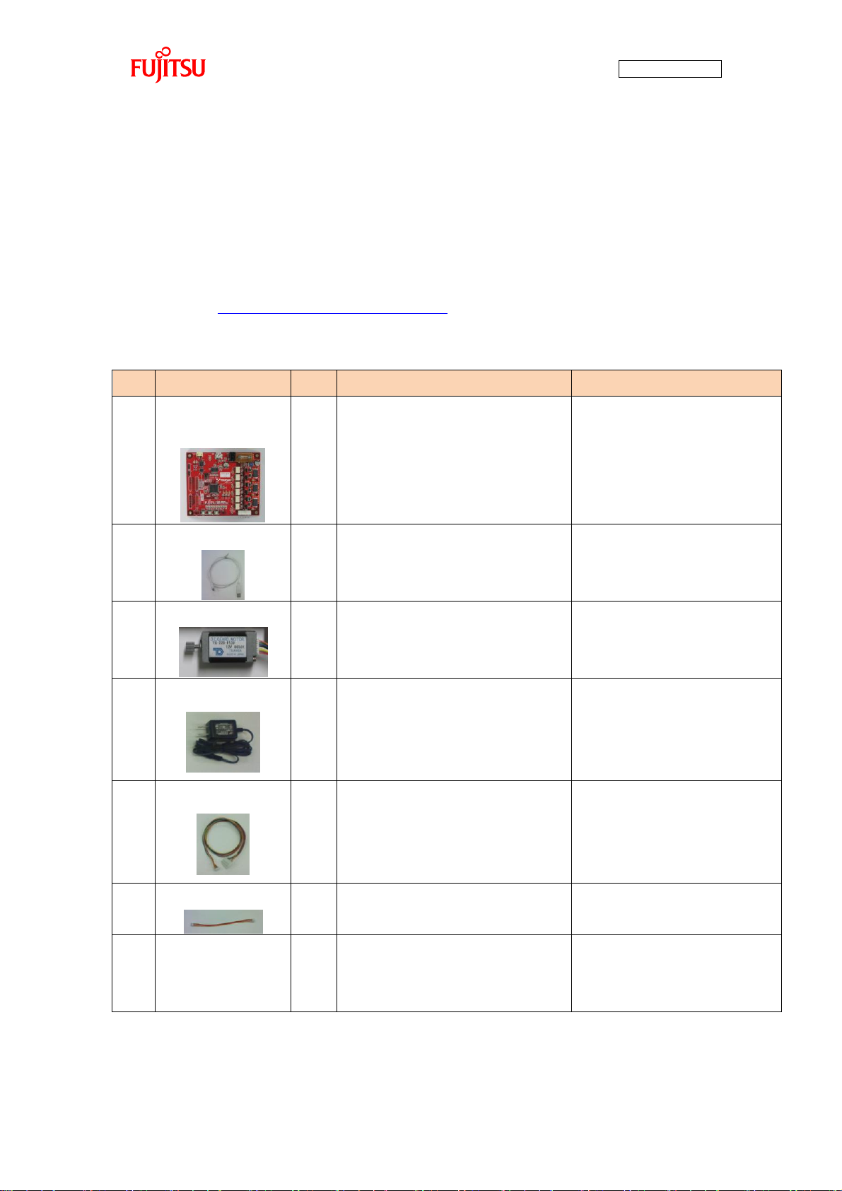
No.
Article
Qty.
Specifications
Remarks
1
bits pot red
CAN motor board
1
Microcontroller made by Fujitsu
FR Family FR60 Lite, MB91F267N
mounted
See Figure 1-1
2
USB cable
1
USB (A to miniB)
Accessory
3
BLDC Motor
1
Tsukasa Electronic TG-22D-F539,
12 V
Accessory
4
AC adapter
1
12 V, 1 A
Accessory
Be sure to use the adapter
included in the kit
5
Motor cable
1
8-pin cable
Accessory
6
CAN cable
1
3-pin cable
Accessory
7
PC 1 On which Windows XP normally
runs and USB2.0 ports are
supported
Prepare the PC by yourself.
1 Setting up the starter kit
Before using this starter kit, be sure to check the components listed in Table 1-1 are fully supplied.
Before connecting the bits pot red CAN-Motor board (referred to as the board hereafter), you need to
install software in your PC. You can download the software required for the starter kit from the following
web site.
bits pot URL: http://www.tsuzuki-densan.co.jp/bitspot/
Table 1-1 Component list
- 13 -
Page 14
AN07-00180-3E
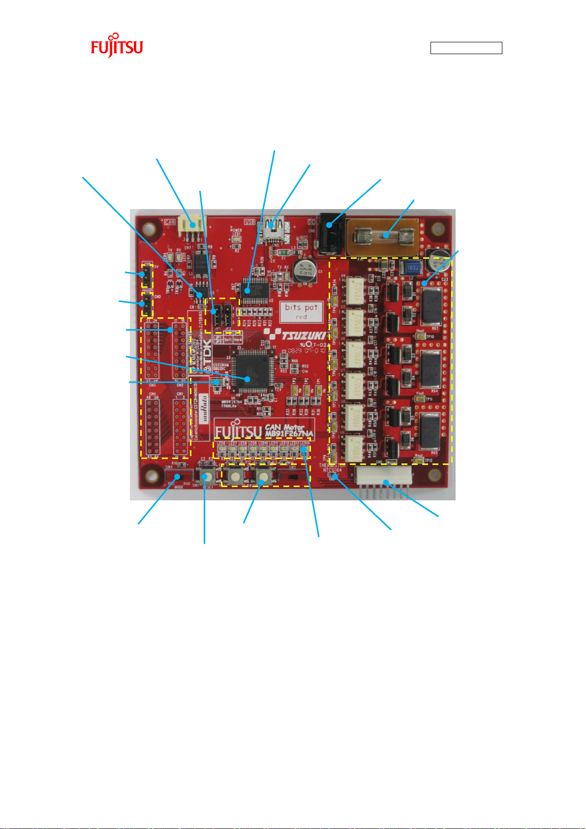
(2) Target device oscillator
(1) Target device
(16) Extension pins
(3) CAN transceiver
(4) CAN connector
(5) USB to UART converter
(6) USB connector
(9) DC jack
(15) Fuse
(7) Motor driver circuit
(8) Motor connector
(14) Temperature sensor
(13) LED lamps
(12) Test SW
(11) Reset SW
(10) Mode SW
(19) Extension GND
(18) Extension power
(17) Jumper pin
Figure 1-1 External board view
- 14 -
Page 15

AN07-00180-3E
No.
Name
Function
Description
(1)
Target device
MB91F267N
Main microcontroller (MB91F267N).
(2)
Target device oscillator
CSTCR4M00G15C
Ceralock made by Murata Manufacturing
Oscillator for the main microcontroller.
(3)
CAN transceiver
MAX3058ASA+
Transceiver IC for CAN communication.
(4)
CAN connector
3-pin connector
Connector for CAN communication.
Connect this connector to the CAN connector on the
bits pot white.
(5)
USB to UART converter
FT232RL
IC for conversion between UART and USB.
(6)
USB connector
miniB
USB connector for connection with the PC to
write/debug a program.
(7)
Motor driver circuit
3-phase motor driver
circuit
Driver circuit for 3-phase motor operation by the main
microcontroller.
(8)
Motor connector
8 pins
Connector for connection with the 3-phase motor
included in the kit.
(9)
DC jack
-
Power connector for the operation of the motor.
(10)
Mode SW
Slide switch
Switch for selection of operation mode of the board.
(11)
Reset SW
Push switch
Switch to reset the board.
(12)
Test switches
Push switch x 2
Slide switch x 1
Connected to the general-purpose I/O port.
The sample program uses this switch for motor rotation.
(13)
LED lamps
LED (green) x 6
LED (red) x 3
General-purpose LED lamps.
(14)
Temperature sensor
NTCG164BH103
NTC thermistor made by TDK
Temperature sensor connected to the A/D converter.
(15)
Fuse
0217001P
Fuse for the 12-V power supply.
(16)
Extension pins
-
Extension pins of the main microcontroller.
For details, see the circuit diagram.
(17)
Jumper pins (JP1, JP2)
-
Jumper pins for USB-UART conversion setting.
UART communication handshake setting.
1-2: Handshake by software.
2-3: Handshake by hardware.
The default setting is 2-3 (common to JP1/JP2).
“Table 1-2 Description of the respective board parts” provides descriptions of the respective board parts.
Table 1-2 Description of the respective board parts
- 15 -
Page 16
(18)
Extension power (5V)
-
Extension 5-V power terminal.
(19)
Extension GND
-
Extension GND terminal.
AC adapter (accessory)
* Prepare the PC by yourself.
BLDC motor (accessory)
Use the AC adapter included in the
kit for the connection. (The motor
power is supplied from the AC
adapter.)
Use the USB cable included in the kit for
the connection. (The power is supplied
from the USB bus power.)
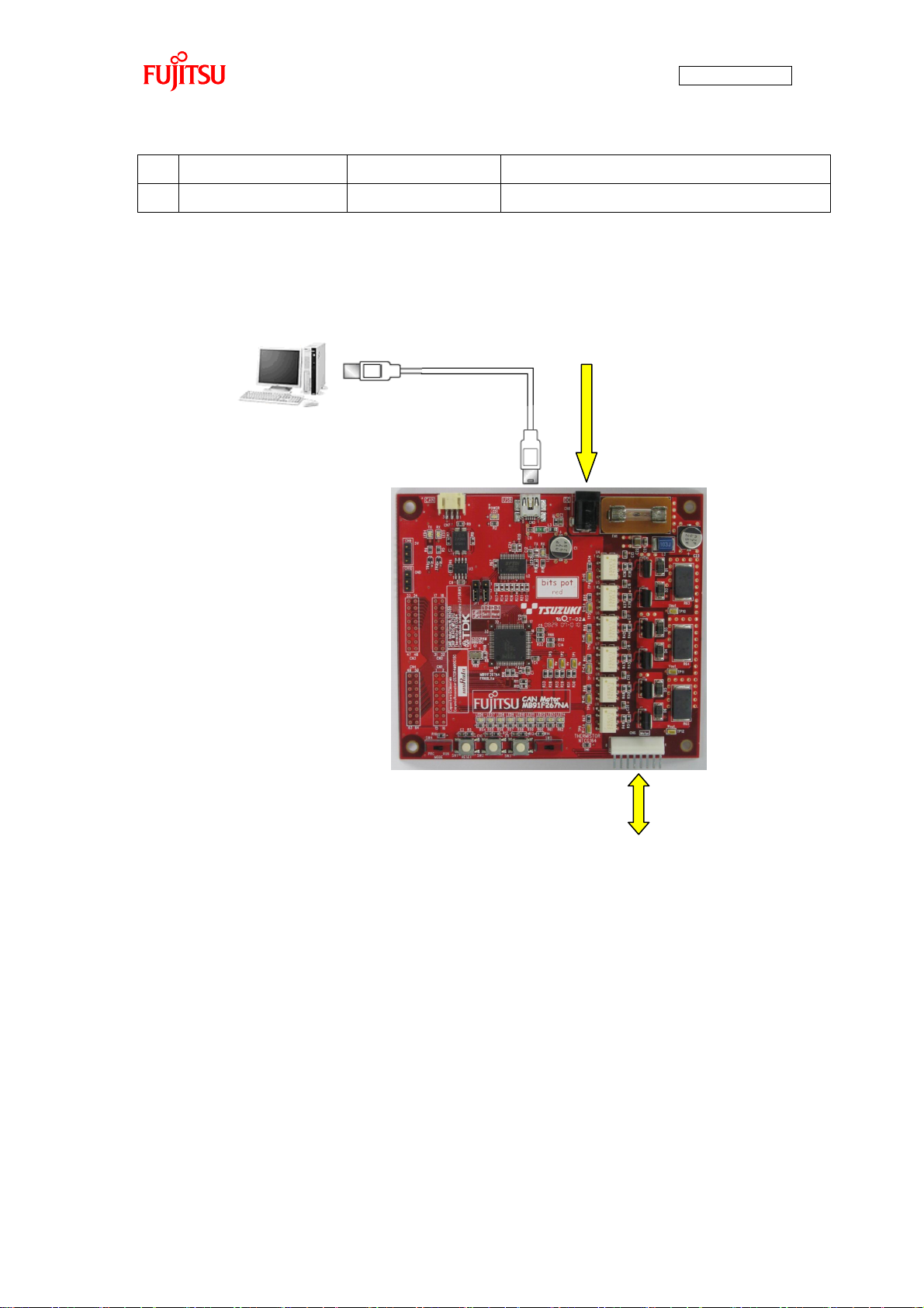
“Figure 1-2 System connection diagram” shows the connection of the system.
AN07-00180-3E
Figure 1-2 System connection diagram
Connect the PC with the board by using the USB cable included in the kit.
The power is supplied to the board from the USB bus power.
Directly connect the USB port to that on the PC. Do not make the connection via a USB hub.
- 16 -
Page 17

AN07-00180-3E
Pin No.
Description
Connected to:
Remarks
1
AVss
GND
2 ACC
GND
3 AN0/P50
Motor driver circuit
4 AN1/P51
Motor driver circuit
5 AN2/P52
Motor driver circuit
6 AN3/P53
- 7
AN4/P54
LED6
L output = On
8
AN5/P55
LED7
L output = On
9
AN6/P56
LED8
L output = On
10
AN7/P57
LED9
L output = On
11
AN8/P44
LED10
L output = On
12
AN9/P45
LED11
L output = On
13
AN10/P46
Thermistor
14
NMI
5 V 15 C GND
16
Vss
GND
17
Vcc
5 V 18
INT4/PPG1/P00
LED12
19
PPG2/P01
LED13
20
INT5/PPG3/P02
LED14
21
TIN0/P03
- 22
TIN1/P04
- 23
TIN2/P05
- 24
TOT1/P06
- 25
TOT2/P07
- 26
SOT0/P10
USB-UART conversion
27
SIN0/P11
USB-UART conversion
28
SCK0/P12
-
29
SOT1/P13
- 30
SIN1/P14
-
31
SCK1/P15
-
“Table 1-3 MB91F267N pin assignment” shows the pin assignment of the main microcontroller
MB91F267N.
Table 1-3 MB91F267N pin assignment
- 17 -
Page 18

AN07-00180-3E
32
INT6/PPG5/RX0/P16
CAN TRANSCEIVER
33
PPG6/TX0/P17
CAN TRANSCEIVER
34
ADTG1/IC2/P20
Motor driver circuit
Hall W-phase
35
ADTG2/IC3/P21
- 36
PWI0/P22
- 37
DTTI/P23
- 38
CKI/P24
- 39
IC0/P25
Motor driver circuit
Hall U-phase
40
IC1/P26
Motor driver circuit
Hall V-phase
41
P27
SW5
42
PPG0/PG1
- 43
MD2
SW4
44
MD1
GND
45
MD0
GND
46
X0
Q1
4-MHz oscillator
47
X1
Q1
4-MHz oscillator
48
Vss
GND
49
PPG4/P37
-
50
INT7/PPG7/P36
-
51
INIT
RESET(SW1)
52
RTO5/P35
Motor driver circuit
W-phase Low
53
RTO4/P34
Motor driver circuit
W-phase High
54
RTO3/P33
Motor driver circuit
V-phase Low
55
RTO2/P32
Motor driver circuit
V-phase High
56
RTO1/P31
Motor driver circuit
U-phase Low
57
RTO0/P30
Motor driver circuit
U-phase High
58
INT0/P40
SW2
SW pressed = L
59
INT1/P41
SW3
SW pressed = L
60
INT2/P42
USB-UART conversion
61
INT3/P43
USB-UART conversion
62
AVRH1
5 V
63
AVRH2
5 V
64
AVcc
5 V
- 18 -
Page 19

1.1 Setting up the PC
Install the software required to operate this starter kit into the PC.
To set up the PC, take the following procedures.
(1) Downloading the software
(2) Installing a USB driver
(3) Installing the integrated development environment SOFTUNE (function-limited version)
(4) Installing PC Writer FUJITSU FLASH MCU Programmer (bits pot red dedicated version)
(5) Configuring the evaluation board and connecting it to the PC
AN07-00180-3E
- 19 -
Page 20
AN07-00180-3E
Click on the driver version to
download.
1.1.1 Downloading the software
Download the file from the following web site, and extract the file.
bits pot URL: http://www.tsuzuki-densan.co.jp/bitspot/
1.1.2 Installing a USB driver
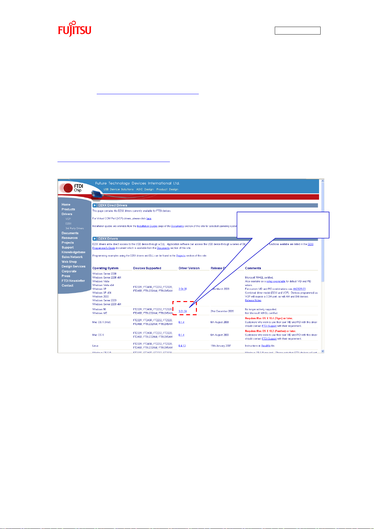
Install a USB driver.
From the FTDI web page shown below, download the Windows driver as directed in “Figure 1-3
Downloading the USB driver”.
http://www.ftdichip.com/Drivers/D2XX.htm
- 20 -
Figure 1-3 Downloading the USB driver
Page 21
AN07-00180-3E
After downloading the driver, decompress it, and then connect the board to the PC by using the USB
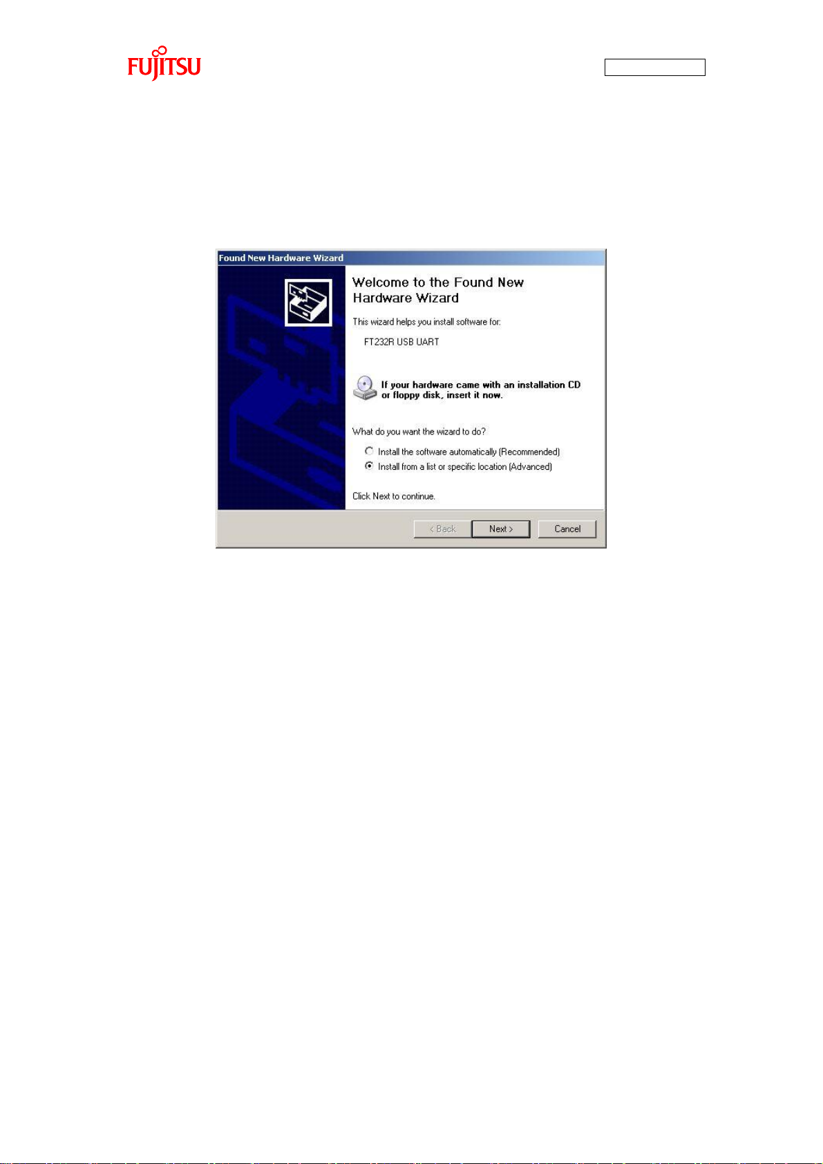
cable included in the kit. As shown in “Figure 1-4 Installing FT232R USB UART”, the dialog for
“FT232R USB UART” installation is displayed; select “Install from a list or specific location”, and then
click the “Next” button.
Figure 1-4 Installing FT232R USB UART
- 21 -
Page 22
AN07-00180-3E
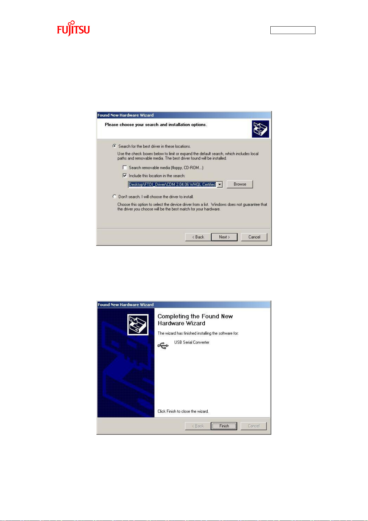
As shown in “Figure 1-5 Selecting the search locations”, to search for the installation file, check
“Search for the best driver in these locations” and “Include this location in the search” only, select the
location at which the driver was decompressed, and then click the “Next” button; installation of the driver
starts.
Figure 1-5 Selecting the search locations
When the driver installation ends, the dialog shown in “Figure 1-6 Completing the USB Serial
Converter ” is displayed; click the “Finish” button.
Figure 1-6 Completing the USB Serial Converter installation
- 22 -
Page 23
AN07-00180-3E
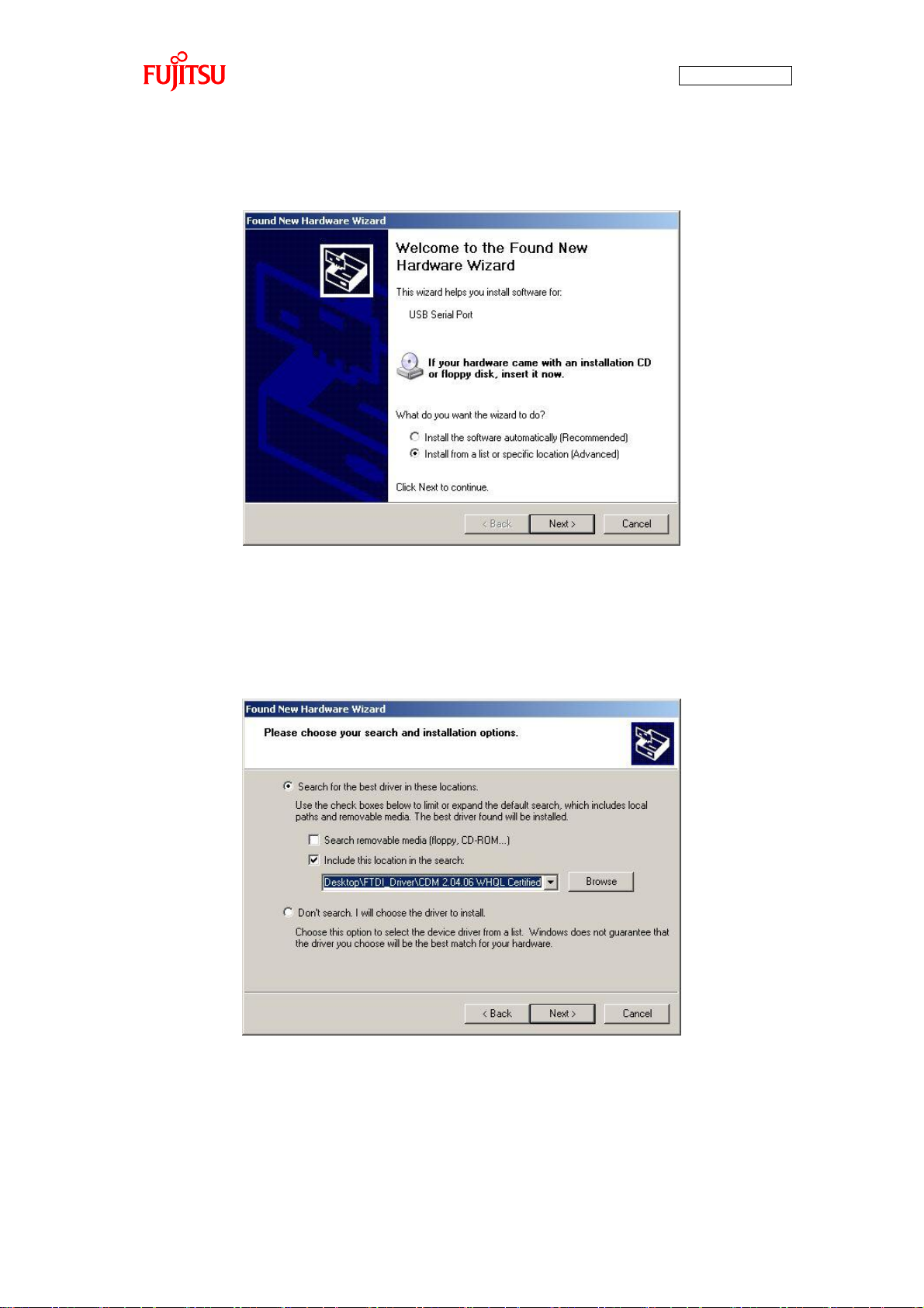
After that, as shown in “Figure 1-7 Installing USB Serial Port”, installation of “USB Serial Port” is
indicated; select “Install from a list or specific location” and then click the “Next” button.
Figure 1-7 Installing USB Serial Port
As shown in “Figure 1-8 Selecting the search locations”, to search for the installation file, check “Search
for the best driver in these locations” and “Include this location in the search” only, select the location at
which the driver was decompressed, and then click the “Next” button; installation of the driver starts.
Figure 1-8 Selecting the search locations
- 23 -
Page 24
AN07-00180-3E
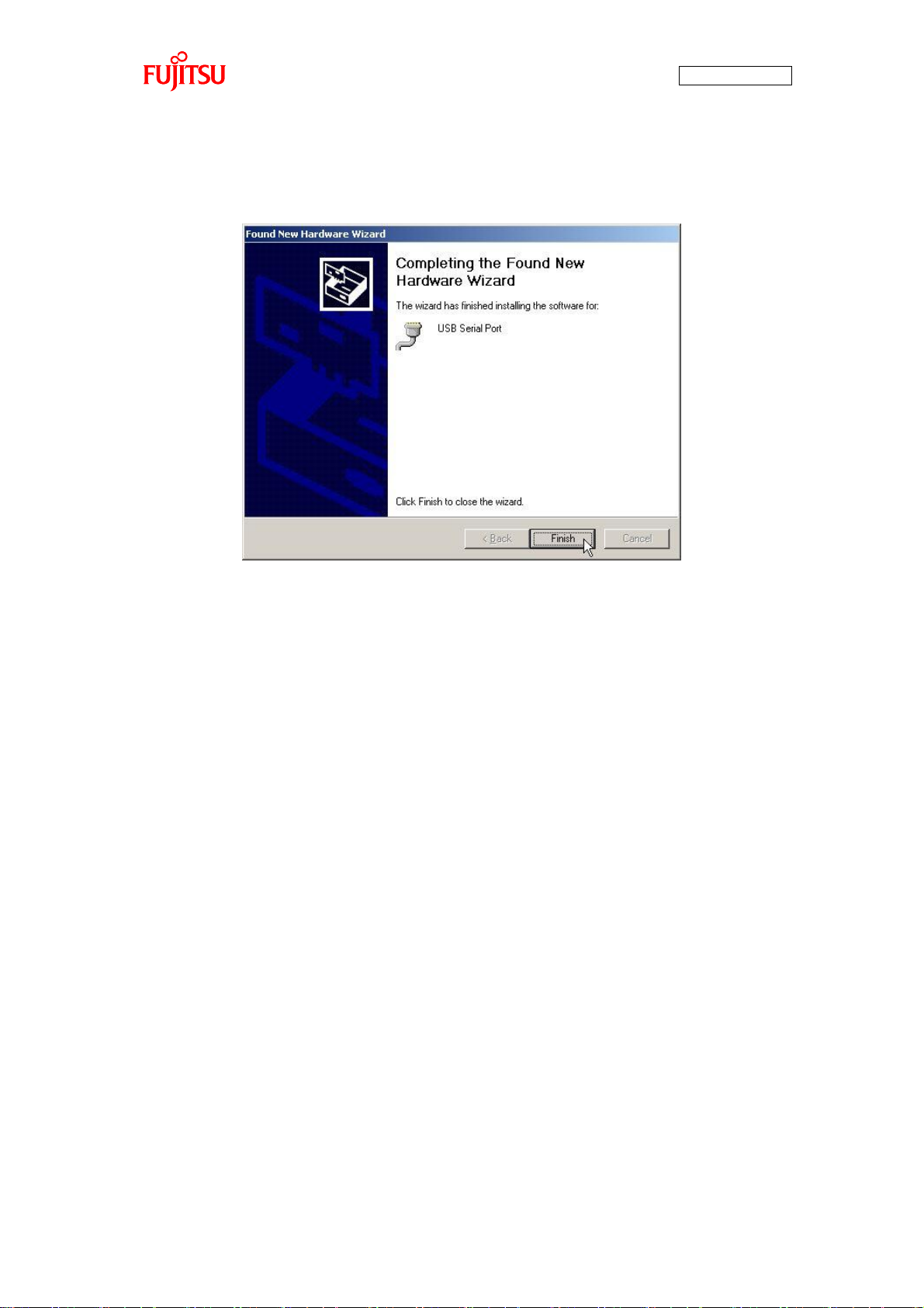
When the driver installation ends, the dialog shown in “Figure 1-9 Completing the USB Serial Port
installation” is displayed; Click the “Finish” button.
Figure 1-9 Completing the USB Serial Port installation
- 24 -
Page 25
AN07-00180-3E
1.1.3 Installing the integrated development environment SOFTUNE (bits pot dedicated
version)
Note
If SOFTUNE V6 of the product version has been installed, first uninstall it, and then install the bits
pot dedicated version.
Start installing the integrated development environment SOFTUNE. Extract the following file from the
inside of the folder extracted by “1.1.1 Downloading the software”.
¥softwares¥softune¥REV600010-BV.zip
Double-click “Setup.exe” in the decompressed folder; the dialog shown in “Figure 1-10 SOFTUNE setup
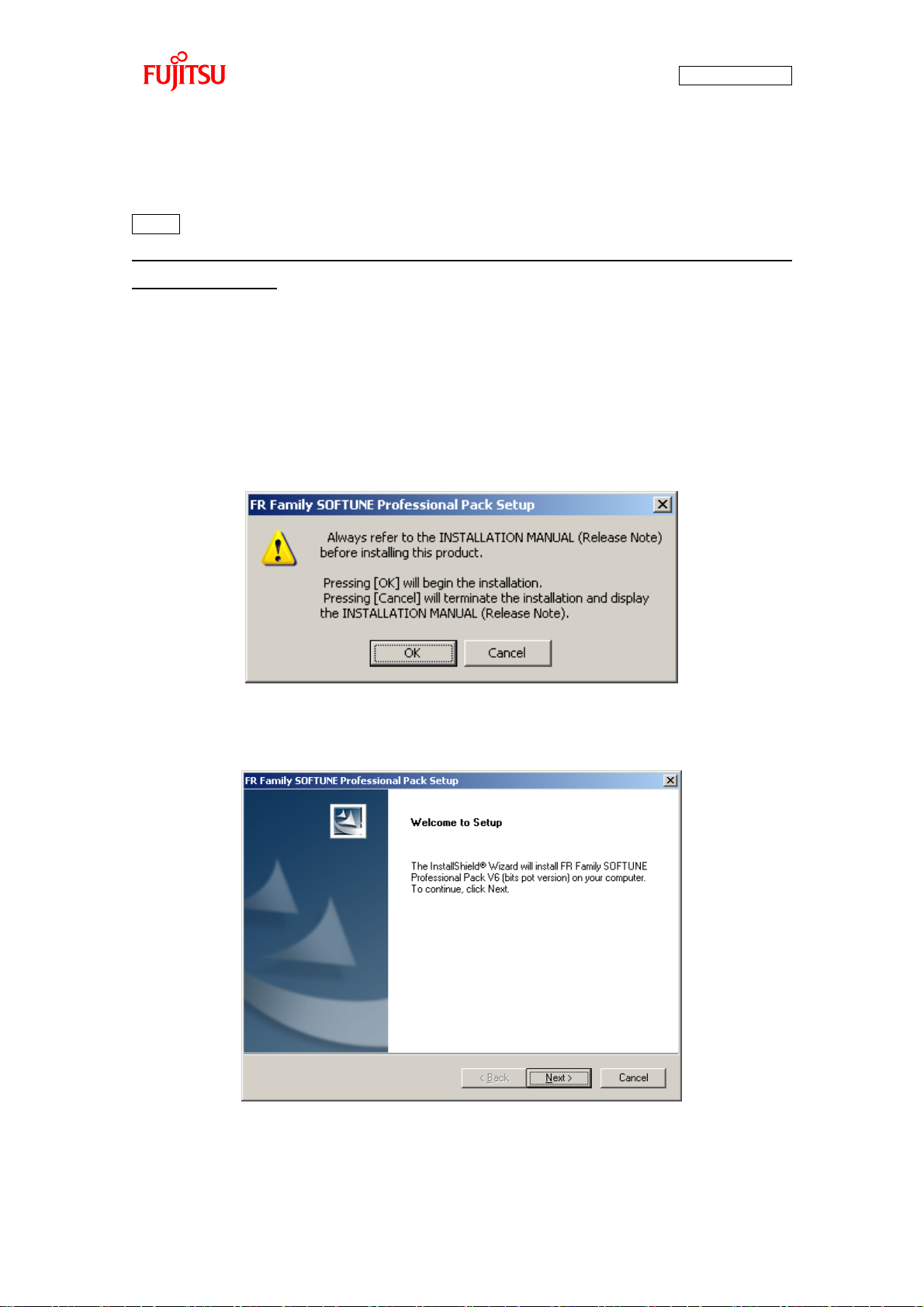
confirmation” is displayed. Click the “OK” button.
Figure 1-10 SOFTUNE setup confirmation
The setup wizard shown in “Figure 1-11 Starting SOFTUNE setup” is displayed; click the “Next” button.
Figure 1-11 Starting SOFTUNE setup
- 25 -
Page 26
AN07-00180-3E
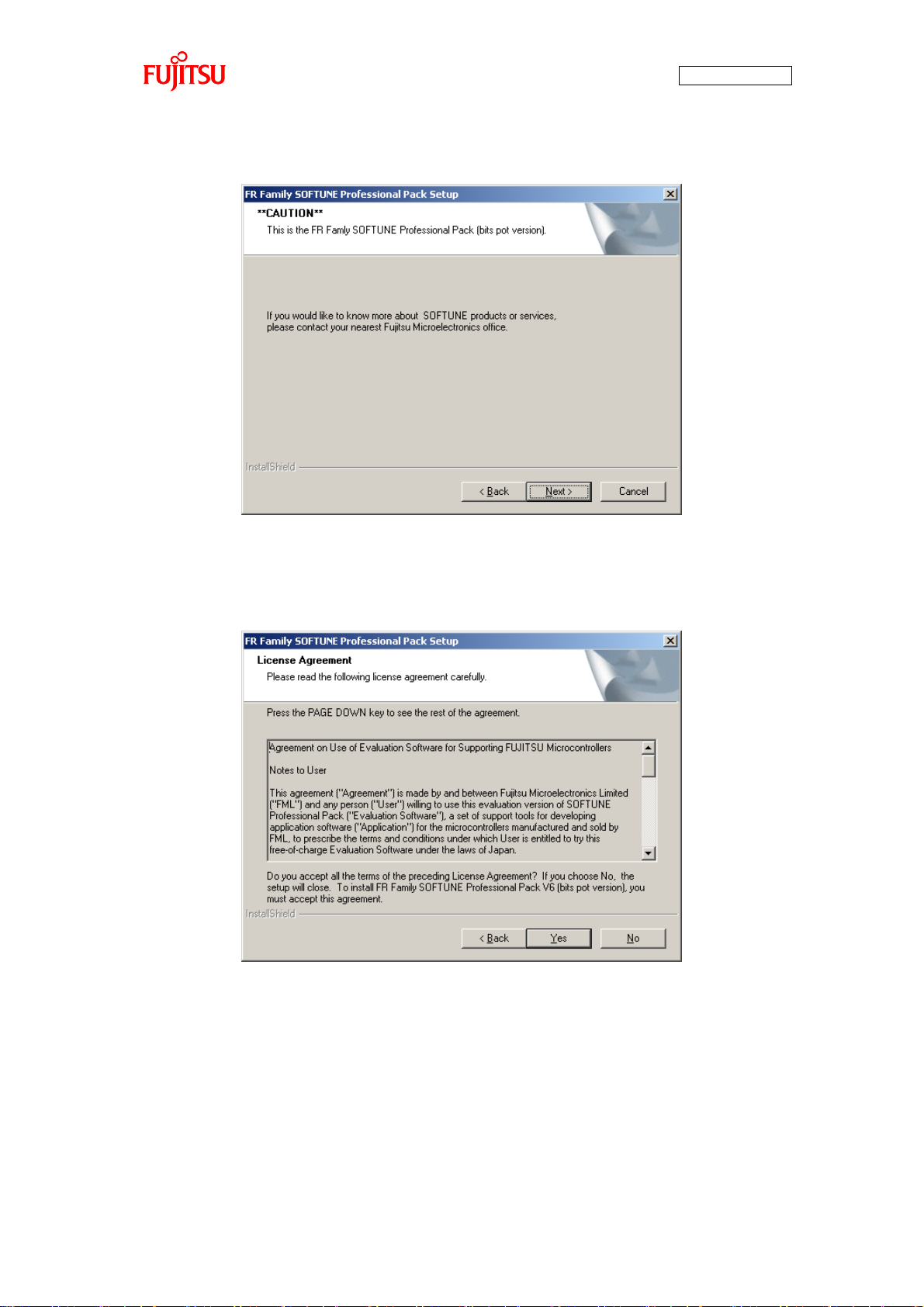
The dialog shown in “Figure 1-12 Caution on SOFTUNE setup” is displayed; click the “Next” button.
Figure 1-12 Caution on SOFTUNE setup
The dialog shown in “Figure 1-13 SOFTUNE setup/License agreement” appears; read through the
agreements and then click “Yes” button.
Figure 1-13 SOFTUNE setup/License agreement
- 26 -
Page 27
AN07-00180-3E
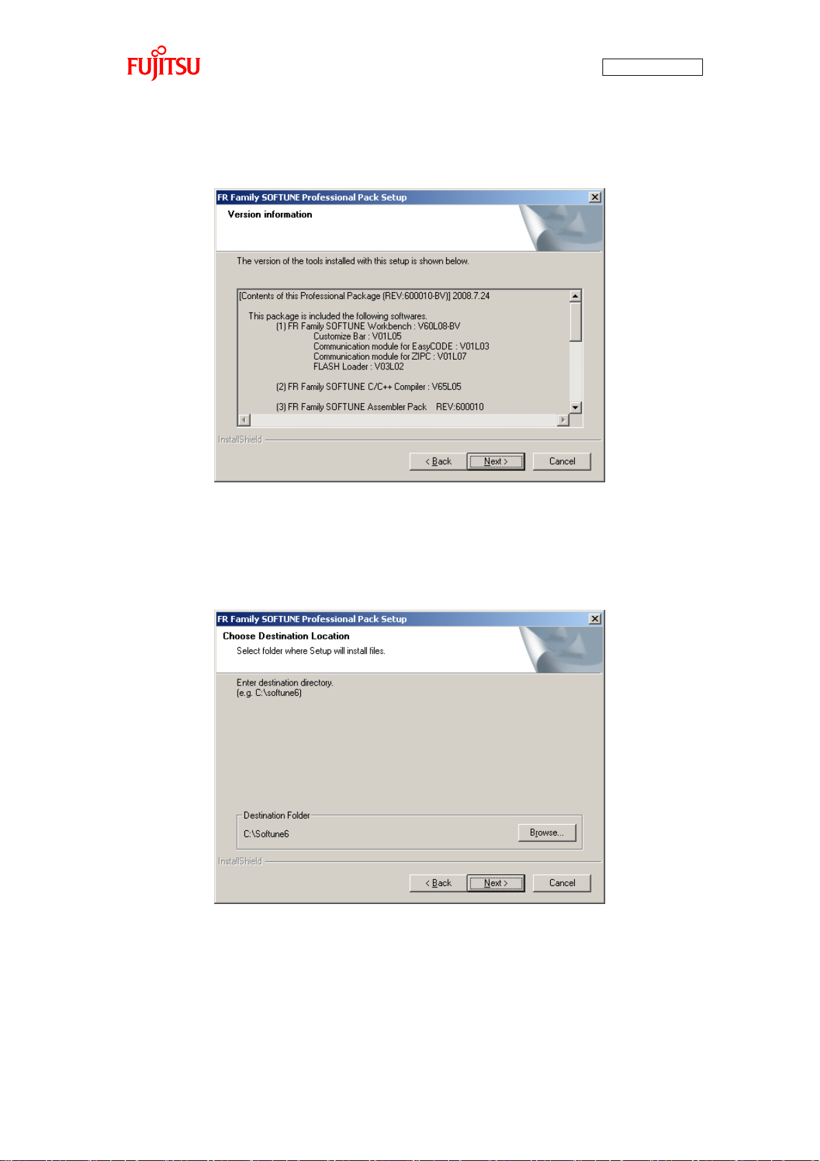
The version information is displayed as shown in “Figure 1-14 SOFTUNE setup/Version ”; click the
“Next” button.
Figure 1-14 SOFTUNE setup/Version information
The dialog about the destination of installation shown in “Figure 1-15 SOFTUNE setup/Selecting the
destination of installation” appears; select the default folder or desired folder and then click the “Next”
button.
Figure 1-15 SOFTUNE setup/Selecting the destination of installation
- 27 -
Page 28
AN07-00180-3E
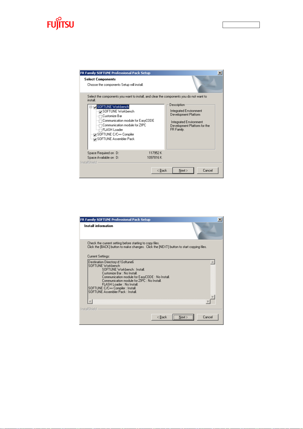
The dialog for component selection is displayed as shown in “Figure 1-16 SOFTUNE setup/Selecting the
components”; keep the default settings and then click the “Next” button.
Figure 1-16 SOFTUNE setup/Selecting the components
As shown in “Figure 1-17 SOFTUNE setup/Confirming the installation settings”, the dialog for
confirmation of the installation settings is displayed. Click the “Next” button; installation begins.
Figure 1-17 SOFTUNE setup/Confirming the installation settings
- 28 -
Page 29
AN07-00180-3E
The dialog shown in “Figure 1-18 SOFTUNE setup/Completion” appears to tell the completion of
installation; click the “Finish” button.
Figure 1-18 SOFTUNE setup/Completion
- 29 -
Page 30
AN07-00180-3E
1.1.4 Installing PC Writer (bits pot red dedicated version)
Start installing PC Writer. Confirm the following file from the inside of the folder extracted by “1.1.1
Downloading the software”.
¥softwares¥pc writer¥MB91F267NA_setup.exe
Double-click “MB91F267NA_setup.exe”; the dialog shown in “Figure 1-19 PC Writer/Installation
dialog” appears and installation starts; click the “Next” button.
Figure 1-19 PC Writer/Installation dialog
- 30 -
Page 31

AN07-00180-3E
The dialog shown in “Figure 1-20 PC Writer/Setup type” appears; select “All”, and then click the “Next”
button.
Figure 1-20 PC Writer/Setup type
The dialog shown in “Figure 1-21 PC Writer/Ready to install” appears to tell that the setup is ready to
install PC Writer; click “Install”.
Figure 1-21 PC Writer/Ready to install
- 31 -
Page 32

AN07-00180-3E
After the installation ends, the dialog shown in “Figure 1-22 Completing the PC Writer ” appears to tell
the completion of installation; click “Finish”.
Figure 1-22 Completing the PC Writer installation
- 32 -
Page 33

AN07-00180-3E
MODE selector
Operation
PRG
FLASH memory serial write mode
→Used to write a program into the microcontroller.
RUN
Single ship mode
→Used to run the program written into it.
Set the MODE selector to
“PRG”.
1.1.5 Configuring the evaluation board and connecting it to the PC
After SOFTUNE installation, configure a switch on the board and then connect it to the PC.
Set the “MODE” selector on the board to “PRG”.
Figure 1-23 MODE selection
Make sure that the MODE selector is set to “PRG”.
Then, connect it to the PC.
- 33 -
Page 34

AN07-00180-3E
After SOFTUNE installation,
connect the USB cable.
USB port
Connect a USB port on the PC.
For information about port locations and so forth, refer to the manual of the PC.
Connect the USB cable included in the kit to a USB port on the PC and the USB port on the board. Be
sure to directly connect between them without using a USB hub.
Figure 1-24 Connection between the PC and the board
The power of the board is supplied via USB (USB bus power).
[Note]
If a driver installation dialog is displayed after connecting the board to the PC, USB drivers
may be incorrectly installed.
Install drivers according to the USB driver installation manual.
- 34 -
Page 35

2 Running the program
To run a program with the starter kit, take either of the following procedures.
(1) Executing in single chip mode Go to P.36
(2) Debugging by using Monitor Debugger Go to P.43
AN07-00180-3E
- 35 -
Page 36

AN07-00180-3E
2.1 Executing in single chip mode
In single chip mode, take the following procedures.
(1) Building a project
(2) Writing the program into the microcontroller
2.1.1 Building a project
Preparation
Extract the following file from the inside of the folder extracted by “1.1.1 Downloading the software”.
¥sample programs¥bitpot_red_SampleProgram.zip
Select “Start” → “All Programs” → “Softune V6” → “FR Family Softune Workbench” to activate
SOFTUNE.
As shown in “Figure 2-1 Opening a workspace”, select the menu of SOFTUNE, “File” and then “Open
Workspace” to open a workspace.
Figure 2-1 Opening a workspace
- 36 -
Page 37

AN07-00180-3E
As shown in “Figure 2-2 Selecting a workspace”, the dialog that allows you to select a workspace is
displayed. Select the folder containing the sample program, select the workspace of
“bitpot_red_SampleProgram.wsp”, and then click “Open”.
¥bitpot_red_SampleProgram¥bitpot_red_SampleProgram.wsp
Figure 2-2 Selecting a workspace
The workspace opens; from the “project” menu, click “Build” to build it.
Figure 2-3 Building a project
- 37 -
Page 38

AN07-00180-3E
Click this.
The message pane at the bottom of the window shows a message that tells no error was found as shown in
“Figure 2-4 Completing the build” to inform you of successful build.
Figure 2-4 Completing the build
2.1.2 Writing the program into the microcontroller
Preparation
Set MODE on the board to “PRG” in advance.
Select “Start” → “All Programs” → “FUJITSU FLASH MCU Programmer” → “MB91F267NA” to
activate PC Writer.
To select a file to be written as shown in “Figure 2-5 Opening the file to write”, click the “Open” button.
Figure 2-5 Opening the file to write
- 38 -
Page 39

AN07-00180-3E
The dialog that allows you to select the file is displayed as shown in “Figure 2-6 Selecting the file to
write”; select the file built in “2.1.1 Building a project” and then click “Open”.
¥bitpot_red_SampleProgram¥Debug¥ABS¥bitpot_red_SampleProgram.mhx
Figure 2-6 Selecting the file to write
- 39 -
Page 40

AN07-00180-3E
Click this.
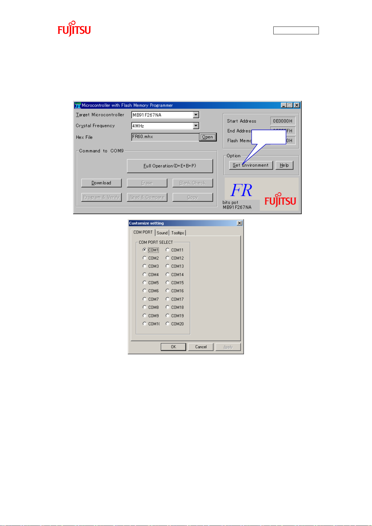
Then, select the COM port to be used for the writing. Click the “Set Environment” button; the COM port
selection dialog appears. Select the COM port with which the board is connected, and then click the “OK”
button.
Figure 2-7 Select the COM port to be used for the writing
- 40 -
Page 41

AN07-00180-3E
Check this.
To check the COM port in use, right-click “My Computer” and then select “Properties”; the system
properties are displayed. Select the “Hardware” tab and then click the “Device Manager” button.
After Device Manager activates, check the COM port number in the parentheses of “USB Serial Port
(COM n)” under “Port (COM and LPT)” in the tree shown in “Figure 2-8 Checking the COM port”.
Figure 2-8 Checking the COM port
- 41 -
Page 42

AN07-00180-3E
As shown in “Figure 2-9 Writing the program”, press the “Full Operation” button to start writing the
program; the dialog that asks you to press the Reset switch is displayed. Press the Reset SW on the board,
and then click the “OK” button on the dialog; the program write sequence starts. For the location of the
Reset SW, see “Figure 1-1 External board view”.
Figure 2-9 Writing the program
The dialog shown in “Figure 2-10 Completing the program writing” is displayed to notify you of the
completion of the program writing; press the “OK” button to quit PC Writer.
Figure 2-10 Completing the program writing
Set the MODE switch on the board to “RUN” and then press the Reset button; the program starts running.
- 42 -
Page 43

AN07-00180-3E
Click this.
2.2 Debugging by using Monitor Debugger
To debug by using Monitor Debugger, take the following procedures.
(1) Writing Monitor Debugger into the microcontroller
(2) Activating SOFTUNE and configuring the debug settings
(3) Writing the program into the microcontroller
(4) Loading the target file
(5) Running the debugger
2.2.1 Writing Monitor Debugger into the microcontroller
Preparation
Extract the following file from the inside of the folder extracted by “1.1.1 Downloading the software”.
¥sample programs¥bitpot_red_SampleProgram_md_set.zip
Select “Start” → “All Programs” → “FUJITSU FLASH MCU Programmer” → “MB91F267NA” to
activate PC Writer.
As shown in “Figure 2-11 Opening the file to write”, to select a file to be written, click the “Open”
button.
Figure 2-11 Opening the file to write
- 43 -
Page 44
AN07-00180-3E
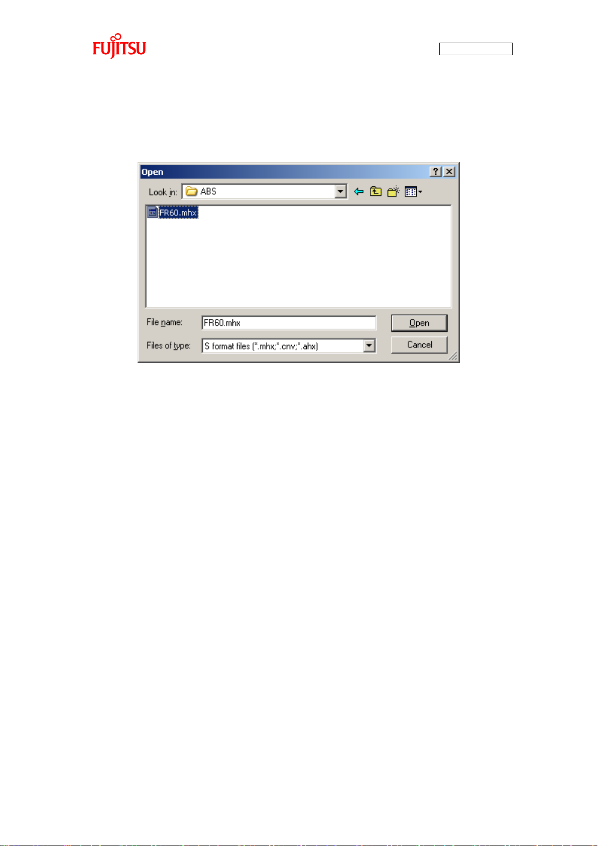
As shown in “Figure 2-12 Selecting the file to write”, the dialog that allows you to select the file to write
appears; select the file as shown below, and then click “Open”.
¥FR60¥Debug¥ABS¥FR60.mhx
Figure 2-12 Selecting the file to write
- 44 -
Page 45
AN07-00180-3E
Click this.
Then, select the COM port to be used for the writing. Click the “Set Environment” button; the COM port
selection dialog appears. Select the COM port with which the board is connected, and then click the “OK”
button.
Figure 2-13 Select the COM port to be used for the writing
- 45 -
Page 46

AN07-00180-3E
Check this.
To check the COM port in use, right-click “My Computer” and then select “Properties”; the system
properties are displayed. Select the “Hardware” tab and then click the “Device Manager” button.
After Device Manager activates, check the COM port number in the parentheses of “USB Serial Port
(COM n)” under “Port (COM and LPT)” in the tree shown in “Figure 2-14 Checking the COM port”.
Figure 2-14 Checking the COM port
- 46 -
Page 47

AN07-00180-3E
As shown in “Figure 2-15 Writing the program”, press the “Full Operation” button to start writing the
program; the dialog that asks you to press the Reset switch is displayed. Press the Reset SW on the
board, and then click the “OK” button on the dialog; the program write sequence starts. For the location
of the Reset SW, see “Figure 1-1 External board view”.
Figure 2-15 Writing the program
The dialog shown in “Figure 2-16 Completing the program writing” is displayed to notify you of the
completion of the program writing; press the “OK” button to quit PC Writer.
Figure 2-16 Completing the program writing
- 47 -
Page 48

AN07-00180-3E
2.2.2 Activating SOFTUNE and configuring the debug settings
Preparation
Set MODE on the board to “RUN” in advance, and then press the Reset button.
Select “Start” → “All Programs” → “Softune V6” → “FR Family Softune Workbench” to activate
SOFTUNE.
As shown in “Figure 2-17 Opening a workspace”, from a menu of SOFTUNE, select “File” → “Open
Workspace” to open a workspace.
Figure 2-17 Opening a workspace
- 48 -
Page 49

AN07-00180-3E
As shown in “Figure 2-18 Selecting a workspace”, the dialog that allows you to select a workspace is
displayed. Select the folder containing the sample program, select the workspace of
“bitpot_red_SampleProgram_md.wsp”, and then click “Open”.
¥bitpot_red_SampleProgram_md¥bitpot_red_SampleProgram_md.wsp
Figure 2-18 Selecting a workspace
The workspace opens; from the “project” menu, click “Build” to build it.
Figure 2-19 Building a project
- 49 -
Page 50

AN07-00180-3E
The message pane at the bottom of the window shows a message as shown in “Figure 2-20 Completing
the build”. A warning is displayed but the build has been successfully ended. (The warning indicates no
problem.)
Figure 2-20 Completing the build
Then, configure the debug settings. As shown in “Figure 2-21 Changing the debug settings”, expand
“Debug”, select “mon_38400.sup”, and then right-click on it. A menu appears; click “Change Settings”.
Figure 2-21 Changing the debug settings
- 50 -
Page 51

AN07-00180-3E
As shown in “Figure 2-22 Starting the debug setting ”, the debug setup wizard is displayed; click the
“Next” button.
Figure 2-22 Starting the debug setting wizard
Select the debugger type as shown in “Figure 2-23 Selecting the debugger type”; select “Monitor
Debugger”, and then click the “Next” button.
Figure 2-23 Selecting the debugger type
- 51 -
Page 52

AN07-00180-3E
Select the device type as shown in “Figure 2-24 Selecting the device type”. Set “RS” to the device name,
set the COM port number to which the board is connected to the port name, set “38400” to the baud rate,
and then click the “Next” button.
Figure 2-24 Selecting the device type
Specify nothing to the batch file field as shown in “Figure 2-25 Specifying a batch file”; keep the field
left blank and click the “Next” button.
Figure 2-25 Specifying a batch file
- 52 -
Page 53

AN07-00180-3E
Just ignore the target file settings as shown in “Figure 2-26 Configuring the target file settings”; click the
“Next” button.
Figure 2-26 Configuring the target file settings
As shown in “Figure 2-27 Setting setup file selection”, select “Specify” for setup file selection, and then
click the “Next” button.
Figure 2-27 Setting setup file selection
- 53 -
Page 54

AN07-00180-3E
On the dialog shown in “Figure 2-28 Completing the setup wizard”, click the “Finish” button to finish
configuring the settings.
Figure 2-28 Completing the setup wizard
Start debugging as shown in “Figure 2-29 Start debugging”.
Figure 2-29 Start debugging
- 54 -
Page 55

AN07-00180-3E
2.2.3 Writing the program into the microcontroller
As shown in “Figure 2-30 Showing the commands window”, from the “View” menu, select “Commands”
to show the program window.
Figure 2-30 Showing the commands window
- 55 -
Page 56

AN07-00180-3E
Input the following command into the field as shown in “Figure 2-31 Inputting commands”, and then
click the “Enter” button. The program is started to be written.
bat FshLdWrt.prc
Figure 2-31 Inputting commands
As shown in “Figure 2-32 Completing the program writing”, the command window shows “Write Flash
Memory Success” to notify you of successful completion of the program writing into the microcontroller.
Figure 2-32 Completing the program writing
- 56 -
Page 57

AN07-00180-3E
2.2.4 Loading the target file
As shown in “Figure 2-33 Loading the target file”, from the “Debug” menu, select “Load Target File”.
The target file is loaded; you can set break points at desired points.
Figure 2-33 Loading the target file
- 57 -
Page 58

AN07-00180-3E
Click this to set a break point.
To cancel the break point, click this again.
2.2.5 Running the debugger
As shown in “Figure 2-34 Setting break points”, you can set break points to lines with a green round mark
on the left side in the source file. Note that you cannot set break points while the program is running.
Figure 2-34 Setting break points
As shown in “Figure 2-35 Running the program”, click the “Run Continuously” icon to run the program.
Figure 2-35 Running the program
- 58 -
Page 59

AN07-00180-3E
As shown in “Figure 2-36 Stopping the program”, click the × button for closing the application on the
upper right side of the window to stop running the program.
Although a warning dialog for the stop is displayed, click the “Abort” button in any case.
Figure 2-36 Stopping the program
2.2.6 Notes on Monitor Debugger
Note that Monitor Debugger has the following restrictions.
・ Only up to 16 break points can be set. No more break point can be set, so to set other break points,
cancel some of those already set and set new break point.
・ While Monitor Debugger is running (after Monitor Debugger is activated in 2.2.2 Activating
SOFTUNE and configuring the debug settings), it is prohibited to press the Reset SW on the board;
it causes Monitor Debugger to stop.
・ For the operation of Monitor Debugger, UART0 is used. If you modify the sample program or
apply it to some other purpose, remind this.
- 59 -
Page 60

AN07-00180-3E
3 Operation of the sample program
This section describes the operation of the sample program. The operation of the sample is classified into
the following two categories.
(1) bits pot red single-unit operation
(2) CAN communication operation (CAN communication operation with the bits pot white)
- 60 -
Page 61

AN07-00180-3E
(1) Mode SW
(2) Reset SW
(3) SW2
(4) SW3
(5) SW5
(6) Temperature
sensor
(7) LEDs (green)
(8) LEDs (red)
(9) BLDC motor
3.1 bits pot red single-unit operation
“Figure 3-1 Single-unit operation/Controls and mechanicals” shows the controls and mechanicals, and
“Table 3-1 Single-unit operation/Descriptions of the controls and mechanicals” provides descriptions
about them.
SW2, SW3, SW5, and temperature sensor on the board control the operations of the green and red LEDs
and BLDC motor.
Figure 3-1 Single-unit operation/Controls and mechanicals
- 61 -
Page 62

AN07-00180-3E
No.
Name
Function
Description
(1)
Mode SW
Control
Switches between RPG mode and RUN mode.
PRG: Write a program
RUN: Run the program
(2)
Reset SW
Control
Rests the MCU when pressed.
(3)
SW2
Control
Rotates/stops the motor in turn when pressed. The
motor rotates if it is stopped and stops if it is rotating
when this switch is pressed.
(4)
SW3
Control
Brakes the (stops) motor if it is rotating when pressed.
The brake is applied while the switch is pressed.
Releasing the switch turns off the brake and the motor
starts rotating.
(5)
SW5
Control
Selects the direction of the motor rotation.
Right side: The motor rotates clockwise.
Left side: The motor rotates counterclockwise.
(6)
Temperature sensor
Control
Changes the rotation speed according to information
from the temperature sensor.
When the temperature rises, the rotation speed
increases.
When the temperature falls, the rotation speed
decreases.
(7)
LEDs (green)
Mechanical
Indicate the status of whether the motor driver circuit is
ON/OFF.
(8)
LEDs (red)
Mechanical
Indicate the status of whether the hall elements are
ON/OFF.
(9)
BLDC motor
Mechanical
Operates according to rotation/stop by the SW2.
The brake, rotation direction, and rotation speed
respectively depend on the SW3, SW5, and temperature
sensor.
Table 3-1 Single-unit operation/Descriptions of the controls and mechanicals
- 62 -
Page 63

AN07-00180-3E
④ CAN 送信 LED
⑤ CAN 受信 LED
(6) LEDs (green)
(7) LEDs (red)
(2) Reset SW
(3) Temperature
sensor
(8) BLDC motor
(1) Mode SW
3.2 CAN communication operation (CAN communication operation with the
bits pot white)
“Figure 3-2 CAN communication operation/Controls and mechanicals” shows the controls and
mechanicals, and “Table 3-2 CAN communication operation/Descriptions of the controls and
mechanicals” provides descriptions about them.
The bits pot white performs CAN communication, and on execution of a motor operation command, the
green and red LEDs and BLDC motor work. On execution of a temperature measurement command, the
temperature is returned from the temperature sensor.
Figure 3-2 CAN communication operation/Controls and mechanicals
- 63 -
Page 64

No.
Name
Function
Description
(1)
Mode SW
Control
Switches between RPG mode and RUN mode.
PRG: Write a program
RUN: Run the program
(2)
Reset SW
Control
Rests the MCU when pressed.
(3)
Temperature sensor
Control
Returns the temperature measured by this temperature
sensor on a temperature measurement command in
CAN communication.
(4)
CAN transmit LED
Mechanical
Lights when a CAN transmit is performed.
(5)
CAN receive LED
Mechanical
Lights when a CAN receive is performed.
(6)
LEDs (green)
Mechanical
Indicate the status of whether the motor driver circuit is
ON/OFF.
(7)
LEDs (red)
Mechanical
Indicate the status of whether the hall elements are
ON/OFF.
(8)
BLDC motor
Mechanical
Operates according to rotation/stop by motor operation
commands. The brake, rotation direction, and rotation
speed respectively depend on motor operation
commands.
Table 3-2 CAN communication operation/Descriptions of the controls and mechanicals
AN07-00180-3E
- 64 -
Page 65

AN07-00180-3E
(a) DC motor configuration example
(b) BLDC motor configuration example
Microcontroller
Driver circuit
Coil
Hall element
4 Try to rotate the BLDC motor
In these days, motors are indispensable in our daily life. Motors are now used in various places, for
example, air conditioners, compressors of refrigerators, turn tables of CD and DVD drives, and wipers
and door mirrors of vehicles.
This chapter provides descriptions about how to rotate the BLDC motor by using a microcontroller
macro.
4.1 What is the BLDC motor?
The BLDC motor is a DC brushless motor that is a type of motors. In distinction from generally known
DC motors, the DC brushless motor has no brush, longer life, and low electric noise, so it tends to be
suitable for miniaturization. Uses of the DC brushless motor are still increasing.
Rotation of both the DC motor and BLDC motor is controlled by the currents from a DC power supply.
The DC motor switches the direction of the rotor coil current by using brushes (communitator) to change
the magnetic flux for rotation control. On the other hand, the BLDC motor has no brush. As shown in
“Figure 4-1 DC motor/BLDC motor configuration examples”, it switches the directions of the stator coil
currents by using switches to change the magnetic fluxes for rotation control. To do this switching, the
microcontroller is used. For detection of the rotor position, hall elements are used.
This board has a driver circuit, so you can starts rotating the BLDC motor immediately.
- 65 -
Figure 4-1 DC motor/BLDC motor configuration examples
Page 66

AN07-00180-3E
Microcontroller
V-phase
U-phase
W-phase
V-High
W-High
W-Low
V-Low
U-Low
Hall-U
Hall-V
Hall-W
4.2 How does the BLDC motor rotate?
The BLDC motor has three phases different by 120°. As shown in “Figure 4-2 Names of the respective
elements”, the phases are called the U-phase, V-phase, and W-phase respectively.
The switches on the driver circuit are respectively called U-High, U-Low, V-High, V-Low, W-High, and
W-Low and connected as outputs from the microcontroller. The hall elements for detection of the rotor
position are respectively called Hall-U, Hall-V, and Hall-W and connected as inputs to the
microcontroller.
Figure 4-2 Names of the respective elements
By turning on/off the switches, the directions of the currents conducted to the motor are controlled. Two
of the three coils are set to positive or negative to generate a magnetic field for motor rotation.
The hall elements are used to detect the position of the rotor by 60° and the detection is represented with
1 or 0. According to their values, the switches are turned on/off. On detection of the hall elements, the
High side of the phase corresponding to it is turned ON, and on no detection, the Low side is turned ON.
“Figure 4-3 120° conduction method time chart” shows their relationship.
This way of driving control is called the 120° conduction method (square-weave control).
- 66 -
Page 67

AN07-00180-3E
Hall-U
Hall-V
Hall-W
U-High
U-Low
V-High
V-Low
W-High
W-Low
U
V
W
1
0 1 0 1 0
ON
ON
ON
ON
ON
ON + - + + - -
0°
120°
240°
360°
480°
Figure 4-3 120° conduction method time chart
- 67 -
Page 68

AN07-00180-3E
Same as RTO0/RTO1
Same as RTO0/RTO1
Anode
Anode
Cathode
Cathode
4.3 BLDC motor rotation control by the microcontroller
This section describes how the BLDC motor is practically controlled with the 120° conduction method by
the microcontroller.
On the board, as shown in “Figure 4-4 Motor driver circuit”, the microcontroller is connected with the
motor driver circuit. The relationship of the connections with the semiconductor elements described in
“4.2 How does the BLDC motor rotate?” is as shown in “Table 4-1 Microcontroller pin/Motor driver
circuit connections”. By turning RTO0 to 5 on/off according to the positions of the hall elements as
shown in “Figure 4-3 120° conduction method time chart”, the motor can be rotated.
Figure 4-4 Motor driver circuit
- 68 -
Page 69

AN07-00180-3E
Microcontroller
pin number
Pin name
Name of the semiconductor
element connected
Pin57
RTO0
U-High
Pin56
RTO1
U-Low
Pin55
RTO2
V-High
Pin54
RTO3
V-Low
Pin53
RTO4
W-High
Pin52
RTO5
W-Low
Function name
Description
16-bit free-run timer
Timer in which an up/down counter is used.
This counter is used to configure the output compare function.
16-bit output compare
Used to make comparisons with the value of the free-run timer,
and the resulting values are used to turn on/off RTO0 to 5.
TCCSH0
ECKE
IRQZF
IRQZE
MSI2
MSI1
MSI0
ICLR
ICRE
TCCSL0
BFE
STOP
MODE
SCLR
CLK3
CLK2
CLK1
CLK0
Timer control high-order bits
bit15
bit14
bit13
bit12
bit11
bit10
bit9
bit8
Timer control low-order bits
bit7
bit6
bit5
bit4
bit3
bit2
bit1
bit0
Table 4-1 Microcontroller pin/Motor driver circuit connections
RTO0 to 5 ON/OFF control is practically taken by the macro in the microprocessor mounted on the board.
So, it is necessary to configure registers for functions employed by the macro. “Table 4-2 Functions
employed by the motor driving macro” shows the functions employed.
Table 4-2 Functions employed by the motor driving macro
The registers used for the 16-bit free-run timer are as shown in “Figure 4-5 Timer control registers”. A
description of the registers and their setting values in the sample program are as described in “Table 4-3
Description of the timer control registers and setting values”. For more information of the registers, refer
to the microcontroller hardware manual.
Figure 4-5 Timer control registers
- 69 -
Page 70

AN07-00180-3E
Register name
Setting value [function]
Description
TCCSH0_ECKE
0 [internal clock]
Clock select bit
TCCSH0_IRQZF
0 [bit clear]
0 detection interrupt flag bit
TCCSH0_IRQZE
0 [interrupt request disable]
0 detection interrupt request enable bit
TCCSH0_MSI2
-
Interrupt mask select bits
Not used
TCCSH0_MSI1
-
TCCSH0_MSI0
-
TCCSH0_ICLR
0 [bit clear]
Compare clear interrupt flag bit
TCCSH0_ICRE
1 [interrupt request enable]
Compare clear interrupt request enable
bit
TCCSL0_BFE
1 [compare clear buffer enable]
Compare clear buffer enable bit
TCCSL0_STOP
1 [counter stop]
Timer enable bit
TCCSL0_MODE
1 [up/down count mode]
Timer counter mode bit
TCCSL0_SCLR
1 [counter initialization to 0000]
Timer clear bit
TCCSL0_CLK3
0 [62.5 ns]
Clock frequency select bits
TCCSL0_CLK2
0 [↑]
TCCSL0_CLK1
0 [↑]
TCCSL0_CLK0
0 [↑]
Table 4-3 Description of the timer control registers and setting values
- 70 -
Page 71

AN07-00180-3E
CPCLRB0
CL15
CL14
CL13
CL12
CL11
CL10
CL9
CL8
CL7
CL6
CL5
CL4
CL3
CL2
CL1
CL0
Compare clear buffer register
bit15
bit14
bit13
bit12
bit11
bit10
bit9
bit8
bit7
bit6
bit5
bit4
bit3
bit2
bit1
bit0
OCCPB0 to
OCCPB 5
OP15
OP14
OP13
OP12
OP11
OP10
OP9
OP8
OP7
OP6
OP5
OP4
OP3
OP2
OP1
OP0
Output compare buffer register
bit15
bit14
bit13
bit12
bit11
bit10
bit9
bit8
bit7
bit6
bit5
bit4
bit3
bit2
bit1
bit0
OCMOD
-
-
MOD15
MOD14
MOD13
MOD12
MOD11
MOD10
Compare mode control register
bit15
bit14
bit13
bit12
bit11
bit10
bit9
bit8
OCSH1,3,5
BTS1
BTS0
CMOD
OTE1
OTE0
OTD1
OTD0
IOP1
IOP0
IOE1
IOE0
BUF1
BUF0
CST1
CST0
Compare control register high-order bit/s
bit15
bit14
bit13
bit12
bit11
bit10
bit9
bit8
bit7
bit6
bit5
bit4
bit3
bit2
bit1
bit0
Compare control register low-order bit/s
OCSL0,2,4
The registers used for the 16-bit output compare function are as shown in “Figure 4-6 Output compare
registers”. A description of the registers and their setting values in the sample program are as described in
“Table 4-4 Description of the output compare registers and setting values”. For more information of the
registers, refer to the microcontroller hardware manual.
Figure 4-6 Output compare registers
- 71 -
Page 72

AN07-00180-3E
Register name
Setting value [function]
Description
CPCLRB0
1599
Compare value setting
OCCPB0
1598
Output compare value settings
OCCPB1
1000
OCCPB2
1598
OCCPB3
1000
OCCPB4
1598
OCCPB5
1000
OCMOD
0xFF [1 output on a match]
Designation of the operation on a compare
match
OCSH1,3,5_BTS1
1 [transfer on a compare clear
match]
Buffer transfer select bit (ch 1,3,5)
OCSH1,3,5_BTS0
1 [transfer on a compare clear
match]
buffer transfer select bit (ch 0,2,4)
OCSH1,3,5_CMOD
1 [ inversion mode]
Output level inversion mode bit
OCSH1,3,5_OTE1
0 [general-purpose output port]
Output enable bit (ch 1,3,5)
OCSH1,3,5_OTE0
0 [general-purpose output port]
Output enable bit (ch 0,2,4)
OCSH1,3,5_OTD1
0 [1 output]
Output level bit (ch 1,3,5)
OCSH1,3,5_OTD0
0 [1 output]
Output level bit (ch 0,2,4)
OCSL0,2,4_IOP1
0 [bit clear]
Compare match interrupt flag bit (ch 1,3,5)
OCSL0,2,4_IOP0
0 [bit clear]
Compare match interrupt flag bit (ch 0,2,4)
OCSL0,2,4_IOE1
0 [compare match interrupt
disable]
Compare match interrupt enable bit (ch 1,3,5)
OCSL0,2,4_IOE0
0 [compare match interrupt
disable]
Compare match interrupt enable bit (ch 0,2,4)
OCSL0,2,4_BUF1
0 [compare buffer enable]
Compare buffer disable bit (ch 1,3,5)
OCSL0,2,4_BUF0
0 [compare buffer enable]
Compare buffer disable bit (ch 0,2,4)
OCSL0,2,4_CST1
0 [compare operation disable]
Compare operation enable bit (ch 1,3,5)
OCSL0,2,4_CST0
1 [compare operation enable]
Compare operation enable bit (ch 0,2,4)
Table 4-4 Description of the output compare registers and setting values
- 72 -
Page 73

AN07-00180-3E
Register name
Switching
OCCPB0
U-High
OCCPB1
U-Low
OCCPB2
V-High
OCCPB3
V-Low
OCCPB4
W-High
OCCPB5
W-Low
CPCLRB0 value
0
Carrier peak
(occurrence of an interrupt)
Carrier button
Time→
Initialize the 16-bit free-run timer and 16-bit output compare functions as shown in “Table 4-3
Description of the timer control registers and setting values”, “Table 4-4 Description of the output
compare registers and setting values”.
After the initialization, running the 16-bit free-run timer starts a count up using the value configured to
CPCLRB0 as the carrier peak as shown in “Figure 4-7 Operation of the free-run timer”. When the carrier
peak is reached, an interrupt takes place, and according to information about the hall elements on that
occasion, the outputs are switched on/off through comparisons with the output compare values.
After that, a countdown to the carrier bottom (0) is performed. When the count reaches 0, a count up
starts again, and this sequence is repeated.
Figure 4-7 Operation of the free-run timer
The output compare values are respectively configured by OCCPB0-5. According to the values, the
outputs of U-High, U-Low, V-High, V-Low, W-High, and W-Low are turned on/off by the macro. “ Table
4-5 Correspondence between the output compare values and the switchings” shows their association. In
addition to that, “Figure 4-8 U-High output to output comparisons” shows an example of the U-High
output.
Table 4-5 Correspondence between the output compare values and the switchings
- 73 -
Page 74

AN07-00180-3E
CPCLRB0 value
0
Time→
OCCPB0 value
U-High
Figure 4-8 U-High output to output comparisons
- 74 -
Page 75

AN07-00180-3E
Microcontrolleri nitialization
Motor macro initialization
Start
Infinite loop
Press of SW2
Start of the free-run timer
Timer running
Timer interrupt
4.4 Understanding and running the program for the BLDC motor operation
This section provides descriptions of the sample program that can really serve to operate the BLDC
motor.
“Figure 4-9 Motor operation flowchart” shows the sequence of the sample program flow. First, the
microcontroller is initialized, and then the motor macro is initialized. After that, the program goes into a
loop. In the loop, pressing SW2 starts the free-run timer and the motor macro starts operating.
When SW2 is pressed again, the free-run timer stops.
Figure 4-9 Motor operation flowchart
- 75 -
Page 76

AN07-00180-3E
/* CAN communication use (1), or unused (0) */
#define CAN_PERMIT (0)
/* Temperature sensor use (1), or unused (0) */
#define TEMP_SENSOR_USE (1)
←CAN
←Temperature sensor
void main(void)
{
(omitted);
sysInitialize();
(omitted)
mtInitialize();
(omitted)
/* main loop */
while (1)
{
(omitted)
}
}
←Microcontroller initialization
←Motor macro initialization
←Infinite loop
Now, take a look at the details of the program.
Look into the following folder of the sample program. There are some files stored in it. At first, open
MAIN.C first.
¥bitpot_red_SampleProgram¥Debug¥SRC
Look at around Line 40 that looks “Figure 4-10 Operation mode settings” for operation mode selection.
There are #define settings that enable (1) or disable (0) CAN and temperature sensor.
In this program, CAN is not to be used and the temperature sensor is to be used.
As shown in “Figure 4-11 Main function”, there is the main function around Line 131. In it, there are
“microcontroller initialization”, “motor macro initialization”, and “infinite loop”.
- 76 -
Figure 4-10 Operation mode settings
Figure 4-11 Main function
Page 77

AN07-00180-3E
__interrupt void IRQ_ext_0(void)
{
(omitted)
if(gMtStatus == MTST_STOP){
(omitted)
TCCSL0_STOP = 0;
}else{
(omitted)
TCCSL0_STOP = 1;
}
(omitted)
}
←Start of the free-run timer
←Stop of the free-run timer
__interrupt void IRQ_FreeRunComp(void)
{
if(TCCSH0_ICLR == 1) /* if OCU interrupt */
{
mtPWMController();
(omitted)
}
}
←Macro configuration
When SW2 is pressed, an interrupt takes place. Around Line 763 in MAIN.C, the interrupt function
IRQ_ext_0 is invoked as shown in “Figure 4-12 SW2 interrupt”. In it, the register value of
TCCSL0_STOP, which is used to start/top the free-run timer, is changed.
Once the free-run timer starts running, the timer interrupt function IRQ_FreeRunComp of motor_drv.c is
invoked on every carrier peak as shown in “Figure 4-13 Free-run timer interrupt”. In it, the status of the
hall elements is checked and configured into the macro.
Figure 4-12 SW2 interrupt
- 77 -
Figure 4-13 Free-run timer interrupt
Page 78
AN07-00180-3E
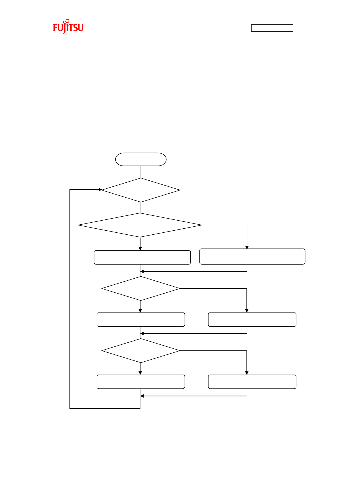
Start
Infinite loop
Speed calculation with the temperature sensor
Use of the temperature sensor
Speed calculation with the programmed variables
Press of SW3
Brake released
SW set to the right
Brake applied
Left rotation
Right rotation
false
false
false
true
true
true
4.5 Handling controls of the BLDC motor
You were able to rotate the BLDC motor by using the microcontroller macro. Then, try to control the
rotation speed, brake, and rotation direction now.
In the sample program, the controls are handled in the infinite loop inside the main function shown in
“Figure 4-11 Main function”.
The rotation speed is determined according to the temperature sensor or input from programmed variables,
and the brake is applied whether SW3 is pressed. The direction of motor rotation is determined according
to the position of SW5. “Figure 4-14 Motor controls flowchart” illustrates how the controls are handled.
- 78 -
Figure 4-14 Motor controls flowchart
Page 79

AN07-00180-3E
void main(void)
{
(omitted)
/* main loop */
while (1)
{
if (!gCanEnableFlag)
{
/* Set motor turn speed */
if (gTempEnableFlag)
{
/* get an A/D channel */
ad = adGetValue();
ad = ad > TEMP_AD_VALUE_00 ? TEMP_AD_VALUE_00 : ad;
ad = ad < TEMP_AD_VALUE_09 ? TEMP_AD_VALUE_09 : ad;
/* calc motor turn speed */
gMtSpeedMax = TEMP_AD_VALUE_00 - TEMP_AD_VALUE_09;
gMtRevSpeed = gMtSpeedMax - (ad - TEMP_AD_VALUE_09);
(omitted)
}
else
{
gMtRevSpeed = 512;
gMtSpeedMax = 1024;
}
(omitted)
mtSetDuty(gMtRevSpeed,gMtSpeedMax);
}
(omitted)
}
}
←Calculation of the rotation
speed according to the
←Calculation of the rotation speed according to
the programmed variables
←Speed setting
The rotation speed routine is written around Line 166 in the MAIN.C main function as shown in “Figure
4-15 Rotation speed control”.
When the temperature sensor is used, the rotation speed is determined in the range of 0 to 100% by a
conversion according to the A/D value obtained from the temperature sensor and the upper limit. When
the programmed variables are used, the rotation speed is determined in the range of 0 to 100% by a
conversion according to the specified current and upper limit values.
Figure 4-15 Rotation speed control
- 79 -
Page 80

AN07-00180-3E
void main(void)
{
(omitted)
/* main loop */
while (1)
{
if (!gCanEnableFlag)
{
(omitted)
/* Set motor break */
if(gMtStatus == MTST_MOVE)
{
/* Set the Motor Start Flag */
if (PDR4_P41)
{
OCSH1_OTE0 = 1;
OCSH1_OTE1 = 1;
OCSH3_OTE0 = 1;
OCSH3_OTE1 = 1;
OCSH5_OTE0 = 1;
OCSH5_OTE1 = 1;
TCCSL0_STOP = 0;
}
else
{
OCSH1_OTE0 = 0;
OCSH1_OTE1 = 0;
OCSH3_OTE0 = 0;
OCSH3_OTE1 = 0;
OCSH5_OTE0 = 0;
OCSH5_OTE1 = 0;
PDR3 = 0x00;
TCCSL0_STOP = 1;
}
}
(omitted)
}
(omitted)
}
}
←Brake released
←Brake applied
The brake control routine is written around Line 192 in the MAIN.C main function as shown in “Figure
4-16 Brake control”.
While SW3 is pressed, the outputs to all the semiconductor elements are set to off and the brake is applied
to the motor.
- 80 -
Figure 4-16 Brake control
Page 81

AN07-00180-3E
void main(void)
{
(omitted)
/* main loop */
while (1)
{
if (!gCanEnableFlag)
{
(omitted)
/* Motor Rev Direction */
gMtRevDir = PDR2_P27;
/* Set Value */
gDirection = gMtRevDir;
(omitted)
}
(omitted)
}
}
←Acquisition of the rotation direction
←Configuration of the rotation direction
The rotation direction routine is written around Line 221 in the MAIN.C main function as shown in
“Figure 4-17 Rotation direction control”.
When SW5 is set to the right side, the motor rotates to the right, and when it is set to the left side, the
motor rotates to the left.
- 81 -
Figure 4-17 Rotation direction control
Page 82

AN07-00180-3E
Legend
CAN application
CAN bus
Light
Fuel
Air conditioner
Instrument panel
Power steering
Door
Door
Door
Door
Engine
5 Try to use CAN communication
Communication is to send/receive information. There are various types of communication such as
utterance/hearing of spoken words, writing/reading of written letters, and electrical transmission of
information.
Among them, there are various standards for communication based on electrical transmission. This
chapter describes a communication standard called CAN.
CAN is a global standard of the ISO (International Organization for Standardization).
5.1 What is CAN?
CAN stands for Controller Area Network, which is an on-board LAN specification proposed by Bosch in
Germany. It is the most popular on-board control LAN and used in various parts of a vehicle as shown in
“Figure 5-1 Example of on-board CAN application”.
It is now also used not only in vehicles but also in many industries.
Figure 5-1 Example of on-board CAN application
- 82 -
Page 83

Voltage
Logical “1”
Recessive
Logical “1”
Recessive
Logical “0”
Dominant
The features of CAN can be classified into the following five points.
1. Multi-master communication
CAN employs the multi-master system in which each node is allowed to start communication as
desired. The timing of a start of communication is occurrence of an event. The word “event”
mentioned here indicates an occasion at which a node needs to start communication.
CAN avoid conflicts in communication through mediation with node signals if more than one
event occurs on nodes simultaneously. This mediation is called arbitration.
2. Bus-type topology
The CAN topology is the bus type. The maximum number of nodes depends on the
communication speed; in the case of 1M bits/sec, up to 30 nodes are allowed. This is specified as
a regulation.
3. Differential transmission system
Taking account of influence from noise on the transmission paths, CAN employs the differential
AN07-00180-3E
transmission system in which the voltage difference between two signal lines is used to
determine “0”/”1”. The signal lines are respectively called CANH and CANL and the voltage
difference between them is used to determine the bus level. The differential is used to determine
logical “0”/”1”. As shown in “Figure 5-2 CAN bus signal levels”, the bus status of logical “0” is
called dominant and the bus status of logical “1” is called recessive. The communicable distance
depends on the communication speed; in the case of 1M bits/sec, up to 40 m is allowed. This is
also specified by a regulation.
Figure 5-2 CAN bus signal levels
- 83 -
Page 84

4. High-speed version and low-speed version
There are two CAN specifications with different communication speeds. One of them is
High-speed-CAN. High-speed-CAN is standardized as ISO11898 and its maximum and
minimum communication speeds are 1 Mbits/sec and 125 kbits/sec. The other is
Low-speed-CAN. Low-speed-CAN is standardized as ISO11519 and its maximum
communication rate is 125 kbits/sec. The communication speeds currently popular are, in order
of rates, 500 kbits/sec, 250 kbits/sec, 125 kbits/sec, 83.3 kbits/sec, 33.3 kbits/sec and so forth.
5. Node control with error counters against errors
CAN supports five types of error detection. Each node has error counters. If an error occurs,
either counter is increased by a specified count. On the contrary, when communication is
successful, the counter is decreased by a specified constant. The communication status of each
node is determined by the values of the error counters. This mechanism serves to limit
communication by node.
AN07-00180-3E
5.2 CAN specifications
This section provides brief descriptions of the CAN specifications.
For more information about the specifications, access the web site of the CAN promoting organization
CiA (CAN in Automation) (http://www.can-cia.org/) and make a registration; you can get the
specifications.
5.2.1 CAN frame configurations
This section describes frames that are the fundamental communication unit of CAN.
CAN provides four types of frames, which are respectively named the data frame, remote frame, error
frame, and overload frame as shown in “Figure 5-3 CAN frame configurations”.
- 84 -
Page 85

AN07-00180-3E
Data frame
Remote frame
Error frame
Overload frame
Arbitration
field
Control
field
Data field
CRC field
ACK
field
Arbitration
field
Control
field
CRC field
ACK
field
Error flag field
Error
delimiter
field
Overload flag
field
Overload
delimiter
field
Figure 5-3 CAN frame configurations
- 85 -
Page 86

Field name
Description
Start of frame (SOF)
1-bit field containing “0” that indicates the start of a data
frame
Arbitration field
Field that determines the priority of the data. This field is
also called the ID field and there are two types of format;
standard format and extended format. The standard format is
12 bits and extended format is 32 bits.
Control field
6-bit field that indicates the length of the data field.
Data field
0-byte to 8-byte field that stores real data.
CRC field
16-bit field that serves to allow a check of the transmitted
frame validity.
ACK field
2-bit field that is used to notify of successful reception.
End of frame (EOF)
7-bit field containing “1” that indicates the end of the data
frame.
Field name
Description
Error flag
6-bit to 12-bit field that indicates the error type.
Error delimiter
8-bit field containing “1” that indicates the end of the error
frame.
1. Data frame
Transfer format for data transmit. It consists of seven fields.
AN07-00180-3E
2. Remote frame
Usually, in CAN, a form of transmit of communication information to a node is generally used,
but it is also allowed to request a specific node to transmit specific data. For this purpose, the
remote frame is available.
The remote frame has almost the same configuration with the data frame; it consists of six fields
except the data field. The control field of the remote frame indicates the length of the data field
for the requested data.
3. Error frame
Transfer format immediately sent on error detection on a node. The error frame consists of two
fields.
- 86 -
Page 87

Field name
Description
Overload flag
6-bit to 12-bit field that indicates the type of overload.
Overload delimiter
8-bit field containing “1” that indicates the end of the error
frame.
4. Overload frame
Transfer format sent to indicate that the node is in unreceivable status
AN07-00180-3E
- 87 -
Page 88

AN07-00180-3E
Node 1
Node 2
Bus level
Arbitration field
Control field
Node 1 is the same as the bus level, so Node 2 stops
transmission.
5.2.2 Arbitration
CAN employs the multi-master communication system, so any node can start communication. But, the
number of communication sessions actually allowed on one bus is only one. Each node is cyclically
checking whether the bus is the status of transmission. When there is no transmission on the bus,
communication is started, but if more than one node starts transmission, they conflict. Against this, CAN
performs arbitration to give priority to one with a lower ID for transmission. This section describes the
arbitration.
The arbitration is carried out by comparison between the ID and the bus level by bit as shown in “Figure
5-4 Operation of the arbitration”. Bit 10 to 7 of Node 1 and Node 2 are the same as the bus level. This
indicates that both Node 1 and Node 2 are transmitting signals. But, Bit 6 of Node 1 is set to “0” and that
of Node 2 is set to “1”. The bus level is “0”, so Node 2 recognizes that the frame is not of its own
communication and stops the transmission immediately. Node 1 keeps on transmitting. After Node 1 ends
its communication, Node 2 resumes transmission.
The bus status is determined according to the logical product of IDs, so “0” is prior to “1”. This means
that a lower ID takes priority.
A practical communication flow shown in “Figure 5-5 Example of arbitration among nodes” is as
described below. First, Node 1 and Node 2 starts transmission simultaneously. The arbitration results in
- 88 -
Figure 5-4 Operation of the arbitration
Page 89

AN07-00180-3E
Node 1
Node 2
Node 3
Node 4
Start of
transmission
Completion of
Node 1
transmission
Start of
transmission
Completion of
Node 3
transmission
+
Start of
transmission
Completion of
Node 4
transmission
Completion of
Node 1
transmission
Node 1 and Node 2 starts transmission
simultaneously. The arbitration results in
giving priority to the Node 1 transmission.
Node 1 ends its transmission, Node 2
resumes transmission.
Node 1 and Node 3 starts transmission simultaneously.
The arbitration results in giving priority to the Node 3
transmission. Node 4 starts transmission as soon as
Node 3 ends its transmission. On this occasion,
arbitration between Node 1 retransmission and Node 4
transmission is performed and it results in giving priority to
the Node 4 transmission. Node 1 is allowed to start
transmission last.
giving priority to the Node 1 transmission with a lower ID. After Node 1 ends its transmission, Node 2
resumes transmission.
After that, Node 1 and Node 3 starts transmission simultaneously. The arbitration is also performed and
results in giving priority to the Node 3 transmission. After that, Node 4 starts transmission as soon as
Node 3 ends its transmission. On this occasion, arbitration between Node 1 retransmission and Node 4
transmission is performed. This results in transmission in order of Node 4 to Node 1. That is, setting a
lower ID to those of preference allows priorities to be settled for communication.
The ID is assigned by the command, information, and type of transmit data. The ID settings can be
configured as desired.
Figure 5-5 Example of arbitration among nodes
- 89 -
Page 90

AN07-00180-3E
Error type
Transmitting
node
Receiving
node
Description
Bit error ○ -
Detected if there is a difference between the
transmitted data and the bus level.
ACK error ○ -
Detected if an acknowledgement to
transmission cannot be obtained.
Stuff error - ○
Detected if bit stuffing is not applied. Bit
stuffing is to set an inverted bit by 5 bits if
the number of successive bits with the same
level is 5 or more. This prevents bits with the
same level from being successive over 6 bits.
CRC error
-
○
Detected if CRC (cyclic redundancy check)
fails on the received data.
Format error
-
○
Detected if the received data does not
confirm to any of the frame formats.
Status
Description
Error active
The node is normally joining in the bus.
Error passive
The node has frequent errors so it is influencing the bus.
Bus off
The node is disconnected from the bus. To restore to the bus, the bus needs to
satisfy the restoration condition.
5.2.3 Error management
CAN error management is defined in its protocol. Five types of error detection and three types of status
are used.
1. Error detection
As shown in “Table 5-1 Description of the error types”, errors that can be detected depends on
whether the node is transmitting or receiving.
Table 5-1 Description of the error types
2. Statuses
Each node has error counters whose value depends on the status. The error counters of the nodes
are named TEC (transmit error count) and REC (receive error count) intending transmission and
reception. The three statuses are as described below.
- 90 -
Page 91

AN07-00180-3E
Error active
Error passive
Bus off
Initial status
and
or
Reception of successive
11-bit recessive 128 times
TEC: Transmit error counter
REC: Receive error counter
Transition between the statuses is described below along the example shown in “Figure 5-6 CAN
status transition”. The initial status of a node is error active. In this status, occurrence of errors
increases the TEC/REC counters.
If either of the TEC/REC counters comes to 127 or higher, the status of the node changes to error
passive. In this status, the node remains communicable and the values of the counters decrease
whenever a communication session is normally carried out.
When both the TEC/REC counters decrease to 127 or less, the status of the node returns to error
active.
If the TEC counter increases after the node comes to error passive and the count comes to 255 or
higher, the status of the node changes to bus off.
If the status of the node becomes bus off, the node cannot be restored to error active unless the
restoration condition that successive 11-bit recessive is received 128 times is satisfied.
- 91 -
Figure 5-6 CAN status transition
Page 92

AN07-00180-3E
Common
mode filter
5.3 CAN communication by using the microcontroller
This section describes how to perform practical CAN communication with the microcontroller.
On the board, as shown in “Figure 5-7 CAN circuit”, the microcontroller is connected with the CAN
transceiver (MAX3058). TX0 on the microcontroller is used for transmission and RX0 is used for
reception. Signals transmitted/received are transferred to CAN-High and CAN-Low as the differential
signals on the bus through the CAN transceiver.
Figure 5-7 CAN circuit
- 92 -
Page 93

AN07-00180-3E
CTRLR0
res
res
res
res
res
res
res
res
Test
CCE
DAR
res
EIE
SIE
IE
Init
CAN control register
bit15
bit14
bit13
bit12
bit11
bit10
bit9
bit8
bit7
bit6
bit5
bit4
bit3
bit2
bit1
bit0
BTR0
res
TSeg2
TSeg1
SJW
BRP
CAN bit timing register
bit15
bit14
bit13
bit12
bit11
bit10
bit9
bit8
bit7
bit6
bit5
bit4
bit3
bit2
bit1
bit0
TESTR0
res
res
res
res
res
res
res
res
Rx
Tx1
Tx0
LBack
Silent
Basic
res
res
CAN test register
bit15
bit14
bit13
bit12
bit11
bit10
bit9
bit8
bit7
bit6
bit5
bit4
bit3
bit2
bit1
bit0
BRPER0
res
res
res
res
res
res
res
res
res
res
res
res
BRPE
CAN prescaler extension register
bit15
bit14
bit13
bit12
bit11
bit10
bit9
bit8
bit7
bit6
bit5
bit4
bit3
bit2
bit1
bit0
The registers used for entire CAN communication control on the microcontroller are as shown in “Figure
5-8 Entire CAN communication control register”. The register bits whose name is “res” are reserved and
not used.
A description of the registers and their setting values in the sample program are as described in “Table 5-2
Description of the entire CAN communication control registers and setting values”. For more information
of the registers, refer to the microcontroller hardware manual.
Figure 5-8 Entire CAN communication control register
- 93 -
Page 94

AN07-00180-3E
Register name
Setting value [function]
Description
CTRLR0_Test
0 [normal operation]
Test mode enable bit
CTRLR0_CCE
1 [write enable]
Bit timing register write enable bit
CTRLR0_DAR
0 [automatic retransmit enable]
Automatic retransmit prohibit bit
CTRLR0_EIE
0 [code setting disable]
Error interrupt code enable bit
CTRLR0_SIE
0 [code setting disable]
Status interrupt code enable bit
CTRLR0_IE
0 [interrupt disable]
Interrupt enable bit
CTRLR0_Init
1 [initialization]
Initialization bit
BTR0
0x2B43 [250 Kbps]
CAN communication speed
TESTR0_Rx
0 [dominant]
RXO pin monitor bit
TESTR0_Tx1
0 [normal operation]
TXO pin control bits
TESTR0_Tx0
0 ↑
TESTR0_LBack
0 [loopback mode disable]
Loopback mode
TESTR0_Silent
0 [silent mode disable]
Silent mode
TESTR0_Basic
0 [basic mode disable]
Basic mode
BRPER0_BRPE
0 [value added to BTR0]
Baud rate prescaler extension bit
Table 5-2 Description of the entire CAN communication control registers and setting values
The registers used for CAN communication message handling on the microcontroller are APIs of the
CAN driver in the sample software, so descriptions of the following registers are omitted. For more
information of the registers, refer to the microcontroller hardware manual.
■Message interface registers
- IFx command request register (IFxCREQ)
- IFx command mask register (IFxCMSK)
- IFx mask register 1, 2 (IFxMSK1, IFxMSK2)
- IFx arbitration register 1, 2 (IFxARB1, IFxARB2)
- IFx message control register (IFxMCTR)
- IFx data register A1, A2, B1, B2 (IFxDTA1, IFxDTA2, IFxDTB1, IFxDTB2)
■Message handler registers
- CAN transmit request register 1, 2 (TREQR1, TREQR2)
- CAN data update register 1, 2 (NEWDT1, NEWDT2)
- CAN interrupt pending register 1, 2 (INTPND1, INTPND2)
- CAN message enable register 1, 2 (MSGVAL1, MSGVAL2)
- 94 -
Page 95

AN07-00180-3E
Condition
Setting
value
Communication speed
250 Kbps
CAN clock frequency
16 MHz
Bit time (NBT)
16
Sample point
81.3%
Sync. Jump width (SJW)
2
Sample count (SAM)
1
Data length
8 bytes
5.4 Understanding and running the program for CAN communication
This section provides descriptions of the sample program that can serve for practical CAN
communication.
5.4.1 CAN communication configuration
“Table 5-3 CAN communication conditions of the sample program” shows the CAN communication
conditions of the sample program.
Table 5-3 CAN communication conditions of the sample program
- 95 -
Page 96

AN07-00180-3E
ID
Description
Communication
direction
0x101
Motor operation start/stop command
receive
0x102
Motor operation rotation speed/Rotation
direction/Brake command
receive
0x103
Temperature sensor measurement command
receive
0x201
Motor rotation information
transmit
0x202
Temperature sensor information
transmit
Field name
Setting value
Remarks
Motor operation
command
0: Stop 1: Start
-
Motor rotation
direction
0: Clockwise 1:
Counterclockwise
Motor rotation speed
0 to 65535
The motor rotation speed and A/D maximum
value are used for conversion of the speed to a
percentage of 0% to 100%.
A/D maximum value
0 to 65535
Motor operation
byte 0
Motor rotation direction
Motor rotation speed
A/D maximum value
byte 1
byte 2
byte 3
byte 4
Reserved
Reserved
byte 5
byte 6
byte 7
Motor rotation direction
byte 0
Brake application
Motor rotation speed
A/D maximum value
byte 1
byte 2
byte 3
byte 4
Reserved
Reserved
byte 5
byte 6
byte 7
“Table 5-4 CAN message IDs in the sample program” provides a description of the message IDs used for
CAN communication.
Table 5-4 CAN message IDs in the sample program
Details of the IDs are as shown below.
1. ID: 0x101
2. ID: 0x102
- 96 -
Page 97

Field name
Setting value
Remarks
Motor rotation
direction
0: Clockwise 1:
Counterclockwise
-
Brake application
0: Brake released 1: Brake
applied
Motor rotation speed
0 to 65535
The motor rotation speed and A/D maximum
value are used for conversion of the speed to a
percentage of 0% to 100%.
A/D maximum value
0 to 65535
Field name
Setting value
Remarks
Temperature
measurement
command
0: Start 1: Stop
-
Field name
Setting value
Remarks
Motor rotation
direction information
0: Clockwise 1:
Counterclockwise
-
Brake application
information
0: Brake released 1: Brake
applied
-
Motor rotation speed
information
0 to 65535
The motor rotation speed and A/D
maximum value are used for conversion of
the speed to a percentage of 0% to 100%.
A/D maximum value
information
0 to 65535
Temperature measurement command
byte 0
byte 1
byte 2
byte 3
byte 4
Reserved
Reserved
byte 5
byte 6
byte 7
Reserved
Reserved
Reserved
Reserved
Reserved
Motor rotation direction information
byte 0
Brake application information
Motor rotation speed information
A/D maximum value information
byte 1
byte 2
byte 3
byte 4
Reserved
Reserved
byte 5
byte 6
byte 7
3. ID: 0x103
AN07-00180-3E
4. ID: 0x201
5. ID: 0x202
- 97 -
Page 98

AN07-00180-3E
Field name
Setting value
Remarks
Temperature
information
0 to 50
-
Temperature information
byte 0
byte 1
byte 2
byte 3
byte 4
Reserved
Reserved
byte 5
byte 6
byte 7
Reserved
Reserved
Reserved
Reserved
Reserved
- 98 -
Page 99

AN07-00180-3E
Microcontroller initialization
Motor macro initialization
Start
Infinite loop
CAN operation timer running
Timer is running
Receive processing
CAN driver initialization
Motor rotation info transmit
Receive processing
5.4.2 Sample program sequence
“Figure 5-9 CAN communication flowchart” shows the CAN communication sequence of the sample
program flow. First, the microcontroller is initialized. On the microcontroller initialization, the CAN
operation timer starts operating.
After that, the CAN driver is initialized. Then, the motor driving macro is initialized and then the program
goes into a loop.
Subsequently, motor rotation information transmit, temperature sensor information transmit, receive
processing are handled in the timer routine.
Figure 5-9 CAN communication flowchart
- 99 -
Page 100

AN07-00180-3E
/* CAN communication use (1), or unused (0) */
#define CAN_PERMIT (1)
/* Temperature sensor use (1), or unused (0) */
#define TEMP_SENSOR_USE (1)
←CAN
←Temperature sensor
void main(void)
{
(omitted);
sysInitialize();
if (gCanEnableFlag)
{ /* CAN Use */
canInitialize();
adInitialize();
}
(omitted)
mtInitialize();
(omitted)
/* main loop */
while (1)
{
(omitted)
}
}
←Microcontroller initialization
←CAN driver initialization
←Infinite loop
←Motor macro initialization
Now, take a look at the details of the program.
Look into the following folder of the sample program. There are some files stored in it. At first, open
MAIN.C.
¥bitpot_red_SampleProgram¥Debug¥SRC
Look at around Line 40 that looks “Figure 5-10 Operation mode settings” for operation mode selection.
There are #define settings that enable (1) or disable (0) CAN and temperature sensor.
In this program, both CAN and temperature sensor are to be used.
As shown in “Figure 5-11 Main function”, there is the main function around Line 131. In it, there are
“microcontroller initialization”, “CAN driver initialization”, “motor macro initialization”, and “infinite
loop”.
- 100 -
Figure 5-10 Operation mode settings
Figure 5-11 Main function
 Loading...