


■
■
■
查询MB90242A供应商
To Top / Lineup / Index
FUJITSU SEMICONDUCTOR
DATA SHEET
16-bit Proprietary Microcontroller
CMOS
2
F
MC-16F MB90242A Series
MB90242A
DESCRIPTION
The MB90242A is a 16-bit microcontroller optimized for “mechatronics” control applications such as hard disk
drive unit control.
The instruction set is based on the AT architecture of the F
language supporting instruction, expanded addressing modes, enhanced multiplication and division instructions,
and improved bit processing instructions. In addition, long-word data can now be processed due to the inclusion
of a 32-bit accumulator.
2
MC*-16, 16H family, with additional high-level
DS07-13506-1E
The MB90242A has a multiply/accumulate unit as a peripheral resource, allowing easy realization of digital
filters such as IIR or FIR. The MB90242A has abundant embedded peripheral features, such as 6-channel 8/
10-bit A/D converter, UART, 2-channel + 1-channel timer, 4-channel input capture and 4-channel external
interrupt.
2
*1: F
MC stands for FUJITSU Flexible Microcontroller.
FEATURES
2
•F
MC-16F CPU
Minimum execution time: 62.5 ns (32 MHz oscillation: 5.0 V ± 10%)
Instruction set optimized for controller applications
Improved instruction set applicable to high-level language (C) and multitasking
Improved execution speed: 8-byte queue
Powerful interrupt fuctions (interrupt processing time: 1.0 µ s 32 MHz oscillation)
Automatic transfer function independent of instructions
Extended intelligent I/O Service
(Continued)
PACKAGE
80-pin Plastic LQFP
(FPT-80P-M05)

To Top / Lineup / Index
MB90242A Series
(Continued)
• DSP unit
Specific function for calculations of IIR
A maximum of 8 product resulted from signed 16-bit × 16-bit multiplications can be accumulated.
N
Yk = Σ bn Yk-n + Σ am Xk-m is executed in 0.625 µs (at oscillation of 32 MHz, N = M = 3)
n = 0
M
m = 0
The N and M value is set to a maximum of 3, independently.
• Internal RAM: 2 Kbytes (MB90242A)
Depending on mode settings, data stored on RAM can be executed as CPU instructions.
• General-purpose ports: max. 38 channels
• A/D converter (analog inputs: 6 channels)
Resolution: 10 bits
Conversion time: min. 1.25 µ s
Switchable to 8/10 bits
Number of registers for storing conversion results: 4
• 8-bit UART: 1 channel
• 8/16-bit I/O simple serial interface (8 Mbps max.): 2 channels
• 16-bit free-run timer: Operating clock cycle 0.25 µ s
• 16-bit input capture: 4 channels
Activated by selected edges
• 16-bit reload timer: 2 channels
• External interrupts: 4 channels
• Timebase timer: 18 bits
• Watchdog timer
• Clock gear function
• Low-power consumption modes
Sleep mode
Stop mode
Hardware standby mode
• Packages: LQFP-80
• CMOS 0.8 µ m technology
2

■
PRODUCT LINEUP
To Top / Lineup / Index
MB90242A Series
Part number
Parameter
Classification Mass production device
CPU
DSP unit Built-in
Internal RAM* 2 Kbytes
General-purpose ports Max. 38 channels
A/D converter 10-bit resolution, analog inputs: 6 channels
D/A converter None
UART 8 bits: 1 channel
8/16-bit serial I/O
16-bit free-run timer Built-in
16-bit input capture 4 channels
16-bit reload timer 2 channels
External interrupts 4 channels
Transfer direction switching function available
MB90242A
2
MC-16F CPU core
F
8/16 bits: 1 channel
Timebase timer Built-in
Watchdog timer Built-in
Clock gear function Built-in
Package FPT-80P-M05
* :The RAM has an extra 64-byte area reserved for multiply/accumulate operations.
3

■
MB90242A Series
PIN ASSIGNMENT
To Top / Lineup / Index
(Top view)
VSS
X0
X1
VCC
P00/D00
P01/D01
P02/D02
P03/D03
P04/D04
P05/D05
P06/D06
P07/D07
P10/D08
P11/D09
P12/D10
P13/D11
P14/D12
P15/D13
P16/D14
P17/D15
RST
P57/ASR3/INT3
P56/RD
P55/WRL
P54/WRH
P53/HRQ
P52/HAK
P51/RDY
P50/CLK
P82/INT2/ATG
P81/INT1
P80/INT0
P75/SOD1
60595857565554535251504948474645444342
61
62
63
64
65
66
67
68
69
70
71
72
73
74
75
76
77
78
79
80
123456789
P20/A00
P21/A01
P22/A02
P23/A03
P24/A04
P25/A05
SS
V
P26/A06
P27/A07
1011121314151617181920
P30/A08
P31/A09
P32/A10
P33/A11
P74/SID1
P73/SCK1
P72
P34/A12
P35/A13
P36/A14
P71/TOT1
P70/TOT0
HST
P37/A15
P40/A16
P41/A17
MD2
41
40
MD1
39
MD0
38
OPEN
37
OPEN
36
P67/AN7
35
P66/AN6
34
P63/AN3
33
P62/AN2
32
VSS
31
P61/AN1
30
P60/AN0
29
AVSS
28
AVRL
27
AVRH
26
AVCC
25
P47/A23/ASR2
24
P46/A22/ASR1/TIN1
23
P45/A21/ASR0/TIN0
22
P44/A20/SCK0
21
P43/A19/SOD0
P42/A18/SID0
(FPT-80P-M05)
4

PIN DESCRIPTION
■
To Top / Lineup / Index
MB90242A Series
Pin no.
LQFP*
1 to 8 P20 to P27 F These pins cannot be used as general-purpose ports.
10 to 17 P30 to P37 F These pins cannot be used as general-purpose ports.
18 P40 F General-purpose I/O port
19 P41 F General-purpose I/O port
20 P42 F General-purpose I/O port
21 P43 F General-purpose I/O port
Pin name Circuit type Function
A00 to A07 Output pins for the lower 8 bits of the external address bus
A08 to A15 Output pins for the middle 8 bits of the external address bus
This function is available when corresponding bit of the upper
address control register specifies port.
A16 External address bus output pin bit 16
This function is available when corresponding bit of the upper
address control register specifies address.
This function is available when corresponding bit of the upper
address control register specifies port.
A17 External address bus output pin bit 17
This function is available when corresponding bit of the upper
address control register specifies address.
This function is available when corresponding bit of the upper
address control register specifies port.
A18 External address bus output pin bit 18
This function is available when corresponding bit of the upper
address control register specifies address.
SID0 UART #0 data input pin
This pin, as required, is used for input during UART #0 input
operation, and it is necessary to disable input/output for other
functions from this pin unless such input/output is made
intentionally.
This function is available when data output of UART #0 is disabled
and corresponding bit of the upper address control register
specifies port.
A19 External address bus output pin bit 19
This function is available when data output of UART #0 is disabled
and corresponding bit of the upper address control register
specifies address.
SOD0 UART #0 data output pin
This function is available when data output of UART #0 is enabled.
* :FPT-80P-M05
(Continued)
5

MB90242A Series
To Top / Lineup / Index
Pin no.
LQFP*
22 P44 F General-purpose I/O port
23 P45 F General-purpose I/O port
24 P46 F General-purpose I/O port
Pin name Circuit type Function
This function is available when clock output of UART #0 and SSI #2
are disabled and corresponding bit of the upper address control
register specifies port.
A20 External address bus output pin bit 20
This function is available when clock output of UART #0 is disabled
and corresponding bit of the upper address control register
specifies address.
SCK0 UART #0 clock input pin
This function is available when the UART #0 clock output is
enabled.
This function is available when data output of SSI #2 is disabled
and corresponding bit of the upper address control register
specifies port.
A21 External address bus output pin bit 21
This function is available when data output of SSI #2 is disabled
and corresponding bit of the upper address control register
specifies address.
ASR0 Input capature #0 data input pin
This pin, as required, is used for input during input capture #0 input
operation, and it is necessary to disable input/output for other
functions from this pin unless such input/output is made
intentionally.
TIN0 16-bit timer #0 data input pin
This pin, as required, is used for input during 16-bit timer #0 input
operation, and it is necessary to disable input/output for other
functions from this pin unless such input/output is made
intentionally.
This function is available when corresponding bit of the upper
address control register specifies port.
A22 External address bus output pin bit 22
This function is available when corresponding bit of the upper
address control register specifies address.
ASR1 Input capature #1 data input pin
This pin, as required, is used for input during input capture #1 input
operation, and it is necessary to disable input/output for other
functions from this pin unless such input/output is made
intentionally.
TIN1 16-bit timer #1 data input pin
This pin, as required, is used for input during 16-bit timer #1 input
operation, and it is necessary to disable input/output for other
functions from this pin unless such input/output is made
intentionally.
* :FPT-80P-M05
6
(Continued)

To Top / Lineup / Index
MB90242A Series
Pin no.
Pin name Circuit type Function
LQFP*
25 P47 F General-purpose I/O port
This function is available when corresponding bit of the upper
address control register specifies port.
A23 External address bus output pin bit 23
This function is available when corresponding bit of the upper
address control register specifies address.
ASR2 Input capature #2 data input pin
This pin, as required, is used for input during input capture #2 input
operation, and it is necessary to disable input/output for other
functions from this pin unless such input/output is made
intentionally.
26 AV
CC
Power supply Analog circuit power supply pin
This power supply must only be turned on or off when electric
potential of AV
or greater is applied to V
CC
CC
27 AVRH Power supply A/D converter external reference voltage input pin
This pin must only be trendy on or off when electric potential of
AVRH or greater is applied to AV
CC
.
28 AVRL Power supply A/D converter external reference voltage input pin
29 AV
SS
Power supply Analog circuit power supply (GND) pin
30, 31 P60, P61 H N-ch open-drain I/O ports
When corresponding bit of the ADER are set to “0,” reading data
register with an instruction other than read-modify-write group
instructions reads the level on these pins, while data written on the
data register is output on these pins directly.
AN0, AN1 A/D converter analog input pins
Set corresponding bit of the ADER to “1,” and corresponding bit of
the data register to “1.”
33, 34 P62, P63 H N-ch open-drain I/O ports
When corresponding bit of the ADER are set to “0,” reading data
register with an instruction other than read-modify-write group
instructions reads the level on these pins, while data written on the
data register is output on these pins directly.
AN2, AN3 A/D converter analog input pins
Set corresponding bit of the ADER to “1,” and corresponding bit of
the data register to “1.”
35, 36 P66, P67 H N-ch open-drain I/O ports
When corresponding bit of the ADER are set to “0,” reading data
register with an instruction other than read-modify-write group
instructions reads the level on these pins, while data written on the
data register is output on these pins directly.
AN6, AN7 A/D converter analog input pins
Set corresponding bit of the ADER to “1,” and corresponding bit of
the data register to “1.”
37, 38 OPEN — Open pins
No internal connections are made.
.
* :FPT-80P-M05
(Continued)
7

MB90242A Series
To Top / Lineup / Index
Pin no.
LQFP*
39 to 41 MD0 to MD2 C Operating mode selection input pins
42 HST
43, 44 P70, P71 F General-purpose I/O ports
45 P72 F General-purpose I/O port
46 P73 F General-purpose I/O port
47 P74 F General-purpose I/O port
48 P75 F General-purpose I/O port
49, 50 P80, P81 G General-purpose I/O ports
51 P82 F General-purpose I/O port
Pin name Circuit type Function
or V
SS
.
Connect directly to V
D Hardware standby input pin
This function is available when neither output of 16-bit timer #0 nor
#1 is enabled.
TOT0, TOT1 16-bit timer output pins
This function is available when outputs of both 16-bit timer #0 and
#1 are enabled.
This function is available when clock output of SSI #1 is disabled.
SCK1 SSI #1 clock I/O pin
This function is always valid.
SID1 SSI #1 data input pin
This pin, as required, is used for input during SSI #1 input
operation, and it is necessary to disable input/output for other
functions from this pin unless such input/output is made
intentionally.
This function is available when data output of SSI #1 is disabled.
SOD1 SSI #1 data output pin
This function is available when data output of SSI #1 is enabled.
This function is always valid.
INT0, INT1 External interrupt input pins
These pins, as required, are used for input while external interrupt is
enabled, and it is necessary to disable input/output for other
functions from these pins unless such input/output is made
intentionally.
This function is always valid.
INT2 External interrupt input pin
This pin, as required, is used for input while external interrupt is
enabled, and it is necessary to disable input/output for other
functions from this pin unless such input/output is made
intentionally.
This pin is clamped to “LOW” level when CPU is in the “STOP”
status. Use INT0 or INT1 to resume operation.
ATG A/D converter activation trigger input pin
This pin, as required, is used for input while A/D conv erter is waiting
for activation, and it is necessary to disable input/output for other
functions from this pin unless such input/output is made
intentionally.
CC
* :FPT-80P-M05
8
(Continued)

To Top / Lineup / Index
MB90242A Series
Pin no.
LQFP*
52 P50 F General-purpose I/O port
53 P51 E General-purpose I/O port
54 P52 E General-purpose I/O port
55 P53 E General-purpose I/O port
56 P54 F General-purpose I/O port
57 P55 F General-purpose I/O port
58 P56 F This pin cannot be used as a general-purpose port.
59 P57 F General-purpose I/O port
60 RST B External reset request input pin
62, 63 X0, X1 A Crystal oscillator pins (32 MHz)
* :FPT-80P-M05
Pin name Circuit type Function
This function is available when CLK output is disabled.
CLK CLK output pin
This function is available when CLK output is enabled.
This function is available when ready function is disabled.
RDY Ready input pin
This function is available when ready function is enabled.
This function is available when hold function is disabled.
HAK
HRQ Hold request input pin
WRH Write strobe output pin for the upper eight bits of the data bus
WRL Write strobe output pin for the lower eight bits of the data bus
RD Read strobe output pin for the data bus
ASR3 Input capture #3 data input pin
INT3 External interrupt #3 data input pin
Hold acknowledge output pin
This function is available when hold function is enabled.
This function is available when hold function is disabled.
This function is available when hold function is enabled.
This function is available when the external bus 8-bit mode is
selected or WRH pin output is disabled.
This function is available when the external bus 16-bit mode is
selected and WRH pin output is enabled.
This function is available when WRL pin output is disabled.
This function is available when WRL pin output is enabled.
This pin, as required, is used for input during input capture #3 input
operation, and it is necessary to disable input/output for other
functions from this pin unless such input/output is made
intentionally.
This pin, as required, is used for input during external interrupt #3
input operation, and it is necessary to disable input/output for other
functions from this pin unless such input/output is made
intentionally.
(Continued)
9

To Top / Lineup / Index
MB90242A Series
(Continued)
Pin no.
LQFP*
64 V
9, 32, 61 V
65 to 72 P00 to P07 E These pins cannot be used as general-purpose ports.
73 to 80 P10 to P17 E General-purpose I/O ports
Pin name Circuit type Function
CC
SS
D00 to D07 I/O pins for the lower 8 bits of the external data bus
D08 to D15 I/O pins for the upper 8 bits of the external data bus
Power supply Digital circuit power supply pin
Power supply Digital circuit power supply (GND) pins
This function is available when the external bus 8-bit mode is
selected.
This function is available when the 16-bit bus mode is selected.
* :FPT-80P-M05
10

■
To Top / Lineup / Index
MB90242A Series
I/O CIRCUIT TYPE
Type Circuit Remarks
A • 32 MHz
• Oscillation feedback resistor:
approx. 1 M Ω
Clock stop input
X0
X1
Clock input
B • CMOS-level hysteresis input
(without standby control)
Pull-up resistor: approx. 50 k Ω
Diffused resistor
VCC
V
CMOS
P-channel-type Tr
N-channel-type Tr
SS
Digital input
C • CMOS-level input
VCC
(without standby control)
P-channel-type Tr
N-channel-type Tr
Diffused resistor
VSS
Digital input
CMOS
D • CMOS-level hysteresis input
(without standby control)
VCC
P-channel-type Tr
N-channel-type Tr
Diffused resistor
VSS
Digital input
CMOS
(Continued)
11

MB90242A Series
Type Circuit Remarks
E • CMOS-level output
• TTL-Level input
Digital output
(with standby control)
To Top / Lineup / Index
Digital output
Digital input
TTL
Standby control signal
F • CMOS-level input
CMOS-level hysteresis input
Digital output
Digital output
Digital input
CMOS
Standby control signal
(with standby control)
G • CMOS-level output
CMOS-level hysteresis input
Digital output
Standby control (when interrupt disabled)
available
12
Digital output
Digital input
CMOS
Standby interrupt disabled
⊃
H • N-ch open-drain
CMOS-level output
Digital output
CMOS-level hysteresis input
Analog input
(with analog input control)
Analog output
Digital input
ADER
CMOS
(Continued)

To Top / Lineup / Index
MB90242A Series
(Continued)
Type Circuit Remarks
I • CMOS-level input
Analog input
Digital output
• CMOS-level hysteresis input
(with standby control)
CMOS
Standby control signal
Digital output
Analog input
Digital output
13

MB90242A Series
HANDLING DEVICES
1. Preventing Latchup
■
To Top / Lineup / Index
Latchup may occur on CMOS ICs if voltage higher than V
CC
or lower than V
pins other than medium-and high voltage pins or if higher than the voltage is applied between V
SS
is applied to the input or output
and V
CC
When latchup occurs, power supply current increases rapidly might thermally damage elements. When using,
take great care not to exceed the absolute maximum ratings.
In addition, for the same reasons take care to prevent the analog power supply from exceeding the digital power
supply.
2. Treatment of Unused Pins
Leaving unused input pins open could cause malfunctions. They should be connected to a pull-up or pull-down
resistors.
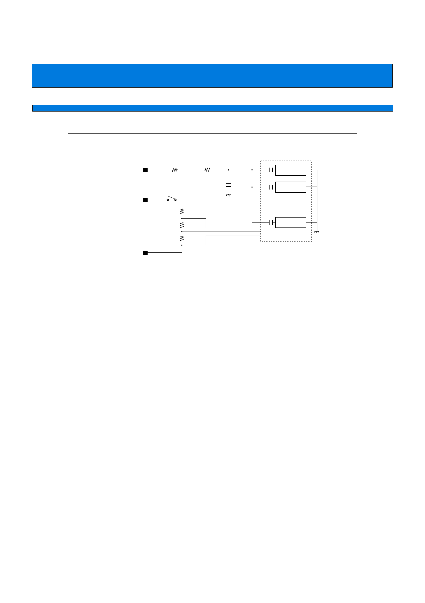
3. Precautions when Using an External Clock
When an external clock is used, drive X0 only and X1 should be left open.
• Using an External Clock
X0
MB90242A
X1
SS
.
4. Power Supply Pins
When there are several V
within the device when the device is designed in order to prevent misoperation, such as latchup. However, all
of those pins must be connected to the power supply and ground externally in order to reduce unnecessary
emissions, prevent misoperation of strobe signals due to an increase in the ground level, and to observe the
total output current standards.
In addition, give a due consideration to the connection in that current supply be connected to V
the lowest possible impedance.
Finally, it is recommended to connect a capacitor of about 0.1 µ F between V
bypass capacitor.
14
CC
and V
SS
pins, those pins that should have the same electric potential are connected
CC
and V
CC
SS
near this device as a
and V
SS
with

To Top / Lineup / Index
MB90242A Series
5. Crystal Oscillation Circuit
Noise in the vicinity of the X0 and X1 pins will cause this device to operate incorrectly. Design the printed circuit
board so that the bypass capacitor connecting X0, X1 and the crystal oscillator (or ceramic oscillator) to ground
is located as close to the device as possible.
In addition, because printed circuit board artwork in which the area around the X0 and X1 pins is surrounded
by ground provides stable operation, such an arrangement is strongly recommended.
6. CLK Pin
ex. 32 MHz
* : In the external bus mode, the P50/CLK pin is initially configured as a CLK output pin.
X1
X0
Divide by 2 circuit
P50/CLK*
STOP
P50 output
P50 input
7. Cautions in Applying Power Supply
Hold the HST
When the RST pin is in the “L” level, do not hold the HST pin to “L” level.
pin to the “H” level when applying power supply.
to internal blocks
CLK output
15

MB90242A Series
BLOCK DIAGRAM
To Top / Lineup / Index
■
SCK0
SID0
SOD0
SCK1
SID1
SOD1
CC
AV
AVRH
AVRL
SS
AV
AN0 to AN3
AN6
AN7
ATG
TIN0, TIN1
TOT0, TOT1
3
UART
Simple serial
11
2
2
A/D converter
Multiply/accumulate
module
16-bit
timer × 3
MC-16F bus
2
F
16-bit timer
ICU × 4
I/O port × 38
External bus interface
2
MC-16F
F
CPU
63
16
24
4
ASR0 to ASR3
P00 to P07
P10 to P17
P20 to P27
P30 to P37
P40 to P47
P50 to P57
P60 to P63,
P66, P67,
P70 to P75
P80 to P82
D00 to D15
A00 to A23
CLK
RDY
HAK
4
HRQ
WRH
WRL
RD
16
INT0 to INT3
X0
X1
RST
HST
MD2 to MD0
RAM
4
External interrupt
timer × 4
7
Clock controller

ELECTRICAL CHARACTERISTICS
1. Absolute Maximum Ratings
To Top / Lineup / Index
MB90242A Series
■
SS
(V
= AV
Value
Parameter
Symbol
Unit Remarks
Min. Max.
CC VSS – 0.3 VSS + 7.0 V
V
Power supply voltage
AVCC VCC – 0.3 VCC + 7.0 V
Input voltage VI*VSS – 0.3 VCC + 0.3 V
Output voltage VO*VSS – 0.3 VCC + 0.3 V
“L” level output current IOL 10 mA
“L” level average output current IOLAV 4mA
“L” level total average output current ΣIOLAV 50 mA
“H” level output current IOH –10 mA
“H” level average output current IOHAV –4 mA
“H” level total average output current ΣIOHAV –48 mA
Power consumption PD 600 mW
Operating temperature TA –30 +70 °C
Storage temperature Tstg –55 +150 °C
* :V
and V
I
must not exceed V
O
+ 0.3 V.
CC
SS
= 0.0 V)
WARNING: Semiconductor devices can be permanently damaged by application of stress (voltage, current,
temperature, etc.) in excess of absolute maximum ratings. Do not exceed these ratings.
2. Recommended Operating Conditions
(VSS = AVSS = 0.0 V)
Parameter
Power supply voltage V
Operating temperature T
Symbol
CC
A –30 +70 °C External bus mode
WARNING: Recommended operating conditions are normal operating ranges for the semiconductor device. All
the device’s electrical characteristics are warranted when operated within these ranges.
Always use semiconductor de vices within the recommended operating conditions . Operation outside
these ranges may adversely affect reliability and could result in device failure.
No warranty is made with respect to uses, operating conditions, or combinations not represented on
the data sheet. Users considering application outside the listed conditions are advised to contact their
FUJITSU representative beforehand.
Value
Min. Max.
4.5
2.0
5.5
5.5
Unit Remarks
V
V
For retaining RAM data in the stop
mode
17

To Top / Lineup / Index
MB90242A Series
3. DC Characteristics
(VCC = 5.0 V ±10%, VSS = AVSS = 0.0 V, TA = –30°C to +70°C)
Parameter Symbol Pin name Condition
IH1 — — 0.7 VCC — VCC + 0.3 V CMOS input
V
“H” level input
voltage
“L” level input
voltage
“H” level output
voltage
“L” level output
voltage
“H” level input
current
“L” level input
current
Pull-up resistor RPULL RST VCC = 5.0 V 22 — 110 kΩ
Power supply
current
Input capacitance CIN
Open-drain
output leakage
current
VIH2 — — 2.2 — VCC + 0.3 V TTL input
VIHIS — — 0.8 VCC — VCC + 0.3 V Hysteresis input
VIHM MD0 to MD2 — VCC – 0.3 — VCC + 0.3 V
VIL1 ——VSS – 0.3 — 0.3 VCC V CMOS input
VIL2 ——VSS – 0.3 — 0.8 V TTL input
VILIS ——VSS – 0.3 — 0.2 VCC V Hysteresis input
VILM MD0 to MD2 — VSS – 0.3 — VSS + 0.3 V
All ports except
VOH
P60 to P63,
P66, P67
VOL All ports
IIH1 Except RST
IIH2 —
IIH3 —
IIL1 Except RST
IIL2 —
IIL3 —
ICC VCC
ICCS VCC
ICCH VCC
Except VCC,
VSS
P60 to P63,
ILEAK
P66, P67
VCC = 4.5 V
IOH = –4.0 mA
VCC = 4.5 V
IOL = 4.0 mA
VCC = 5.5 V
VIH = 0.7 VCC
VCC = 5.5 V
VIH = 2.2 V
VCC = 5.5 V
VIH = 0.8 VCC
VCC = 5.5 V
VIL = 0.3 VCC
VCC = 5.5 V
VIL = 0.8 VCC
VCC = 5.5 V
VIL = 0.2 VCC
VCC = 5.0 V ±10%
FC = 32 MHz
VCC = 5.0 V ±10%
FC = 32 MHz
In sleep mode
VCC = 5.0 V ±10%
TA = +25°C
In stop mode
— — 10 — pF
— — 0.1 10 µA
Min. Typ. Max.
VCC – 0.5 ——V
— — 0.4 V
— — –10 µA CMOS input
— — –10 µA TTL input
— — –10 µA Hysteresis input
——10µA CMOS input
——10µA TTL input
——10µAHysteresis input
— 80 100 mA
—3050mA
— 0.1 10 µA
Value
Unit Remarks
In operation
mode
18

4. AC Characteristics
(1) Clock Timing
Parameter
Clock frequency F
Clock cycle time tC
Input clock pulse width
Input clock rising/
falling time
Symbol
C
PWH
PWL
tCR
tCF
To Top / Lineup / Index
MB90242A Series
CC = 5.0 V ±10%, VSS = 0.0 V, TA = –30°C to +70°C)
(V
Pin
name
X0
X1
X0
X1
Condition
— — 32 MHz
— 1/FC —ns
X0 — 10 — ns
X0 — — 8 ns
Value
Unit Remarks
Min. Max.
• Clock Timing
tC
PWH
tCF
PWL
• Relationship between Clock Frequency and Supply Voltage
VCC
[V]
5.5
Operating garantee range
A = –30°C to +70°C, external bus mode)
(T
0.7 VCC
0.3 VCC
tCR
4.5
0
32
FC
[MHz]
19

To Top / Lineup / Index
MB90242A Series
(2) Clock Output Timing
(VCC = 5.0 V ±10%, VSS = 0.0 V, TA = –30°C to +70°C)
Parameter
Machine cycle time t
Symbol Pin name Condition
CYC CLK — tC × 2 — ns
CLK ↑ → CLK↓ tCHCL CLK — tCYC/2 – 20 tCYC/2 ns
tCYC
tCHCL
Value
Min. Max.
Unit Remarks
CLK
(3) Reset and Hardware Standby Input
(V
CC = 5.0 V ±10%, VSS = 0.0 V, TA = –30°C to +70°C)
Value
Parameter
Reset input time t
Symbol Pin name Condition
Min. Max.
RSTL RST —tCYC × 5—ns
Unit Remarks
Hardware standby input time tHSTL HST —tCYC × 5—ns
Note: The machine cycle time (tCYC) at hardware standby is set to 1/32 divided oscillation.
tRSTL, tHSTL
RST
HST
20

To Top / Lineup / Index
MB90242A Series
(4) Power-on Reset
(VCC = 5.0 V ±10%, VSS = 0.0 V, TA = –30°C to +70°C)
Parameter
Power supply rising time t
Symbol Pin name Condition
R VCC — — 30 ms
Power supply cut-off time tOFF VCC —1—ms
Note: The above standards are the values needed in order to activate a power-on reset.
tR
Value
Unit Remarks
Min. Max.
VCC must be lower
than 0.2 V before
power is applied.
VCC
If power supply voltage needs to be changed in the course of operation, a smooth voltage rise is
recommended by suppressing the voltage variation as shown below.
5.0 V
CC 2.0 V
V
V
SS
+2.97 V
+0.2 V
Holding RAM data
tOFF
It is recommended that the rate of
increase in the voltage be kept to
no more that 50 mV/ms.
21

To Top / Lineup / Index
MB90242A Series
(5) Bus Read Timing
(VCC = 5.0 V ±10%, VSS = 0.0 V, TA = –30°C to +70°C)
Parameter
Address cycle time t
Symbol Pin name Condition
ACYC Address — 2 tCYC – 10 — ns
Valid address → RD ↓ time tAVRL Address — tCYC/2 – 15 — ns
RD pulse width tRLRH RD —tCYC – 25 — ns
RD ↓ → Valid data input tRLDV
RD ↑ → data hold time tRHDX —0—ns
D00 to D15
——tCYC/ – 30 ns
Valid address → Valid data input tAVDV ——3 tCYC/2 – 40 ns
RD ↑ → Address valid time tRHAX Address — tCYC/2 – 20 — ns
Valid address → CLK ↑ time tAVCH
Address
CLK
—tCYC/2 – 25 — ns
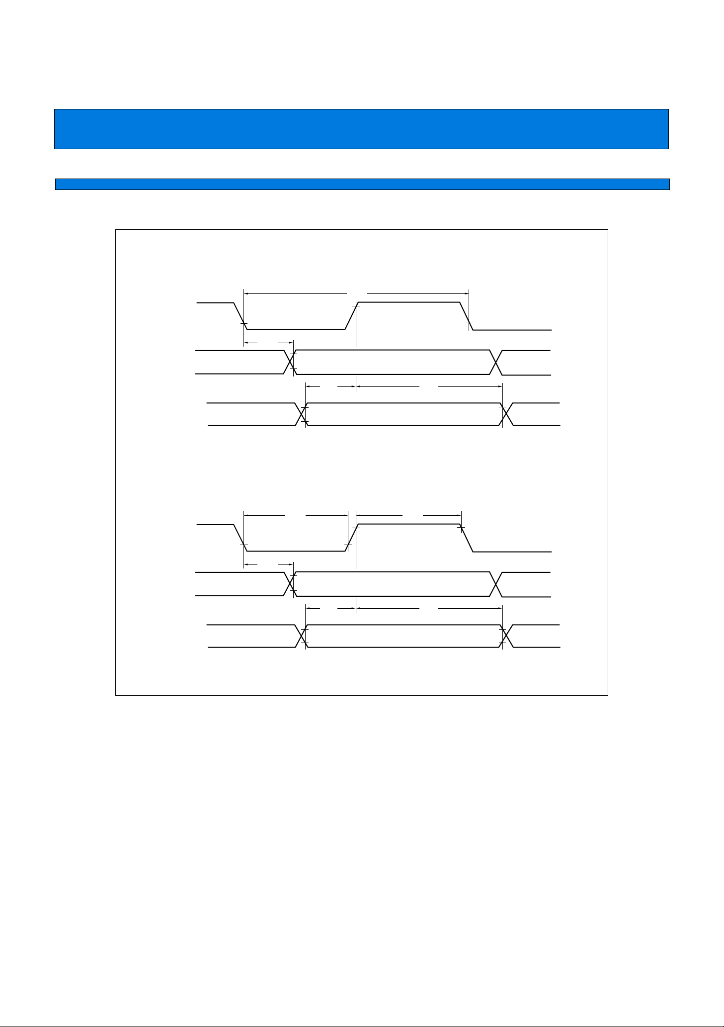
RD ↓ → CLK ↓ time tRLCL RD, CLK — tCYC/2 – 25 — ns
Value
Unit Remarks
Min. Max.
tAVCH tRLCL
CLK
RD
Address
Data
tAVRL tRLRH
tACYC
tRLDV
tAVDV
tRHDX
tRHAX
2.2 VCC
0.8 V
CC
22

To Top / Lineup / Index
MB90242A Series
(6) Bus Write Timing
(VCC = 5.0 V ±10%, VSS = 0.0 V, TA = –30°C to +70°C)
Parameter
Valid address → WR
↓ time tAVWL Address — tCYC/2 – 15 — ns
Symbol Pin name Condition
WR pulse width tWLWH WRL, WRH —tCYC – 25 — ns
Write data → WR ↑ time tDVWH D00 to D15 — tCYC – 40 — ns
WR ↑ → Data hold time tWHDX D00 to D15 — tCYC/2 – 15 — ns
WR ↑ → Address invalid time tWHAX Address — tCYC/2 – 15 — ns
WR ↓ → CLK ↑ time tWLCL
WRL, WRH,
CLK
—tCYC/2 – 25 — ns
Value
Unit Remarks
Min. Max.
CLK
WR
(WRL, WRH)
Address
Data
tWLCL
tAVWL tWLWH
tDVWH tWHDX
Write data
tWHAX
0.8 VCC
2.2 VCC
23

To Top / Lineup / Index
MB90242A Series
(7) Ready Input Timing
(VCC = 5.0 V ±10%, VSS = 0.0 V, TA = –30°C to +70°C)
Parameter
RDY setup time t
Symbol Pin name Condition
RYHS RDY
At 32 MHz oscillation
RDY hold time tRYHH RDY 0 60 ns
Note: If the setup time of RDY on a falling edge is insufficient, use the auto ready function.
CLK
Value
Min. Max.
15 60 ns
Unit Remarks
RD/WR
RDY
A23 to A00
D15 to D00
D15 to D00
tRYHH
tRYHS
External address
Wait cycle
Read data
Wait cycle
Write data
24

To Top / Lineup / Index
MB90242A Series
(8) Hold Timing
(VCC = 5.0 V ±10%, VSS = 0.0 V, TA = –30°C to +70°C)
Parameter
Pin floating → HAK
HAK ↑ time → Pin valid time tHAHV HAK —tCYC 2 tCYC ns
↓ time tXHAL HAK —30tCYC ns
Symbol Pin name Condition
Value
Unit Remarks
Min. Max.
Note: At least one cycle is required from the time when HRQ is fetched until HAK
HRQ
HAK
tXHAL
Each pin
High impedance
tHAHV
changes.
25

To Top / Lineup / Index
MB90242A Series
(9) UART Timing
(VCC = 5.0 V ±10%, VSS = 0.0 V , TA = –30°C to +70°C)
Parameter
Serial clock cycle time t
SCK ↓ → SOD delay
time
Valid SID → SCK ↑ tIVSH — — 100 — ns
SCK ↑ → Valid
SID hold time
Serial clock “H” pulse
width
Serial clock “L” pulse
width
SCK ↓ → SOD delay
time
Valid SID → SCK ↑ tIVSH — — 60 — ns
SCK ↑ → Valid SID
hold time
Symbol Pin name Condition
SCYC — — 8 tCYC —ns
tSLOV — — –80 80 ns
tSHIX — — 60 — ns
tSHSL — — 4 tCYC —ns
tSLSH — — 4 tCYC —ns
tSLOV — — — 150 ns
tSHIX — — 60 — ns
Value
Min. Max.
Unit Remarks
For internal
shift clock
mode output
pin,
CL = 80 pF
For external
shift clock
mode output
pin,
CL = 80 pF
Notes:
• These are the AC characteristics for CLK synchronous mode.
• CL is the load capacitance added to pins during testing.
• tCYC is the machine cycle time (unit: ns).
26
• Internal Shift Clock Mode
SCK0
SOD0
SID0
To Top / Lineup / Index
MB90242A Series
tSCYC
tSLOV
tIVSH tSHIX
• External Shift Clock Mode
SCK0
SOD0
SID0
tSLSH tSHSL
tSLOV
tIVSH tSHIX
27

To Top / Lineup / Index
MB90242A Series
(10) Simple Serial Timing
(VCC = 5.0 V ±10%, VSS = 0.0 V , TA = –30°C to +70°C)
Parameter
Serial clock cycle time t
Symbol Pin name Condition
SCYC — — 2 tCYC —ns
SCK ↓ → SOD delay time tSLOV ———tCYC/2 ns
Valid SID → SCK ↑ tIVSH — — 1 tCYC —ns
SCK ↑ → Valid SID hold time tSHIX — — 1 tCYC —ns
Value
Unit Remarks
Min. Max.
For operation
output pin,
CL = 80 pF
Notes: • C
L is the load capacitance added to pins during testing.
• tCYC is the machine cycle time (unit: ns).
• Internal Shift Clock Mode
SCK1
SOD1
SID1
(11) Timer Input Timing
Parameter
Input pulse width
tSCYC
tSLOV
tIVSH tSHIX
CC = 5.0 V ±10%, VSS = 0.0 V , TA = –30°C to +70°C)
(V
Symbol Pin name Condition
TIWH
t
tTIWL
ASR0 to ASR3,
TIN0 to TIN2
—4 tCYC —ns
Value
Unit Remarks
Min. Max.
28
ASR0 to ASR3
TIN0 to TIN2
tTIWH tTIWL

(12) Timer Ouput Timing
Parameter
SCK ↑ → Change time t
To Top / Lineup / Index
MB90242A Series
(V
CC = 5.0 V ±10%, VSS = 0.0 V , TA = –30°C to +70°C)
Symbol Pin name Condition
TO TOT0, T OT1 VCC = 5.0 V ±10% — 40 ns
CLK
TOT0, TOT1
Value
Unit Remarks
Min. Max.
(13) Trigger Input Timing
Parameter
Input pulse width
ATG
INT0 to INT3
t
TO
(V
CC = 5.0 V ±10%, VSS = 0.0 V , TA = –30°C to +70°C)
Symbol Pin name Condition
TRGH
t
tTRGL
ATG,
INT0 to INT3
—5 tCYC —ns
Value
Unit Remarks
Min. Max.
tTRGLtTRGH
29

To Top / Lineup / Index
MB90242A Series
5. A/D Converter Electrical Characteristics
(VCC = 5.0 V ±10%, VSS = 0.0 V , TA = –30°C to +70°C)
Parameter
Symbol Pin name
Min. Typ. Max.
Resolution — — — 8, 10 10 bit
Total error — — — — ±3.0 LSB
Linearity error — — — — ±2.0 LSB
Differential linearity error — — — — ±1.9 LSB
Zero transition voltage V
Full-scale transition
voltage
VFST
Ot
AN6, AN7
AN0 to AN3
AN6, AN7
AVRL – 1.0 AVRL + 1.0 AVRL + 3.0 LSB
AVRH – 4.0 AVRH – 1.0 AVRH + 1.0 LSB
AN0 to AN3
Conversion time — — 1.25 — — µs
Sampling period — — 560 — — ns
Conversion period a — — 125 — — ns
Conversion period b — — 125 — — ns
Conversion period c — — 250 — — ns
Value
Unit Remarks
Specified by the
ADCT register
settings.*
1
VCC = 5.0 V±10%
Analog port input current I
Analog input voltage —
AIN
AN0 to AN3
AN6, AN7
AN0 to AN3
AN6, AN7
— 0.1 3 µA
AVRL — AVRH V
— AVRH AVRL + 2.7 —AVCC V
Reference voltage
— AVRL 0 — AVRH – 2.7 V
Power supply current
Reference voltage
supply current
Interchannel disparity —
*1: When F
C = 32 MHz, and the machine cycle is 62.5 ns.
IA
AVCC
2
AS*
I
IR
AVRH
2
RS*
I
AN0 to AN3
AN6, AN7
—1520mA
—— 5µA
— 1.5 2 mA
—— 5µA
— — 4 LSB
*2: IAS and IRS are current when the A/D converter is not operating and the CPU is stopped.
Notes: • The smaller | AVRH – AVRL |, the greater the error would become relatively.
• If the output impedance of the external circuit of an analog input is too high, an analog voltage sampling
time might be insufficient. When the sampling period close to the minimum value is used, the output
impedance of the external circuit should be less than approximately 300 Ω.
AVRH – AVRL ≥ 2.7
AVCC = 5.5 V
in stop mode
AVCC = 5.5 V
in stop mode
30
• Analog Input Circuit Model Diagram
To Top / Lineup / Index
MB90242A Series
C0 Approx. 60 pF
Analog input pin
AVRH
AVRL
Note: Use the values shown as guides only.
RON1
Approx. 300 Ω
Switched on only during
A/D conversion.
Approx. 150 Ω
R
ON2
Approx.
4 pF
1
C
Comparator
Comparator
.
.
Comparator
31

To Top / Lineup / Index
MB90242A Series
6. A/D Converter Glossary
• Resolution
Analog changes that are identifiable with the A/D converter.
If the resolution is 10 bits, the analog voltage can be resolved into 2
• Total error
The difference between theoretical and actual conv ersion values caused b y the zero transition error , full-scale
transition error, non-linearity error, differential linearity error, and noise.
• Linearity error
The deviation of the straight line connecting the zero transition point (“00 0000 0000” ↔ “00 0000 0001”) with
the full-scale transition point (“11 1111 1110” ↔ “11 1111 1111”) from actual conversion characteristics.
• Differential linearity error
The deviation of input voltage needed to change the output by 1 LSB from the theoretical value.
Digital output
11 1111 1111
11 1111 1110
•
•
•
•
•
•
•
•
•
•
•
•
11 1111 1110
00 0000 0001
00 0000 0000
(1 LSB × N + V
VOT
VNT
OT)
V(N+1)T
10
.
Linearity error
V
FST
32
• 1 LSB =
• Linearity error = (LSB)
• Differential linearity error = –1 (LSB)
VFST – VOT
1022
NT – (1 LSB × N + VOT)
V
1 LSB
(N+1)T – VNT
V
1 LSB

To Top / Lineup / Index
MB90242A Series
■ INSTRUCTION SET (412 INSTRUCTIONS)
Table 1 Explanation of Items in Table of Instructions
Item Explanation
Mnemonic Upper-case letters and symbols: Represented as they appear in assembler
Lower-case letters: Replaced when described in assembler.
Numbers after lower-case letters: Indicate the bit width within the instruction.
# Indicates the number of bytes.
~ Indicates the number of cycles.
See Table 4 for details about meanings of letters in items.
B Indicates the correction value for calculating the number of actual cycles during
execution of instruction.
The number of actual cycles during execution of instruction is summed with the value in
the “cycles” column.
Operation Indicates operation of instruction.
LH Indicates special operations involving the bits 15 through 08 of the accumulator.
Z: Transf ers “0”.
X: Extends before transferring.
—: Transf ers nothing.
AH Indicates special operations involving the high-order 16 bits in the accumulator.
*: Transfers from AL to AH.
—: No transfer.
Z: Transf ers 00
X: Transf ers 00H or FFH to AH by extending AL.
I Indicates the status of each of the following flags: I (interrupt enable), S (stack), T (sticky
S
T
N
Z
V
C
RMW Indicates whether the instruction is a read-modify-write instruction (a single instruction
bit), N (negative), Z (zero), V (overflow), and C (carry).
*: Changes due to execution of instruction.
—: No change.
S: Set by execution of instruction.
R: Reset by execution of instruction.
that reads data from memory, etc., processes the data, and then writes the result to
memory.).
*: Instruction is a read-modify-write instruction
—: Instruction is not a read-modify-write instruction
Note: Cannot be used for addresses that have different meanings depending on
whether they are read or written.
H to AH.
33

MB90242A Series
Table 2 Explanation of Symbols in Table of Instructions
Symbol Explanation
A 32-bit accumulator
The number of bits used varies according to the instruction.
Byte: Low order 8 bits of AL
Word: 16 bits of AL
Long: 32 bits of AL, AH
AH High-order 16 bits of A
AL Low-order 16 bits of A
SP Stack pointer (USP or SSP)
PC Program counter
SPCU Stack pointer upper limit register
SPCL Stack pointer lower limit register
PCB Program bank register
DTB Data bank register
ADB Additional data bank register
SSB System stack bank register
USB User stack bank register
SPB Current stack bank register (SSB or USB)
DPR Direct page register
brg1 DTB, ADB, SSB, USB, DPR, PCB, SPB
brg2 DTB, ADB, SSB, USB, DPR, SPB
Ri R0, R1, R2, R3, R4, R5, R6, R7
RWi RW0, RW1, RW2, RW3, RW4, RW5, RW6, RW7
RWj RW0, RW1, RW2, RW3
RLi RL0, RL1, RL2, RL3
dir
addr16
addr24
addr24 0 to 15
addr24 16 to 23
io I/O area (000000
Compact direct addressing
Direct addressing
Physical direct addressing
Bits 0 to 15 of addr24
Bits 16 to 23 of addr24
To Top / Lineup / Index
H to 0000FFH)
34
(Continued)

(Continued)
Symbol Explanation
#imm4
#imm8
#imm16
#imm32
ext (imm8)
disp8
disp16
bp Bit offset value
vct4
vct8
( )b Bit address
rel
ear
eam
rlst Register list
To Top / Lineup / Index
MB90242A Series
4-bit immediate data
8-bit immediate data
16-bit immediate data
32-bit immediate data
16-bit data signed and extended from 8-bit immediate data
8-bit displacement
16-bit displacement
Vector number (0 to 15)
Vector number (0 to 255)
Branch specification relative to PC
Effective addressing (codes 00 to 07)
Effective addressing (codes 08 to 1F)
35

MB90242A Series
To Top / Lineup / Index
Table 3 Effective Address Fields
Code Notation Address format
00
01
02
03
04
05
06
07
08
09
0A
0B
0C
0D
0E
0F
10
11
12
13
14
15
16
17
18
19
1A
1B
1C
1D
1E
1F
R0
R1
R2
R3
R4
R5
R6
R7
RW0
RW1
RW2
RW3
RW4
RW5
RW6
RW7
@RW0
@RW1
@RW2
@RW3
@RW0 +
@RW1 +
@RW2 +
@RW3 +
@RW0 + disp8
@RW1 + disp8
@RW2 + disp8
@RW3 + disp8
@RW4 + disp8
@RW5 + disp8
@RW6 + disp8
@RW7 + disp8
@RW0 + disp16
@RW1 + disp16
@RW2 + disp16
@RW3 + disp16
@RW0 + RW7
@RW1 + RW7
@PC + dip16
addr16
RL0
(RL0)
RL1
(RL1)
RL2
(RL2)
RL3
(RL3)
Register direct
“ea” corresponds to byte, word, and
long-word types, starting from the
left
Register indirect 0
Register indirect with post-increment 0
Register indirect with 8-bit
displacement
Register indirect with 16-bit
displacemen
Register indirect with index
Register indirect with index
PC indirect with 16-bit displacement
Direct address
Number of bytes in
address extemsion*
—
1
2
0
0
2
2
* :The number of bytes for address extension is indicated by the “+” symbol in the “#” (number of bytes) column in
the Table of Instructions.
36

To Top / Lineup / Index
MB90242A Series
Table 4 Number of Execution Cycles for Each Form of Addressing
Code Operand
00 to 07 Ri
RWi
RLi
08 to 0B @RWj 1
0C to 0F @RWj + 4
10 to 17 @RWi + disp8 1
18 to 1B @RWj + disp16 1
1C
1D
1E
1F
* :“(a)” is used in the “cycles” (number of cycles) column and column B (correction value) in the Table of Instructions.
Table 5 Correction Values for Number of Cycles Used to Calculate Number of Actual Cycles
Operand
Internal register + 0 + 0 + 0
Internal RAM even address + 0 + 0 + 0
Internal RAM odd address + 0 + 1 + 2
Even address not in internal RAM + 1 + 1 + 2
Odd address not in internal RAM + 1 + 3 + 6
External data bus (8 bits) + 1 + 3 + 6
@RW0 + RW7
@RW1 + RW7
@PC + dip16
@addr16
Number of execution cycles for each from of addressing
Listed in Table of Instructions
(b)* (c)* (d)*
byte word long
(a)*
2
2
2
1
* :“(b)”, “(c)”, and “(d)” are used in the “cycles” (number of cycles) column and column B (correction value) in the
Table of Instructions.
37

MB90242A Series
Table 6 Transfer Instructions (Byte) [50 Instructions]
Mnemonic # cycles B Operation LH AH I S T N Z V C RMW
MOV A, dir
MOV A, addr16
MOV A, Ri
MOV A, ear
MOV A, eam
MOV A, io
MOV A, #imm8
MOV A, @A
MOV A, @RLi+disp8
MOV A, @SP+disp8
MOVP A, addr24
MOVP A, @A
MOVN A, #imm4
2
3
1
2
2+
2
2
2
3
3
5
2
1
2
2
1
1
2+ (a)
2
2
2
6
3
3
2
1
(b)
byte (A) ← (dir)
(b)
byte (A) ← (addr16)
0
byte (A) ← (Ri)
0
byte (A) ← (ear)
(b)
byte (A) ← (eam)
(b)
byte (A) ← (io)
0
byte (A) ← imm8
(b)
byte (A) ← ((A))
(b)
byte (A) ← ((RLi))+disp8)
(b)
byte (A) ← ((SP)+disp8)
(b)
byte (A) ←(addr24)
(b)
byte (A) ← ((A))
0
byte (A) ← imm4
To Top / Lineup / Index
Z
*
–
–
–
*
*
–
–
–
Z
*
–
–
–
*
*
–
–
–
Z
*
–
–
–
*
*
–
–
–
Z
*
–
–
–
*
*
–
–
–
Z
*
–
–
–
*
*
–
–
–
Z
*
–
–
–
*
*
–
–
–
Z
*
–
–
–
*
*
–
–
–
Z
–
–
–
–
*
*
–
–
–
Z
*
–
–
–
*
*
–
–
–
Z
*
–
–
–
*
*
–
–
–
Z
*
–
–
–
*
*
–
–
–
Z
–
–
–
–
*
*
–
–
–
Z
*
–
–
–
R
*
–
–
–
MOVX A, dir
MOVX A, addr16
MOVX A, Ri
MOVX A, ear
MOVX A, eam
MOVX A, io
MOVX A, #imm8
MOVX A, @A
MOVX A,@RWi+disp8
MOVX A, @RLi+disp8
MOVX A, @SP+disp8
MOVPXA, addr24
MOVPXA, @A
MOV dir, A
MOV addr16, A
MOV Ri, A
MOV ear, A
MOV eam, A
MOV io, A
MOV @RLi+disp8, A
MOV @SP+disp8, A
MOVP addr24, A
MOV Ri, ear
MOV Ri, eam
MOVP @A, Ri
MOV ear, Ri
MOV eam, Ri
MOV Ri, #imm8
MOV io, #imm8
MOV dir, #imm8
MOV ear, #imm8
MOV eam, #imm8
2
3
2
2
2+
2
2
2
2
3
3
5
2
2
3
1
2
2+
2
3
3
5
2
2+
2
2
2+
2
3
3
3
3+
2
2
1
1
2+ (a)
2
2
2
3
6
3
3
2
2
2
1
2
2+ (a)
2
6
3
3
2
3+ (a)
3
3
3+ (a)
2
3
3
2
2+ (a)
(b)
byte (A) ← (dir)
(b)
byte (A) ← (addr16)
0
byte (A) ← (Ri)
0
byte (A) ← (ear)
(b)
byte (A) ← (eam)
(b)
byte (A) ← (io)
0
byte (A) ← imm8
(b)
byte (A) ← ((A))
(b)
byte (A) ← ((RWi))+disp8)
(b)
byte (A) ← ((RLi))+disp8)
(b)
byte (A) ← ((SP)+disp8)
(b)
byte (A) ←(addr24)
(b)
byte (A) ← ((A))
(b)
byte (dir) ← (A)
(b)
byte (addr16) ← (A)
0
byte (Ri) ← (A)
0
byte (ear) ← (A)
(b)
byte (eam) ← (A)
(b)
byte (io) ← (A)
(b)
byte ((RLi)) +disp8) ← (A)
(b)
byte ((SP)+disp8) ← (A)
(b)
byte (addr24) ← (A)
0
byte (Ri) ← (ear)
(b)
byte (Ri) ← (eam)
(b)
byte ((A)) ← (Ri)
0
byte (ear) ← (Ri)
(b)
byte (eam) ← (Ri)
0
byte (Ri) ← imm8
(b)
byte (io) ← imm8
(b)
byte (dir) ← imm8
0
byte (ear) ← imm8
(b)
byte (eam) ← imm8
X
*
–
–
–
*
*
–
–
–
X
*
–
–
–
*
*
–
–
–
X
*
–
–
–
*
*
–
–
–
X
*
–
–
–
*
*
–
–
–
X
*
–
–
–
*
*
–
–
–
X
*
–
–
–
*
*
–
–
–
X
*
–
–
–
*
*
–
–
–
X
–
–
–
–
*
*
–
–
–
X
*
–
–
–
*
*
–
–
–
X
*
–
–
–
*
*
–
–
–
X
*
–
–
–
*
*
–
–
–
X
*
–
–
–
*
*
–
–
–
X
–
–
–
–
*
*
–
–
–
–
–
–
–
–
*
*
–
–
–
–
–
–
–
–
*
*
–
–
–
–
–
–
–
–
*
*
–
–
–
–
–
–
–
–
*
*
–
–
–
–
–
–
–
–
*
*
–
–
–
–
–
–
–
–
*
*
–
–
–
–
–
–
–
–
*
*
–
–
–
–
–
–
–
–
*
*
–
–
–
–
–
–
–
–
*
*
–
–
–
–
–
–
–
–
*
*
–
–
–
–
–
–
–
–
*
*
–
–
–
–
–
–
–
–
*
*
–
–
–
–
–
–
–
–
*
*
–
–
–
–
–
–
–
–
*
*
–
–
–
–
–
–
–
–
*
*
–
–
–
–
–
–
–
–
–
–
–
–
–
–
–
–
–
–
–
–
–
–
–
–
–
–
–
–
*
*
–
–
–
–
–
–
–
–
–
–
–
–
–
MOV @AL, AH
38
2
2
(b)
byte ((A)) ← (AH)
–
–
–
–
–
*
*
–
–
–
(Continued)

To Top / Lineup / Index
MB90242A Series
(Continued)
Mnemonic # cycles B Operation LH AH I S T N Z V C RMW
XCH A, ear
XCH A, eam
XCH Ri, ear
XCH Ri, eam
For an explanation of “(a)” and “(b)”, refer to Table 4, “Number of Execution Cycles for Each Form of Addressing,”
and Table 5, “Correction Values for Number of Cycles Used to Calculate Number of Actual Cycles.”
2
2+
2
2+
3
3+ (a)
4
5+ (a)
0
2× (b)
0
2× (b)
byte (A) ↔ (ear)
byte (A) ↔ (eam)
byte (Ri) ↔ (ear)
byte (Ri) ↔ (eam)
Z
–
–
–
–
–
–
–
–
–
Z
–
–
–
–
–
–
–
–
–
–
–
–
–
–
–
–
–
–
–
–
–
–
–
–
–
–
–
–
–
39

MB90242A Series
Table 7 Transfer Instructions (Word) [40 Instructions]
Mnemonic # cycles B Operation LH AH I S T N Z V C RMW
MOVW A, dir
MOVW A, addr16
MOVW A, SP
MOVW A, RWi
MOVW A, ear
MOVW A, eam
MOVW A, io
MOVW A, @A
MOVW A, #imm16
MOVW A, @RWi+disp8
MOVW A, @RLi+disp8
MOVW A, @SP+disp8
MOVPW A, addr24
MOVPW A, @A
MOVW dir, A
MOVW addr16, A
MOVW SP, # imm16
MOVW SP, A
MOVW RWi, A
MOVW ear, A
MOVW eam, A
MOVW io, A
MOVW @RWi+disp8, A
MOVW @RLi+disp8, A
MOVW @SP+disp8, A
MOVPW addr24, A
MOVPW @A, RWi
MOVW RWi, ear
MOVW RWi, eam
MOVW ear, RWi
MOVW eam, RWi
MOVW RWi, #imm16
MOVW io, #imm16
MOVW ear, #imm16
MOVW eam, #imm16
2
3
1
1
2
2+
2
2
3
2
3
3
5
2
2
3
4
1
1
2
2+
2
2
3
3
5
2
2
2+
2
2+
3
4
4
4+
2
2
2
1
1
2+ (a)
2
2
2
3
6
3
3
2
2
2
2
2
1
2
2+ (a)
2
3
6
3
3
3
2
3+ (a)
3
3+ (a)
2
3
2
2+ (a)
(c)
word (A) ← (dir)
(c)
word (A) ← (addr16)
0
word (A) ← (SP)
0
word (A) ← (RWi)
0
word (A) ← (ear)
(c)
word (A) ← (eam)
(c)
word (A) ← (io)
(c)
word (A) ← ((A))
0
word (A) ← imm16
(c)
word (A) ← ((RWi) +disp8)
(c)
word (A) ← ((RLi) +disp8)
(c)
word (A) ← ((SP) +disp8
(c)
word (A) ← (addr24)
(c)
word (A) ← ((A))
(c)
word (dir) ← (A)
(c)
word (addr16) ← (A)
0
word (SP) ← imm16
0
word (SP) ← (A)
0
word (RWi) ← (A)
0
word (ear) ← (A)
(c)
word (eam) ← (A)
(c)
word (io) ← (A)
(c)
word ((RWi) +disp8) ← (A)
(c)
word ((RLi) +disp8) ← (A)
(c)
word ((SP) +disp8) ← (A)
(c)
word (addr24) ← (A)
(c)
word ((A)) ← (RWi)
0
word (RWi) ← (ear)
(c)
word (RWi) ← (eam)
0
word (ear) ← (RWi)
(c)
word (eam) ← (RWi)
0
word (RWi) ← imm16
(c)
word (io) ← imm16
0
word (ear) ← imm16
(c)
word (eam) ← imm16
To Top / Lineup / Index
–
*
–
–
–
*
*
–
–
–
–
*
–
–
–
*
*
–
–
–
–
*
–
–
–
*
*
–
–
–
–
*
–
–
–
*
*
–
–
–
–
*
–
–
–
*
*
–
–
–
–
*
–
–
–
*
*
–
–
–
–
*
–
–
–
*
*
–
–
–
–
–
–
–
–
*
*
–
–
–
–
*
–
–
–
*
*
–
–
–
–
*
–
–
–
*
*
–
–
–
–
*
–
–
–
*
*
–
–
–
–
*
–
–
–
*
*
–
–
–
–
*
–
–
–
*
*
–
–
–
–
–
–
–
–
*
*
–
–
–
–
–
–
–
–
*
*
–
–
–
–
–
–
–
–
*
*
–
–
–
–
–
–
–
–
*
*
–
–
–
–
–
–
–
–
*
*
–
–
–
–
–
–
–
–
*
*
–
–
–
–
–
–
–
–
*
*
–
–
–
–
–
–
–
–
*
*
–
–
–
–
–
–
–
–
*
*
–
–
–
–
–
–
–
–
*
*
–
–
–
–
–
–
–
–
*
*
–
–
–
–
–
–
–
–
*
*
–
–
–
–
–
–
–
–
*
*
–
–
–
–
–
–
–
–
*
*
–
–
–
–
–
–
–
–
*
*
–
–
–
–
–
–
–
–
*
*
–
–
–
–
–
–
–
–
*
*
–
–
–
–
–
–
–
–
*
*
–
–
–
–
–
–
–
–
*
*
–
–
–
–
–
–
–
–
–
–
–
–
–
–
–
–
–
–
*
*
–
–
–
–
–
–
–
–
–
–
–
–
–
2
2
(c)
MOVW @AL, AH
2
XCHW A, ear
XCHW A, eam
XCHW RWi, ear
XCHW RWi, eam
Note: For an explanation of “(a)” and “(c)”, refer to Table 4, “Number of Execution Cycles for Each Form of
Addressing,” and Table 5, “Correction Values for Number of Cycles Used to Calculate Number of Actual
Cycles.”
40
2+
2
2+
3
3+ (a)
4
5+ (a)
2× (c)
2× (c)
word ((A)) ← (AH)
0
word (A) ↔ (ear)
word (A) ↔ (eam)
0
word (RWi) ↔ (ear)
word (RWi) ↔ (eam)
–
–
–
–
–
*
*
–
–
–
–
–
–
–
–
–
–
–
–
–
–
–
–
–
–
–
–
–
–
–
–
–
–
–
–
–
–
–
–
–
–
–
–
–
–
–
–
–
–
–

To Top / Lineup / Index
MB90242A Series
Table 8 Transfer Instructions (Long Word) [11 Instructions]
Mnemonic # cycles B Operation LH AH I S T N Z V C RMW
MOVL A, ear
MOVL A, eam
MOVL A, # imm32
MOVL A, @SP + disp8
MOVPL A, addr24
MOVPL A, @A
2
2+
5
3
5
2
1
3+ (a)
3
4
4
3
0
long (A) ← (ear)
(d)
long (A) ← (eam)
0
long (A) ← imm32
(d)
long (A) ← ((SP) +disp8)
(d)
long (A) ← (addr24)
(d)
long (A) ← ((A))
–
–
–
–
–
*
*
–
–
–
–
–
*
*
–
–
–
–
–
*
*
–
–
–
–
–
*
*
–
–
–
–
–
*
*
–
–
–
–
–
*
*
–
–
–
–
–
–
–
–
–
–
–
–
–
–
–
–
–
–
MOVPL @A, RLi
MOVL @SP + disp8, A
MOVPL addr24, A
MOVL ear, A
MOVL eam, A
For an explanation of “(a)” and “(d)”, refer to Table 4, “Number of Execution Cycles for Each Form of Addressing,”
and Table 5, “Correction Values for Number of Cycles Used to Calculate Number of Actual Cycles.”
2
3
5
2
2+
5
4
4
2
3+ (a)
(d)
long ((A)) ← (RLi)
(d)
long ((SP) + disp8) ← (A)
(d)
long (addr24) ← (A)
0
long (ear) ← (A)
(d)
long (eam) ← (A)
–
–
–
–
–
*
*
–
–
–
–
–
–
–
–
*
*
–
–
–
–
–
–
–
–
*
*
–
–
–
–
–
–
–
–
*
*
–
–
–
–
–
–
–
–
*
*
–
–
–
41

To Top / Lineup / Index
MB90242A Series
Table 9 Addition and Subtraction Instructions (Byte/Word/Long Word) [42 Instructions]
Mnemonic # cycles B Operation LH AH I S T N Z V C RMW
ADD A, #imm8
ADD A, dir
ADD A, ear
ADD A, eam
ADD ear, A
ADD eam, A
ADDC A
ADDC A, ear
ADDC A, eam
ADDDC A
2
2
2
2+
2
2+
1
2
2+
1
2
3
2
3+ (a)
2
3+ (a)
2
2
3+ (a)
3
0
(b)
0
(b)
0
2× (b)
0
0
(b)
0
byte (A) ← (A) +imm8
byte (A) ← (A) +(dir)
byte (A) ← (A) +(ear)
byte (A) ← (A) +(eam)
byte (ear) ← (ear) + (A)
byte (eam) ← (eam) + (A)
byte (A) ← (AH) + (AL) + (C)
byte (A) ← (A) + (ear) + (C)
byte (A) ← (A) + (eam) + (C)
byte (A) ← (AH) + (AL) + (C) (Decimal)
Z
–
–
–
–
*
*
Z
–
–
–
–
*
*
Z
–
–
–
–
*
*
Z
–
–
–
–
*
*
–
–
–
–
–
*
*
Z
–
–
–
–
*
*
Z
–
–
–
–
*
*
Z
–
–
–
–
*
*
Z
–
–
–
–
*
*
Z
–
–
–
–
*
*
*
*
–
*
*
–
*
*
–
*
*
–
*
*
*
*
*
*
*
*
–
*
*
–
*
*
–
*
*
–
SUB A, #imm8
SUB A, dir
SUB A, ear
SUB A, eam
SUB ear, A
SUB eam, A
SUBC A
SUBC A, ear
SUBC A, eam
SUBDC A
ADDW A
ADDW A, ear
ADDW A, eam
ADDW A, #imm16
ADDW ear, A
ADDW eam, A
ADDCW A, ear
ADDCW A, eam
SUBW A
SUBW A, ear
SUBW A, eam
SUBW A, #imm16
SUBW ear, A
SUBW eam, A
SUBCW A, ear
SUBCW A, eam
ADDL A, ear
ADDL A, eam
ADDL A, #imm32
2
2
2
2+
2
2+
1
2
2+
1
1
2
2+
3
2
2+
2
2+
1
2
2+
3
2
2+
2
2+
2
2+
5
2
3
2
3+ (a)
2
3+ (a)
2
2
3+ (a)
3
2
2
3+ (a)
2
2
3+ (a)
2
3+ (a)
2
2
3+ (a)
2
2
3+ (a)
2
3+ (a)
5
6+ (a)
4
0
(b)
0
(b)
0
2× (b)
0
0
(b)
0
0
0
(c)
0
0
2× (c)
0
(c)
0
0
(c)
0
0
2× (c)
0
(c)
0
(d)
0
byte (A) ← (A) –imm8
byte (A) ← (A) – (dir)
byte (A) ← (A) – (ear)
byte (A) ← (A) – (eam)
byte (ear) ← (ear) – (A)
byte (eam) ← (eam) – (A)
byte (A) ← (AH) – (AL) – (C)
byte (A) ← (A) – (ear) – (C)
byte (A) ← (A) – (eam) – (C)
byte (A) ← (AH) – (AL) – (C) (Decimal)
word (A) ← (AH) + (AL)
word (A) ← (A) +(ear)
word (A) ← (A) +(eam)
word (A) ← (A) +imm16
word (ear) ← (ear) + (A)
word (eam) ← (eam) + (A)
word (A) ← (A) + (ear) + (C)
word (A) ← (A) + (eam) + (C)
word (A) ← (AH) – (AL)
word (A) ← (A) – (ear)
word (A) ← (A) – (eam)
word (A) ← (A) –imm16
word (ear) ← (ear) – (A)
word (eam) ← (eam) – (A)
word (A) ← (A) – (ear) – (C)
word (A) ← (A) – (eam) – (C)
long (A) ← (A) + (ear)
long (A) ← (A) + (eam)
long (A) ← (A) +imm32
Z
–
–
–
–
*
*
*
*
–
Z
–
–
–
–
*
*
*
*
–
Z
–
–
–
–
*
*
*
*
–
Z
–
–
–
–
*
*
*
*
–
–
–
–
–
–
*
*
*
*
*
–
–
–
–
–
*
*
*
*
*
Z
–
–
–
–
*
*
*
*
–
Z
–
–
–
–
*
*
*
*
–
Z
–
–
–
–
*
*
*
*
–
Z
–
–
–
–
*
*
*
*
–
–
–
–
–
–
*
*
*
*
–
–
–
–
–
–
*
*
*
*
–
–
–
–
–
–
*
*
*
*
–
–
–
–
–
–
*
*
*
*
–
–
–
–
–
–
*
*
*
*
*
–
–
–
–
–
*
*
*
*
*
–
–
–
–
–
*
*
*
*
–
–
–
–
–
–
*
*
*
*
–
–
–
–
–
–
*
*
*
*
–
–
–
–
–
–
*
*
*
*
–
–
–
–
–
–
*
*
*
*
–
–
–
–
–
–
*
*
*
*
–
–
–
–
–
–
*
*
*
*
*
–
–
–
–
–
*
*
*
*
*
–
–
–
–
–
*
*
*
*
–
–
–
–
–
–
*
*
*
*
–
–
–
–
–
–
*
*
*
*
–
–
–
–
–
–
*
*
*
*
–
–
–
–
–
–
*
*
*
*
–
SUBL A, ear
SUBL A, eam
SUBL A, #imm32
For an explanation of “(a)”, “(b)”, “(c)” and “(d)”, refer to Table 4, “Number of Execution Cycles for Each Form of
Addressing,” and Table 5, “Correction Values for Number of Cycles Used to Calculate Number of Actual Cycles.”
42
2
2+
5
5
6+ (a)
4
0
long (A) ← (A) – (ear)
(d)
long (A) ← (A) – (eam)
0
long (A) ← (A) –imm32
–
–
–
–
–
*
*
*
–
–
–
–
–
*
*
*
–
–
–
–
–
*
*
*
*
–
*
–
*
–

To Top / Lineup / Index
MB90242A Series
Table 10 Increment and Decrement Instructions (Byte/Word/Long Word) [12 Instructions]
Mnemonic # cycles B Operation LH AH I S T N Z V C RMW
INC ear
INC eam
2
2+
2
3+ (a)
0
2× (b)
byte (ear) ← (ear) +1
byte (eam) ← (eam) +1
–
–
–
–
–
*
*
*
–
–
–
–
–
*
*
*
–
*
–
*
DEC ear
DEC eam
INCW ear
INCW eam
DECW ear
DECW eam
INCL ear
INCL eam
DECL ear
DECL eam
For an explanation of “(a)”, “(b)”, “(c)” and “(d)”, refer to Table 4, “Number of Execution Cycles for Each Form of
Addressing,” and Table 5, “Correction Values for Number of Cycles Used to Calculate Number of Actual Cycles.”
Mnemonic # cycles B Operation LH AH I S T N Z V C RMW
CMP A
CMP A, ear
CMP A, eam
CMP A, #imm8
CMPW A
CMPW A, ear
CMPW A, eam
CMPW A, #imm16
CMPL A, ear
CMPL A, eam
CMPL A, #imm32
2
2
2+
3+ (a)
2
2
2+
3+ (a)
2
2
2+
3+ (a)
2
4
2+
5+ (a)
2
4
2+
5+ (a)
Table 11 Compare Instructions (Byte/Word/Long Word) [11 Instructions]
1
2
2
2
2+
2+ (a)
2
2
1
2
2
2
2+
2+ (a)
3
2
2
3
2+
4+ (a)
5
3
0
2× (b)
0
2× (c)
0
2× (c)
0
2× (d)
0
2× (d)
0
0
(b)
0
0
0
(c)
0
0
(d)
0
byte (ear) ← (ear) –1
byte (eam) ← (eam) –1
word (ear) ← (ear) +1
word (eam) ← (eam) +1
word (ear) ← (ear) –1
word (eam) ← (eam) –1
long (ear) ← (ear) +1
long (eam) ← (eam) +1
long (ear) ← (ear) –1
long (eam) ← (eam) –1
byte (AH) – (AL)
byte (A) – (ear)
byte (A) – (eam)
byte (A) – imm8
word (AH) – (AL)
word (A) – (ear)
word (A) – (eam)
word (A) – imm16
long (A) – (ear)
long (A) – (eam)
long (A) – imm32
–
–
–
–
–
*
–
–
–
–
–
*
–
–
–
–
–
*
–
–
–
–
–
*
–
–
–
–
–
*
–
–
–
–
–
*
–
–
–
–
–
*
–
–
–
–
–
*
–
–
–
–
–
*
–
–
–
–
–
*
–
–
–
–
–
*
–
–
–
–
–
*
–
–
–
–
–
*
–
–
–
–
–
*
–
–
–
–
–
*
–
–
–
–
–
*
–
–
–
–
–
*
–
–
–
–
–
*
–
–
–
–
–
*
–
–
–
–
–
*
–
–
–
–
–
*
*
*
–
*
*
*
–
*
*
*
–
*
*
*
–
*
*
*
–
*
*
*
–
*
*
*
–
*
*
*
–
*
*
*
–
*
*
*
–
*
*
*
*
–
*
*
*
–
*
*
*
–
*
*
*
–
*
*
*
–
*
*
*
–
*
*
*
–
*
*
*
–
*
*
*
–
*
*
*
–
*
*
*
–
For an explanation of “(a)”, “(b)”, “(c)” and “(d)”, refer to Table 4, “Number of Execution Cycles for Each Form of
Addressing,” and Table 5, “Correction Values for Number of Cycles Used to Calculate Number of Actual Cycles.”
43

To Top / Lineup / Index
MB90242A Series
Table 12 Unsigned Multiplication and Division Instructions (Word/Long Word) [11 Instructions]
Mnemonic # cycles B Operation LH AH I S T N Z V C RMW
DIVU A
DIVU A, ear
DIVU A, eam
DIVUW A, ear
DIVUW A, eam
1
2
2+
2
2+
1
*
2
*
3
*
4
*
5
*
word (AH) /byte (AL)
0
Quotient → byte (AL) Remainder → byte (AH)
0
word (A)/byte (ear)
Quotient → byte (A) Remainder → byte (ear)
6
word (A)/byte (eam)
*
Quotient → byte (A) Remainder → byte (eam)
0
long (A)/word (ear)
Quotient → word (A) Remainder → word (ear)
7
long (A)/word (eam)
*
Quotient → word (A) Remainder → word (eam)
–
–
–
–
–
–
–
*
–
–
–
–
–
–
–
*
–
–
–
–
–
–
–
*
–
–
–
–
–
–
–
*
–
–
–
–
–
–
–
*
*
–
*
–
*
–
*
–
*
–
MULU A
MULU A, ear
MULU A, eam
MULUW A
MULUW A, ear
MULUW A, eam
1
2
2+
1
2
2+
8
*
9
*
10
*
11
*
12
*
13
*
byte (AH) × byte (AL) → word (A)
0
0
byte (A) × byte (ear) → word (A)
(b)
byte (A) × byte (eam) → word (A)
0
word (AH) × word (AL) → long (A)
0
word (A) × word (ear) → long (A)
(c)
word (A) × word (eam) → long (A)
–
–
–
–
–
–
–
–
–
–
–
–
–
–
–
–
–
–
–
–
–
–
–
–
–
–
–
–
–
–
–
–
–
–
–
–
–
–
–
–
–
–
–
–
–
–
–
–
–
–
–
–
–
–
–
–
–
–
–
–
For an explanation of “(b)” and “(c), refer to Table 5, “Correction Values for Number of Cycle Used to Calculate
Number of Actual Cycles.”
*1: 3 when dividing into zero, 6 when an overflow occurs, and 14 normally.
*2: 3 when dividing into zero, 5 when an overflow occurs, and 13 normally.
*3: 5 + (a) when dividing into zero, 7 + (a) when an overflow occurs, and 17 + (a) normally.
*4: 3 when dividing into zero, 5 when an overflow occurs, and 21 normally.
*5: 4 + (a) when dividing into zero, 7 + (a) when an overflow occurs, and 25 + (a) normally.
*6: (b) when dividing into zero or when an overflow occurs, and 2 × (b) normally.
*7: (c) when dividing into zero or when an overflow occurs, and 2 × (c) normally.
*8: 3 when byte (AH) is zero, and 7 when byte (AH) is not 0.
*9: 3 when byte (ear) is zero, and 7 when byte (ear) is not 0.
*10:4 + (a) when byte (eam) is zero, and 8 + (a) when byte (eam) is not 0.
*11:3 when word (AH) is zero, and 11 when word (AH) is not 0.
*12:3 when word (ear) is zero, and 11 when word (ear) is not 0.
*13:4 + (a) when word (eam) is zero, and 12 + (a) when word (eam) is not 0.
44

To Top / Lineup / Index
MB90242A Series
Table 13 Signed Multiplication and Division Instructions (Word/Long Word) [11 Insturctions]
Mnemonic # cycles B Operation LH AH I S T N Z V C RMW
DIV A
DIV A, ear
DIV A, eam
DIVW A, ear
DIVW A, eam
MUL A
MUL A, ear
MUL A, eam
MULW A
MULW A, ear
MULW A, eam
2+
2+
2+
2+
1
2
0
*
word (AH) /byte (AL)
Z
–
–
–
–
–
–
*
*
Quotient → byte (AL) Remainder → byte (AH)
2
2
0
*
word (A)/byte (ear)
Z
–
–
–
–
–
–
*
*
Quotient → byte (A) Remainder → byte (ear)
3
6
*
word (A)/byte (eam)
*
Z
–
–
–
–
–
–
*
*
Quotient → byte (A) Remainder → byte (eam)
4
2
*
5
*
long (A)/word (ear)
0
Quotient → word (A) Remainder → word (ear)
7
*
long (A)/word (eam)
–
–
–
–
–
–
–
*
*
–
–
–
–
–
–
–
*
*
Quotient → word (A) Remainder → word (eam)
8
0
2
*
9
2
*
10
*
11
2
*
12
2
*
13
*
byte (AH) × byte (AL) → word (A)
0
byte (A) × byte (ear) → word (A)
(b)
byte (A) × byte (eam) → word (A)
0
word (AH) × word (AL) → long (A)
0
word (A) × word (ear) → long (A)
(b)
word (A) × word (eam) → long (A)
–
–
–
–
–
–
–
–
–
–
–
–
–
–
–
–
–
–
–
–
–
–
–
–
–
–
–
–
–
–
–
–
–
–
–
–
–
–
–
–
–
–
–
–
–
–
–
–
–
–
–
–
–
–
–
–
–
–
–
–
–
–
–
–
–
For an explanation of “(b)” and “(c)”, refer to Table 5, “Correction Values for Number of Cycles Used to Calculate
Number of Actual Cycles.”
*1: 3 when dividing into zero, 8 or 18 when an overflow occurs, and 18 normally.
*2: 3 when dividing into zero, 10 or 21 when an overflow occurs, and 22 normally.
*3: 4 + (a) when dividing into zero, 11 + (a) or 22 + (a) when an overflow occurs, and 23 + (a) normally.
*4: When the dividend is positive: 4 when dividing into zero, 10 or 29 when an overflow occurs, and 30 normally.
When the dividend is negative: 4 when dividing into zero, 11 or 30 when an overflow occurs, and 31 normally.
*5: When the dividend is positive: 4 + (a) when dividing into zero, 11 + (a) or 30 + (a) when an overflow occurs,
and 31 + (a) normally.
When the dividend is negative: 4 + (a) when dividing into zero, 12 + (a) or 31 + (a) when an overflow occurs,
and 32 + (a) normally.
*6: (b) when dividing into zero or when an overflow occurs, and 2 × (b) normally.
*7: (c) when dividing into zero or when an overflow occurs, and 2 × (c) normally.
*8: 3 when byte (AH) is zero, 12 when the result is positive, and 13 when the result is negative.
*9: 3 when byte (ear) is zero, 12 when the result is positive, and 13 when the result is negative.
*10:4 + (a) when byte (eam) is zero, 13 + (a) when the result is positive, and 14 + (a) when the result is negative.
*11:3 when word (AH) is zero, 12 when the result is positive, and 13 when the result is negative.
*12:3 when word (ear) is zero, 16 when the result is positive, and 19 when the result is negative.
*13:4 + (a) when word (eam) is zero, 17 + (a) when the result is positive, and 20 + (a) when the result is negative.
Note: Which of the two values given for the number of execution cycles applies when an overflow error occurs in
a DIV or DIVW instruction depends on whether the overflow was detected before or after the operation.
45

To Top / Lineup / Index
MB90242A Series
Table 14 Logical 1 Instructions (Byte, Word) [39 Instructions]
Mnemonic # cycles B Operation LH AH I S T N Z V C RMW
AND A, #imm8
AND A, ear
AND A, eam
AND ear, A
AND eam, A
2
2
2+
2
2+
2
2
3+ (a)
3
3+ (a)
0
0
(b)
0
2× (b)
byte (A) ← (A) and imm8
byte (A) ← (A) and (ear)
byte (A) ← (A) and (eam)
byte (ear) ← (ear) and (A)
byte (eam) ← (eam) and (A)
–
–
–
–
–
*
*
–
–
–
–
–
*
*
–
–
–
–
–
*
*
–
–
–
–
–
*
*
–
–
–
–
–
*
*
R
–
–
R
–
–
R
–
–
R
–
*
R
–
*
OR A, #imm8
OR A, ear
OR A, eam
OR ear, A
OR eam, A
XOR A, #imm8
XOR A, ear
XOR A, eam
XOR ear, A
XOR eam, A
NOT A
NOT ear
NOT eam
ANDW A
ANDW A, #imm16
ANDW A, ear
ANDW A, eam
ANDW ear, A
ANDW eam, A
ORW A
ORW A, #imm16
ORW A, ear
ORW A, eam
ORW ear, A
ORW eam, A
2
2
2+
2
2+
2
2
2+
2
2+
1
2
2+
1
3
2
2+
2
2+
1
3
2
2+
2
2+
2
2
3+ (a)
3
3+ (a)
2
2
3+ (a)
3
3+ (a)
2
2
3+ (a)
2
2
2
3+ (a)
3
3+ (a)
2
2
2
3+ (a)
3
3+ (a)
0
0
(b)
0
2× (b)
0
0
(b)
0
2× (b)
0
0
2× (b)
0
0
0
(c)
0
2× (c)
0
0
0
(c)
0
2× (c)
byte (A) ← (A) or imm8
byte (A) ← (A) or (ear)
byte (A) ← (A) or (eam)
byte (ear) ← (ear) or (A)
byte (eam) ← (eam) or (A)
byte (A) ← (A) xor imm8
byte (A) ← (A) xor (ear)
byte (A) ← (A) xor (eam)
byte (ear) ← (ear) xor (A)
byte (eam) ← (eam) xor (A)
byte (A) ← not (A)
byte (ear) ← not (ear)
byte (eam) ← not (eam)
word (A) ← (AH) and (A)
word (A) ← (A) and imm16
word (A) ← (A) and (ear)
word (A) ← (A) and (eam)
word (ear) ← (ear) and (A)
word (eam) ← (eam) and (A)
word (A) ← (AH) or (A)
word (A) ← (A) or imm16
word (A) ← (A) or (ear)
word (A) ← (A) or (eam)
word (ear) ← (ear) or (A)
word (eam) ← (eam) or (A)
–
–
–
–
–
*
*
R
–
–
–
–
–
–
–
*
*
R
–
–
–
–
–
–
–
*
*
R
–
–
–
–
–
–
–
*
*
R
–
*
–
–
–
–
–
*
*
R
–
*
–
–
–
–
–
*
*
R
–
–
–
–
–
–
–
*
*
R
–
–
–
–
–
–
–
*
*
R
–
–
–
–
–
–
–
*
*
R
–
*
–
–
–
–
–
*
*
R
–
*
–
–
–
–
–
*
*
R
–
–
–
–
–
–
–
*
*
R
–
*
–
–
–
–
–
*
*
R
–
*
–
–
–
–
–
*
*
R
–
–
–
–
–
–
–
*
*
R
–
–
–
–
–
–
–
*
*
R
–
–
–
–
–
–
–
*
*
R
–
–
–
–
–
–
–
*
*
R
–
*
–
–
–
–
–
*
*
R
–
*
–
–
–
–
–
*
*
R
–
–
–
–
–
–
–
*
*
R
–
–
–
–
–
–
–
*
*
R
–
–
–
–
–
–
–
*
*
R
–
–
–
–
–
–
–
*
*
R
–
*
–
–
–
–
–
*
*
R
–
*
XORW A
XORW A, #imm16
XORW A, ear
XORW A, eam
XORW ear, A
XORW eam, A
NOTW A
NOTW ear
NOTW eam
For an explanation of “(a)”, “(b)”, “(c)” and “(d)”, refer to Table 4, “Number of Execution Cycles for Each Form of
Addressing,” and Table 5, “Correction Values for Number of Cycles Used to Calculate Number of Actual Cycles.”
46
1
3
2
2+
2
2+
1
2
2+
2
2
2
3+ (a)
3
3+ (a)
2
2
3+ (a)
0
0
0
(c)
0
2× (c)
0
0
2× (c)
word (A) ← (AH) xor (A)
word (A) ← (A) xor imm16
word (A) ← (A) xor (ear)
word (A) ← (A) xor (eam)
word (ear) ← (ear) xor (A)
word (eam) ← (eam) xor (A)
word (A) ← not (A)
word (ear) ← not (ear)
word (eam) ← not (eam)
–
–
–
–
–
*
*
R
–
–
–
–
–
*
*
R
–
–
–
–
–
*
*
R
–
–
–
–
–
*
*
R
–
–
–
–
–
*
*
R
–
–
–
–
–
*
*
R
–
–
–
–
–
*
*
R
–
–
–
–
–
*
*
R
–
–
–
–
–
*
*
R
–
–
–
–
–
–
–
–
–
*
–
*
–
–
–
*
–
*
To Top / Lineup / Index
MB90242A Series
Table 15 Logical 2 Instructions (Long Word) [6 Instructions]
Mnemonic # cycles B Operation LH AH I S T N Z V C RMW
ANDL A, ear
ANDL A, eam
2
2+
5
6+ (a)
0
long (A) ← (A) and (ear)
(d)
long (A) ← (A) and (eam)
–
–
–
–
–
*
*
R
–
–
–
–
–
*
*
R
–
–
–
–
ORL A, ear
ORL A, eam
XORL A, ear
XORL A, eam
For an explanation of “(a)” and “(d)”, refer to Table 4, “Number of Execution Cycles for Each Form of Addressing,”
and Table 5, “Correction Values for Number of Cycles Used to Calculate Number of Actual Cycles.”
Mnemonic # cycles B Operation LH AH I S T N Z V C RMW
NEG A
NEG ear
NEG eam
NEGW A
NEGW ear
NEGW eam
For an explanation of “(a)”, “(b)” and “(c)” and refer to Table 4, “Number of Execution Cycles for Each Form of
Addressing,” and Table 5, “Correction Values for Number of Cycles Used to Calculate Number of Actual Cycles.”
Table 17 Absolute Value Instructions (Byte/Word/Long Word) [3 Insturctions]
Mnemonic # cycles B Operation LH AH I S T N Z V C RMW
ABS A
ABSW A
ABSL A
2
5
2+
6+ (a)
2
5
2+
6+ (a)
Table 16 Sign Inversion Instructions (Byte/Word) [6 Instructions]
1
2
2
2
2+
3+ (a)
1
2
2
2
2+
3+ (a)
2
2
2
2
2
4
0
(d)
0
(d)
0
0
2× (b)
0
0
2× (c)
0
0
0
long (A) ← (A) or (ear)
long (A) ← (A) or (eam)
long (A) ← (A) xor (ear)
long (A) ← (A) xor (eam)
byte (A) ← 0 – (A)
byte (ear) ← 0 – (ear)
byte (eam) ← 0 – (eam)
word (A) ← 0 – (A)
word (ear) ← 0 – (ear)
word (eam) ← 0 – (eam)
byte (A) ← absolute value (A)
word (A) ← absolute value (A)
long (A) ← absolute value (A)
–
–
–
–
–
–
–
–
–
–
–
–
–
–
–
–
–
–
–
–
X
–
–
–
–
–
–
–
–
–
–
–
–
–
–
–
–
–
–
–
–
–
–
–
–
–
–
–
–
–
Z
–
–
–
–
–
–
–
–
–
–
–
–
–
–
*
*
R
–
–
*
*
R
–
–
*
*
R
–
–
*
*
R
–
–
*
*
*
*
–
*
*
*
*
*
*
*
*
*
*
*
*
*
*
–
*
*
*
*
*
*
*
*
*
*
*
*
*
–
–
*
*
*
–
–
*
*
*
–
–
Table 18 Normalize Instructions (Long Word) [1 Instruction]
Mnemonic # cycles B Operation LH AH I S T N Z V C RMW
NRML A, R0 2 * 0 long (A) ← Shifts to the position at
which “1” was set first
byte (R0) ← current shift count
* :5 when the contents of the accumulator are all zeroes, 5 + (R0) in all other cases.
––––*–––– –
47

To Top / Lineup / Index
MB90242A Series
Table 19 Shift Instructions (Byte/Word/Long Word) [27 Instructions]
Mnemonic # cycles B Operation LH AH I S T N Z V C RMW
RORC A
ROLC A
2
2
0
byte (A) ← Right rotation with carry
2
2
0
byte (A) ← Left rotation with carry
–
–
–
–
–
*
*
–
–
–
–
–
–
*
*
–
*
–
*
–
RORC ear
RORC eam
ROLC ear
ROLC eam
ASR A, R0
LSR A, R0
LSL A, R0
ASR A, #imm8
LSR A, #imm8
LSL A, #imm8
ASRW A
LSRW A/SHRW A
LSLW A/SHLW A
ASRW A, R0
LSRW A, R0
LSLW A, R0
ASRW A, #imm8
LSRW A, #imm8
LSLW A, #imm8
ASRL A, R0
LSRL A, R0
LSLL A, R0
2
2+
2
2+
2
2
2
3
3
3
1
1
1
2
2
2
3
3
3
2
2
2
2
3+ (a)
2
3+ (a)
1
*
1
*
1
*
3
*
3
*
3
*
2
2
2
1
*
1
*
1
*
3
*
3
*
3
*
2
*
2
*
2
*
0
byte (ear) ← Right rotation with carry
2× (b)
byte (eam) ← Right rotation with carry
0
byte (ear) ← Left rotation with carry
2× (b)
byte (eam) ← Left rotation with carry
0
byte (A) ← Arithmetic right barrel shift (A, R0)
0
byte (A) ← Logical right barrel shift (A, R0)
0
byte (A) ← Logical left barrel shift (A, R0)
0
byte (A) ← Arithmetic right barrel shift (A, imm8)
0
byte (A) ← Logical right barrel shift (A, imm8)
0
byte (A) ← Logical left barrel shift (A, imm8)
0
word (A) ← Arithmetic right shift (A, 1 bit)
0
word (A) ← Logical right shift (A, 1 bit)
0
word (A) ← Logical left shift (A, 1 bit)
0
word (A) ← Arithmetic right barrel shift (A, R0)
0
word (A) ← Logical right barrel shift (A, R0)
0
word (A) ← Logical left barrel shift (A, R0)
0
word (A) ← Arithmetic right barrel shift (A, imm8)
0
word (A) ← Logical right barrel shift (A, imm8)
0
word (A) ← Logical left barrel shift (A, imm8)
0
long (A) ← Arithmetic right shift (A, R0)
0
long (A) ← Logical right barrel shift (A, R0)
0
long (A) ← Logical left barrel shift (A, R0)
–
–
–
–
–
*
*
–
*
*
–
–
–
–
–
*
*
–
*
*
–
–
–
–
–
*
*
–
*
*
–
–
–
–
–
*
*
–
*
*
–
–
–
–
*
*
*
–
*
–
–
–
–
–
*
*
*
–
*
–
–
–
–
–
–
*
*
–
*
–
–
–
–
–
*
*
*
–
*
–
–
–
–
–
*
*
*
–
*
–
–
–
–
–
–
*
*
–
*
–
–
–
–
–
*
*
*
–
*
–
–
–
–
–
*
R
*
–
*
–
–
–
–
–
–
*
*
–
*
–
–
–
–
–
*
*
*
–
*
–
–
–
–
–
*
*
*
–
*
–
–
–
–
–
–
*
*
–
*
–
–
–
–
–
*
*
*
–
*
–
–
–
–
–
*
*
*
–
*
–
–
–
–
–
–
*
*
–
*
–
–
–
–
–
*
*
*
–
*
–
–
–
–
–
*
*
*
–
*
–
–
–
–
–
–
*
*
–
*
–
ASRL A, #imm8
LSRL A, #imm8
LSLL A, #imm8
4
3
*
3
*
3
*
0
4
long (A) ← Arithmetic right shift (A, imm8)
0
4
long (A) ← Logical right barrel shift (A, imm8)
0
long (A) ← Logical left barrel shift (A, imm8)
–
–
–
–
*
*
*
–
–
–
–
–
*
*
*
–
–
–
–
–
–
*
*
–
For an explanation of “(a)” and “(b)”, refer to Table 4, “Number of Execution Cycles for Each Form of Addressing,”
and Table 5, “Correction Values for Number of Cycles Used to Calculate Number of Actual Cycles.”
*1: 3 when R0 is 0, 3 + (R0) in all other cases.
*2: 3 when R0 is 0, 4 + (R0) in all other cases.
*3: 3 when imm8 is 0, 3 + (imm8) in all other cases.
*4: 3 when imm8 is 0, 4 + (imm8) in all other cases.
48
*
–
*
–
*
–

To Top / Lineup / Index
MB90242A Series
Table 20 Branch 1 Instructions [31 Instructions]
Mnemonic # cycles B Operation LH AH I S T N Z V C RMW
BZ/BEQ rel
BNZ/BNE rel
BC/BLO rel
BNC/BHS rel
BN rel
BP rel
BV rel
BNV rel
BT rel
BNT rel
BLT rel
BGE rel
BLE rel
BGT rel
BLS rel
BHI rel
BRA rel
2
2
2
2
2
2
2
2
2
2
2
2
2
2
2
2
2
1
*
1
*
1
*
1
*
1
*
1
*
1
*
1
*
1
*
1
*
1
*
1
*
1
*
1
*
1
*
1
*
1
*
0
Branch when (Z) = 1
0
Branch when (Z) = 0
0
Branch when (C) = 1
0
Branch when (C) = 0
0
Branch when (N) = 1
0
Branch when (N) = 0
0
Branch when (V) = 1
0
Branch when (V) = 0
0
Branch when (T) = 1
0
Branch when (T) = 0
0
Branch when (V) xor (N) = 1
0
Branch when (V) xor (N) = 0
0
( (V) xor (N) ) or (Z) = 1
0
( (V) xor (N) ) or (Z) = 0
0
Branch when (C) or (Z) = 1
0
Branch when (C) or (Z) = 0
0
Branch unconditionally
–
–
–
–
–
–
–
–
–
–
–
–
–
–
–
–
–
–
–
–
–
–
–
–
–
–
–
–
–
–
–
–
–
–
–
–
–
–
–
–
–
–
–
–
–
–
–
–
–
–
–
–
–
–
–
–
–
–
–
–
–
–
–
–
–
–
–
–
–
–
–
–
–
–
–
–
–
–
–
–
–
–
–
–
–
–
–
–
–
–
–
–
–
–
–
–
–
–
–
–
–
–
–
–
–
–
–
–
–
–
–
–
–
–
–
–
–
–
–
–
–
–
–
–
–
–
–
–
–
–
–
–
–
–
–
–
–
–
–
–
–
–
–
–
–
–
–
–
–
–
–
–
–
–
–
–
–
–
–
–
–
–
–
–
–
–
–
–
–
–
JMP @A
JMP addr16
JMP @ear
JMP @eam
JMPP @ear *
JMPP @eam *
JMPP addr24
CALL @ear *
CALL @eam *
CALL addr16 *
CALLV #vct4 *
CALLP @ear *
1
3
2
2+
3
2
3
2+
4
4
2
4
2+
5
3
5
1
6
2
2
2
3
4+ (a)
3
4+ (a)
3
4
5+ (a)
5
5
7
0
0
0
(c)
0
(d)
0
(c)
2× (c)
(c)
2× (c)
2× (c)
word (PC) ← (A)
word (PC) ← addr16
word (PC) ← (ear)
word (PC) ← (eam)
word (PC) ← (ear), (PCB) ← (ear +2)
word (PC) ← (eam), (PCB) ← (eam +2)
word (PC) ← ad24 0 to 15
(PCB) ← ad24 16 to 23
word (PC) ← (ear)
word (PC) ← (eam)
word (PC) ← addr16
Vector call linstruction
word (PC) ← (ear) 0 to 15,
–
–
–
–
–
–
–
–
–
–
–
–
–
–
–
–
–
–
–
–
–
–
–
–
–
–
–
–
–
–
–
–
–
–
–
–
–
–
–
–
–
–
–
–
–
–
–
–
–
–
–
–
–
–
–
–
–
–
–
–
–
–
–
–
–
–
–
–
–
–
–
–
–
–
–
–
–
–
–
–
–
–
–
–
–
–
–
–
–
–
–
–
–
–
–
–
–
–
–
–
–
–
–
–
–
–
–
–
–
–
–
–
–
–
–
–
–
–
–
–
(PCB) ← (ear) 16 to 23
CALLP @eam *
CALLP addr24 *
6
7
2+
4
8+ (a)
7
2
*
2× (c)
word (PC) ← (eam) 0 to 15,
(PCB) ← (eam) 16 to 23
word (PC) ← addr 0 to 15,
–
–
–
–
–
–
–
–
–
–
–
–
–
–
–
–
–
–
–
–
(PCB) ← addr 16 to 23
For an explanation of “(a)”, “(c)” and “(d)”, refer to Table 4, “Number of Execution Cycles for Each F orm of Addressing,”
and Table 5, “Correction Values for Number of Cycles Used to Calculate Number of Actual Cycles.”
*1: 3 when branching, 2 when not branching.
*2: 3 × (c) + (b)
*3: Read (word) branch address.
*4: W: Save (word) to stack; R: Read (word) branch address.
*5: Save (word) to stack.
*6: W: Save (long word) to W stack; R: Read (long word) branch address.
*7: Save (long word) to stack.
49

MB90242A Series
Table 21 Branch 2 Instructions [20 Instructions]
Mnemonic # cycle B Operation LH AH I S T N Z V C RMW
CBNE A, #imm8, rel
CWBNE A, #imm16, rel
1
3
*
4
1
*
Branch when byte (A) ≠ imm8
0
Branch when byte (A) ≠ imm16
0
To Top / Lineup / Index
–
–
–
–
–
*
*
*
*
–
–
–
–
–
–
*
*
*
*
–
CBNE ear, #imm8, rel
CBNE eam, #imm8, rel
CWBNE ear, #imm16, rel
CWBNE eam, #imm16, rel
DBNZ ear, rel
DBNZ eam, rel
DWBNZ ear, rel
DWBNZ eam, rel
INT #vct8
INT addr16
INTP addr24
INT9
RETI
RETIQ *
6
LINK #imm8
UNLINK
4+
5+
3+
3+
1
4
*
3
*
1
5
*
3
*
2
3
*
Branch when byte (ear) ≠ imm8
0
Branch when byte (eam) ≠ imm8
(b)
Branch when word (ear) ≠ imm16
0
Branch when word (eam) ≠ imm16
(c)
Branch when byte (ear) =
0
–
–
–
–
–
*
*
*
*
–
–
–
–
–
–
*
*
*
*
–
–
–
–
–
–
*
*
*
*
–
–
–
–
–
–
*
*
*
*
–
–
–
–
–
–
*
*
*
–
–
(ear) – 1, and (ear) ≠ 0
4
2× (b)
*
Branch when byte (ear) =
–
–
–
–
–
*
*
*
–
*
(eam) – 1, and (eam) ≠ 0
2
3
*
Branch when word (ear) =
0
–
–
–
–
–
*
*
*
–
–
(ear) – 1, and (ear) ≠ 0
4
2× (c)
*
Branch when word (eam) =
–
–
–
–
–
*
*
*
–
*
(eam) – 1, and (eam) ≠ 0
2
3
4
1
1
2
2
14
12
13
14
9
11
6
8× (c)
6× (c)
6× (c)
8× (c)
6× (c)
Software interrupt
Software interrupt
Software interrupt
Software interrupt
Return from interrupt
5
Return from interrupt
*
At constant entry, save old frame
(c)
–
–
R
S
–
–
–
–
–
–
–
–
R
S
–
–
–
–
–
–
–
–
R
S
–
–
–
–
–
–
–
–
R
S
–
–
–
–
–
–
–
–
*
*
*
*
*
*
*
–
–
–
*
*
*
*
*
*
*
–
–
–
–
–
–
–
–
–
–
–
pointer to stack, set new frame
pointer, and allocate local pointer
area
1
5
At constant entry, retrie ve old frame
(c)
–
–
–
–
–
–
–
–
–
–
pointer from stack.
RET *
RETP *
7
8
1
4
1
5
Return from subroutine
(c)
Return from subroutine
(d)
–
–
–
–
–
–
–
–
–
–
–
–
–
–
–
–
For an explanation of “(b)”, “(c)” and “(d)”, refer to Table 5, “Correction V alues for Number of Cycles Used to Calculate
Number of Actual Cycles.”
*1: 4 when branching, 3 when not branching
*2: 5 when branching, 4 when not branching
*3: 5 + (a) when branching, 4 + (a) when not branching
*4: 6 + (a) when branching, 5 + (a) when not branching
*5: 3 × (b) + 2 × (c) when an interrupt request is generated, 6 × (c) when returning from the interrupt.
*6: High-speed interrupt return instruction. When an interrupt request is detected during this instruction, the
instruction branches to the interrupt vector without performing stack operations when the interrupt is generated.
*7: Return from stack (word)
*8: Return from stack (long word)
50
–
–
–
–

To Top / Lineup / Index
MB90242A Series
Table 22 Other Control Instructions (Byte/Word/Long Word) [36 Instructions]
Mnemonic # cycles B Operation LH AH I S T N Z V C RMW
PUSHW A
PUSHW AH
PUSHW PS
PUSHW rlst
word (SP) ← (SP) –2, ((SP)) ← (A)
1
1
1
2
(c)
3
word (SP) ← (SP) –2, ((SP)) ← (AH)
(c)
3
word (SP) ← (SP) –2, ((SP)) ← (PS)
(c)
3
3
4
(SP) ← (SP) –2n, ((SP)) ← (rlst)
*
*
–
–
–
–
–
–
–
–
–
–
–
–
–
–
–
–
–
–
–
–
–
–
–
–
–
–
–
–
–
–
–
–
–
–
–
–
–
–
–
–
POPW A
POPW AH
POPW PS
POPW rlst
JCTX @A
AND CCR, #imm8
OR CCR, #imm8
MOV RP, #imm8
MOV ILM, #imm8
MOVEA RWi, ear
MOVEA RWi, eam
MOVEA A, ear
MOVEA A, eam
ADDSP #imm8
ADDSP #imm16
MOV A, brgl
MOV brg2, A
MOV brg2, #imm8
NOP
ADB
DTB
PCB
SPB
NCC
CMR
1
1
1
2
1
2
2
2
2
2
2+
2
2+
2
3
2
2
3
1
1
1
1
1
1
1
3
3
3
2
*
9
3
3
2
2
3
2+ (a)
2
1+ (a)
3
3
1
*
1
2
1
1
1
1
1
1
1
(c)
(c)
(c)
4
*
6× (c)
0
0
0
0
0
0
0
0
0
0
0
0
0
0
0
0
0
0
0
0
word (A) ← ((SP)), (SP) ← (SP) +2
word (AH) ← ((SP)), (SP) ← (SP) +2
word (PS) ← ((SP)), (SP) ← (SP) +2
(rlst) ← ((SP)) , (SP) ← (SP)
Context switch instruction
byte (CCR) ← (CCR) and imm8
byte (CCR) ← (CCR) or imm8
byte (RP) ←imm8
byte (ILM) ←imm8
word (RWi) ←ear
word (RWi) ←eam
word(A) ←ear
word (A) ←eam
word (SP) ← ext (imm8)
word (SP) ← imm16
byte (A) ← (brgl)
byte (brg2) ← (A)
byte (brg2) ← imm8
No operation
Prefix code for AD space access
Prefix code for DT space access
Prefix code for PC space access
Prefix code for SP space access
Prefix code for no flag change
Prefix code for the common register bank
–
*
–
–
–
–
–
–
–
–
–
–
–
–
–
–
–
–
–
–
–
–
*
*
*
*
*
*
*
–
–
–
–
–
–
–
–
–
–
–
–
–
*
*
*
*
*
*
*
–
–
–
*
*
*
*
*
*
*
–
–
–
*
*
*
*
*
*
*
–
–
–
–
–
–
–
–
–
–
–
–
–
–
–
–
–
–
–
–
–
–
–
–
–
–
–
–
–
–
–
–
–
–
–
–
–
–
–
–
–
–
*
–
–
–
–
–
–
–
–
–
*
–
–
–
–
–
–
–
–
–
–
–
–
–
–
–
–
–
–
–
–
–
–
–
–
–
–
–
–
Z
*
–
–
–
*
*
–
–
–
–
–
–
–
–
*
*
–
–
–
–
–
–
–
–
*
*
–
–
–
–
–
–
–
–
–
–
–
–
–
–
–
–
–
–
–
–
–
–
–
–
–
–
–
–
–
–
–
–
–
–
–
–
–
–
–
–
–
–
–
–
–
–
–
–
–
–
–
–
–
–
–
–
–
–
–
–
–
–
–
–
–
–
–
–
–
–
–
–
MOVW SPCU, #imm16
MOVW SPCL, #imm16
SETSPC
CLRSPC
BTSCN A
BTSCNS A
BTSCND A
4
2
4
2
2
2
2
2
5
2
*
6
2
*
7
2
*
word (SPCU) ← (imm16)
0
word (SPCL) ← (imm16)
0
Stack check ooperation enable
0
Stack check ooperation disable
0
byte (A)← position of “1” bit in word (A)
0
byte (A)← position of “1” bit in word (A) × 2
0
byte (A)← position of “1” bit in word (A) × 4
0
–
–
–
–
–
–
–
–
–
–
–
–
–
–
–
–
–
–
–
–
–
–
–
–
Z
–
–
–
–
–
Z
–
–
–
–
–
Z
–
–
–
–
–
For an explanation of “(a)” and “(c)”, refer to Tables 4 and 5.
*1: PCB, ADB, SSB, USB, and SPB: 1 cycle *4: Pop count × (c), or push count × (c)
DTB: 2 cycles *5: 3 when AL is 0, 5 when AL is not 0.
DPR: 3 cycles *6: 4 when AL is 0, 6 when AL is not 0.
*2: 3 + 4 × (pop count) *7: 5 when AL is 0, 7 when AL is not 0.
*3: 3 + 4 × (push count)
–
–
–
–
–
–
–
–
–
–
–
–
–
–
–
–
*
–
–
–
*
–
–
–
*
–
–
–
51

To Top / Lineup / Index
MB90242A Series
Table 23 Bit Manipulation Instructions [21 Instructions]
Mnemonic # cycles B Operation LH AH I S T N Z V C RMW
MOVB A, dir:bp
MOVB A, addr16:bp
MOVB A, io:bp
3
3
(b)
byte (A) ← (dir:bp) b
4
3
(b)
byte (A) ← (addr16:bp) b
3
3
(b)
byte (A) ← (io:bp) b
Z
*
–
–
–
*
*
Z
*
–
–
–
*
*
Z
*
–
–
–
*
*
–
–
–
–
–
–
–
–
–
MOVB dir:bp, A
MOVB addr16:bp , A
MOVB io:bp, A
SETB dir:bp
SETB addr16:bp
SETB io:bp
CLRB dir:bp
CLRB addr16:bp
CLRB io:bp
BBC dir:bp, rel
BBC addr16:bp, rel
BBC io:bp, rel
BBS dir:bp, rel
BBS addr16:bp, rel
BBS io:bp, rel
SBBS addr16:bp, rel
WBTS io:bp
WBTC io:bp
3
4
2× (b)
4
4
2× (b)
3
4
2× (b)
3
4
2× (b)
4
4
2× (b)
3
4
2× (b)
3
4
2× (b)
4
4
2× (b)
3
4
2× (b)
4
5
4
4
5
4
5
3
3
1
*
1
*
1
*
1
*
1
*
1
*
2
2× (b)
*
3
*
3
*
bit (dir:bp) b ← (A)
bit (addr16:bp) b ← (A)
bit (io:bp) b ← (A)
bit (dir:bp) b ← 1
bit (addr16:bp) b ← 1
bit (io:bp) b ← 1
bit (dir:bp) b ← 0
bit (addr16:bp) b ← 0
bit (io:bp) b ← 0
(b)
Branch when (dir:bp) b = 0
(b)
Branch when (addr16:bp) b = 0
(b)
Branch when (io:bp) b = 0
(b)
Branch when (dir:bp) b = 1
(b)
Branch when (addr16:bp) b = 1
(b)
Branch when (io:bp) b = 1
Branch when (addr16:bp) b = 1, bit = 1
4
Wait until (io:bp) b = 1
*
4
Wait until (io:bp) b = 0
*
–
–
–
–
–
*
*
–
–
*
–
–
–
–
–
*
*
–
–
*
–
–
–
–
–
*
*
–
–
*
–
–
–
–
–
–
–
–
–
*
–
–
–
–
–
–
–
–
–
*
–
–
–
–
–
–
–
–
–
*
–
–
–
–
–
–
–
–
–
*
–
–
–
–
–
–
–
–
–
*
–
–
–
–
–
–
–
–
–
*
–
–
–
–
–
–
*
–
–
–
–
–
–
–
–
–
*
–
–
–
–
–
–
–
–
–
*
–
–
–
–
–
–
–
–
–
*
–
–
–
–
–
–
–
–
–
*
–
–
–
–
–
–
–
–
–
*
–
–
–
–
–
–
–
–
–
*
–
–
*
–
–
–
–
–
–
–
–
–
–
–
–
–
–
–
–
–
–
–
–
For an explanation of “(b)”, refer to Table 5, “Correction Values for Number of Cycles Used to Calculate Number of
Actual Cycles.”
*1: 5 when branching, 4 when not branching
*2: 7 when condition is satisfied, 6 when not satisfied
*3: Undefined count
*4: Until condition is satisfied
52

To Top / Lineup / Index
MB90242A Series
Table 24 Accumulator Manipulation Instructions (Byte/Word) [6 Instructions]
Mnemonic # cycles B Operation LH AH I S T N Z V C RMW
SWAP
SWAPW
EXT
EXTW
ZEXT
ZEXTW
Mnemonic # cycles B Operation LH AH I S T N Z V C RMW
MOVS/MOVSI
MOVSD
SCEQ/SCEQI
SCEQD
1
3
0
byte (A) 0 to 7 ← → (A) 8 to 15
1
2
0
word (AH) ← → (AL)
1
1
0
Byte code extension
1
2
0
Word code extension
1
1
0
Byte zero extension
1
2
0
Word zero extension
–
–
–
–
–
–
–
–
–
–
*
–
–
–
–
–
–
–
X
–
–
–
–
*
*
–
–
–
X
–
–
–
*
*
–
–
Z
–
–
–
–
R
*
–
–
–
Z
–
–
–
R
*
–
–
Table 25 String Instructions [10 Instructions]
2
3
2
*
2
2
*
1
*
2
1
2
*
Byte transfer @AH+ ← @AL+, counter = RW0
*
3
Byte transfer @AH– ← @AL–, counter = RW0
*
4
*
Byte retrieval @AH+ – AL, counter = RW0
4
Byte retrieval @AH– – AL, counter = RW0
*
–
–
–
–
–
–
–
–
–
–
–
–
–
–
–
–
–
–
–
–
–
–
–
*
*
*
*
–
–
–
–
–
*
*
*
*
–
–
–
–
–
–
–
–
–
–
FILS/FILSI
MOVSW/MOVSWI
MOVSWD
SCWEQ/SCWEQI
SCWEQD
FILSW/FILSWI
2
2
2
2
2
2
5m +3
5m +3
5
Byte filling @AH+ ← AL, counter = RW0
*
2
6
Word transfer @AH+ ← @AL+, counter = RW0
*
*
2
6
*
1
*
1
*
Word transfer @AH– ← @AL–, counter = RW0
*
7
*
Word retrieval @AH+ – AL, counter = RW0
7
Word retrieval @AH– – AL, counter = RW0
*
8
Word filling @AH+ ← AL, counter = RW0
*
–
–
–
–
–
–
–
–
–
–
–
–
m: RW0 value (counter value)
*1: 3 when RW0 is 0, 2 + 6 × (RW0) for count out, and 6n + 4 when match occurs
*2: 4 when RW0 is 0, 2 + 6 × (RW0) in any other case
*3: (b) × (RW0)
*4: (b) × n
*5: (b) × (RW0)
*6: (c) × (RW0)
*7: (c) × n
*8: (c) × (RW0)
–
–
–
*
*
–
–
–
–
–
–
–
–
–
–
–
–
–
–
–
–
–
–
–
–
–
–
*
*
*
*
–
–
–
–
*
*
*
*
–
–
–
–
*
*
–
–
–
53

MB90242A Series
Table 26 Multiple Data Transfer Instructions [18 Instructions]
Mnemonic # cycles B Operation LH AH I S T N Z V C RMW
MOVM @A, @RLi, #imm8
MOVM @A, eam, #imm8
MOVM addr16, @RLi, #imm8
MOVM addr16, eam, #imm8
MOVMW @A, @RLi, #imm8
MOVMW @A, eam, #imm8
MOVMW addr16, @RLi, #imm8
MOVMW addr16, eam, #imm8
MOVM @RLi, @A, #imm8
MOVM eam, @A, #imm8
MOVM @RLi, addr16, #imm8
MOVM eam, addr16, #imm8
MOVMW @RLi, @A, #imm8
MOVMW eam, @A, #imm8
MOVMW @RLi, addr16, #imm8
MOVMW eam, addr16, #imm8
MOVM bnk : addr16, *
5
bnk : addr16, #imm8
MOVMW bnk : addr16, *
5
bnk : addr16, #imm8
3
3+
5
5+
3
3+
5
5+
3
3+
5
5+
3
3+
5
5+
7
7
1
*
*
2
*
*
1
*
*
2
*
*
1
*
*
2
*
*
1
*
*
2
*
*
1
*
*
2
*
*
1
*
*
2
*
*
1
*
*
2
*
*
1
*
*
2
*
*
1
*
*
1
*
*
3
Multiple data trasfer byte ((A)) ← ((RLi))
3
Multiple data trasfer byte ((A)) ← (eam)
3
Multiple data trasfer byte (addr16) ← ((RLi))
3
Multiple data trasfer byte (addr16) ← (eam)
4
Multiple data trasfer word ((A)) ← ((RLi))
4
Multiple data trasfer word ((A)) ← (eam)
4
Multiple data trasfer word (addr16) ← ((RLi))
4
Multiple data trasfer word (addr16) ← (eam)
3
Multiple data trasfer byte ((RLi)) ← ((A))
3
Multiple data trasfer byte (eam) ← ((A))
3
Multiple data transfer byte ((RLi)) ← (addr16)
3
Multiple data transfer byte (eam) ← (addr16)
4
Multiple data trasfer word ((RLi)) ← ((A))
4
Multiple data trasfer word (eam) ← ((A))
4
Multiple data transfer word ((RLi)) ← (addr16)
4
Multiple data transfer word (eam) ← (addr16)
3
Multiple data transfer
byte (bnk:addr16) ← (bnk:addr16)
4
Multiple data transfer
word (bnk:addr16) ← (bnk:addr16)
To Top / Lineup / Index
–
–
–
–
–
–
–
–
–
–
–
–
–
–
–
–
–
–
–
–
–
–
–
–
–
–
–
–
–
–
–
–
–
–
–
–
–
–
–
–
–
–
–
–
–
–
–
–
–
–
–
–
–
–
–
–
–
–
–
–
–
–
–
–
–
–
–
–
–
–
–
–
–
–
–
–
–
–
–
–
–
–
–
–
–
–
–
–
–
–
–
–
–
–
–
–
–
–
–
–
–
–
–
–
–
–
–
–
–
–
–
–
–
–
–
–
–
–
–
–
–
–
–
–
–
–
–
–
–
–
–
–
–
–
–
–
–
–
–
–
–
–
–
–
–
–
–
–
–
–
–
–
–
–
–
–
–
–
–
–
–
–
–
–
–
–
–
–
–
–
–
–
–
–
–
–
–
–
–
–
*1: 5 + imm8 × 5, 256 times when imm8 is zero.
*2: 5 + imm8 × 5 + (a), 256 times when imm8 is zero.
*3: Number of transfers × (b) × 2
*4: Number of transfers × (c) × 2
*5: The bank register specified by “bnk” is the same as for the MOVS instruction.
54

■ ORDERING INFORMATION
Part number Package Remarks
To Top / Lineup / Index
MB90242A Series
MB90242A
80-pin Plastic LQFP
(FPT-80P-M05)
55
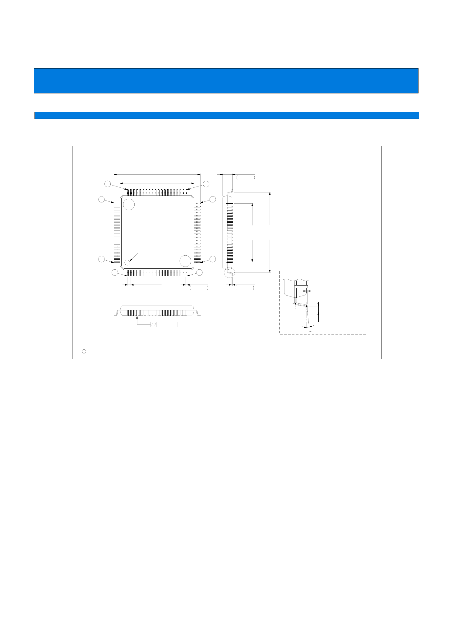
MB90242A Series
■ PACKAGE DIMENSIONS
80-pin Plastic LQFP
(FPT-80P-M05)
14.00±0.20(.551±.008)SQ
60
61 40
80
12.00±0.10(.472±.004)SQ
INDEX
To Top / Lineup / Index
+0.20
−0.10
1.50
(Mounting height)
+.008
.059
41
21
−.004
9.50
(.374)
REF
13.00
(.512)
NOM
LEAD No.
1
0.50±0.08
(.0197±.0031)
0.10(.004)
C
1995 FUJITSU LIMITED F80008S-2C-5
0.18
.007
20
+0.08
−0.03
+.003
−.001
"A"
0.127
.005
+0.05
−0.02
+.002
−.001
Details of "A" part
0.10±0.10
(.004±.004)
(STAND OFF)
0.50±0.20(.020±.008)
0 10˚
Dimensions in mm (inches)
56

FUJITSU LIMITED
For further information please contact:
Japan
FUJITSU LIMITED
Corporate Global Business Support Division
Electronic Devices
KAWASAKI PLANT, 4-1-1, Kamikodanaka
Nakahara-ku, Kawasaki-shi
Kanagawa 211-88, Japan
Tel: (044) 754-3763
Fax: (044) 754-3329
North and South America
FUJITSU MICROELECTRONICS, INC.
Semiconductor Division
3545 North First Street
San Jose, CA 95134-1804, U.S.A.
Tel: (408) 922-9000
Fax: (408) 432-9044/9045
Europe
FUJITSU MIKROELEKTRONIK GmbH
Am Siebenstein 6-10
63303 Dreieich-Buchschlag
Germany
Tel: (06103) 690-0
Fax: (06103) 690-122
Asia Pacific
FUJITSU MICROELECTRONICS ASIA PTE. LIMITED
#05-08, 151 Lorong Chuan
New Tech Park
Singapore 556741
Tel: (65) 281-0770
Fax: (65) 281-0220
To Top / Lineup / Index
MB90242A Series
All Rights Reserved.
The contents of this document are subject to change without
notice. Customers are advised to consult with FUJITSU sales
representatives before ordering.
The information and circuit diagrams in this document presented
as examples of semiconductor device applications, and are not
intended to be incorporated in devices for actual use. Also,
FUJITSU is unable to assume responsibility for infringement of
any patent rights or other rights of third parties arising from the
use of this information or circuit diagrams.
FUJITSU semiconductor devices are intended for use in
standard applications (computers, office automation and other
office equipment, industrial, communications, and measurement
equipment, personal or household devices, etc.).
CAUTION:
Customers considering the use of our products in special
applications where failure or abnormal operation may directly
affect human lives or cause physical injury or property damage,
or where extremely high levels of reliability are demanded (such
as aerospace systems, atomic energy controls, sea floor
repeaters, vehicle operating controls, medical devices for life
support, etc.) are requested to consult with FUJITSU sales
representatives before such use. The company will not be
responsible for damages arising from such use without prior
approval.
Any semiconductor devices have inherently a certain rate of
failure. You must protect against injury, damage or loss from
such failures by incorporating safety design measures into your
facility and equipment such as redundancy, fire protection, and
prevention of over-current levels and other abnormal operating
conditions.
F9704
FUJITSU LIMITED Printed in Japan
If any products described in this document represent goods or
technologies subject to certain restrictions on export under the
Foreign Exchange and Foreign Trade Control Law of Japan, the
prior authorization by Japanese government should be required
for export of those products from Japan.
57
 Loading...