


查询MB89635R供应商
FUJITSU SEMICONDUCTOR
DATA SHEET
DS07-12531-2E
8-bit Proprietary Microcontroller
CMOS
F2MC-8L MB89630R Series
MB89635R/T635R/636R/637R/T637R
MB89P637/W637/PV630
OUTLINE
■
The MB89630R series has been developed as a general-purpose version of the F2MC*-8L family consisting of
proprietary 8-bit, single-chip microcontrollers.
In addition to a compact instruction set, the microcontrollers contain a variety of peripheral functions such as
dual-clock control system, five operating speed control stages, a UART, timers, a PWM timer, a serial interface,
an A/D converter, an external interrupt, and a watch prescaler.
2
MC stands for FUJITSU Flexible Microcontroller.
*: F
FEATURES
■
• High-speed operating capability at low voltage
• Minimum execution time: 0.4 µs@3.5 V, 0.8 µs@2.7 V
2
•F
MC-8L family CPU core
Multiplication and division instructions
Instruction set optimized for controllers
• Five types of timers
8-bit PWM timer: 2 channels (Also usable as a reload timer)
8-bit pulse-width count timer (Continuous measurement capable, applicable to remote control, etc.)
16-bit timer/counter
21-bit timebase timer
•UART
CLK-synchronous/CLK-asynchronous data transfer capable (6, 7, and 8 bits)
• Serial interface
Switchable transfer direction to allows communication with various equipment.
• 10-bit A/D converter
Start by an external input capable
16-bit arithmetic operations
Test and branch instructions
Bit manipulation instructions, etc.
(Continued)
MB89630R Series
(Continued)
• External interrupt: 4 channels
Four channels are independent and capable of wake-up from low-power consumption modes (with an edge
detection function).
• Low-power consumption modes
Stop mode (Oscillation stops to minimize the current consumption.)
Sleep mode (The CPU stops to reduce the current consumption to approx. 1/3 of normal.)
Subclock mode
Watch mode
• Bus interface function
With hold and ready function
PACKAGE
■
64-pin Plastic SH-DIP
(DIP-64P-M01)
64-pin Ceramic SH-DIP
(DIP-64C-A06)
64-pin Plastic QFP
(FPT-64P-M06)
64-pin Ceramic MQFP
(MQP-64C-P01)
64-pin Plastic QFP
(FPT-64P-M09)
64-pin Ceramic MDIP
(MDP-64C-P02)
2
PRODUCT LINEUP
■
Part number
Item
MB89635R
MB89630R Series
MB89636R MB89637R MB89T635R MB89T637R MB89P637 MB89W637 MB89PV630
Classification
Mass-produced products
(mask ROM products)
ROM s ize
RAM size 512 × 8 bits 768 × 8 bits 1024 × 8 bits 512 × 8 bi t s 1024 × 8 bits 1 K
CPU functions The number of instructionns: 136
Ports Input ports: 5 (All also serve as peripherals.)
16 K × 8 bits
(internal
mask ROM)
Instruction bit length: 8 bits
Instruction length: 1 to 3 bytes
Data bit length: 1, 8, 16 bits
Minimum execution time: 0.4 to 6.4 µs/10 MHz, 61 µs@32.768 kHz
Interrupt processing time: 3.6 to 57.6 µs/10 MHz, 562.5 µs@32.768 kHz
Output ports (N-ch open-drain): 8 (All also serve as peripherals.)
I/O ports (N-ch open-drain): 4 (All also serve as peripherals.)
Output ports (CMOS): 8 (All also serve as bus control.)
I/O ports (CMOS): 28 (27 ports also serve as bus pins and peripherals.)
Total: 53
24 K × 8 bits
(internal
mask ROM)
32 K × 8 bits
(internal
mask ROM)
External ROM
products
Fixed to external ROM
One-time
PROM
product
32 K × 8 bits
(Internal PROM, to be
programmed with
general-purpose
EPROM programmer)
EPROM
product
Piggyback/
evaluation
product (for
evaluation
and
development)
32 K × 8 bits
(external
ROM)
× 8 bits
Clock timer 21 bits × 1 (in main clock)/15 bits × 1 (at 32.768 kHz)
8-bit PWM
timer
8-bit pulse
width count
timer
16-bit timer/
counter
8-bit serial I/O 8 bits
UART Capable of switching two I/O systems by software
10-bit A/D
converter
8-bit reload timer operation (toggled output capable, operating clock cycle: 0.4 µs to 3.3 ms) × 2
channels
7/8-bit resolution PWM operation (conversion cycle: 51.2 µs to 839 ms) × 2 channels
8-bit timer operation (overflow output capable, operating clock cycle: 0.4 to 12.8 µs)
8-bit reload timer operation (toggled output capable, operating clock cycle: 0.4 to 12.8 µs)
8-bit pulse width measurement operation (capable of continuous measurement, and
measurement of “H” pulse width/ “L” pulse width/ from ↑ to ↑/from ↓ to ↓)
16-bit timer operation (operating clock cycle: 0.4 µs)
16-bit event counter operation (rising edge/falling edge/both edge selectable)
LSB first/MSB first selectable
One clock selectable from four transfer clocks
(one external shift clock, three internal shift clocks: 0.8 µs, 3.2 µs, 12.8 µs)
Transfer data length (6, 7, and 8 bits)
Transfer rate (300 to 62500 bps. at 10 MHz osciliation)
10-bit resolution × 8 channels
A/D conversion mode (conversion time: 13.2 µs)
Sense mode (conversion time: 7.2 µs)
Capable of continuous activation by an external activation or an internal timer
(Continued)
3
MB89630R Series
(Continued)
Part number
Item
MB89635R
MB89636R MB89637R MB89T635R MB89T637R MB89P637 MB89W637 MB89PV630
External
interrupt input
Used also for wake-up from stop/sleep mode. (Edge detection is also permitted in stop mode.)
Standby mode Sleep mode, stop mode, watch mode, and subclock mode
Process CMOS
Operating
voltage*
EPROM for use
* :Varies with conditions such as the operating frequency. (See section “■ Electrical Characteristics.”)
In the case of the MB89PV630, the voltage varies with the restrictions of the EPROM for use.
PACKAGE AND CORRESPONDING PRODUCTS
■
Package
DIP-64P-M01 ××
FPT-64P-M06 ××
FPT-64P-M09 ×* ×* ×*
DIP-64C-A06 ××× ×
MB89635R
MB89T635R
4 independent channels (edge selection, interrupt vector, source flag).
Rising edge/falling edge selectable
2.2 V to 6.0 V 2.7 V to 6.0 V
MB89636R
MB89637R
MB89T637R
MB89P637 MB89W637 MB89PV630
MBM27C256A-20CZ
MBM27C256A-20TV
MQP-64C-P01 ××××
MDP-64C-P02 ××××
: Available ×: Not available
* :To convert pin pitches, an adapter socket (manufacturer: Sun Hayato Co., Ltd.) is available.
64SD-64QF2-8L: For conversion from (DIP-64P-M01, DIP-64C-A06, or MDP-64C-P02) to FPT-64P-M09
Inquiry: Sun Hayato Co., Ltd.: TEL (81)-3-3986-0403
FAX (81)-3-5396-9106
Note: For more information about each package, see section “■ Package Dimensions.”
4
MB89630R Series
DIFFERENCES AMONG PRODUCTS
■
1. Memory Size
Before e valuating using the piggyback product, verify its differences from the product that will actually be used.
Take particular care on the following points:
On the MB89P637/W637, the program area starts from address 8007
starts from 8000
• On the MB89P637/W637, addresses 8000
H.
H to 8006H comprise the option setting area, option settings can be
read by reading these addresses. On the MB89PV630/MB89637R, addresses 8000
H but on the MB89PV630 and MB89637R
H to 8006H could also be
used as a program ROM. However, do not use these addresses in order to maintain compatibility of the
MB89P637/W637.
• The stack area, etc., is set at the upper limit of the RAM.
• The external area is used.
2. Current Consumption
• In the case of the MB89PV630, add the current consumed by the EPROM which connected to the top socket.
• When operated at low speed, the product with an OTPROM (one-time PROM) or an EPROM will consume
more current than the product with a mask ROM. However, the current consumption in sleep/stop modes is
the same. (For more inf ormation, see sections “■ Electrical Characteristics” and “■ Example Characteristics.”)
3. Mask Options
Functions that can be selected as options and how to designate these options vary by the product.
Before using options check section “■ Mask Options.”
Take particular care on the following points:
• A pull-up resistor cannot be set for P50 to P53 on the MB89P637 and MB89W637.
• Options are fixed on the MB89PV630, MB89T635R, and MB89T637R.
4. Differences between the MB89630 and MB89630R Series
• Memory access area
There are no difference between the access area of MB89635/MB89635R, and that of MB89637/MB89637R.
The access area of MB89636 is different from that of the MB89636R when using in external bus mode.
Address
MB89636 MB89636R
H to 007FH I/O area I/O area
0000
0080
H to 037FH RAM area RAM area
0380
H to 047FH
0480H to 7FFFH External area
External area
8000H to 9FFFH Access prohibited
A000
H to FFFFH ROM area ROM area
Memory area
Access prohibited
5

MB89630R Series
• Other specifications
Both MB89630 series and MB89630R is the same.
• Electrical specifications/electrical characteristics
Electrical specifications of the MB89630R series are the same as that of the MB89630 series.
Electrical characteristics of both the series are much the same.
CORRESPONDENCE BETWEEN THE MB89630 AND MB89630R SERIES
■
• The MB89630R series is the reduction version of the MB89630 series.
• The the MB89630 and MB89630R series consist of the following products:
MB89630 series MB89635 MB89T635 MB89636 MB89637 MB89T637
MB89630R series MB89635R MB89T635R MB89636R MB89637R MB89T637R
MB89P637 MB89W637 MB89PV630
6

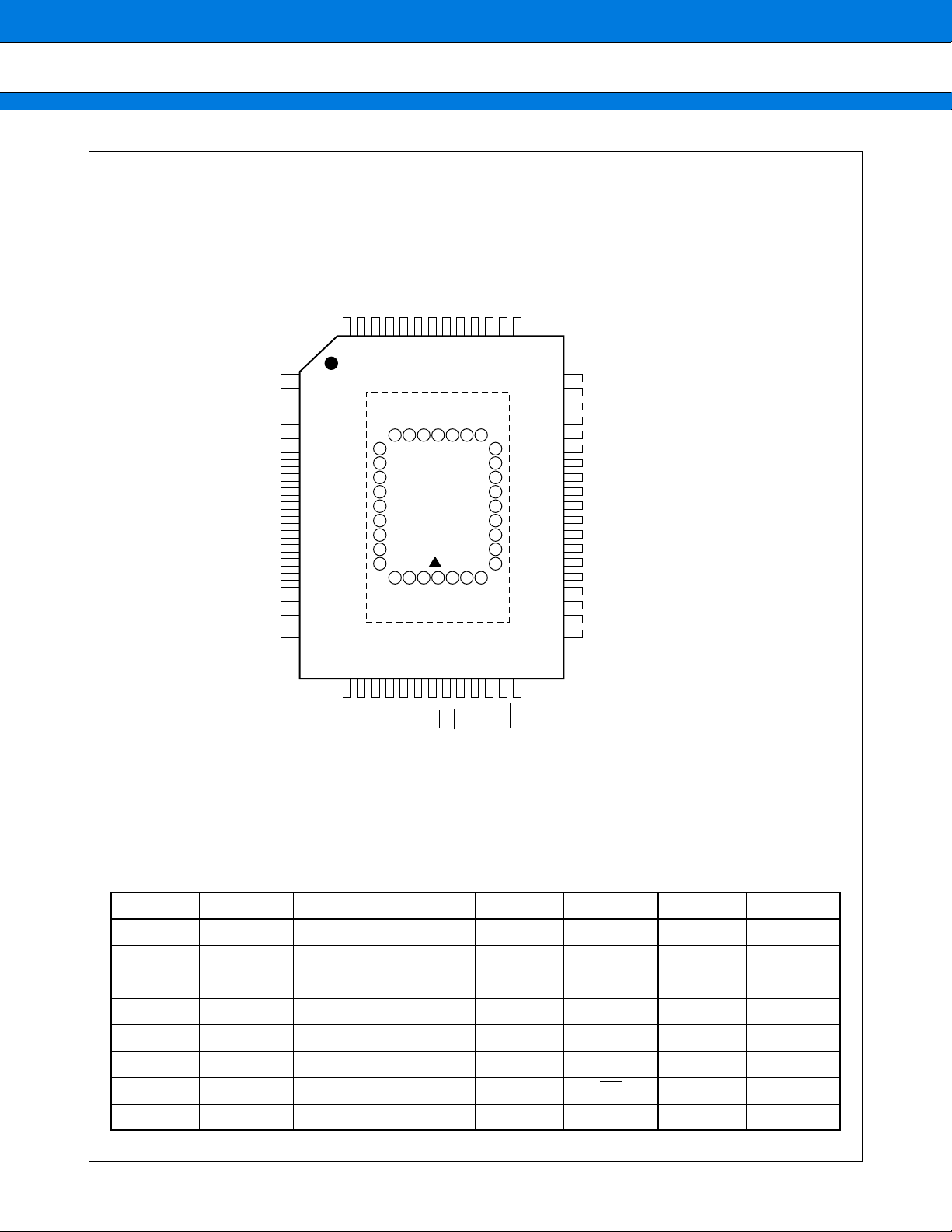
PIN ASSIGNMENT
■
MB89630R Series
(Top view)
P31/UO1
P30/UCK1
P43/PTO1
P42/UI2
P41/UO2
P40/UCK2
P53/PTO2
P52
P51/BZ
P50/ADST
P60/AN0
P61/AN1
P62/AN2
P63/AN3
P64/AN4
P65/AN5
P66/AN6
P67/AN7
CC
AV
AVR
SS
AV
P74/EC
P73/INT3
P72/INT2
P71/INT1/X0A*
P70/INT0/X1A*
RST
MOD0
MOD1
X0
X1
V
SS
1
2
3
4
5
6
7
8
9
10
11
12
13
14
15
16
17
18
19
20
21
22
23
24
25
26
27
28
29
30
31
32
65
PP
V
66
A12
67
A7
68
A6
69
A5
70
A4
71
A3
72
A2
73
A1
74
A0
75
O1
76
O2
77
O3
78
VSS
(DIP-64P-M01)
(DIP-64C-A06)
(MDP-64C-P02)
VCC
92
A14
91
A13
90
A8
89
A9
88
A11
87
86
OE
A10
85
84
CE
O8
83
O7
82
O6
81
O5
80
O4
79
Each pin inside
the dashed line is
for MB89PV630 only.
(Top view)
VCC
64
P32/UI1
63
P33/SCK1
62
P34/SO1
61
P35/SI1
60
P36/PWC
59
P37/WTO
58
V
57
56
55
54
53
52
51
50
49
48
47
46
45
44
43
42
41
40
39
38
37
36
35
34
33
SS
P00/AD0
P01/AD1
P02/AD2
P03/AD3
P04/AD4
P05/AD5
P06/AD6
P07/AD7
P10/A08
P11/A09
P12/A10
P13/A11
P14/A12
P15/A13
P16/A14
P17/A15
P20/BUFC
P21/HAK
P22/HRQ
P23/RDY
P24/CLK
P25/WR
P26/RD
P27/ALE
*: When the dual-clock system is selected.
P51/BZ
P50/ADST
P60/AN0
P61/AN1
P62/AN2
P63/AN3
P64/AN4
P65/AN5
P66/AN6
P67/AN7
AV
CC
AVR
AV
SS
P74/EC
P73/INT3
P72/INT2
P52
P53/PTO2
P40/UCK2
P41/UO2
P42/UI2
P43/PTO1
P30/UCK1
P31/UO1
646362616059585756555453525150
1
2
3
4
5
6
7
8
9
10
11
12
13
14
15
16
171819202122232425262728293031
P71/INT1/X0A*
P70/INT0/X1A*
RST
MOD0
SS
MOD1X0X1
V
(FPT-64P-M09) *: When the dual-clock system is selected.
CC
P32/UI1
P33/SCK1
V
P27/ALE
P26/RD
P25/WR
P34/SO1
P35/SI1
P36/PWC
P24/CLK
P23/RDY
P22/HRQ
SS
P37/WTO
V
49
48
47
46
45
44
43
42
41
40
39
38
37
36
35
34
33
32
P21/HAK
P20/BUFC
P00/AD0
P01/AD1
P02/AD2
P03/AD3
P04/AD4
P05/AD5
P06/AD6
P07/AD7
P10/A08
P11/A09
P12/A10
P13/A11
P14/A12
P15/A13
P16/A14
P17/A15
7
MB89630R Series
(Top view)
CC
P32/UI1
P33/SCK1
P34/SO1
P53/PTO2
P40/UCK2
P41/UO2
P42/UI2
P43/PTO1
P30/UCK1
P31/UO1
V
64636261605958575655545352
P35/SI1
P36/PWC
P52
P51/BZ
P50/ADST
P60/AN0
P61/AN1
P62/AN2
P63/AN3
P64/AN4
P65/AN5
P66/AN6
P67/AN7
AV
CC
AVR
AV
SS
P74/EC
P73/INT3
P72/INT2
P71/INT1/X0A*
P70/INT0/X1A*
1
2
3
4
5
6
7
8
9
10
11
12
13
14
15
16
17
18
19
Each pin inside the dashed line
is for MB89PV630 only.
20212223242526272829303132
RST
84838281807978
85
86
87
88
89
90
91
92
93
94959665666768
MOD0
SS
MOD1X0X1
V
(FPT-64P-M06)
(MQP-64C-P01)
P27/ALE
77
76
75
74
73
72
71
70
69
P26/RD
P25/WR
P24/CLK
P23/RDY
P22/HRQ
P21/HAK
51
P37/WTO
50
49
48
47
46
45
44
43
42
41
40
39
38
37
36
35
34
33
*: When the dual-clock system is selected.
SS
V
P00/AD0
P01/AD1
P02/AD2
P03/AD3
P04/AD4
P05/AD5
P06/AD6
P07/AD7
P10/A08
P11/A09
P12/A10
P13/A11
P14/A12
P15/A13
P16/A14
P17/A15
P20/BUFC
• Pin assignment on package top (MB89PV630 only)
Pin no. Pin name Pin no. Pin name Pin no. Pin name Pin no. Pin name
65 N.C. 73 A2 81 N.C. 89 OE
66 VPP 74 A1 82 O4 90 N.C.
67A1275A083O591A11
68 A7 76 N.C. 84 O6 92 A9
69 A6 77 O1 85 O7 93 A8
70 A5 78 O2 86 O8 94 A13
71 A4 79 O3 87 CE
72 A3 80 V
N.C.: Internally connected. Do not use.
8
95 A14
SS 88 A10 96 VCC

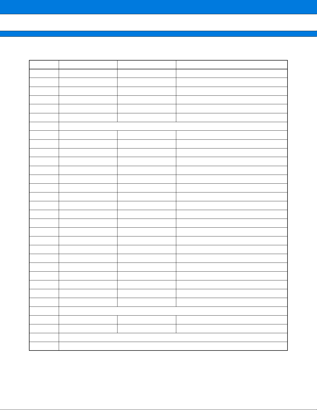
PIN DESCRIPTION
■
MB89630R Series
Pin no.
SH-DIP
*2
MDIP
*1
QFP2
*3
QFP1
MQFP
*4
*5
Pin name
Circuit
type
Function
30 22 23 X0 A Main clock crystal oscillator pins
31 23 24 X1
28 20 21 MOD0 D Operating mode selection pins
29 21 22 MOD1
Connect directly to V
CC or VSS.
27 19 20 RST C Reset I/O pin
This pin is an N-ch open-drain output type with a
pull-up resistor, and a hysteresis input type.
“L” is output from this pin by an internal reset
source. The internal circuit is initialized by the
input of “L”.
56 to 49 48 to 41 49 to 42 P00/AD0 to
P07/AD7
F General-purpose I/O ports
When an external bus is used, these ports
function as the multiplex pins of the lo w er address
output and the data I/O.
48 to 41 40 to 33 41 to 34 P10/A08 to
P17/A157
F General-purpose I/O ports
When an external bus is used, these ports
function as an upper address output.
40 32 33 P20/BUFC H General-purpose output port
When an external bus is used, this port can also
be used as a buffer control output by setting the
BCTR.
39 31 32 P21/HAK
H General-purpose output port
When an external bus is used, this port can also
be used as a hold acknowledge by setting the
BCTR.
38 30 31 P22/HRQ F General-purpose output port
When an external bus is used, this port can also
be used as a hold request input by setting the
BCTR.
37 29 30 P23/RDY F General-purpose output port
When an external bus is used, this port functions
as a ready input.
36 28 29 P24/CLK H General-purpose output port
When an external bus is used, this port functions
as a clock output.
35 27 28 P25/WR
H General-purpose output port
When an external bus is used, this port functions
as a write signal output.
34 26 27 P26/RD
H General-purpose output port
When an external bus is used, this port functions
as a read signal output.
*1: DIP-64P-M01, DIP-64C-A06 *4: FPT-64P-M06
*2: MDP-64C-P02 *5: MQP-M64C-P01
*3: FPT-64P-M09
(Continued)
9

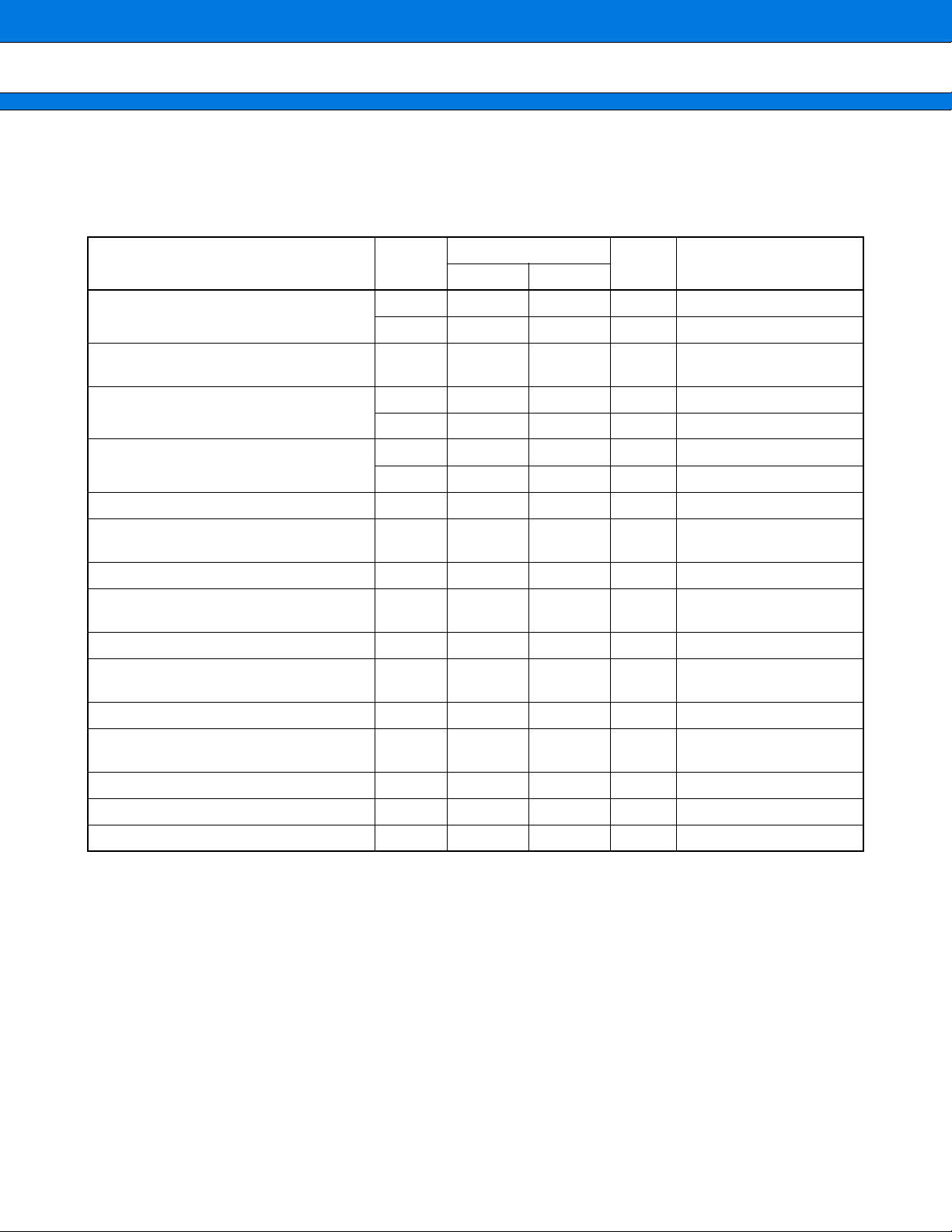
MB89630R Series
(Continued)
Pin no.
SH-DIP
*2
MDIP
*1
QFP2
*3
QFP1
MQFP
*4
*5
Pin name
33 25 26 P27/ALE H General-purpose output port
2 58 59 P30/UCK1 G General-purpose I/O port
1 57 58 P31/UO1 F General-purpose I/O port
63 55 56 P32/UI1 G General-purpose I/O port
62 54 55 P33/SCK1 G General-purpose I/O port
61 53 54 P34/SO1 F General-purpose I/O port
60 52 53 P35/SI1 G General-purpose I/O port
59 51 52 P36/PWC G General-purpose I/O port
58 50 51 P37/WTO F General-purpose I/O port
6 62 63 P40/UCK2 G General-purpose I/O port
5 61 62 P41/UO2 F General-purpose I/O port
4 60 61 P42/UI2 G General-purpose I/O port
3 59 60 P43/PTO1 F General-purpose I/O port
10 2 3 P50/ADST K General-purpose I/O port
Circuit
type
When an external bus is used, this port functions
as an address latch signal output.
Also serves as the clock I/O 1 for the UART.
This port is a hysteresis input type.
Also serves as the data output 1 for the UART.
Also serves as the data input 1 for the UART.
This port is a hysteresis input type.
Also serves as the data input for the 8-bit serial
I/O.
This port is a hysteresis input type.
Also serves as the data output for the 8-bit serial
I/O.
Also serves as the data input for the 8-bit serial
I/O.
This port is a hysteresis input type.
Also serves as the measured pulse input for the
8-bit pulse width counter.
This port is a hysteresis input type.
Also serves as the toggle output for the 8-bit pulse
width counter.
Also serves as the clock I/O 2 for the UART.
This port is a hysteresis input type.
Also serves as the data output 2 for the UART.
Also serves as the data input 2 for the UART.
This port is a hysteresis input type.
Also serves as the toggle output for the 8-bit PWM
timer.
Also serves as an A/D converter external
activation.
This port is a hysteresis input type.
Function
*1: DIP-64P-M01, DIP-64C-A06 *4: FPT-64P-M06
*2: MDP-64C-P02 *5: MQP-M64C-P01
*3: FPT-64P-M09
10
(Continued)
(Continued)
MB89630R Series
Pin no.
SH-DIP
*2
MDIP
*1
QFP2
*3
QFP1
MQFP
*4
*5
Pin name
Circuit
type
9 1 2 P51/BZ J General-purpose I/O port
Also serves as a buzzer output.
8 64 1 P52 J General-purpose I/O port
7 63 64 P53/PTO2 J General-purpose I/O port
Also serves as the toggle output for the 8-bit PWM
timer.
11 to 18 3 to 10 4 to 11 P60/AN0 to
P67/AN7
26,
25
18,
17
19,18P70/INT0/X1A,
P71/INT1/X0A
I N-ch open-drain output ports
Also serve as an A/D converter analog input.
B/E Input-only ports
These ports are a hysteresis input type.
Also serve as an external interrupt input (at single-
clock operation).
Subclock crystal oscillator pins (at dual-clock
operation)
24,
23
16,
15
17,16P72/INT2,
P73/INT3
E Input-only ports
Also serve as an external interrupt input.
These ports are a hysteresis input type.
22 14 15 P74/EC E General-purpose input port
Also serves as the external clock input for the
16-bit timer/counter.
This port is a hysteresis input type.
Function
64 56 57 V
32, 57 24,49 25, 50 V
CC — Power supply pin
SS — Power supply (GND) pin
19 11 12 AVCC — A/D converter power supply pin
20 12 13 AVR — A/D converter reference voltage input pin
21 13 14 AV
SS — A/D converter power supply pin
Use this pin at the same voltage as V
*1: DIP-64P-M01, DIP-64C-A06 *4: FPT-64P-M06
*2: MDP-64C-P02 *5: MQP-M64C-P01
*3: FPT-64P-M09
SS.
11
MB89630R Series
•
External EPROM pins (MB89PV630 only)
Pin no.
MDIP MQFP
65 66 V
66
67
68
69
70
71
72
73
74
75
76
77
67
68
69
70
71
72
73
74
75
77
78
79
78 80 V
79
80
81
82
83
82
83
84
85
86
84 87 CE
Pin name I/O Function
PP O “H” level output pin
A12
O Address output pins
A7
A6
A5
A4
A3
A2
A1
A0
O1
I Data input pins
O2
O3
SS O Power supply (GND) pin
O4
I Data input pins
O5
O6
O7
O8
O ROM chip enable pin
Outputs “H” during standby.
85 88 A10 O Address output pin
86 89 OE
O ROM output enable pin
Outputs “L” at all times.
87
88
89
91
92
93
A11
A9
A8
O Address output pins
90 94 A13 O
91 95 A14 O
92 96 V
—65
76
CC O EPROM power supply pin
N.C. — Internally connected pins
Be sure to leave them open.
81
90
12
MB89630R Series
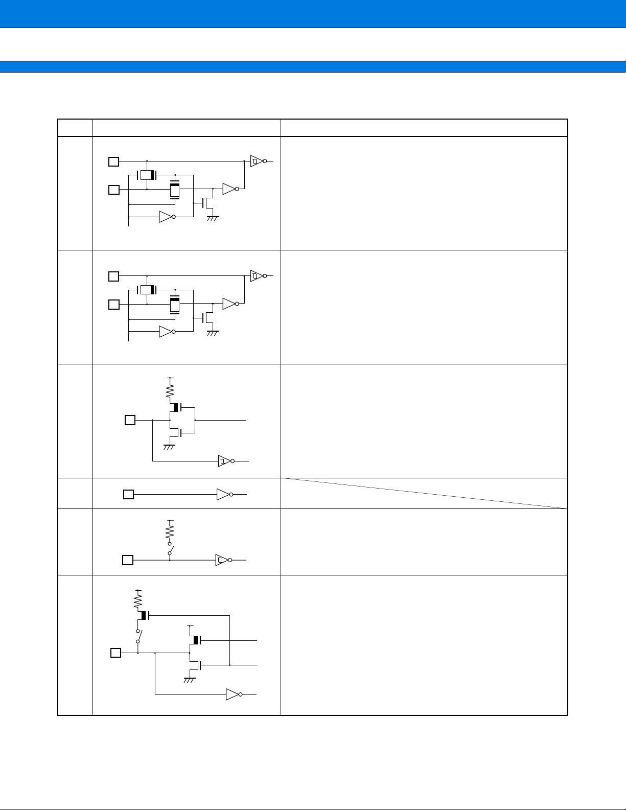
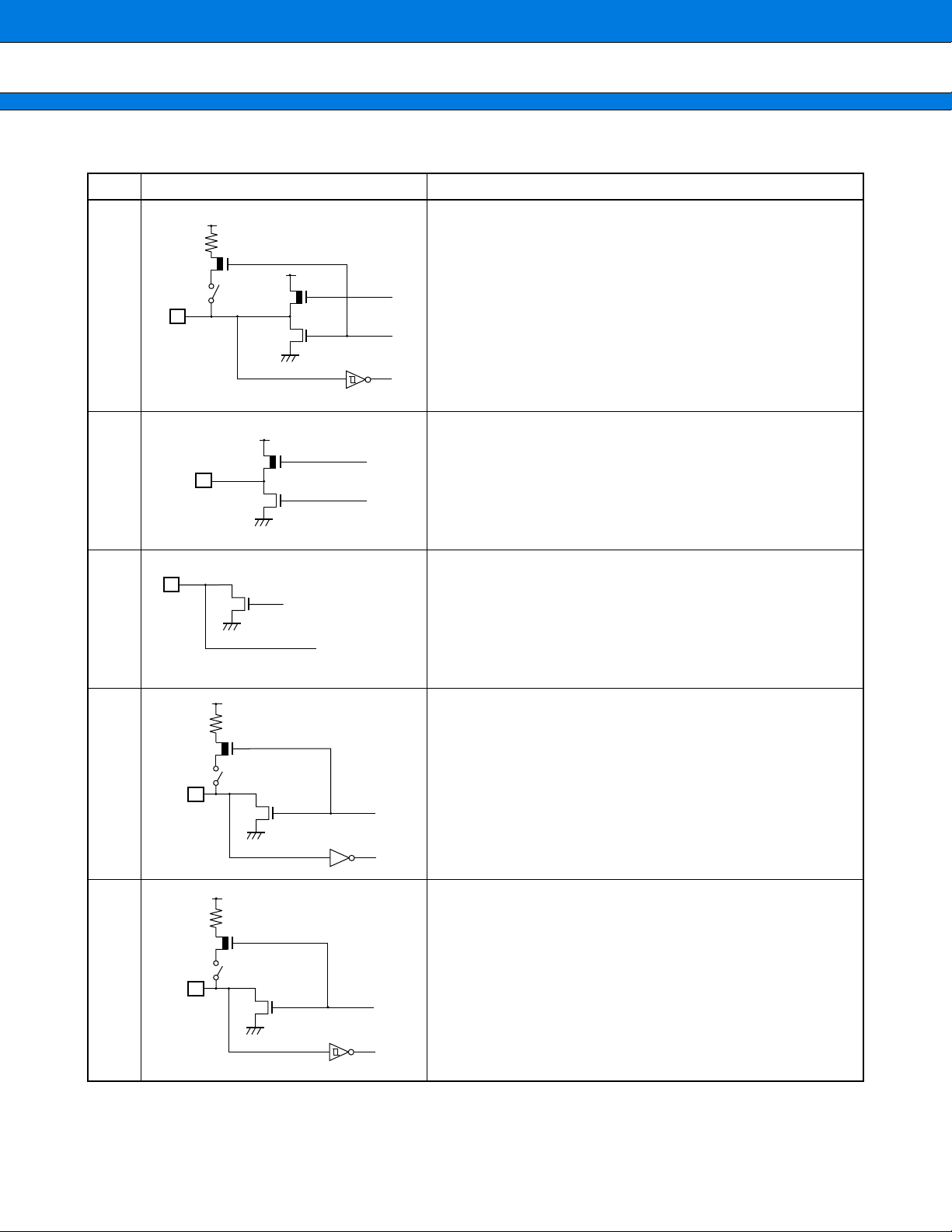
I/O CIRCUIT TYPE
■
Type Circuit Remarks
A • Crystal or ceramic oscillation type (main clock)
X1
External clock input selection versions of MB89PV630,
MB89P637, MB89W637, MB89635R, MB89T635R,
X0
MB89636R, MB89637R, and MB89T637R
At an oscillation feedback resistor of approximately
1 MΩ@5.0 V
Standby control signal
B • Crystal or ceramic oscillation type (subclock)
X1A
MB89PV630, MB89P637, MB89W637, MB89635R,
MB89636R, and MB89637R with dual-clock system
X0A
At an oscillation feedback resistor of approximately
4.5 MΩ@5.0 V
Standby control signal
C •At an output pull-up resistor (P-ch) of approximately
R
P-ch
N-ch
50 kΩ@5.0 V
• Hysteresis input
D
E • Hysteresis input
R
• Pull-up resistor optional (except P70 and P71)
F • CMOS output
R
P-ch
P-ch
N-ch
•CMOS input
• Pull-up resistor optional (except P22 and P23)
(Continued)
13
MB89630R Series
(Continued)
Type Circuit Remarks
G •CMOS output
• Hysteresis input
R
P-ch
P-ch
N-ch
• Pull-up resistor optional
H •CMOS output
P-ch
N-ch
I • Analog input
N-ch
Analog input
J•CMOS input
R
P-ch
N-ch
• Pull-up resistor optional
K • Hysteresis input
R
P-ch
N-ch
• Pull-up resistor optional
14

MB89630R Series
HANDLING DEVICES
■
1. Preventing Latchup
Latchup may occur on CMOS ICs if voltage higher than VCC or lower than VSS is applied to input and output pins
other than medium- and high-voltage pins or if higher than the voltage which shows on “1. Absolute Maximum
Ratings” in section “■ Electrical Characteristics” is applied between V
When latchup occurs, power supply current increases rapidly and might thermally damage elements. When
using, take great care not to exceed the absolute maximum ratings.
CC and VSS.
Also, tak e care to prev ent the analog po wer supply (AV
power supply (VCC) when the analog system power supply is turned on and off.
CC and A VR) and analog input from e xceeding the digital
2. Treatment of Unused Input Pins
Leaving unused input pins open could cause malfunctions. The y should be connected to a pull-up or pull-down
resistor.
3. Treatment of Power Supply Pins on Microcontrollers with A/D and D/A Converters
Connect to be AVCC = DAVC = VCC and AVSS = AVR = VSS even if the A/D and D/A converters are not in use.
4. Treatment of N.C. Pins
Be sure to leave (internally connected) N.C. pins open.
5. Power Supply Voltage Fluctuations
Although VCC power supply voltage is assured to oper ate within the rated range, a rapid fluctuation of the v oltage
could cause malfunctions, ev en if it occurs within the rated range. Stabilizing voltage supplied to the IC is therefore
important. As stabilization guidelines, it is recommended to control power so that V
value) will be less than 10% of the standard VCC value at the commercial frequency (50 Hz to 60 Hz) and the
transient fluctuation rate will be less than 0.1 V/ms at the time of a momentary fluctuation such as when power
is switched.
CC ripple fluctuations (P-P
6. Precautions when Using an External Clock
When an external clock is used, oscillation stabilization time is required ev en for power-on reset (option selection)
and wake-up from stop mode.
15
MB89630R Series
PROGRAMMING TO THE EPROM ON THE MB89P637
■
The MB89P637 is an OTPROM version of the MB89630 series.
1. Features
• 32-Kbytes PROM on chip
• Options can be set using the EPROM programmer.
• Equivalency to the MBM27C256A in EPROM mode (when programmed with the EPROM programmer)
2. Memory Space
Memory space in each mode is illustrated below.
0000H
0080H
0100H
0200H
0480H
8000H
8007H
Normal operating mode
I/O
Register RAM
External area
Option setting area
PROM
32 KB
EPROM mode
(Corresponding addresses
on the EPROM programmer)
H
0000
0007H
Option setting area
Program area
(EPROM)
32 KB
7FFF
FFFFH
H
3. Programming to the EPPROM
In EPROM mode, the MB89P637 functions equivalent to the MBM27C256A. This allows the PROM to be
programmed with a general-purpose EPROM programmer by using the dedicated socket adapter.
However, the electronic signature mode cannot be used.
When the operating ROM area for a single chip is 32 Kbytes (8007
as follows:
16
H to FFFFH) the EPROM can be programmed

MB89630R Series
•
Programming procedure
(1) Set the EPROM programmer to the MBM27C256A-20CZ and MBM27C256A-20TV.
(2) Load program data into the EPROM programmer at 0007
in the operating mode assign to 0000H to 7FFFH in EPROM mode).
H to 7FFFH. (Note that addresses 8000H to FFFFH
(3) Load option data into addresses 0000
H to 0006H of the EPROM programmer.
(For information about each corresponding option, see “8. OTPROM Option Bit Map.”)
(4) Program with the EPROM programmer.
4. Recommended Screening Conditions
High-temperature aging is recommended as the pre-assembly screening procedure for a product with a blanked
OTPROM microcomputer program.
Program, verify
Aging
+150°C, 48 Hrs.
Data verification
Assembly
5. Programming Yield
All bits cannot be programmed at Fujitsu shipping test to a blank ed O TPROM microcomputer, due to its nature.
For this reason, a programming yield of 100% cannot be assured at all times.
6. Erasure
In order to clear all locations of their programmed contents, it is necessary to expose the internal EPROM to an
ultraviolet light source. A dosage of 10 W -seconds/cm
dosage can be obtained by exposure to an ultraviolet lamp (wavelength of 2537 Angstroms (Å)) with intensity
of 12000 µW/cm
2
for 15 to 21 minutes. The internal EPROM should be about one inch from the source and all
filters should be removed from the UV light source prior to erasure.
It is important to note that the internal EPROM and similar devices, will erase with light sources having wave-
lengths shorter than 4000 Å. Although erasure time will be much longer than with UV source at 2537 Å,
nevertheless the exposure to fluorescent light and sunlight will eventually erase the internal EPROM, and
exposure to them should be prevented to realize maximum system reliability. If used in such an environment,
the package windows should be covered by an opaque label or substance.
2
is required to completely erase an internal EPROM. This
17

MB89630R Series
7. EPROM Programmer Socket Adapter
Part No.
Package
Compatible socket adapter
Sun Hayato Co., Ltd.
Inquiry: Sun Hayato Co., Ltd.: TEL : (81)-3-3986-0403
FAX: (81)-3-5396-9106
8. OTPROM Option Bit Map
Address
0000
H
0001H
H
0002
H
0003
H
0004
H
0005
0006H
Bit 7 Bit 6 Bit 5 Bit 4 Bit 3 Bit 2 Bit 1 Bit 0
Vacancy
Readable
and writable
P07
Pull-up
1: No
0: Yes
P17
Pull-up
1: No
0: Yes
P37
Pull-up
1: No
0: Yes
Vacancy
Readable
and writable
Vacancy
Readable
and writable
Vacancy
Readable
and writable
Vacancy
Readable
and writable
P06
Pull-up
1: No
0: Yes
P16
Pull-up
1: No
0: Yes
P36
Pull-up
1: No
0: Yes
Vacancy
Readable
and writable
Vacancy
Readable
and writable
Vacancy
Readable
and writable
Vacancy
Readable
and writable
P05
Pull-up
1: No
0: Yes
P15
Pull-up
1: No
0: Yes
P35
Pull-up
1: No
0: Yes
Vacancy
Readable
and writable
Vacancy
Readable
and writable
Vacancy
Readable
and writable
MB89P637-SH MB89P637PF
SH-DIP-64 QFP-64
ROM-64SD-28DP-8L ROM-64QF-28DP-8L
Single/dualclock system
1: Dual clock
0: Single clock
P04
Pull-up
1: No
0: Yes
P14
Pull-up
1: No
0: Yes
P34
Pull-up
1: No
0: Yes
Vacancy
Readable
and writable
P74
Pull-up
1: No
0: Yes
Vacancy
Readable
and writable
Reset pin
output
1: Yes
0: No
P03
Pull-up
1: No
0: Yes
P13
Pull-up
1: No
0: Yes
P33
Pull-up
1: No
0: Yes
P43
Pull-up
1: No
0: Yes
P73
Pull-up
1: No
0: Yes
Vacancy
Readable
and writable
Power-on
reset
1: Yes
0: No
P02
Pull-up
1: No
0: Yes
P12
Pull-up
1: No
0: Yes
P32
Pull-up
1: No
0: Yes
P42
Pull-up
1: No
0: Yes
P72
Pull-up
1: No
0: Yes
Vacancy
Readable
and writable
Oscillation stabilization (/FCH)
11:218/FCH 01:217/FCH
10:214/FCH 00:24/FCH
P01
Pull-up
1: No
0: Yes
P11
Pull-up
1: No
0: Yes
P31
Pull-up
1: No
0: Yes
P41
Pull-up
1: No
0: Yes
Vacancy
Readable
and writable
Vacancy
Readable
and writable
P00
Pull-up
1: No
0: Yes
P10
Pull-up
1: No
0: Yes
P30
Pull-up
1: No
0: Yes
P40
Pull-up
1: No
0: Yes
Vacancy
Readable
and writable
Reserved bit
Readable
and writable
Note: Each bit is set to ‘1’ as the initialized value.
18

MB89630R Series
PROGRAMMING TO THE EPROM WITH PIGGYBACK/EVALUATION DEVICE
■
1. EPROM for Use
MBM27C256A-20CZ, MBM27C256A-20TV
2. Programming Socket Adapter
To program to the PROM using an EPROM programmer, use the socket adapter (manufacturer: Sun Hayato
Co., Ltd.) listed below.
Package Adapter socket part number
LCC-32 (Rectangle) ROM-32LC-28DP-YG
Inquiry: Sun Hayato Co., Ltd.: TEL: (81)-3-3986-0403
FAX: (81)-3-5396-9106
3. Memory Space
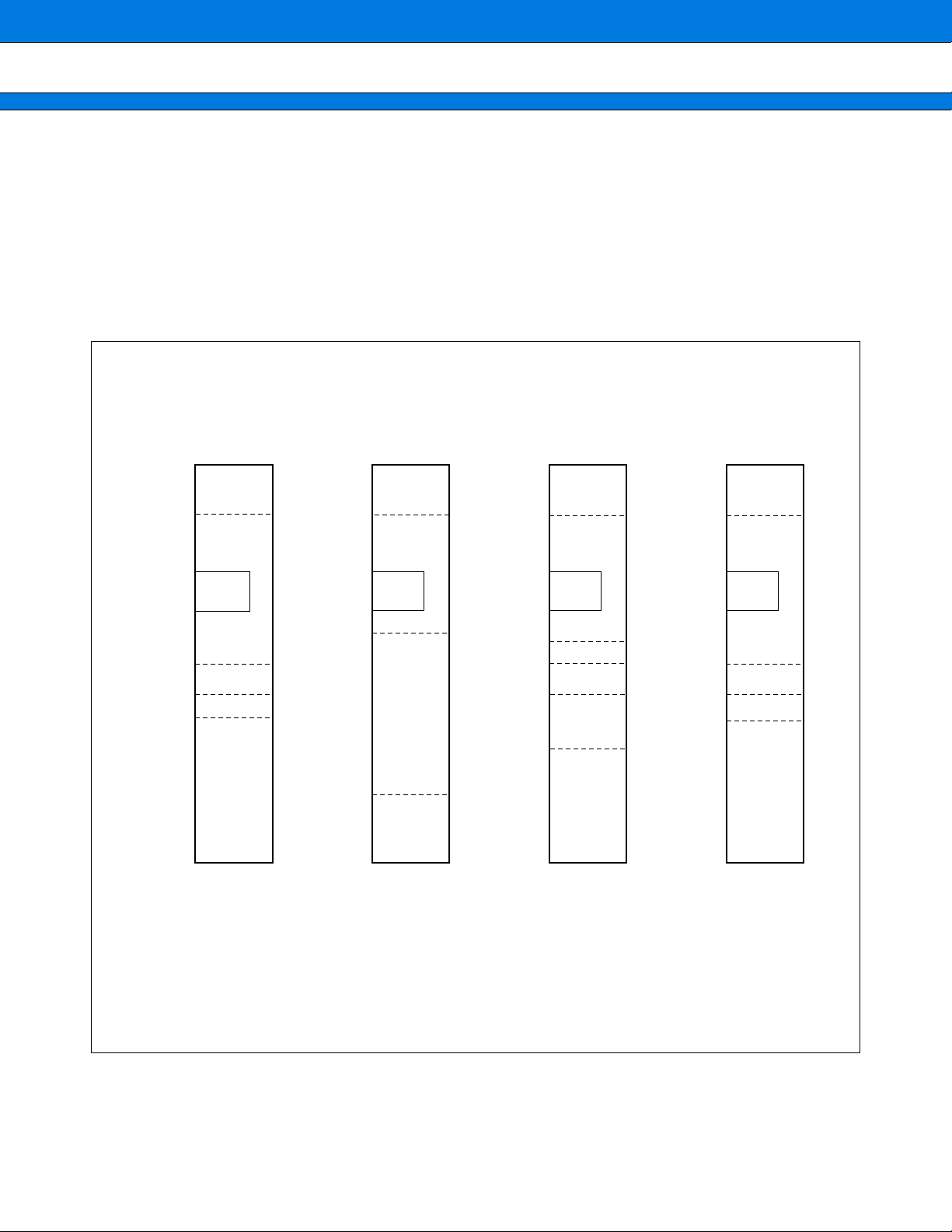
Memory space in each mode, such as 32-Kbyte PROM, option area is diagrammed below.
Address
0000H
0080H
0480H
8000H
8007H
FFFF
H
Single chip
I/O
RAM
Not available
Not available
PROM
32 KB
Corresponding addresses on the EPROM programmer
0000H
0007H
7FFF
H
4. Programming to the EPROM
(1) Set the EPROM programmer to the MBM27C256A.
(2) Load program data into the EPROM programmer at 0007H to 7FFFH.
Not available
EPROM
32 KB
(3) Program to 0000
H to 7FFFH with the EPROM programmer.
19
MB89630R Series
BLOCK DIAGRAM
■
X0
X1
X0A
X1A
RST
P00/AD0
to P07/AD7
P10/A08
to P17/A15
MOD0
MOD1
P27/ALE
P26/RD
P25/WR
P24/CLK
P23/RDY
P22/HRQ
P21/HAK
P20/BUFC
Main clock oscillator
Subclock oscillator
(32.768 kHz)
Clock controller
Reset circuit
(Watchdog timer)
Watch prescaler
8
8
CMOS I/O port
Port0 and port1Port 2
External bus
interface
CMOS output port
RAM
2
F MC-8L
CPU
Internal data bus
21-bit timebase timer
CMOS I/O port
8-bit PWC timer
8-bit serial I/O
UART
UART baud rate
generator
CMOS I/O port
N-ch open-drain I/O port
8-bit PWM timer
Buzzer output
10-bit A/D converter
Port 3Port 4
Port 5Port 6Port 7
3
8 8
P37/WTO
P36/PWC
P35/SI1
P34/SO1
P33/SCK1
P32/UI1
P31/UO1
P30/UCK1
P40/UCK2
P41/UO2
P42/UI2
P43/PTO1
P53/PTO2
P52
P51/BZ
P50/ADST
AVCC, AVSS,
AVR
P60/AN0
to P67/AN7
20
Other pins
VCC × 2, VSS × 2
ROM
N-ch open-drain output port
Input port
External interrupt
16-bit timer/counter
4
P70/INT0
P71/INT1
P72/INT2
P73/INT3
P74/EC
MB89630R Series
CPU CORE
■
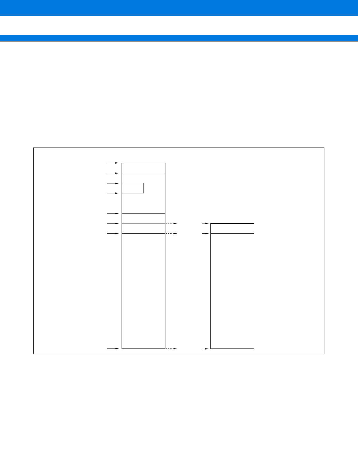
1. Memory Space
The microcontrollers of the MB89630R series offer 64 Kbytes of memory for storing all of I/O, data, and program
areas. The I/O area is located at the lowest address. The data area is provided immediately above the I/O area.
The data area can be divided into register, stack, and direct areas according to the application. The program
area is located at exactly the opposite end of I/O area, that is, near the highest address. Provide the tables of
interrupt reset vectors and vector call instructions toward the highest address within the program area. The
memory space of the MB89630R series is structured as illustrated below.
• Memory space
MB89637R
MB89T637R
0000H
MB89PV630
0000
MB89635R
MB89T635R
H
0000
MB89636R
H
0000
MB89P637
MB89W637
H
I/O
RAM
512 B
Register
External area
1
ROM*
16 KB
0080H
0100H
0200H
0380
0480H
8000H
A000H
I/O
RAM
768 B
Register
H
*3
External area
*3
ROM*
24 KB
0080H
0100H
0200H
0480H
8000H
8007H
FFFF
I/O
RAM
1 KB
Register
External area
*2
External ROM
32 KB
H
0080H
0100H
0200H
0280H
C000H
FFFFH
*1: The ROM area is an external area depending on the mode.
The internal ROM cannot be used on the MB89T635R and MB89T637R.
I/O
0080H
RAM
1024 KB
0100H
Register
0200H
H
0480
External area
8000H
8007H
1
FFFFHFFFFH
*2
ROM*
32 KB
1
*2: Addresses 8000
this area for the MB89PV630 and MB89637R.
H to 8006H for the MB89P637 and MB89W637 comprise an option area, do not use
*3: The access is forbidden in the external bus mode.
21

MB89630R Series
2. Registers
The F2MC-8L family has two types of registers; dedicated registers in the CPU and general-purpose registers
in the memory. The following dedicated registers are provided:
Program counter (PC): A 16-bit register for indicating the instruction storage positions
Accumulator (A): A 16-bit temporary register for storing arithmetic operations, etc. When the
instruction is an 8-bit data processing instruction, the lower byte is used.
Temporary accumulator (T): A16-bit register which performs arithmetic operations with the accumulator
When the instruction is an 8-bit data processing instruction, the lower byte is used.
Index register (IX): A16-bit register for index modification
Extra pointer (EP): A16-bit pointer for indicating a memory address
Stack pointer (SP): A16-bit register for indicating a stack area
Program status (PS): A16-bit register for storing a register pointer, a condition code
16 bits
PC
A
T
IX
EP
SP
PS
: Program counter
: Accumulator
: Temporary accumulator
: Index register
: Extra pointer
: Stack pointer
: Program status
Initial value
FFFD
H
Indeterminate
Indeterminate
Indeterminate
IndeterminateIndeterminate
Indeterminate
I-flag = 0, IL1, IL0 = 11
The other bit values are indeterminate.
The PS can further be divided into higher 8 bits for use as a register bank pointer (RP) and the lower 8 bits for
use as a condition code register (CCR). (See the diagram below.)
• Structure of the program status register
109876 321015 14 13 12 11
RPPS
Vacancy Vacancy Vacancy
H I IL1, IL0 N Z VC
54
22
RP CCR

MB89630R Series
The RP indicates the address of the register bank currently in use. The relationship between the pointer contents
and the actual address is based on the conversion rule illustrated below.
• Rule for conversion of actual addresses of the general-purpose register area
R1
A4
R0
↓
↓
A3
Lower OP codes
b2
b1
b0
↓
↓
↓
A2
A1
A0
Generated addresses
“0”
↓
A15
“0”
↓
A14
“0”
↓
A13
“0”
↓
A12
“0”
↓
A11
“0”
↓
A10
“0”
A9
RP
“1”
R4
R3
R2
↓
↓
↓
↓
↓
A8
A7
A6
A5
The CCR consists of bits indicating the results of arithmetic operations and the contents of transfer data and
bits for control of CPU operations at the time of an interrupt.
H-flag: Set to ‘1’ when a carry or a borrow from bit 3 to bit 4 occurs as a result of an arithmetic operation.
Cleared to ‘0’ otherwise. This flag is for decimal adjustment instructions.
I-flag: Interrupt is enabled when this flag is set to ‘1’. Interrupt is disabled when the flag is cleared to ‘0’. Cleared
to ‘0’ at the reset.
IL1, IL0: Indicates the level of the interrupt currently allowed. Processes an interrupt only if its request level is
higher than the value indicated by this bit.
IL1 IL0 Interrupt level High-low
00
1
01
High
10 2
11 3
Low
N-flag: Set to ‘1’ if the MSB becomes to ‘1’ as the result of an arithmetic operation. Cleared to ‘0’ when the bit
is cleared to ‘0’.
Z-flag: Set to ‘1’ when an arithmetic operation results in 0. Cleared to ‘0’ otherwise.
V-flag: Set to ‘1’ if the complement on 2 overflows as a result of an arithmetic operation. Cleared to ‘0’ if the
overflow doesnot occur.
C-flag: Set to ‘1’ when a carry or a borrow from bit 7 occurs as a result of an arithmetic operation. Cleared to ‘0’
otherwise.
Set to the shift-out value in the case of a shift instruction.
23

MB89630R Series
y
The following general-purpose registers are provided:
General-purpose registers: An 8-bit register for storing data
The general-purpose registers are 8 bits and located in the register banks of the memory. One bank contains
eight registers and up to a total of 32 banks can be used on the MB89653A (RAM 512 × 8 bits). The bank
currently in use is indicated by the register bank pointer (RP).
• Register bank configuraiton
This address = 0100H + 8 × (RP)
Memor
R 0
R 1
R 2
R 3
R 4
R 5
R 6
R 7
32 banks
area
24
MB89630R Series
I/O MAP
■
Address Read/write Register name Register description
00
H (R/W) PDR0 Port 0 data register
01H (W) DDR0 Port 0 data direction register
02
H (R/W) PDR1 Port 1 data register
03
H (W) DDR1 Port 1 data direction register
04
H (R/W) PDR2 Port 2 data register
05H (W) BCTR External bus pin control register
06
H Vacancy
07
H (R/W) SYCC System clock control register
08H (R/W) STBC System clock control register
09
H (R/W) WDTE Watchdog timer control register
0A
H (R/W) TBCR Timebase timer control register
0BH (R/W) WPCR Watch prescaler control register
0C
H (R/W) CHG3 Port 3 switching register
0D
H (R/W) PDR3 Port 3 data register
0EH (W) DDR3 Port 3 data direction register
0F
H (R/W) PDR4 Port 4 data register
10
H (W) DDR4 Port 4 data direction register
11
H (R/W) BUZR Buzzer register
12H (R/W) PDR5 Port 5 data register
13
H (R/W) PDR6 Port 6 data register
14
H (R) PDR7 Port 7 data register
15H (R/W) PCR1 PWC pulse width control register 1
16
H (R/W) PCR2 PWC pulse width control register 2
17
H (R/W) RLBR PWC reload buffer register
18H (R/W) TMCR 16-bit timer control register
19
H (R/W) TCHR 16-bit timer count register (H)
1A
H (R/W) TCLR 16-bit timer count register (L)
1BH Vacancy
1C
H (R/W) SMR1 Serial mode register
1D
H (R/W) SDR1 Ser ial data register
1EH Vacancy
1F
H Vacancy
(Continued)
25

MB89630R Series
(Continued)
Address Read/write Register name Register description
20
H (R/W) ADC1 A/D converter control register 1
21
H (R/W) ADC2 A/D converter control register 2
22
H (R/W) ADDH A/D converter data register (H)
23
H (R/W) ADDL A/D converter data register (L)
24H (R/W) EIC1 External interrupt control register 1
25
H (R/W) EIC2 External interrupt control register 2
26
H Vacancy
27H Vacancy
28
H (R/W) CNTR1 PWM timer control register 1
29
H (R/W) CNTR2 PWM timer control register 2
2AH (R/W) CNTR3 PWM timer control register 3
2B
H (W) COMR1 PWM timer compare register 1
2C
H (W) COMR2 PWM timer compare register 2
2DH (R/W) SMC UART serial mode control register
2E
H (R/W) SRC UART serial rate control register
2F
H (R/W) SSD UART serial status/data register
H
30
31
H to 7BH Vacancy
7C
H (W) ILR1 Interrupt level setting register 1
(R)
(W)
SIDR
SODR
UART serial input data control register
UART serial output data control register
7DH (W) ILR2 Interrupt level settingregister 2
7E
H (W) ILR3 Interrupt level setting register 3
7F
H Vacancy
Note: Do not use vacancies.
26
ELECTRICAL CHARACTERISTICS
■
1. Absolute Maximum Ratings
Parameter
Power supply voltage
MB89630R Series
(AVSS = VSS = 0.0 V)
Symbol
V
CC VSS – 0.3 VSS + 7.0 V *
AVCC VSS – 0.3 VSS + 7.0 V *
Value
Unit Remarks
Min. Max.
A/D converter reference input voltage AVR V
VI VSS – 0.3 VCC + 0.3 V Except P50 to P53
Input voltage
V
I2 VSS – 0.3 VSS + 7.0 V P50 to P53
O VSS – 0.3 VCC + 0.3 V Except P50 to P53
V
Output voltage
VO2 VSS – 0.3 VSS + 7.0 V P50 to P53
“L” level maximum output current I
“L” level average output current I
“L” level total maximum output current ∑I
“L” level total average output current ∑I
“H” level maximum output current I
“H” level average output current I
“H” level total maximum output current ∑I
“H” level total average output current ∑I
Power consumption P
OL 20 mA
OLAV 4mA
OL 100 mA
OLAV 40 mA
OH –20 mA
OHAV –4 mA
OH –50 mA
OHAV –20 mA
D 500 mW
SS – 0.3 VSS + 7.0 V
AVR must not exceed
CC + 0.3 V”.
“AV
Average value (operating
current × operating rate)
Average value (operating
current × operating rate)
Average value (operating
current × operating rate)
Average value (operating
current × operating rate)
Operating temperature T
A –40 +85 °C
Storage temperature Tstg –55 +150 °C
* :Use AVCC and VCC set at the same voltage.
Take care so that AV
CC does not exceed VCC, such as when power is turned on.
WARNING: Semiconductor devices can be permanently damaged by application of stress (voltage, current,
temperature, etc.) in excess of absolute maximum ratings. Do not exceed these ratings.
27

MB89630R Series
2. Recommended Operating Conditions
Parameter
Power supply voltage
Symbol
V
CC
Value
Unit Remarks
Min. Max
2.2* 6.0* V
2.7* 6.0* V
(AVSS = VSS = 0.0 V)
Normal operation
assurance range*
MB89635R/637R
Normal operation
assurance range*
MB89PV630/P637/
W637/T635R/T637R
CC 1.5 6.0 V
AV
A/D converter reference input voltage AVR 3.0 AV
Operating temperature T
A –40 +85 °C
CC V
Retains the RAM state in
stop mode
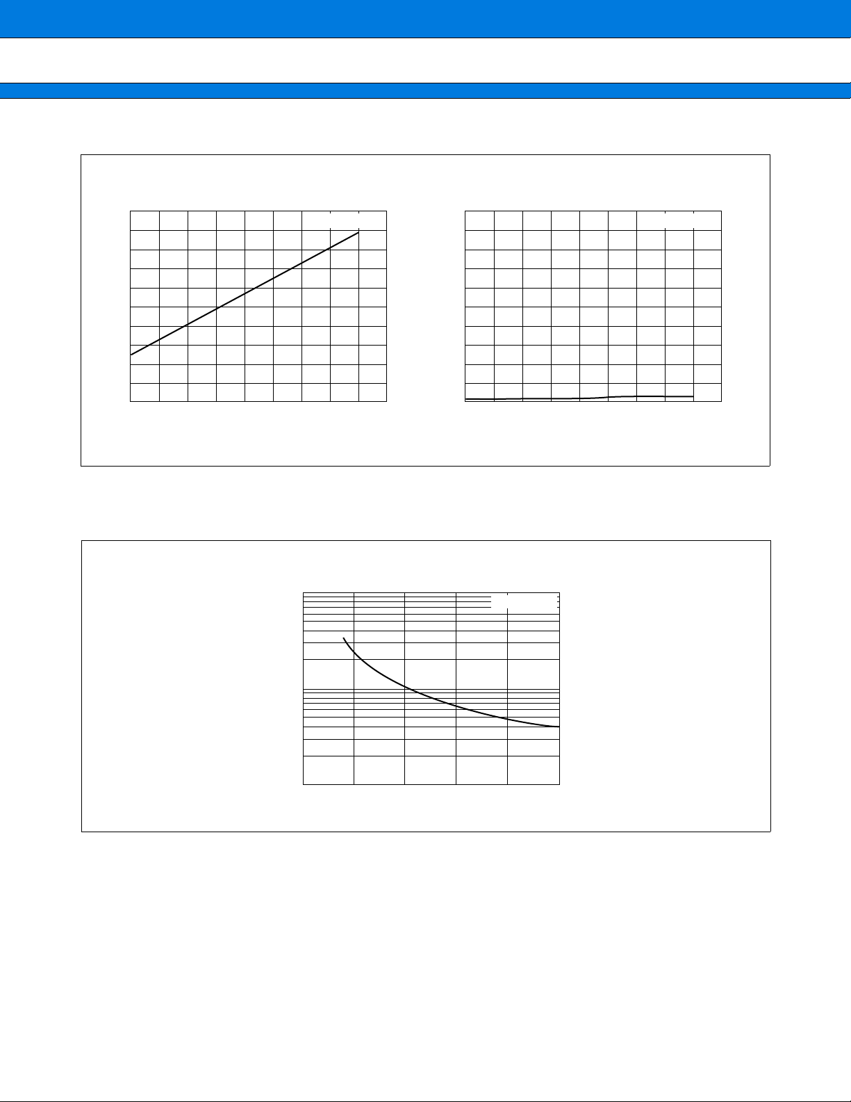
* :These values vary with the operating frequency, instruction cycle, and analog assurance range. See Figure 1
and “5. A/D Converter Electrical Characteristics.”
Figure 1 Operating Voltage vs. Main Clock Operating Frequency
6
5
Operation assurance range
4
3
Operating voltage (V)
2
Analog accuracy assured in the
AV
CC
= 3.5 V to 6.0 V range
1
1.0 2.0 3.0 4.0 5.0 6.0 7.0 8.0 9.0 10.0
Main clock operating frequency (at an instruction cycle of 4/F
4.0 2.0 0.8 0.4
Minimum execution time (instruction cycle) (µs)
Note: The shaded area is assured only for the MB89635R/636R/637R.
CH
) (MHz)
Figure 1 indicates the operating frequency of the external oscillator at an instruction cycle of 4/F
Since the operating voltage range is dependent on the instruction cycle, see minimum execution time if the
operating speed is switched using a gear.
28
CH.

MB89630R Series
WARNING: The recommended operating conditions are required in order to ensure the normal operation of the
semiconductor device. All of the device’s electrical characteristics are warranted when the device is
operated within these ranges.
Always use semiconductor devices within their recommended operating condition ranges. Operation
outside these ranges may adversely affect reliability and could result in device failure.
No warranty is made with respect to uses, operating conditions, or combinations not represented on
the data sheet. Users considering application outside the listed conditions are advised to contact their
FUJITSU representatives beforehand.
29

MB89630R Series
3. DC Characteristics
Parameter
“H” level input
voltage
“L” level input
voltage
Open-drain
output pin
application
voltage
“H” level output
voltage
“L” level output
voltage
Input leakage
current
(Hi-z output
leakage current)
Symbol
V
IH1
V
IH2
V
IHS
V
IHS2
V
IL
V
ILS
V
D
V
OH
OL
V
I
LI
Pin name Condition
P00 to P07, P10 to P17,
P22, P23, P31, P34,
P37, P41, P43,
P51 to P53
P51 to P53
RST, MOD0, MOD1,
P30, P32, P33, P35,
P36, P40, P42,P50,
P72 to P74
P50, P70, P71
P00 to P07, P10 to P17,
P22, P23, P31, P34,
P37, P41, P43
P30, P32, P33, P35,
P36, P40, P42,
P50 to P53,
P70 to P74,
RST
,
MOD0, MOD1
P50 to P53 VSS − 0.3
P00 to P07, P10 to P17,
P20 to P27, P30 to P37,
P40 to P43
P00 to P07, P10 to P17,
P20 to P27, P30 to P37,
P40 to P43, P50 to P53,
P60 to P67, RST
P00 to P07, P10 to P17,
P20 to P23, P30 to P37,
P40 to P43, P50 to P53,
P70 to P74,
MOD0, MOD1
(AVCC = VCC = 5.0 V, AVSS = VSS = 0.0 V, TA = –40°C to +85°C)
Value
Unit Remarks
Min. Typ. Max.
CC
0.7 V
0.7 VCC
0.8 VCC
0.8 VCC
VCC + 0.3
VSS + 6.0
VCC + 0.3
VSS + 6.0
V
V
V
V
V
SS − 0.3
V
SS − 0.3
0.3 VCC V
0.2 VCC V
VSS + 6.0
V
IOH = –2.0 mA 4.0 V
IOL = 4.0 mA 0.4 V
0.0 V < VI < VCC ±5 µA
P51 to P53
with pull-up
resistor
Without pull-up
resistor
P50 with
pull-up resistor
Without pull-up
resistor
Without pull-up
resistor
30
(Continued)

Parameter
Pull-up
resistance
Power supply
current
*1
Symbol
R
PULL
ICC1
CC2
I
ICCS1
I
CCS2
I
CCL
ICCLS
CCT
I
Pin name Condition
P00 to P07, P10 to P17,
P30 to P37, P40 to P43,
VI = 0.0 V 25 50 100 kΩ
P50 to P53, P72 to P74
FCH = 10 MHz
V
CC = 5.0 V
t
inst
FCH = 10 MHz
V
CC = 3.0 V
t
inst
FCL = 32.768 kHz,
VCC = 3.0 V
VCC
Subclock mode
FCL = 32.768 kHz,
VCC = 3.0 V
Subclock sleep
mode
FCL = 32.768 kHz,
VCC = 3.0 V
•Watch mode
• Ma in clock stop
mode at dualclock system
(AV
*2
= 0.4 µs
*2
= 6.4 µs
FCH = 10 MHz
V
CC = 5.0 V
*2
inst
= 0.4 µs
t
FCH = 10 MHz
V
CC = 3.0 V
Sleep mode
*2
t
inst
= 6.4 µs
MB89630R Series
CC = VCC = 5.0 V, AVSS = VSS = 0.0 V, TA = –40°C to +85°C)
Value
Min. Typ. Max.
—1220mA
—1.0 2mA
—1.52.5mA
—3 7mA
—0.51.5mA
—50100µA
—500700µA
—2550µA
—315µA
Unit Remarks
With pull-up
resistor
MB89635R/T635R/
636R/637R/T637R/
PV630
MB89P637/W637
MB89635R/T635R/
636R/637R/T637R/
PV630
MB89P637/W637
I
CCH
TA = +25°C
• Subclock stop
mode
• Ma i n clock s t o p
mode at singleclock system
—— 1µA
(Continued)
31
MB89630R Series
(Continued)
Parameter
Power supply
current
*1
Symbol
IA
I
AH
Pin name Condition
AVCC
(AVCC = VCC = 5.0 V, AVSS = VSS = 0.0 V, TA = –40°C to +85°C)
FCH = 10 MHz,
when A/D
conversion
operates.
FCH = 10 MHz,
T
A = +25°C,
when A/D
conversion in
a stop.
Value
Unit Remarks
Min. Typ. Max.
—6—mA
—— 1µA
Input capacitance C
IN
Other than AVCC,
AVSS, VCC, and VSS
f = 1 MHz — 10 — pF
*1: The power supply current is measured at the external clock.
In the case of the MB89PV630, the current consumed by the connected EPROM and ICE is not counted.
*2: For information on t
inst, see “(4) Instruction Cycle” in “4. AC Characteristics.”
4. AC Characteristics
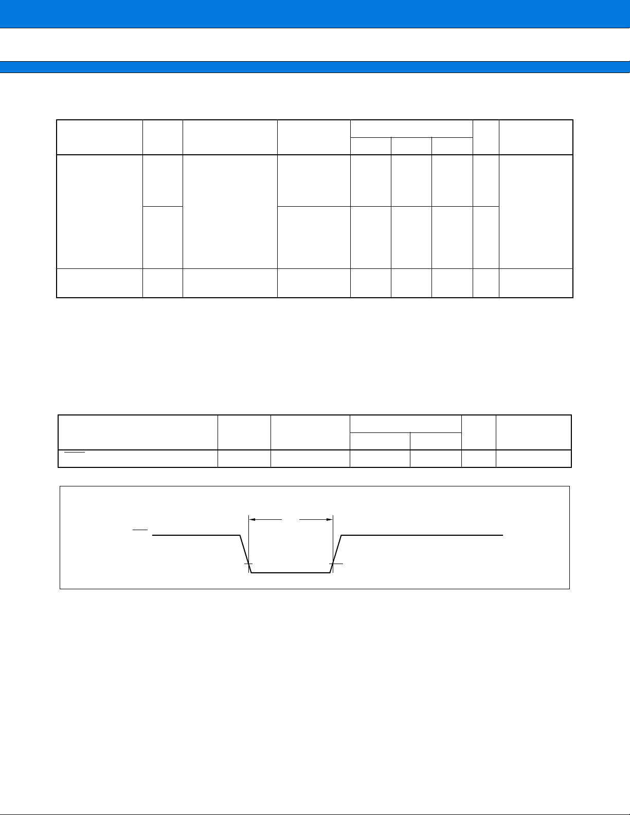
(1) Reset Timing
(VCC = 5.0 V±10%, AVSS = VSS = 0.0 V, TA = –40°C to +85°C)
Parameter
RST
“L” pulse width tZLZH — 48 tHCYL —ns
RST
Symbol Condition
tZLZH
0.2 VCC 0.2 VCC
Value
Unit Remarks
Min. Max.
32

(2) Specification for Power-on Reset
Parameter
Symbol Condition
MB89630R Series
(AVSS = VSS = 0.0 V, TA = –40°C to +85°C)
Value
Unit Remarks
Min. Max.
Power supply rising time t
Power supply cut-off time t
R
—
OFF 1—ms
— 50 ms Power-on reset function only
Min. interval time for the next
power-on reset
Note: Make sure that power supply rises within the selected oscillation stabilization time.
If power supply voltage needs to be v aried in the course of operation, a smooth voltage rise is recommended.
tOFF
0.2 V
VCC
R
t
V
2.0
0.2 V 0.2 V
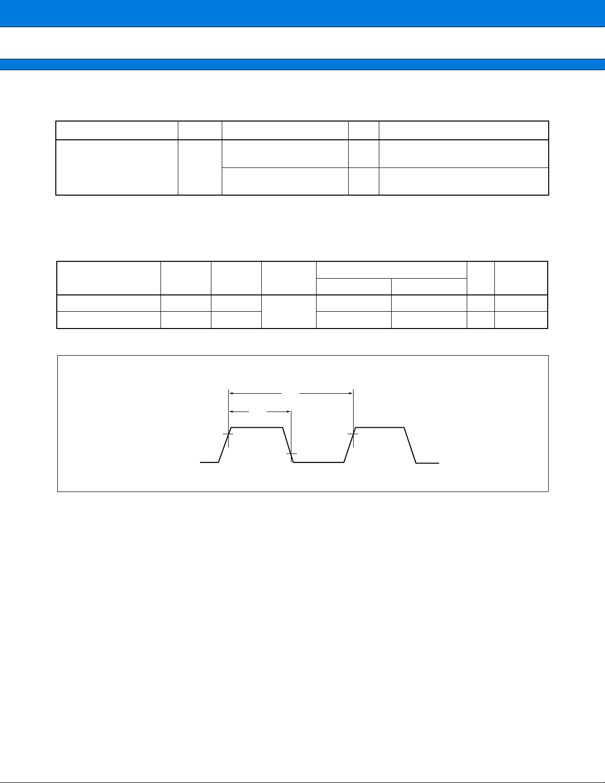
(3) Clock Timing
(AVSS = VSS = 0.0 V, TA = –40°C to +85°C)
Value
Parameter
Symbol Pin name Condition
Min. Typ. Max.
F
CH X0, X1
1—10MHz
Clock frequency
FCL X0A, X1A — 32.768 — kHz
Unit Remarks
Clock cycle time
Input clock pulse width
Input clock rising/falling
time
HCYL X0, X1 100 — 1000 ns
t
t
LCYL X0A, X1A — 30.5 — µs
PWH
PWL
WLH
P
PWLL
CR
t
tCF
X0 20 — — ns External clock
X0A — 15.2 — µs External clock
X0 — — 10 ns External clock
—
33
MB89630R Series
• Main clock timing condition
X0
• Main clock configurations
ceramic reasonator is used
0.8 VCC
tHCYL
PWL
tCF
0.2 VCC
When an external clock is used
0.2VCC
Open
PWH
tCR
0.8 VCC
0.2 VCC
When a crystal
or
X0 X1 X0 X1
• Subclock timing condition
X0A
• Subclock configurations
ceramic reasonator is used
X0A X1A
tCR
0.8 VCC
0.2 VCC
When a crystal
or
tLCYL
PWLH PWLL
tCF
0.8 VCC
0.2 VCC
When an external clock is used
X0A X1A
0.2VCC
Open
34
(4) Instruction Cycle
MB89630R Series
Parameter
Symbol Value (typical) Unit Remarks
4/FCH, 8/FCH, 16/FCH, 64/FCH µs
Instruction cycle
(minimum execution time)
t
inst
CL µs
2/F
Note: Operating at 10 MHz, the cycle varies with the set execution time.
(5) Clock Output Timing
(VCC = 5.0 V±10%, AVSS = VSS= 0.0 V, TA = –40°C to +85°C)
Parameter
Clock time t
CLK ↑ → CLK ↓ t
Symbol
CYC CLK
CHCL CLK 1/4 tinst* – 70 ns 1/4 tinst* µs
* :For information on tinst, see “(4) Instruction Cycle.”
Pin
name
Condition
Min. Max.
1/2 tinst*—µs
—
tCYC
tCHCL
CH) tinst = 0.4 µs, operating at
(4/F
F
CH = 10 MHz
inst = 61.036 µs, operating at
t
F
CL = 32.768 kHz
Value
Unit Remarks
CLK
2.4 V
2.4 V
0.8 V
35

MB89630R Series
(6) Bus Read Timing
Parameter
Valid address → RD
pulse width tRLRH
RD
↓ time tAVRL
Symbol Pin name Condition
(VCC = 5.0 V±10%, 10 MHz, AVSS = VSS= 0.0 V, TA = –40°C to +85°C)
Value
Min. Max.
RD, A15 to A08,
AD7 to AD0
RD 1/2 tinst*– 20 ns
1/4 tinst*– 64 ns
Unit Remarks
— µs
— µs
Valid address → data read
time
↓ → data read time tRLDV
RD
↑ → data hold time tRHDX
RD
↑ → ALE ↑ time tRHLH
RD
t
AVDV
RD ↑ → address loss time tRHAX
RD
↓ → CLK ↑ time tRLCH
AD7 to AD0,
A15 to A08
RD , AD7 to AD0 1/2 tinst*– 80 ns
AD7 to AD0,
RD
RD, ALE 1/4 tinst*– 40 ns
RD, A15 to A08 1/4 tinst*– 40 ns
RD, CLK
CLK ↓ → RD
RD ↓ → BUFC ↓ time tRLBL
BUFC ↑ → valid address
time
↑ time tCLRH 0—ns
RD, BUFC
A15 to A08,
BHAV
t
AD7 to AD0,
BUFC
* :For information on tinst, see “(4) Instruction Cycle.”
CLK
ALE
—
2.4 V
1/2 tinst*200µsNo wait
120 µsNo wait
0—µs
— µs
— µs
1/4 t
inst*– 40 ns
— µs
–5 — µs
5—µs
0.8 V
t
RHLH
0.8 V
36
AD
A
RD
BUFC
2.4 V
0.8 V
2.4 V
0.8 V
t
AVRL
t
AVDV
0.8 V
0.8 V
t
RLCH
t
RLDV
t
RLBL
t
RLRH
0.7 V
0.3 V
0.7 V
0.3 V
t
2.4 V
2.4V
t
0.8V
RHAX
t
CLRH
CC
CC
RHDX
CC
CC
2.4 V
0.8 V
2.4 V
0.8 V
2.4 V
t
BHAV

MB89630R Series
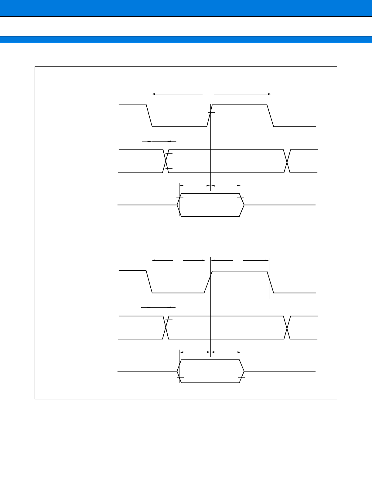
(7) Bus Write Timing
CC = 5.0 V±10%, FCH = 10 MHz, AVSS = VSS= 0.0 V, TA = –40°C to +85°C)
(V
Value
Parameter
Symbol Pin name Condition
Unit Remarks
Min. Max.
Valid address → ALE ↓ time t
ALE ↓ time → address loss
time
Valid address → WR
↓ time tAVWL WR, ALE
AVLL
AD7 to AD0,
ALE
LLAX 5—ns
t
A15 to A08
1/4 tinst*1 – 64 ns*
1/4 tinst*1 – 60 ns*
WR pulse width tWLWH WR 1/2 tinst*
Write data → WR
WR
↑ → address loss time tWHAX
↑ time tDVWH
WR ↑ → data hold time tWHDX
WR
↑ → ALE ↑ time tWHLH WR, ALE
WR
↓ → CLK ↑ time tWLCH
AD7 to AD0, WR
WR, A15 to A08
AD7 to AD0, WR
—
1/2 tinst*1 – 60 ns*
inst*
1/4 t
1/4 tinst*1 – 40 ns*
1/4 tinst*1 – 40 ns*
1/4 tinst*1 – 40 ns*
1
– 20 ns*
1
– 40 ns*
2
2
2
2
2
2
2
2
— µs
— µs
— µs
— µs
— µs
— µs
— µs
— µs
WR, CLK
CLK ↓ → WR ↑ time tCLWH 0—ns
ALE pulse width t
ALE ↓ → CLK ↑ time t
LHLL ALE 1/4 tinst*
LLCH ALE,CLK
1/4 tinst*1 – 30 ns*
1
– 35 ns*
2
2
— µs
— µs
*1: For information on tinst, see “(4) Instruction Cycle.”
*2: This characteristics are also applicable to the bus read timing.
CLK
ALE
AD
A
WR
2.4 V
2.4 V
0.8 V
2.4 V
0.8 V
tLHLL
tAVLL
2.4 V
0.8 V
tAVWL
tLLCH
0.8 V
tLLAX
2.4 V
0.8 V
tWLCH
0.8V
2.4 V
tDVWH
tWLWH
0.8 V
2.4 V
tWHLH
tWHDX
CLWH
t
tWHAX
0.8 V
2.4 V
0.8 V
2.4 V
0.8 V
37

MB89630R Series
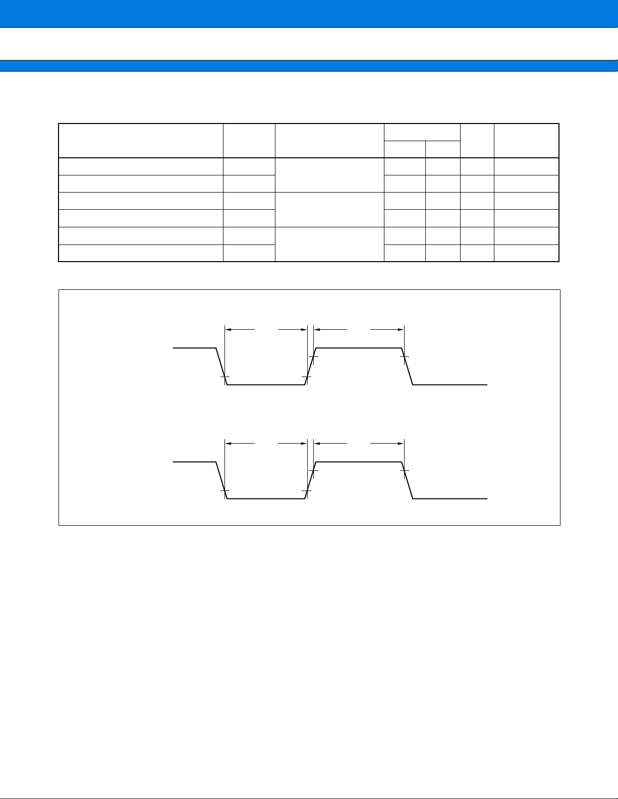
(8) Ready Input Timing
Parameter
Symbol Pin name Condition
(VCC = 5.0 V±10%, FCH = 10 MHz, AVSS = VSS= 0.0 V, TA = –40°C to +85°C)
Value
Unit Remarks
Min. Max.
RDY valid → CLK ↑ time t
YVCH
RDY, CLK —
CLK ↑ → RDY loss time t
CHYX 0—ns*
* :This characteristics are also applicable to the read cycle.
CLK
ALE
AD
A
Address Data
2.4 V
60 — ns *
2.4 V
38
WR
t
YVCH tCHYX
RDY
Note: The bus cycle is also extended in the read cycle in the same manner.
tYVCH tCHYX
(9) Serial I/O Timing
Parameter
(VCC = 5.0 V±10%, FCH = 10 MHz, AVSS = VSS= 0.0 V, TA = –40°C to +85°C)
Symbol Pin name Condition
MB89630R Series
Value
Unit Remarks
Min. Max.
Serial clock cycle time t
SCK1 ↓ → SO1 time
UCK1 ↓ → UO1 time
UCK2 ↓ → UO2 time
Valid SI1 → SCK1 ↑
Valid UI1 → UCK1 ↑
Valid UI2 → UCK2 ↑
SCK1 ↑ → valid SI1 hold time
UCK1 ↑ → valid UI1 hold time
UCK2 ↑ → valid UI2 hold time
Serial clock “H” pulse width t
Serial clock “L” pulse width t
SCK1 ↓ → SO1 time
UCK1 ↓ → UO1 time
UCK2 ↓ → UO2 time
Valid SI1 → SCK1 ↑
Valid UI1 → UCK1 ↑
Valid UI2 → UCK2 ↑
SCK1 ↓ → valid SI1 hold time
UCK1 ↓ → valid UI1 hold time
UCK2 ↓ → valid UI2 hold time
SCYC
SLOV
t
t
IVSH
t
SHIX
SHSL
SLSH
SLOV
t
t
IVSH
t
SHIX
SCK1, UCK1,
UCK2
SCK1, SO1
UCK1, UO1
UCK2, UO2
SI1, SCK1
UI1, UCK1
UI2, UCK2
SCK1, SI1
UCK1, UI1
UCK2, UI2
SCK1, UCK1,
UCK2
SCK1, UCK1,
UCK2
SCK1, SO1
UCK1, UO1
UCK2, UO2
SI1, SCK1
UI1, UCK1
UI2, UCK2
SCK1, SI1
UCK1, UI1
UCK2, UI2
Internal
shift clock
mode
External
shift clock
mode
2 t
inst*—µs
–200 200 ns
1/2 t
inst*—µs
1/2 t
inst*—µs
1 t
inst*—µs
inst*—µs
1 t
0 200 ns
1/2 t
inst*—µs
1/2 t
inst*—µs
* :For information on tinst, see “(4) Instruction Cycle.”
39
MB89630R Series
• Internal shift clock mode
tSCYC
SCK1
UCK1
UCK2
SO1
UO1
UO2
SI1
UI1
UI
• External shift clock mode
SCK1
UCK1
UCK2
2.4 V
0.8 V 0.8 V
tSLOV
2.4 V
0.8 V
0.2 VCC
tIVSH
0.8 VCC
0.2 VCC
tSLSH
0.2 VCC
tSHIX
0.8 VCC
0.8 VCC
0.2 VCC
tSHSL
0.8 VCC
40
SO1
UO1
UO2
SI1
UI1
UI
tSLOV
2.4 V
0.8 V
tIVSH tSHIX
0.8 VCC
0.2 VCC
0.8 VCC
0.2 VCC
(10) Peripheral Input Timing
Parameter
(VCC = 5.0 V±10%, AVSS = VSS = 0.0 V, TA = –40°C to +85°C)
Symbol Pin name
MB89630R Series
Value
Unit Remarks
Min. Max.
Peripheral input “H” pulse width 1 t
ILIH1
inst*— µs
2 t
PWC, INT0 to INT3,EC
Peripheral input “L” pulse width 1 tIHIL1 2 tinst*— µs
Peripheral input “H” pulse width 2 t
ILIH2
2
8
tinst*
— µs A/D mode
ADST
Peripheral input “L” pulse width 2 t
Peripheral input “H” pulse width 3 t
IHIL2
ILIH3
28 tinst*
8
tinst*
2
— µs A/D mode
— µsSense mode
ADST
Peripheral input “L” pulse width 3 t
IHIL3
28 tinst*
— µsSense mode
* :For information on tinst, see “(4) Instruction Cycle.”
PWC,
EC,
INT0 to INT3
ADST
0.2 VCC
tIHIL1
tIHIL2
(tIHIL3)
0.8 VCC
0.2
0.8 VCC
VCC
tILIH1
tILIH2
(tILIH3)
0.8 VCC
0.8 VCC
0.2 VCC
0.2
VCC
41

MB89630R Series
5. A/D Converter Electrical Characteristics
(AVCC = VCC = 3.5 V to 6.0 V, FCH = 10 MHz, AVSS = VSS = 0.0 V, TA = –40°C to +85°C)
Parameter Symbol
Pin
name
Value
Unit Remarks
Min. Typ. Max.
Resolution
——10bit
Linearity error — — ±2.0 LSB
——
Differential linearity error — — ±1.5 LSB
Total error — — ±3.0 LSB
Zero transition voltage V
OT
AVSS – 1.5 LSB AVSS + 0.5 LSB AVSS + 2.5 LSB
mV
AN0 to
Full-scale transition
voltage
Interchannel disparity
FST
V
AN7
AVR – 3.5 LSB AVR – 1.5 LSB AVR + 0.5 LSB
mV
—— 4LSB
——
A/D mode conversion time — 13.2 — µs
Analog port input current I
Analog input voltage
AIN
AN0 to
AN7
——10µA
0.0 — AVR V
—
Reference voltage
Reference voltage
supply current
R —200µA AVR = 5.0 V
—
I
0.0 — AV
CC V
At AVCC = VCC
At 10 MHz
oscillation
42

MB89630R Series
6. A/D Converter Glossary
• Resolution
Analog changes that are identifiable with the A/D converter
• Linearity error
The deviation of the straight line connecting the ze ro transition point (“00 0000 0000” ↔ “00 0000 0001”) with
the full-scale transition point (“11 1111 1110” ↔
• Differential linearity error
The deviation of input voltage needed to change the output code by 1 LSB from the theoretical value
• Total error (unit: LSB)
The difference between theoretical and actual conversion values caused by the zero transition error, full-scale
transition error, linearity error, quantization error, and noise
“11 1111 1111”) from actual conversion characteristics
3FF
3FE
3FD
004
Digital output
003
002
001
SS
AV
Theoretical I/O characteristics
VFST
VOT
1 LSB
0.5 LSB
Analog input
1 LSB =
VFST –VOT
1022
1.5 LSB
(V)
AVR
3FF
3FE
3FD
004
Digital output
003
002
001
Digital output N total error =
Actual conversion
value
{1 LSB × N + 0.5 LSB}
AV
SS
Total error
Actual conversion
value
Theoretical value
Analog input
V
NT – {1 LSB × N + 0.5 LSB}
VNT
AVR
1 LSB
(Continued)
43

MB89630R Series
(Continued)
004
003
002
Digital output
001
AVSS
Zero transition error
Actual conversion
value
V
OT (Actual measurement)
Analog input
Linearity error
Actual conversion
value
3FF
3FE
Digital output
3FD
3FC
Full-scale transition error
Theoretical value
Actual conversion
value
Actual conversion value
Analog input
Differential linearity error
FST
V
(Actual
measurement)
AVR
3FF
Actual conversion
3FE
3FD
004
Digital output
003
002
001
Digital output N linearity error =
value
{1 LSB × N + VOT}
Theoretical value
VOT (Actual measurement)
AVSS
Analog input
V
FST
(Actual
VNT
measurement)
Actual conversion value
NT – {1 LSB × N + VOT}
V
1 LSB
N + 1
Actual conversion
value
N
Digital output
N – 1
N – 2
AV
AVR
Digital output N differential linearity error =
SS
Theoretical value
VNT
Actual conversion value
Analog input
(N + 1)T –VNT
V
1 LSB
V(N + 1)T
AVR
– 1
44

MB89630R Series
7. Notes on Using A/D Converter
• Input impedance of the analog input pins
The output impedance of the external circuit for the analog input must satisfy the followingconditions.
If the output impedance of the external circuit is too high, an analog voltage sampling time might beinsufficient
(sampling time = 6 µs at 10MHz oscillation.) Therefore, it is recommended to keep the output impedance of the
external circuit below 10 kΩ .
•
Analog input circuit model
Analog input
RON2RON1
R
ON1:
Approx. 1.5 kΩ
R
Approx. 1.5 kΩ
ON2:
Approx. 60 pF
C
0:
Approx. 4 pF
C
1:
Note: The values mentioned here should be used as a guideline.
C1
•Error
The smaller the | AVR–AVss |, the greater the error would become relatively.
0
C
Converter
45

MB89630R Series
CHARACTERISTICS EXAMPLE
■
(1) “L” Level Output Voltage
OL (V)
V
VOL vs. IOL
CC = 3.0 V
V
TA = +25°C
0.5
0.4
0.3
0.2
0.1
010123456789
I
OL (mA)
V
CC = 4.0 V
V
CC = 5.0 V
V
CC = 6.0 V
(2) “H” Level Output Voltage
CC - VOH (V)
V
1.0
0.9
0.8
0.7
0.6
0.5
0.4
0.3
0.2
0.1
0.0
0.0
VCC - VOH vs. IOH
–0.5 –1.0 –1.5 –2.0 –2.5 –3.0
TA = +25°C
I
OH (mA)
(3) “H” Level Input Voltage/“L” Level Input (4) “H” Level Input Voltage/“L” Level Input
Voltage (CMOS Input)
Voltage (Hysteresis Input)
VCC = 2.5 V
V
CC = 3.0 V
VCC = 4.0 V
CC = 5.0 V
V
V
CC = 6.0 V
V
IN (V)
VIN vs. VCC
5.0
4.5
TA = +25°C
4.0
3.5
3.0
2.5
2.0
1.5
1.0
0.5
0.0
0123 456
V
7
CC (V)
V
5.0
4.5
4.0
IN (V)
VIN vs. VCC
TA = +25°C
V
IHS
3.5
3.0
2.5
2.0
VILS
1.5
1.0
0.5
0.0
0123 456
V
CC (V)
7
VIHS: Threshold as the input voltage in hysteresis
characteristics is set to “H” level
VILS: Threshold as the input voltage in hysteresis
characteristics is set to “L” level
46

(5) Power Supply Current (External Clock)
MB89630R Series
ICC (mA)
ICC1 vs. VCC, ICC2 vs. VCC
16
CH = 10MHz
14
F
TA = +25°C
12
10
8
6
4
2
0
2.5 3.0 3.5 4.0 4.5 5.0 5.5 6.0 6.5
2.0
ICCL (µA)
200
180
ICCL vs. VCC
TA = +25°C
160
140
120
100
80
60
40
20
0
2.0 2.5 3.0 3.5 4.0 4.5 5.0 5.5 6.0 6.5
Divide by 4
(I
CC1)
Divide by 8
Divide by 16
Divide by 64
(ICC2)
V
CC (V)
V
CC (V)
ICCS (mA)
ICCS1 vs. VCC, ICCS2 vs. VCC
5.0
4.5
FCH = 10MHz
TA = +25°C
4.0
3.5
3.0
2.5
2.0
1.5
1.0
0.5
0
2.0 2.5 3.0 3.5 4.0 4.5 5.0 5.5 6.0 6.5
ICCLS (µA)
50
45
ICCLS vs. VCC
TA = +25°C
40
35
30
25
20
15
10
5
0
2.0 2.5 3.0 3.5 4.0 4.5 5.0 5.5 6.0 6.5
Divide by 4
(I
CCS1)
Divide by 8
Divide by 16
Divide by 64
(I
CCS2)
V
CC (V)
V
CC (V)
(Continued)
47
MB89630R Series
(Continued)
I CCT (µA)
20
18
16
14
12
10
8
6
4
2
0
2.0 2.5 3.0 3.5 4.0 4.5 5.0 5.5 6.0 6.5
I CCT vs. V CC
TA = +25°C
(6) Pull-up Resistance
PULL (kΩ)
R
1000
V
CC (V)
R PULL vs. V CC
I CCH (µA)
2.0
1.8
1.6
1.4
1.2
1.0
0.8
0.6
0.4
0.2
0
2.0 2.5 3.0 3.5 4.0 4.5 5.0 5.5 6.0 6.5
TA = +25°C
I CCH vs. V CC
TA = +25°C
V
CC (V)
48
100
10
1
2345 6
V
CC (V)

MB89630R Series
INSTRUCTIONS (136 INSTRUCTIONS)
■
Execution instructions can be divided into the following four groups:
• Transfer
• Arithmetic operation
• Branch
•Others
Table 1 lists symbols used for notation of instructions.
Table 1 Instruction Symbols
Symbol Meaning
dir Direct address (8 bits)
off Offset (8 bits)
ext Extended address (16 bits)
#vct Vector table number (3 bits)
#d8 Immediate data (8 bits)
#d16 Immediate data (16 bits)
dir: b Bit direct address (8:3 bits)
rel Branch relative address (8 bits)
@ Register indirect (Example: @A, @IX, @EP)
A Accumulator A (Whether its length is 8 or 16 bits is determined by the instruction in use.)
AH Upper 8 bits of accumulator A (8 bits)
AL Lower 8 bits of accumulator A (8 bits)
T Temporary accumulator T (Whether its length is 8 or 16 bits is determined by the instruction in use.)
TH Upper 8 bits of temporary accumulator T (8 bits)
TL Lower 8 bits of temporary accumulator T (8 bits)
IX Index register IX (16 bits)
EP Extra pointer EP (16 bits)
PC Program counter PC (16 bits)
SP Stack pointer SP (16 bits)
PS Program status PS (16 bits)
dr Accumulator A or index register IX (16 bits)
CCR Condition code register CCR (8 bits)
RP Register bank pointer RP (5 bits)
Ri General-purpose register Ri (8 bits, i = 0 to 7)
×
( × )
(( × ))
Columns indicate the following:
Mnemonic: Assembler notation of an instruction
~: The number of instructions
#: The number of bytes
Operation: Operation of an instruction
TL, TH, AH: A content change when each of the TL, TH, and AH instructions is executed. Symbols in
N, Z, V, C: An instruction of which the corresponding flag will change. If + is written in this column,
OP code: Code of an instruction. If an instruction is more than one code, it is written according to
Indicates that the very × is the immediate data.
(Whether its length is 8 or 16 bits is determined by the instruction in use.)
Indicates that the contents of × is the target of accessing.
(Whether its length is 8 or 16 bits is determined by the instruction in use.)
The address indicated by the contents of × is the target of accessing.
(Whether its length is 8 or 16 bits is determined by the instruction in use.)
the column indicate the following:
•
“–” indicates no change.
• dH is the 8 upper bits of operation description data.
• AL and AH must become the contents of AL and AH prior to the instruction executed.
• 00 becomes 00.
the relevant instruction will change its corresponding flag.
the following rule:
Example: 48 to 4F ← This indicates 48, 49, ... 4F.
49

MB89630R Series
Table 2 T ransfer Instructions (48 instructions)
Mnemonic ~ # Operation TL TH AH N Z V C OP code
– – – –
–
–
MOV dir,A
MOV @IX +off,A
MOV ext,A
MOV @EP,A
MOV Ri,A
MOV A,#d8
MOV A,dir
MOV A,@IX +off
MOV A,ext
MOV A,@A
MOV A,@EP
MOV A,Ri
MOV dir,#d8
MOV @IX +off,#d8
MOV @EP,#d8
MOV Ri,#d8
MOVW dir,A
MOVW @IX +off,A
MOVW ext,A
MOVW @EP,A
MOVW EP,A
MOVW A,#d16
MOVW A,dir
MOVW A,@IX +off
MOVW A,ext
MOVW A,@A
MOVW A,@EP
MOVW A,EP
MOVW EP,#d16
MOVW IX,A
MOVW A,IX
MOVW SP,A
MOVW A,SP
MOV @A,T
MOVW @A,T
MOVW IX,#d16
MOVW A,PS
MOVW PS,A
MOVW SP,#d16
SWAP
SETB dir: b
CLRB dir: b
XCH A,T
XCHW A,T
XCHW A,EP
XCHW A,IX
XCHW A,SP
MOVW A,PC
(dir) ← (A)
2
3
( (IX) +off ) ← (A)
2
4
(ext) ← (A)
3
4
( (EP) ) ← (A)
1
3
(Ri) ← (A)
1
3
(A) ← d8
2
2
(A) ← (dir)
2
3
(A) ← ( (IX) +off)
2
4
(A) ← (ext)
3
4
(A) ← ( (A) )
1
3
(A) ← ( (EP) )
1
3
(A) ← (Ri)
1
3
(dir) ← d8
3
4
( (IX) +off ) ← d8
3
5
( (EP) ) ← d8
2
4
(Ri) ← d8
2
4
(dir) ← (AH),(dir + 1) ← (AL)
2
4
( (IX) +off) ← (AH),
2
5
( (IX) +off + 1) ← (AL)
(ext) ← (AH), (ext + 1) ← (AL)
3
5
( (EP) ) ← (AH),( (EP) + 1) ← (AL)
1
4
(EP) ← (A)
1
2
(A) ← d16
3
3
(AH) ← (dir), (AL) ← (dir + 1)
2
4
(AH) ← ( (IX) +off),
2
5
(AL) ← ( (IX) +off + 1)
(AH) ← (ext), (AL) ← (ext + 1)
3
5
(AH) ← ( (A) ), (AL) ← ( (A) ) + 1)
1
4
(AH) ← ( (EP) ), (AL) ← ( (EP) + 1)
1
4
(A) ← (EP)
1
2
(EP) ← d16
3
3
(IX) ← (A)
1
2
(A) ← (IX)
1
2
(SP) ← (A)
1
2
(A) ← (SP)
1
2
( (A) ) ← (T)
1
3
( (A) ) ← (TH),( (A) + 1) ← (TL)
1
4
(IX) ← d16
3
3
(A) ← (PS)
1
2
(PS) ← (A)
1
2
(SP) ← d16
3
3
(AH) ↔ (AL)
1
2
(dir): b ← 1
2
4
(dir): b ← 0
2
4
(AL) ↔ (TL)
1
2
(A) ↔ (T)
1
3
(A) ↔ (EP)
1
3
(A) ↔ (IX)
1
3
(A) ↔ (SP)
1
3
(A) ← (PC)
1
2
–
–
–
–
–
AL
AL
AL
AL
AL
AL
AL
–
–
–
–
–
–
–
–
–
AL
AL
AL
AL
AL
AL
–
–
–
–
–
–
–
–
–
–
–
–
–
–
–
AL
AL
–
–
–
–
–
–
–
–
–
–
–
–
–
–
–
–
–
–
–
–
–
–
–
–
AH
AH
AH
AH
AH
AH
–
–
–
–
–
–
–
–
–
–
–
–
–
–
–
–
AH
–
–
–
–
–
–
–
–
–
–
–
–
–
–
–
–
–
–
–
–
–
–
–
–
dH
dH
dH
dH
dH
dH
dH
–
–
dH
–
dH
–
–
–
dH
–
–
AL
–
–
–
dH
dH
dH
dH
dH
– – – –
– – – –
– – – –
– – – –
+ + – –
+ + – –
+ + – –
+ + – –
+ + – –
+ + – –
+ + – –
– – – –
– – – –
– – – –
– – – –
– – – –
– – – –
– – – –
– – – –
– – – –
+ + – –
+ + – –
+ + – –
+ + – –
+ + – –
+ + – –
– – – –
– – – –
– – – –
– – – –
– – – –
– – – –
– – – –
– – – –
– – – –
– – – –
+ + + +
– – – –
– – – –
– – – –
– – – –
– – – –
– – – –
– – – –
– – – –
– – – –
– – – –
45
46
61
47
48 to 4F
04
05
06
60
92
07
08 to 0F
85
86
87
88 to 8F
D5
D6
D4
D7
E3
E4
C5
C6
C4
93
C7
F3
E7
E2
F2
E1
F1
82
83
E6
70
71
E5
10
A8 to AF
A0 to A7
42
43
F7
F6
F5
F0
Note: During byte transfer to A, T
Operands in more than one operand instruction must be stored in the order in which their mnemonics
are written. (Reverse arrangement of F
50
← A is restricted to low bytes.
2
MC-8 family)

MB89630R Series
Table 3 Arithmetic Operation Instructions (62 instructions)
Mnemonic ~ # Operation TL TH AH N Z V C OP code
ADDC A,Ri
ADDC A,#d8
ADDC A,dir
ADDC A,@IX +off
ADDC A,@EP
ADDCW A
ADDC A
SUBC A,Ri
SUBC A,#d8
SUBC A,dir
SUBC A,@IX +off
SUBC A,@EP
SUBCW A
SUBC A
INC Ri
INCW EP
INCW IX
INCW A
DEC Ri
DECW EP
DECW IX
DECW A
MULU A
DIVU A
ANDW A
ORW A
XORW A
CMP A
CMPW A
RORC A
3
2
3
4
3
3
2
3
2
3
4
3
3
2
4
3
3
3
4
3
3
3
19
21
3
3
3
2
3
2
1
(A) ← (A) + (Ri) + C
2
(A) ← (A) + d8 + C
2
(A) ← (A) + (dir) + C
2
(A) ← (A) + ( (IX) +off) + C
1
(A) ← (A) + ( (EP) ) + C
1
(A) ← (A) + (T) + C
1
(AL) ← (AL) + (TL) + C
1
(A) ← (A) − (Ri) − C
2
(A) ← (A) − d8 − C
2
(A) ← (A) − (dir) − C
2
(A) ← (A) − ( (IX) +off) − C
1
(A) ← (A) − ( (EP) ) − C
1
(A) ← (T) − (A) − C
1
(AL) ← (TL) − (AL) − C
1
(Ri) ← (Ri) + 1
1
(EP) ← (EP) + 1
1
(IX) ← (IX) + 1
1
(A) ← (A) + 1
1
(Ri) ← (Ri) − 1
1
(EP) ← (EP) − 1
1
(IX) ← (IX) − 1
1
(A) ← (A) − 1
1
(A) ← (AL) × (TL)
1
(A) ← (T) / (AL),MOD → (T)
1
(A) ← (A) ∧ (T)
1
(A) ← (A) ∨ (T)
1
(A) ← (A) ∀ (T)
1
1
1
(TL) − (AL)
(T) − (A)
→→
A
C
–
–
–
–
–
–
–
–
–
–
–
–
–
–
–
–
–
–
–
–
–
–
–
dL
–
–
–
–
–
–
–
–
–
–
–
–
–
–
–
–
–
–
–
–
–
–
–
–
–
–
–
–
–
00
–
–
–
–
–
–
–
–
–
–
–
dH
–
–
–
–
–
–
dH
–
–
–
–
dH
–
–
–
dH
dH
00
dH
dH
dH
–
–
–
+ + + +
+ + + +
+ + + +
+ + + +
+ + + +
+ + + +
+ + + +
+ + + +
+ + + +
+ + + +
+ + + +
+ + + +
+ + + +
+ + + +
+ + + –
– – – –
– – – –
+ + – –
+ + + –
– – – –
– – – –
+ + – –
– – – –
– – – –
+ + R –
+ + R –
+ + R –
+ + + +
+ + + +
+ + – +
28 to 2F
24
25
26
27
23
22
38 to 3F
34
35
36
37
33
32
C8 to CF
C3
C2
C0
D8 to DF
D3
D2
D0
01
11
63
73
53
12
13
03
ROLC A
CMP A,#d8
CMP A,dir
CMP A,@EP
CMP A,@IX +off
CMP A,Ri
DAA
DAS
XOR A
XOR A,#d8
XOR A,dir
XOR A,@EP
XOR A,@IX +off
XOR A,Ri
AND A
AND A,#d8
AND A,dir
←
←
AC
2
1
2
2
3
2
3
1
4
2
3
1
2
2
2
2
3
3
4
3
2
2
3
Decimal adjust for addition
1
Decimal adjust for subtraction
1
(A) ← (AL) ∀ (TL)
1
(A) ← (AL) ∀ d8
2
(A) ← (AL) ∀ (dir)
2
(A) ← (AL) ∀ ( (EP) )
1
(A) ← (AL) ∀ ( (IX) +off)
2
(A) ← (AL) ∀ (Ri)
1
(A) ← (AL) ∧ (TL)
1
(A) ← (AL) ∧ d8
2
(A) ← (AL) ∧ (dir)
2
(A) − d8
(A) − (dir)
(A) − ( (EP) )
(A) − ( (IX) +off)
(A) − (Ri)
–
–
–
+ + – +
–
–
–
+ + + +
–
–
–
+ + + +
–
–
–
+ + + +
–
–
–
+ + + +
–
–
–
+ + + +
–
–
–
+ + + +
–
–
–
+ + + +
–
–
–
+ + R –
–
–
–
+ + R –
–
–
–
+ + R –
–
–
–
+ + R –
–
–
–
+ + R –
–
–
–
+ + R –
–
–
–
+ + R –
–
–
–
+ + R –
–
–
–
+ + R –
02
14
15
17
16
18 to 1F
84
94
52
54
55
57
56
58 to 5F
62
64
65
(Continued)
51

MB89630R Series
(Continued)
Mnemonic ~ # Operation TL TH AH N Z V C OP code
AND A,@EP
AND A,@IX +off
AND A,Ri
OR A
OR A,#d8
OR A,dir
OR A,@EP
OR A,@IX +off
OR A,Ri
CMP dir,#d8
CMP @EP,#d8
CMP @IX +off,#d8
CMP Ri,#d8
INCW SP
DECW SP
Mnemonic ~ # Operation TL TH AH N Z V C OP code
BZ/BEQ rel
BNZ/BNE rel
BC/BLO rel
BNC/BHS rel
BN rel
BP rel
BLT rel
BGE rel
BBC dir: b,rel
BBS dir: b,rel
JMP @A
JMP ext
CALLV #vct
CALL ext
XCHW A,PC
RET
RETI
3
1
(A) ← (AL) ∧ ( (EP) )
4
2
(A) ← (AL) ∧ ( (IX) +off)
3
1
(A) ← (AL) ∧ (Ri)
2
1
(A) ← (AL) ∨ (TL)
2
2
(A) ← (AL) ∨ d8
3
2
(A) ← (AL) ∨ (dir)
3
1
(A) ← (AL) ∨ ( (EP) )
4
2
(A) ← (AL) ∨ ( (IX) +off)
3
1
(A) ← (AL) ∨ (Ri)
5
3
4
2
5
3
4
2
3
1
(SP) ← (SP) + 1
3
1
(SP) ← (SP) – 1
Table 4 Branch Instructions (17 instructions)
3
2
If Z = 1 then PC ← PC + rel
3
2
If Z = 0 then PC ← PC + rel
3
2
If C = 1 then PC ← PC + rel
3
2
If C = 0 then PC ← PC + rel
3
2
If N = 1 then PC ← PC + rel
3
2
If N = 0 then PC ← PC + rel
3
2
If V ∀ N = 1 then PC ← PC + rel
3
2
If V ∀ N = 0 then PC ← PC + reI
5
3
If (dir: b) = 0 then PC ← PC + rel
5
3
If (dir: b) = 1 then PC ← PC + rel
2
1
(PC) ← (A)
3
3
(PC) ← ext
6
1
Vector call
6
3
Subroutine call
3
1
(PC) ← (A),(A) ← (PC) + 1
4
1
Return from subrountine
6
1
Return form interrupt
(dir) – d8
( (EP) ) – d8
( (IX) + off) – d8
(Ri) – d8
–
–
–
+ + R –
–
–
–
+ + R –
–
–
–
+ + R –
–
–
–
+ + R –
–
–
–
+ + R –
–
–
–
+ + R –
–
–
–
+ + R –
–
–
–
+ + R –
–
–
–
+ + R –
–
–
–
+ + + +
–
–
–
+ + + +
–
–
–
+ + + +
–
–
–
+ + + +
–
–
–
– – – –
–
–
–
– – – –
–
–
–
– – – –
–
–
–
– – – –
–
–
–
– – – –
–
–
–
– – – –
–
–
–
– – – –
–
–
–
– – – –
–
–
–
– – – –
–
–
–
– – – –
–
–
–
– + – –
–
–
–
– + – –
–
–
–
– – – –
–
–
–
– – – –
–
–
–
– – – –
–
–
–
– – – –
–
–
dH
– – – –
–
–
–
– – – –
–
–
–
Restore
67
66
68 to 6F
72
74
75
77
76
78 to 7F
95
97
96
98 to 9F
C1
D1
FD
FC
F9
F8
FB
FA
FF
FE
B0 to B7
B8 to BF
E0
21
E8 to EF
31
F4
20
30
PUSHW A
POPW A
PUSHW IX
POPW IX
NOP
CLRC
SETC
CLRI
SETI
52
Table 5 Other Instructions (9 instructions)
Mnemonic ~ # Operation TL TH AH N Z V C OP code
4
1
4
1
4
1
4
1
1
1
1
1
1
1
1
1
1
1
–
–
–
– – – –
–
–
dH
– – – –
–
–
–
– – – –
–
–
–
– – – –
–
–
–
– – – –
–
–
–
– – – R
–
–
–
– – – S
–
–
–
– – – –
–
–
–
– – – –
40
50
41
51
00
81
91
80
90

INSTRUCTION MAP
■
A,SP
A,PC
MOVW
MOVW
@A
SP,A
JMP
MOVW
A
SP
DECW
DECW
A
SP
INCW
INCW
dir: 0,rel
BBC
dir: 1,rel
BBC
dir: 0
dir: 1
A,IX
MOVW
IX,A
MOVW
IX
DECW
IX
INCW
dir: 2,rel
BBC
dir: 2
CLRB
A,EP
MOVW
EP,A
MOVW
EP
DECW
EP
INCW
dir: 3,rel
BBC
dir: 3
CLRB
A,PC
XCHW
A,#d16
MOVW
ext,A
MOVW
A,ext
MOVW
dir: 4,rel
BBC
dir: 4
A,SP
XCHW
SP,#d16
MOVW
dir,A
MOVW
A,dir
MOVW
dir: 5,rel
BBC
dir: 5
CLRB
A,IX
XCHW
IX,#d16
MOVW
@IX +d,A
MOVW
A,@IX +d
MOVW
dir: 6,rel
BBC
dir: 6
CLRB
A,EP
XCHW
EP,#d16
MOVW
@EP,A
MOVW
A,@EP
MOVW
dir: 7,rel
BBC
dir: 7
CLRB
rel
BNC
#0
CALLV
R0
DEC
R0
INC
dir: 0,rel
BBS
dir: 0
SETB
MB89630R Series
rel
rel
rel
rel
rel
BC
BP
BN
BNZ
BZ
BGE
#1
#2
CALLV
R1
DEC
R1
INC
dir: 1,rel
BBS
dir: 1
SETB
CALLV
R2
DEC
R2
INC
dir: 2,rel
BBS
dir: 2
SETB
#3
CALLV
R3
DEC
R3
INC
dir: 3,rel
BBS
dir: 3
SETB
CALLV
DEC
INC
BBS
SETB
#4
R4
R4
dir: 4,rel
dir: 4
#5
CALLV
R5
DEC
R5
INC
dir: 5,rel
BBS
dir: 5
SETB
CALLV
DEC
INC
BBS
SETB
rel
#6
R6
R6
dir: 6,rel
dir: 6
rel
BLT
#7
CALLV
R7
DEC
R7
INC
dir: 7,rel
BBS
dir: 7
SETB
0123456789ABCDEF
H
L
CLRI SETI CLRB
A,PS
MOVW
A,ext
MOV
A
POPW
A
NOP SWAP RET RETI PUSHW
0
CLRC SETC CLRB
PS,A
MOVW
ext,A
MOV
IX
POPW
IX
PUSHW
addr16
CALL
addr16
JMP
A
DIVU
A
MULU
1
A,@A
MOV
@A,T
MOV
A
OR
A
AND
A
XOR
A, T
XCH
A
SUBC
A
ADDC
A
CMP
A
ROLC
2
A,@A
MOVW
@A,T
MOVW
A
ORW
A
ANDW
A
XORW
A, T
XCHW
A
SUBCW
A
ADDCW
A
CMPW
A
RORC
3
DAA DAS CLRB
A,#d8
OR
A,#d8
AND
A,#d8
XOR
A,#d8
SUBC
A,#d8
ADDC
A,#d8
CMP
A,#d8
MOV
4
dir,#d8
CMP
dir,#d8
MOV
A,dir
OR
A,dir
AND
A,dir
XOR
dir,A
MOV
A,dir
SUBC
A,dir
ADDC
A,dir
CMP
A,dir
MOV
5
CMP
@IX +d,#d8
@IX +d,#d8
MOV
OR
A,@IX +d
AND
A,@IX +d
A,@IX +d
XOR
MOV
@IX +d,A
SUBC
A,@IX +d
ADDC
A,@IX +d
CMP
A,@IX +d
MOV
A,@IX +d
6
CMP
@EP,#d8
MOV
@EP,#d8
A,@EP
OR
A,@EP
AND
A,@EP
XOR
@EP,A
MOV
A,@EP
SUBC
A,@EP
ADDC
A,@EP
CMP
A,@EP
MOV
7
R0,#d8
CMP
R0,#d8
MOV
A,R0
OR
A,R0
AND
A,R0
XOR
R0,A
MOV
A,R0
SUBC
A,R0
ADDC
A,R0
CMP
A,R0
MOV
8
R1,#d8
CMP
R1,#d8
MOV
A,R1
OR
A,R1
AND
A,R1
XOR
R1,A
MOV
A,R1
SUBC
A,R1
ADDC
A,R1
CMP
A,R1
MOV
9
R2,#d8
CMP
R2,#d8
MOV
A,R2
OR
A,R2
AND
A,R2
XOR
R2,A
MOV
A,R2
SUBC
A,R2
ADDC
A,R2
CMP
A,R2
MOV
A
R3,#d8
CMP
R3,#d8
MOV
A,R3
OR
A,R3
AND
A,R3
XOR
R3,A
MOV
A,R3
SUBC
A,R3
ADDC
A,R3
CMP
A,R3
MOV
B
R4,#d8
CMP
R4,#d8
MOV
A,R4
OR
A,R4
AND
A,R4
XOR
R4,A
MOV
A,R4
SUBC
A,R4
ADDC
A,R4
CMP
A,R4
MOV
C
R5,#d8
CMP
R5,#d8
MOV
A,R5
OR
A,R5
AND
A,R5
XOR
R5,A
MOV
A,R5
SUBC
A,R5
ADDC
A,R5
CMP
A,R5
MOV
D
R6,#d8
CMP
R6,#d8
MOV
A,R6
OR
A,R6
AND
A,R6
XOR
R6,A
MOV
A,R6
SUBC
A,R6
ADDC
A,R6
CMP
A,R6
MOV
E
R7,#d8
CMP
R7,#d8
MOV
A,R7
OR
A,R7
AND
A,R7
XOR
R7,A
MOV
A,R7
SUBC
A,R7
ADDC
A,R7
CMP
A,R7
MOV
F
53

MB89630R Series
MASK OPTIONS
■
Part number
No.
Specifying procedure
Pull-up resistors
P00 to P07, P10 to P17,
1
P30 to P37, P40 to P43,
P50 to P53, P72 to P74
Power-on reset selection
2
With power-on reset
Without power-on reset
Selection of the main clock
oscillation stabilization time
(at 10 MHz)
18
Approx. 2
3
Approx. 2
Approx. 2
Approx. 2
F
CH : Main clock frequency
/FCH (Approx. 26.2 ms)
17
/FCH (Approx. 13.1 ms)
14
/FCH (Approx. 1.6 ms)
4
/FCH (Approx. 0 ms)
Reset pin output
4
Reset output provided
No reset output
Single/dual-clock system option
Single clock
Dual clock
5
MB89635R
MB89636R
MB89637R
Specify when
ordering
masking
Selectable by
pin
MB89P637
MB89W637
Set with EPROM
programmer
Can be set per pin*
MB89PV630
MB89T635R
MB89T637R
Setting not possible
Fixed to “without pull-up
resistor”
Selectable Setting possible Fixed to “with power-on reset”
18
Selectable Setting possible
Fixed to 2
(Approx. 26.2 ms)
/FCH
Selectable Setting possible Fixed to “with reset output”
MB89PV630-101 Single-clock system
MB89T635R-101 Single-clock system
Selectable Setting possible
MB89T637R-101 Single-clock system
MB89PV630-102 Dual-clock systems
MB89T635R-102 Dual-clock systems
MB89T637R-102 Dual-clock systems
* :Pull-up resistors cannot be set for P50 to P53.
54

ORDERING INFORMATION
■
Part number Package Remarks
MB89635RP-SH
MB89T635RP-SH
MB89636RP-SH
MB89637RP-SH
MB89P637P-SH
MB89T637RP-SH
MB89635RPF
MB89T635RPF
MB89636RPF
MB89637RPF
MB89P637PF
MB89T637RPF
MB89635RPFM
MB89636RPFM
MB89637RPFM
MB89T635PFM
MB89630R Series
64-pin Plastic SH-DIP
(DIP-64P-M01)
64-pin Plastic QFP
(FPT-64P-M06)
64-pin Plastic QFP
(FPT-64P-M09)
MB89W637C-SH
MB89PV630CF
MB89PV630C-SH
64-pin Ceramic SH-DIP
(DIP-64C-A06)
64-pin Ceramic MQFP
(MQP-64C-P01)
64-pin Ceramic MDIP
(MDP-64C-P02)
55

MB89630R Series
PACKAGE DIMENSIONS
■
64-pin Plastic SH-DIP
(DIP-64P-M01)
58.00
2.283
+0.22
–0.55
+.008
–.022
INDEX-1
INDEX-2
5.65(.222)MAX
3.00(.118)MIN
+0.50
–0
1.00
+.020
–0
.039
1.778±0.18
1.778(.070)
MAX
C
1994 FUJITSU LIMITED D64001S-3C-4
(.070±.007)
64-pin Plastic QFP
(FPT-64P-M06)
51
24.70±0.40(.972±.016)
20.00±0.20(.787±.008)
0.45±0.10
(.018±.004)
55.118(2.170)REF
17.00±0.25
(.669±.010)
0.25±0.05
(.010±.002)
0.51(.020)MIN
15°MAX
19.05(.750)
TYP
Dimensions in mm (inches)
3.35(.132)MAX
33
(Mounting height)
0.05(.002)MIN
(STAND OFF)
56
52 32
64
LEAD No.
C
1994 FUJITSU LIMITED F64013S-3C-2
1
INDEX
1.00(.0394)
TYP (.016±.004)
0.10(.004)
18.00(.709)REF
22.30±0.40(.878±.016)
0.40±0.10
"A"
19
0.20(.008)
14.00±0.20
(.551±.008)
20
M
"B"
18.70±0.40
(.736±.016)
Details of "A" part
0.18(.007)MAX
0.63(.025)MAX
12.00(.472)
REF
0.15±0.05(.006±.002)
0.25(.010)
0.30(.012)
Details of "B" part
Dimensions in mm (inches)
16.30±0.40
(.642±.016)
0 10°
1.20±0.20
(.047±.008)

64-pin Plastic QFP
(FPT-64P-M09)
48 33
49
14.00±0.20(.551±.008)SQ
12.00±0.10(.472±.004)SQ
1 PIN INDEX
MB89630R Series
+0.20
1.50
–0.10
(Mounting height)
+.008
–.004
.059
32
9.75
13.00
(.512)
(.384)
NOM
REF
64
LEAD No.
0.65(.0256)TYP
C
1994 FUJITSU LIMITED F64018S-1C-2
64-pin Ceramic SH-DIP
(DIP-64C-A06)
R1.27(.050)
REF
INDEX AREA
0.30±0.10
(.012±.004)
0.10(.004)
56.90±0.56
(2.240±.022)
161
0.13(.005)
17
"A"
M
8.89(.350) DIA
TYP
0.127
.005
+0.05
–0.02
+.002
–.001
Details of "A" part
0.10±0.10
(.004±.004)
0.50±0.20
0 10°
(.020±.008)
Dimensions in mm (inches)
18.75±0.25
(.738±.010)
(STAND OFF)
5.84(.230)MAX
3.40±0.36
(.134±.014)
1.45(.057)
MAX
C
1994 FUJITSU LIMITED D64006SC-1-2
1.778±0.180
(.070±.007)
55.118(2.170)REF
0.90±0.10
(.0355±.0040)
0.46
.018
+0.13
–0.08
+.005
–.003
1.27±0.25
(.050±.010)
0.25±0.05
(.010±.004)
19.05±0.25
(.750±.010)
Dimensions in mm (inches)
0°~9°
57

MB89630R Series
64-pin Ceramic MQFP
(MQP-64C-P01)
INDEX AREA
(.050±.005)
22.30±0.33
(.878±.013)
24.70(.972)
TYP
1.27±0.13
0.30(.012)
TYP
18.70(.736)TYP
16.30±0.33
(.642±.013)
15.58±0.20
(.613±.008)
12.02(.473)
10.16(.400)
TYP
TYP
14.22(.560)
18.12±0.20
(.713±.008)
TYP
1.20
.047
+0.40
–0.20
+.016
–.008
12.00(.472)TYP
1.00±0.25
(.039±.010)
1.00±0.25
(.039±.010)
18.00(.709)
TYP
1.27±0.13
(.050±.005)
0.50(.020)TYP
C
1994 FUJITSU LIMITED M64004SC-1-3
64-pin Ceramic MDIP
(MDP-64C-P02)
15.24(.600)
TYP
INDEX AREA
33.02(1.300)REF
0.30(.012)TYP
7.62(.300)TYP
9.48(.373)TYP
11.68(.460)TYP
0.15±0.05
(.006±.002)
56.90±0.64
(2.240±.025)
2.54±0.25
(.100±.010)
10.82(.426)
MAX
0.40±0.10
(.016±.004)
0.40±0.10
(.016±.004)
Dimensions in mm (inches)
18.75±0.30
(.738±.012)
0.25±0.05
(.010±.002)
+0.40
–0.20
1.20
+.016
–.008
.047
0°~9°
19.05±0.30
(.750±.012)
58
10.16(.400)MAX
+0.13
0.46
1.778±0.25
(.070±.010)
C
1994 FUJITSU LIMITED M64002SC-1-4
–0.08
+.005
–.003
.018
55.12(2.170)REF
0.90±0.13
(.035±.005)
1.27±0.25
(.050±.010)
3.43±0.38
(.135±.015)
Dimensions in mm (inches)

FUJITSU LIMITED
For further information please contact:
MB89630R Series
Japan
FUJITSU LIMITED
Corporate Global Business Support Division
Electronic Devices
KAWASAKI PLANT, 4-1-1, Kamikodanaka,
Nakahara-ku, Kawasaki-shi,
Kanagawa 211-8588, Japan
Tel: +81-44-754-3763
Fax: +81-44-754-3329
http://www.fujitsu.co.jp/
North and South America
FUJITSU MICROELECTRONICS, INC.
3545 North First Street,
San Jose, CA 95134-1804, USA
Tel: +1-408-922-9000
Fax: +1-408-922-9179
Customer Response Center
Mon. - Fri.: 7 am - 5 pm (PST)
Tel: +1-800-866-8608
Fax: +1-408-922-9179
http://www.fujitsumicro.com/
Europe
FUJITSU MICROELECTRONICS EUR OPE GmbH
Am Siebenstein 6-10,
D-63303 Dreieich-Buchschlag,
Germany
Tel: +49-6103-690-0
Fax: +49-6103-690-122
http://www.fujitsu-fme.com/
Asia Pacific
FUJITSU MICROELECTRONICS ASIA PTE LTD
#05-08, 151 Lorong Chuan,
New Tech Park,
Singapore 556741
Tel: +65-281-0770
Fax: +65-281-0220
http://www.fmap.com.sg/
All Rights Reserved.
The contents of this document are subject to change without
notice.
Customers are advised to consult with FUJITSU sales
representatives before ordering.
The information and circuit diagrams in this document are
presented as examples of semiconductor device applications,
and are not intended to be incorporated in devices for actual use.
Also, FUJITSU is unable to assume responsibility for
infringement of any patent rights or other rights of third parties
arising from the use of this information or circuit diagrams.
The contents of this document may not be reproduced or copied
without the permission of FUJITSU LIMITED.
FUJITSU semiconductor devices are intended for use in
standard applications (computers, office automation and other
office equipments, industrial, communications, and
measurement equipments, personal or household devices, etc.).
CAUTION:
Customers considering the use of our products in special
applications where failure or abnormal operation may directly
affect human lives or cause physical injury or property damage,
or where extremely high levels of reliability are demanded
(such as aerospace systems, atomic energy controls, sea floor
repeaters, vehicle operating controls, medical devices for life
support, etc.) are requested to consult with FUJITSU sales
representatives before such use. The company will not be
responsible for damages arising from such use without prior
approval.
Any semiconductor devices have inherently a certain rate of
failure. You must protect against injury, damage or loss from
such failures by incorporating safety design measures into your
facility and equipment such as redundancy, fire protection, and
prevention of over-current levels and other abnormal operating
conditions.
If any products described in this document represent goods or
technologies subject to certain restrictions on export under the
Foreign Exchange and Foreign Trade Control Law of Japan, the
prior authorization by Japanese government should be required
for export of those products from Japan.
F9609
FUJITSU LIMITED Printed in Japan
59
 Loading...