

查询MB89490_03供应商
FUJITSU SEMICONDUCTOR
DATA SHEET
8-bit Proprietary Microcontroller
CMOS
F2MC-8L MB89490 Series
MB89498/F499/PV490
DESCRIPTION
■
The MB89490 series has been developed as a general-purpose version of the F2MC*-8L family consisting of
proprietary 8-bit single-chip microcontrollers.
DS07-12560-1E
In addition to a compact instruction set, the general-purpose, single-chip microcontroller contains a variety of
peripheral functions such as 21-bit timebase timer, watch prescaler, PWM timer, 8/16-bit timer/counter, remote
receiver circuit, LCD controller/driver, e xternal interrupt 0 (edge) , external interrupt 1 (level) , 10-bit A/D converter,
UART/SIO, SIO, I
The MB89490 series is designed suitable for compact disc/radio receiver controller as well as in a wide range of
applications for consumer product.
2
* : “F
MC”, an abbreviation for FUJITSU Flexible Microcontroller, is a registered trademark of FUJITSU Ltd.
FEATURES
■
• Package
QFP, LQFP package for MB89F499, MB89498
MQFP package for MB89PV490
PACKAGES
■
100-pin Plastic QFP 100-pin Plastic LQFP 100-pin Ceramic MQFP
2
C and watchdog timer reset.
(Continued)
(FTP-100P-M06) (FTP-100P-M05) (MQP-100C-P01)

MB89490 Series
(Continued)
• High speed operating capability at low voltage
• Minimum execution time : 0.32 µs/12.5 MHz
2
•F
MC-8L family CPU core
Multiplication and division instructions
Instruction set optimized for controllers
• PLL circuit for sub-clock
• Embedded for PLL clock multiplication circuit for sub-clock
• Operating clock (PLL for sub-clock) can be selected from no multiplication or 4 times of the sub-clock
oscillation frequency.
•6 timers
PWM timer × 2
8/16-bit timer/counter × 2
21-bit timebase timer
Watch prescaler
• External interrupt
Edge detection (selectable edge) : 8 channels
Low level interrupt (wake-up function) : 8 channels
• 10-bit A/D converter (8 channels)
10-bit successive approximation type
• UART/SIO
Synchronous/asynchronous data transfer capability
•SIO
Switching of synchronous data transfer capability
• LCD controller/driver
Max 32 segments output × 4 commons
2
•I
C interface circuit
• Remote receiver circuit
• Low-power consumption mode
Stop mode (oscillation stops so as to minimize the current consumption.)
Sleep mode (CPU stops so as to reduce the current consumption to approx. 1/3 of normal.)
Watch mode (operation except the watch prescaler stops so as to reduce the power comsumption to an
extremely low level.)
Sub-clock mode
• Watchdog timer reset
• I/O ports : Max 66 channels
16-bit arithmetic operations
Branch instructions by test bit
Bit manipulation instructions, etc.
2
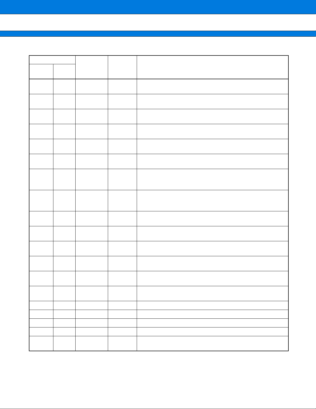
PRODUCT LINEUP
■
MB89490 Series
Part number
Parameter
Classification
ROM size
RAM size 2 K × 8-bit 2 K × 8-bit 2 K × 8-bit
CPU functions
Ports
21-bit timebase
timer
Watchdog timer Reset generation cycle (167.8 ms to 335.5 ms) at 12.5 MHz
Mass production products
Number of instructions
Instruction bit length
Instruction length
Data bit length
Minimum instruction execution time
Minimum interrupt processing time
General-purpose I/O ports (CMOS)
Input ports (CMOS)
N-channel open drain I/O ports
Total
Interrupt generation cycle (0.66 ms, 2.6 ms, 21.0 ms, 335.5 ms) at 12.5 MHz
MB89498 MB89F499 MB89PV490
(mask ROM product)
48 K × 8-bit
(internal ROM)
FLASH
60 K × 8-bit
(internal FLASH)
: 136
: 8-bit
: 1 to 3 bytes
: 1-bit, 8-bit, 16-bit
: 0.32 µs/12.5 MHz
: 2.88 µs/12.5 MHz
: 56 pins
: 2 pins
: 8 pins
: 66 pins
(For evaluation or
(external ROM) *
Piggy-back
development)
60 K × 8-bit
1
PWM timer 0, 1
8/16-bit timer/counter
00, 01
8/16-bit timer/counter
10, 11
External interrupt 0
(edge)
External interrupt 1
(level)
A/D converter
LCD controller/driver
8-bit reload timer operation (supports square wave output and operating clock period :
1 t
inst, 8 tinst, 16 tinst, 64 tinst )
8-bit accuracy PWM operation
Can be operated either as a 2-channel 8-bit timer/counter (timer 00 and timer 01, each
with its own independent operating clock) , or as one 16-bit timer/counter.
In timer 00 or 16-bit timer/counter operation, event counter operation by external clock
input and square wave output capability
Can be operated either as a 2-channel 8-bit timer/counter (timer 10 and timer 11, each
with its own independent operating clock) , or as one 16-bit timer/counter.
In timer 10-bit or 16-bit timer/counter operation, event counter operation by external clock
input and square wave output capability
8 independent channels (selectable edge, interrupt vector, request flag)
8 channels (low level interrupt)
10-bit accuracy × 8 channels
A/D conversion function (conversion time : 30 t
Supports repeated activation by internal clock
Common output
Segment output
LCD driving power (bias) pins
LCD display RAM size
: 4 (Max)
: 32 (Max)
: 3
: 32 × 4 bits
inst )
(Continued)
3
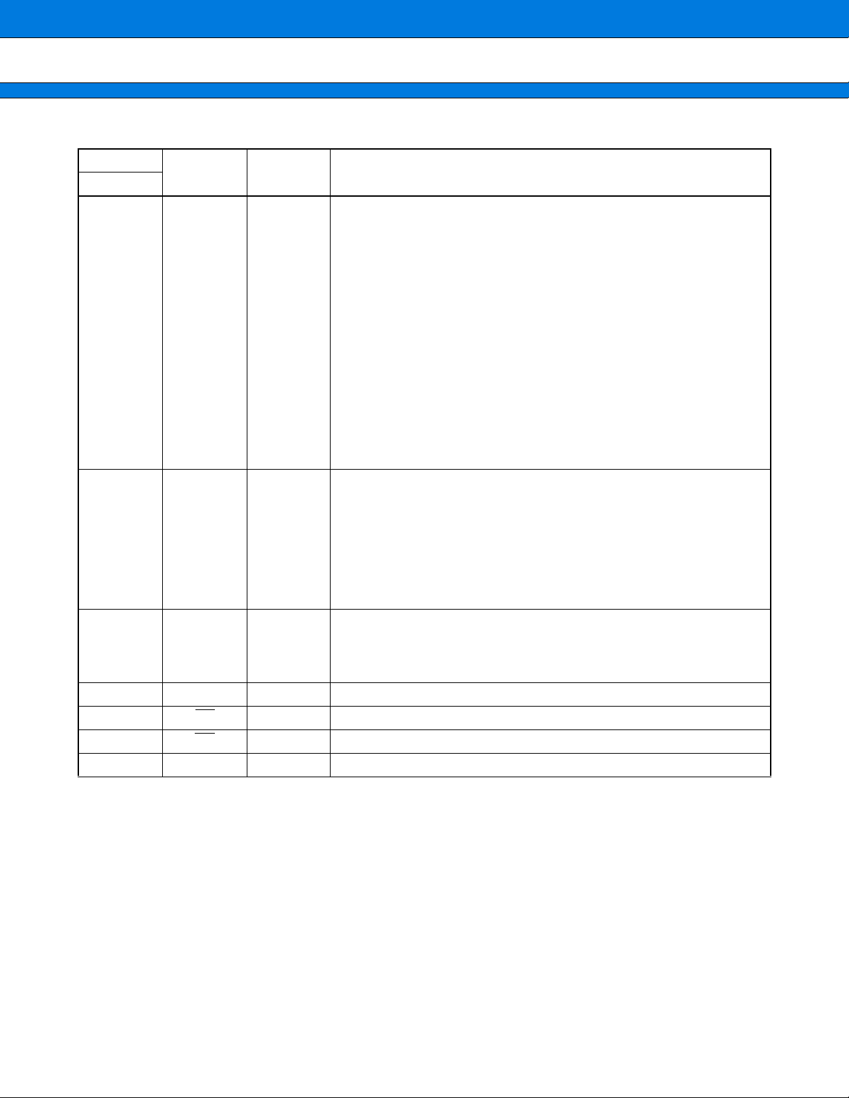
MB89490 Series
(Continued)
Parameter
UART/SIO
SIO
2C*2
I
Part number
Synchronous/asynchronous data transfer capability
(Max baud rate : 97.656 Kbps at 12.5 MHz)
(7-bit and 8-bit with parity bit; 8-bit and 9-bit without parity bit)
8-bit serial I/O with LSB first/MSB first selectability
1 clock selectable from 4 operation clock (1 external shift clock and 3 internal shift clock :
0.64 µs, 2.56 µs, 10.24 µs at 12.5 MHz)
1 channel
(Use a 2-wire protocol to communicate with other device)
MB89498 MB89F499 MB89PV490
Remote receiver
circuit
Standby mode Sleep mode, stop mode, watch mode and sub-clock mode
Process CMOS
Operating voltage 2.2 V to 3.6 V 2.7 V to 3.6 V 2.7 V to 3.6 V
*1 : Use MBM27C512 as the external ROM.
2
*2 : I
C is complied to Philips I2C specification.
Selectable maximum noise width removal
Reversible input polarity
4
PACKAGE AND CORRESPONDING PRODUCTS
■
MB89490 Series
Part number
Parameter
FPT-100P-M06 O O ×
FPT-100P-M05 O O ×
MQP-100C-P01 ××O
O : Availabe
× : Not available
DIFFERENCES AMONG PRODUCTS
■
MB89498 MB89F499 MB89PV490
1. Memory Size
Before e v aluating using the pigg y-back product, v erify its diff erences from the product that will be actually used.
Take particular care on the following point : The stack area is set at the upper limit of the RAM.
2. Current Consumption
• For the MB89PV490, add the current consumed by the EPROM mounted in the piggy-back socket.
• When operating at low speed, the current consumed by the FLASH product is greater than that for the mask
ROM product. However, the current consumption is roughly the same in sleep and stop mode.
• For more information, see “■ ELECTRICAL CHARACTERISTICS.”
3. Oscillation Stabilization Wait Time after Power-on Reset
• For MB89PV490 and MB89F499, the pow er-on stabilization wait time cannot be selected after power-on reset.
• For MB89498, the power-on stabilization wait time can be selected after power-on reset.
• For more information, please refer to “■ MASK OPTIONS”.
5
MB89490 Series
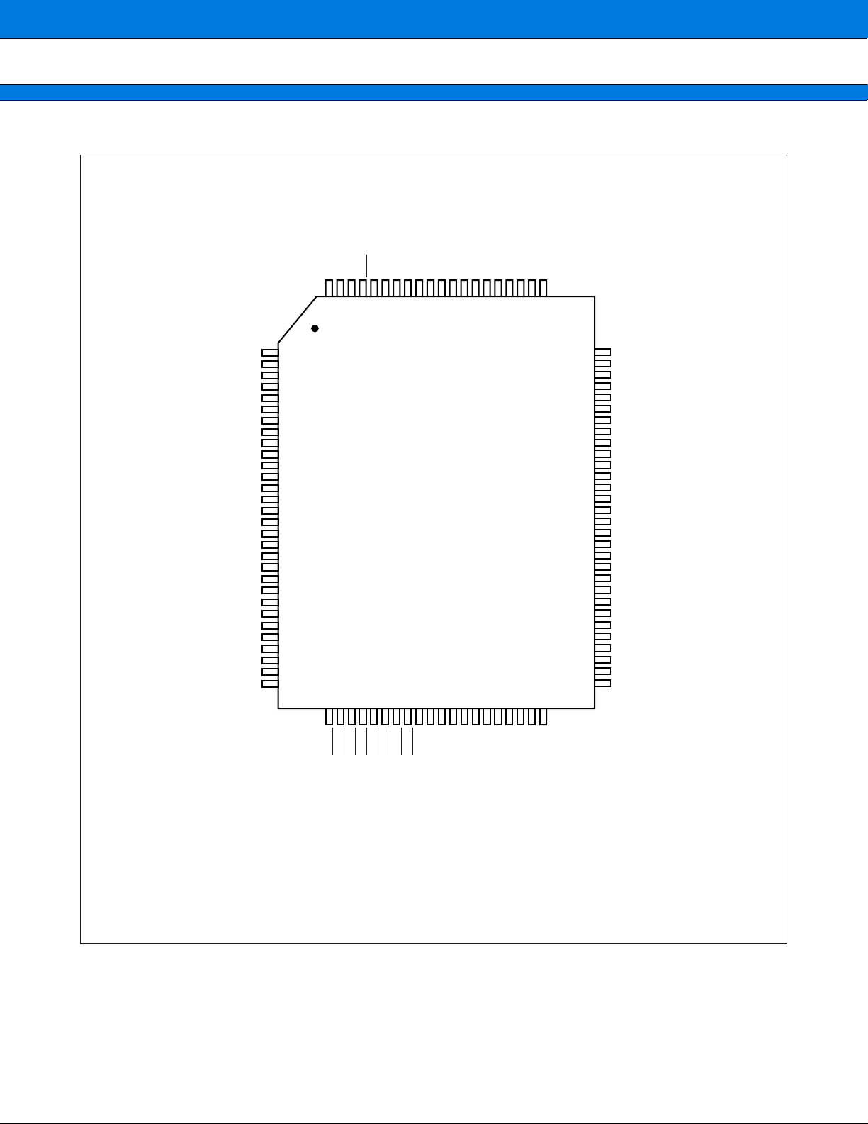
PIN ASSIGNMENTS
■
VCC
P23
CC
1
2
3
4
5
6
7
8
9
10
11
12
13
14
15
16
17
18
19
20
21
22
23
24
25
26
27
28
29
30
*P00
*P01
*P02
*P03
*P04
*P05
*P06
*P07
P10/INT00
P11/INT01
P12/INT02
P13/INT03
P14/INT04
P15/INT05
P16/INT06
P17/INT07
P20/TO0
P21/RMC
P22EC0
P24/TO1
P25/EC1
P26/PWM0
P27/PWM1
P50/SI0
P51/SO0
P52/SCK0
AVR
AV
(TOP VIEW)
VSSX0X1
MOD0
RST
P84
P83
P82/SCK1
P81/SO1
P80/SI1
P77/SEG31
P76/SEG30
P75/SEG29
P74/SEG28
P73/SEG27
P72/SEG26
P71/SEG25
P70/SEG24
P67/SEG23
99989796959493929190898887868584838281
100
31323334353637383940414243444546474849
P66/SEG22
80
79
78
77
76
75
74
73
72
71
70
69
68
67
66
65
64
63
62
61
60
59
58
57
56
55
54
53
52
51
50
P65/SEG21
P64/SEG20
P63/SEG19
P62/SEG18
P61/SEG17
P60/SEG16
SEG15
SEG14
SEG13
SEG12
SEG11
SEG10
SEG9
SEG8
SEG7
SEG6
SEG5
SEG4
SEG3
SEG2
SEG1
SEG0
P54/COM3
P53/COM2
COM1
COM0
V1
V2
V3
V
CC
* : High current pins
6
AVSS
P30/AN0/INT10
P31/AN1/INT11
P32/AN2/INT12
P33/AN3/INT13
P34/AN4/INT14
(FPT-100P-M06)
*P40
*P41
*P42
*P43
P35/AN5/INT15
P36/AN6/INT16
P37/AN7/INT17
*P44
*P45
X1A
X0A
*P46/SCL
*P47/SDA
SS
V
(Continued)
*P01
*P00
VCC
VSSX0X1
(TOP VIEW)
MOD0
RST
P84
P83
P82/SCK1
P81/SO1
P80/SI1
P77/SEG31
P76/SEG30
P75/SEG29
P74/SEG28
P73/SEG27
P72/SEG26
P71/SEG25
P70/SEG24
MB89490 Series
P67/SEG23
P66/SEG22
P65/SEG21
P64/SEG20
*P02
*P03
*P04
*P05
*P06
*P07
P10/INT00
P11/INT01
P12/INT02
P13/INT03
P14/INT04
P15/INT05
P16/INT06
P17/INT07
P20/TO0
P21/RMC
P22/EC0
P23
P24/TO1
P25/EC1
P26/PWM0
P27/PWM1
P50/SI0
P51/SO0
P52/SCK0
1
2
3
4
5
6
7
8
9
10
11
12
13
14
15
16
17
18
19
20
21
22
23
24
25
9998979695949392919089888786858483828180797877
100
26272829303132333435363738394041424344454647484950
X1A
AVR
AVSS
AVCC
*P40
*P41
*P42
*P43
*P44
*P45
X0A
*P46/SCL
*P47/SDA
SS
V
VCC
V3
76
V2
75
74
73
72
71
70
69
68
67
66
65
64
63
62
61
60
59
58
57
56
55
54
53
52
51
P63/SEG19
P62/SEG18
P61/SEG17
P60/SEG16
SEG15
SEG14
SEG13
SEG12
SEG11
SEG10
SEG9
SEG8
SEG7
SEG6
SEG5
SEG4
SEG3
SEG2
SEG1
SEG0
P54/COM3
P53/COM2
COM1
COM0
V1
* : High current pins
P30/AN0/INT10
P31/AN1/INT11
P32/AN2/INT12
P33/AN3/INT13
P34/AN4/INT14
P35/AN5/INT15
P36/AN6/INT16
(FPT-100P-M05)
P37/AN7/INT17
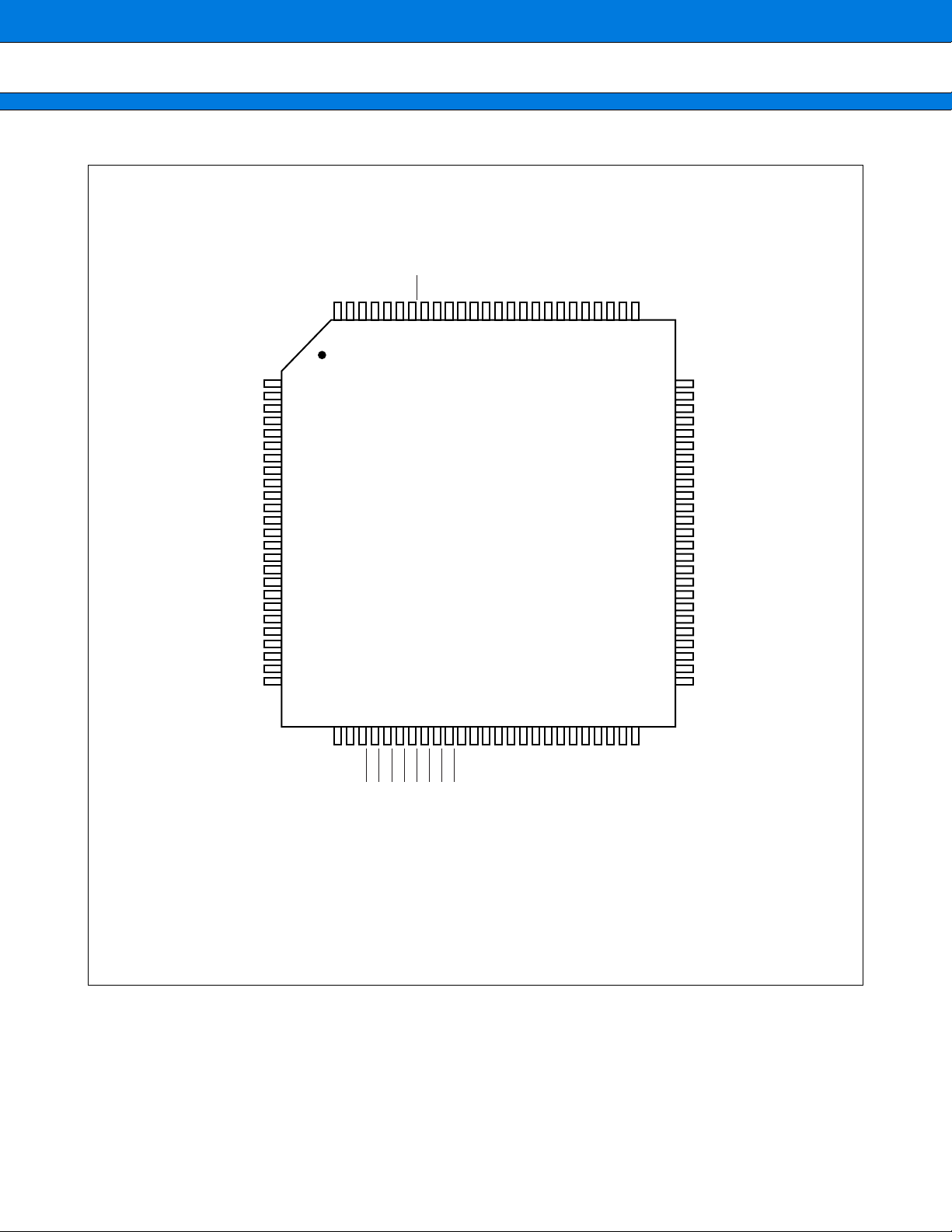
(Continued)
7
MB89490 Series
(Continued)
VCC
P23
CC
1
2
3
4
5
6
7
8
9
10
11
12
13
14
15
16
17
18
19
20
21
22
23
24
25
26
27
28
29
30
*P00
*P01
*P02
*P03
*P04
*P05
*P06
*P07
P10/INT00
P11/INT01
P12/INT02
P13/INT03
P14/INT04
P15/INT05
P16/INT06
P17/INT07
P20/TO0
P21/RMC
P22EC0
P24/TO1
P25/EC1
P26/PWM0
P27/PWM1
P50/SI0
P51/SO0
P52/SCK0
AVR
AV
(TOP VIEW)
VSSX0X1
MOD0
RST
P84
P83
P82/SCK1
P81/SO1
P80/SI1
P77/SEG31
P76/SEG30
P75/SEG29
P74/SEG28
P73/SEG27
P72/SEG26
P71/SEG25
P70/SEG24
P67/SEG23
99989796959493929190898887868584838281
100
120
119
118
117
116
115
114
121
122
123
124
125
126
127
128
129
130
131
31323334353637383940414243444546474849
132
101
102
113
112
111
110
109
108
107
106
105
103
104
P66/SEG22
80
79
78
77
76
75
74
73
72
71
70
69
68
67
66
65
64
63
62
61
60
59
58
57
56
55
54
53
52
51
50
P65/SEG21
P64/SEG20
P63/SEG19
P62/SEG18
P61/SEG17
P60/SEG16
SEG15
SEG14
SEG13
SEG12
SEG11
SEG10
SEG9
SEG8
SEG7
SEG6
SEG5
SEG4
SEG3
SEG2
SEG1
SEG0
P54/COM3
P53/COM2
COM1
COM0
V1
V2
V3
V
CC
SS
V
X1A
X0A
*P46/SCL
*P47/SDA
* : High current pins
AVSS
P30/AN0/INT10
P31/AN1/INT11
P32/AN2/INT12
P33/AN3/INT13
P34/AN4/INT14
(MQP-100C-P01)
*P40
*P41
*P42
P35/AN5/INT15
P36/AN6/INT16
P37/AN7/INT17
*P43
*P44
*P45
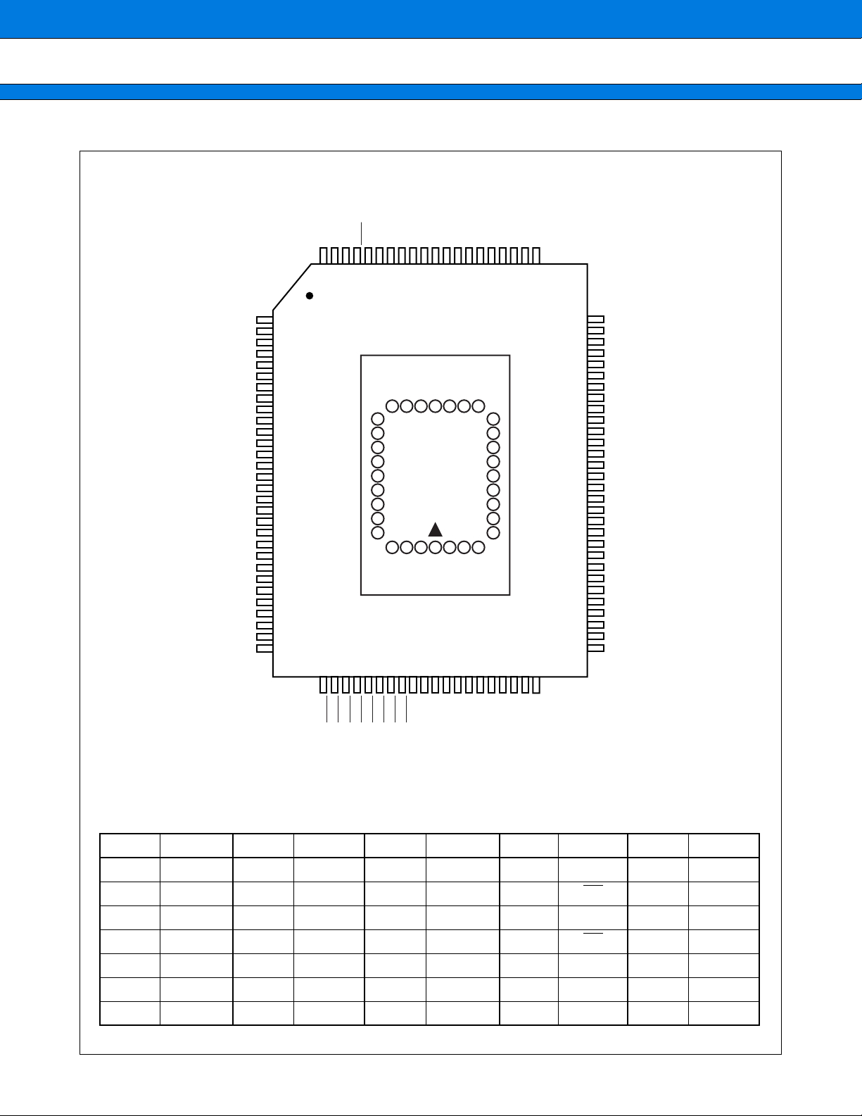
Pin assignment on package top (MB89PV490 only)
Pin no. Pin name Pin no. Pin name Pin no. Pin name Pin no. Pin name Pin no. Pin name
101 N.C. 108 A3 115 O3 122 O8 129 A8
102 A15 109 A2 116 V
SS 123 CE 130 A13
103 A12 110 A1 117 N.C. 124 A10 131 A14
104 A7 111 A0 118 O4 125 OE
132 VCC
105 A6 112 N.C. 119 O5 126 N.C.
106 A5 113 O1 120 O6 127 A11
107 A4 114 O2 121 O7 128 A9
N.C. : As connected internally, do not use.
8
PIN DESCRIPTION
■
MB89490 Series
Pin number
MQFP*
QFP*
1
/
2
LQFP*
3
Pin name
99 96 X0
98 95 X1
49 46 X0A
48 45 X1A
97 94 MOD0 B
I/O circuit
type
A
A
Function
Connection pins for a crystal or other oscillator circuit.
An external clock can be connected to X0. In this case, leave
X1 open.
Connection pins for a crystal or other oscillator circuit.
An external clock can be connected to X0A. In this case, leave
X1A open.
Input pin for setting the memory access mode.
Connect directly to V
SS.
95, 94 92, 91 P84, P83 J General-purpose CMOS input port.
Reset I/O pin. The pin is an N-ch open-drain type with pull-up
96 93 RST
C
resistor and hysteresis input. The pin outputs an “L” level when
an internal reset request is present. Inputting an “L” level initializes internal circuits.
2 to 9 99 to 6 P00 to P07 D General-purpose CMOS I/O port.
P10/INT00
10 to 17 7 to 14
to
P17/INT07
18 15 P20/TO0 F
E
General-purpose CMOS I/O port.
The pin is shared with external interrupt 0 input.
General-purpose CMOS I/O port.
The pin is shared with 8/16-bit timer/counter 00 and 01 output.
19 16 P21/RMC E
20 17 P22/EC0 E
General-purpose CMOS I/O port.
The pin is shared with remote receiver input.
General-purpose CMOS I/O port.
The pin is shared with 8/16-bit timer/counter 00 and 01 input.
21 18 P23 F General-purpose CMOS I/O port.
22 19 P24/TO1 F
23 20 P25/EC1 E
24 21 P26/PWM0 F
25 22 P27/PWM1 F
P30/AN0/INT10
32 to 39 29 to 36
to
P37/AN7/INT17
G
General-purpose CMOS I/O port.
The pin is shared with 8/16-bit timer/counter 10 and 11 output.
General-purpose CMOS I/O port.
The pin is shared with 8/16-bit timer/counter 10 and 11 input.
General-purpose CMOS I/O port.
The pin is shared with PWM0 output.
General-purpose CMOS I/O port.
The pin is shared with PWM1 output.
General-purpose CMOS I/O port.
The pin is shared with external interrupt 1 input and A/D
converter input.
40 to 45 37 to 42 P40 to P45 H General-purpose N-ch open-drain I/O port.
46 43 P46/SCL H
General-purpose N-ch open-drain I/O port.
The pin is shared with I
2
C clock I/O.
(Continued)
9
MB89490 Series
(Continued)
Pin number
1
2
/
LQFP*
MQFP*
QFP*
47 44 P47/SDA H
Pin name
3
I/O circuit
type
Function
General-purpose N-ch open-drain I/O port.
The pin is shared with I
2
C data I/O.
26 23 P50/SI0 E
27 24 P51/SO0 F
28 25 P52/SCK0 E
57 54 P53/COM2 F/I
58 55 P54/COM3 F/I
P60/SEG16
75 to 82 72 to 79
to
P67/SEG23
P70/SEG24
83 to 90 80 to 87
to
P77/SEG31
91 88 P80/SI1 E
92 89 P81/SO1 F
93 90 P82/SCK1 E
F/I
F/I
General-purpose CMOS I/O port.
The pin is shared with SIO data input.
General-purpose CMOS I/O port.
The pin is shared with SIO data output.
General-purpose CMOS I/O port.
The pin is shared with SIO clock I/O.
General-purpose CMOS I/O port.
The pin is shared with the LCD common output.
General-purpose CMOS I/O port.
The pin is shared with the LCD common output.
General-purpose CMOS I/O port.
The pin is shared with LCD segment output.
General-purpose CMOS I/O port.
The pin is shared with LCD segment output.
General-purpose CMOS I/O port.
The pin is shared with UART/SIO data input.
General-purpose CMOS I/O port.
The pin is shared with UART/SIO data output.
General-purpose CMOS I/O port.
The pin is shared with UART/SIO clock I/O.
59 to 74 56 to 71
55, 56 52, 53
54, 53, 5251, 50,
49
1, 51 98, 48 V
50, 100 47, 97 V
30 27 AV
29 26 AVR A/D converter reference voltage input pin.
31 28 AV
*1 : MQP-100C-P01
*2 : FPT-100P-M06
*3 : FPT-100P-M05
10
SEG0 to
SEG15
COM0,
COM1
I LCD segment output-only pin.
I LCD common output-only pin.
V1 to V3 LCD driving power supply pin.
CC Power supply pin.
SS Power supply pin (GND) .
CC A/D converter power supply pin.
SS
A/D converter power supply pin.
Use at the same voltage level as VSS.
MB89490 Series
•
External EPROM Socket (MB89PV490 only)
Pin number
MQFP*
102
131
130
103
127
124
128
129
104
105
106
107
108
109
110
111
122
121
120
119
118
115
114
113
101
112
117
126
Pin name I/O Function
A15
A14
A13
A12
A11
A10
A9
A8
A7
A6
A5
A4
A3
A2
A1
A0
O8
O7
O6
O5
O4
O3
O2
O1
N.C. Internally connected pins. Always leave open.
O Address output pins.
I Data input pins.
116 V
123 CE
125 OE O Output enable pin for the EPROM. Always outputs “L”.
132 V
* : MQP-100C-P01
SS O Power supply pin (GND) .
O Chip enable pin for the EPROM. Outputs “H” in standby mode.
CC O Power supply pin for the EPROM.
11
MB89490 Series
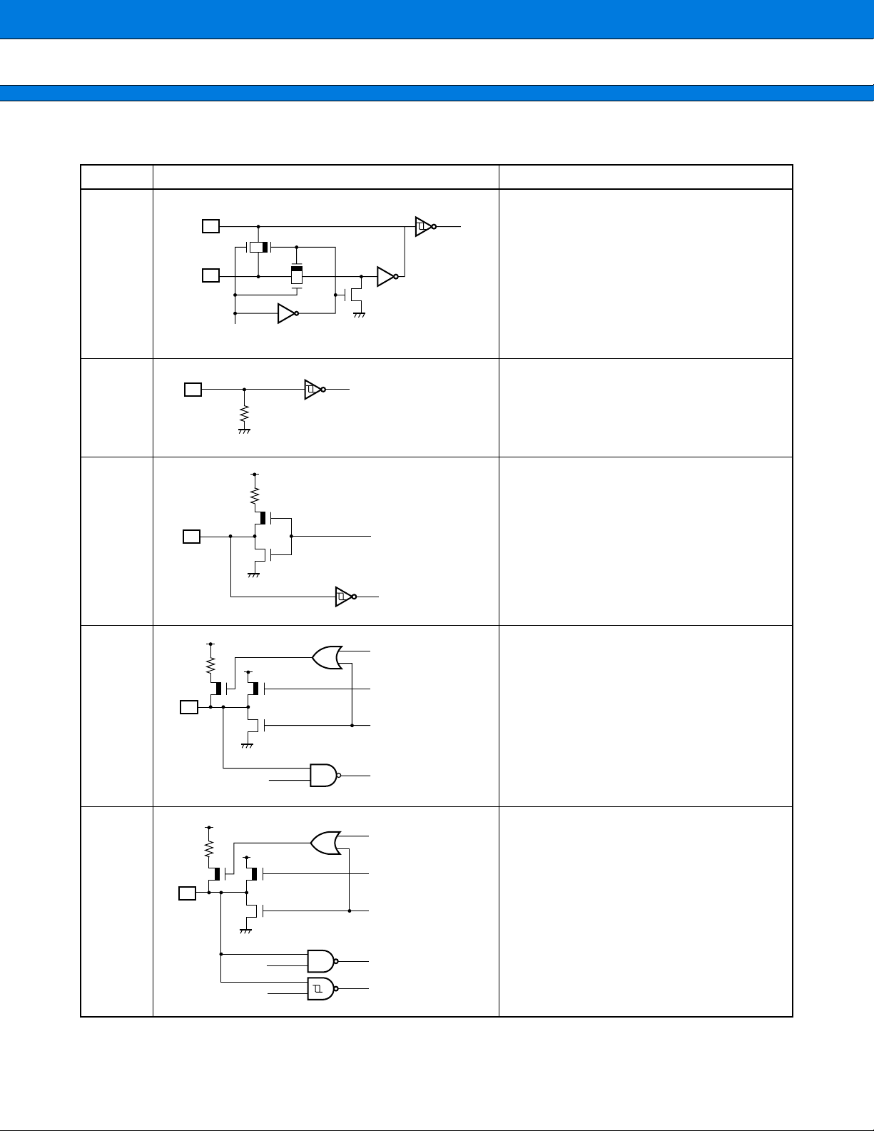
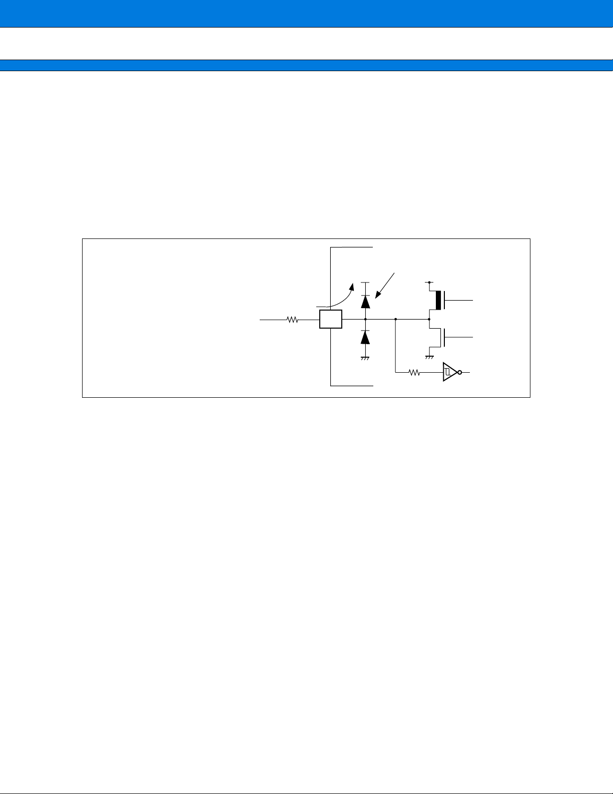
I/O CIRCUIT TYPE
■
Type Circuit Remarks
X1 (X1A)
N-ch
P-ch
X0 (X0A)
P-ch
A
N-ch
Stop mode control signal
B
R
R
P-ch
N-ch
• Main/Sub-clock circuit
• Hysteresis input
(CMOS input in MB89F499)
• The pull-down resistor
(not available in MB89F499)
Approx. 50 kΩ
• The pull-up resistor (P-channel)
Approx. 50 kΩ
• Hysteresis input
C
N-ch
R
P-ch
P-ch
pull-up
resistor register
D
N-ch
port
• CMOS output
•I
OH = − 4 mA, IOL = 12 mA
• CMOS input
• Selectable pull-up resistor
Approx. 50 kΩ
• CMOS output
R
P-ch
pull-up
resistor register
P-ch
•I
OH = − 2 mA, IOL = 4 mA
• CMOS port input
• Hysteresis resource input
• Selectable pull-up resistor
E
N-ch
Approx. 50 kΩ
12
port
resource
(Continued)
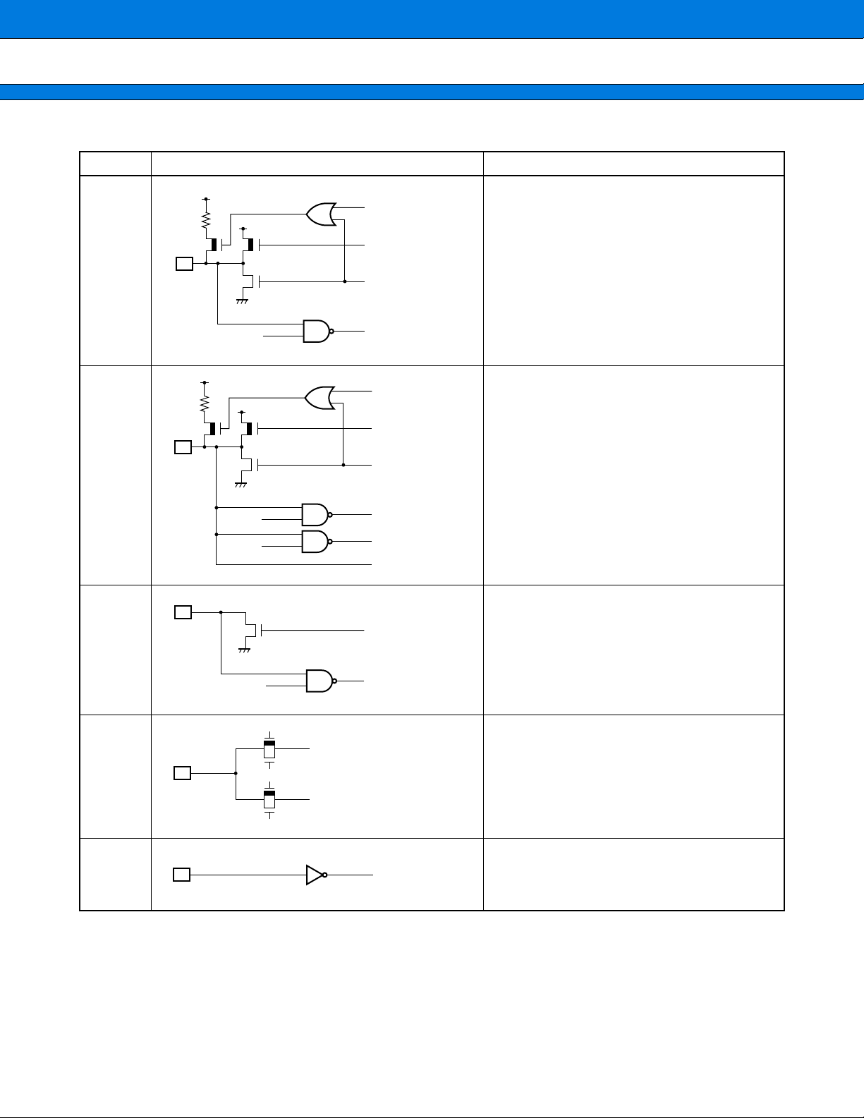
MB89490 Series
(Continued)
Type Circuit Remarks
• CMOS output
pull-up
resistor register
P-ch
R
P-ch
F
N-ch
port
•I
OH = − 2 mA, IOL = 4 mA
• CMOS input
• Selectable pull-up resistor
Approx. 50 kΩ
• CMOS output
P-ch
R
P-ch
pull-up
resistor register
OH = − 2 mA, IOL = 4 mA
•I
• CMOS port input
•V
IH = 0.85 VCC, VIL = 0.5 VCC resource input
• Analog input
G
N-ch
• Selectable pull-up resistor
Approx. 50 kΩ
port
resource
analog
• N-ch open-drain output
•I
OL = 15 mA
H
N-ch
port/resource
• CMOS port input
• CMOS resource input
•5 V tolerance
• LCD segment output
P-ch
N-ch
I
P-ch
N-ch
• CMOS input
J
13

MB89490 Series
HANDLING DEVICES
■
1. Preventing Latch-up
Latch-up may occur on CMOS IC if voltage higher than VCC or lo wer than VSS is applied to input and output pins
other than medium- to high-voltage pins or if higher than the voltage which shows on “1. Absolute Maximum
Ratings” in “■ ELECTRICAL CHARACTERISTICS” is applied between V
When latch-up occurs, power supply current increases rapidly and might thermally damage elements. When
using, take great care not to exceed the maximum ratings.
Also, take care to prevent the analog power supply (AV
power supply (V
CC) when the analog system power supply is turned on and off.
CC and AVR) and analog input from exceeding the digital
2. Treatment of Unused Input Pins
Leaving unused input pins open could cause malfunctions. The y should be connected to a pull-up or pull-do wn
resistor.
3. Treatment of Power Supply Pins on Microcontrollers with A/D
Connect to be AVCC = VCC and AVSS = AVR = VSS even if the A/D is not in use.
CC and VSS.
4. Treatment of N.C. Pins
Be sure to leave (internally connected) N.C. pins open.
5. Power Supply Voltage Stabilization
Although VCC power supply voltage is assured to oper ate within the rated range, a rapid fluctuation of the v oltage
could cause malfunctions, even if it occurs within the r ated range. As stabilization guidelines, it is recommended
to control voltage fluctuation so that V
value at the commercial frequency (50 Hz to 60 Hz) and the transient fluctuation rate will be less than 0.1 V/ms
at the time of a momentary fluctuation such as when power is switched.
CC ripple fluctuations (P-P value) will be less than 10% of the standard VCC
6. Precautions when Using an External Clock
Even when an external clock is used, oscillation stabilization time is required for power-on reset and wake-up
from stop mode.
7. Treatment of Unused dedicated LCD pins
When dedicated LCD pins are not in use, keep them open.
14

MB89490 Series
PROGRAMMING AND ERASING FLASH MEMORY ON THE MB89F499
■
1. Flash Memory
The flash memory is located between 1000H and FFFFH in the CPU memor y map and incorporates a flash
memory interface circuit that allows read access and program access from the CPU to be perf ormed in the same
way as mask ROM. Programming and erasing flash memory is also performed via the flash memory interface
circuit by executing instructions in the CPU. This enables the flash memory to be updated in place under the
control of the internal CPU, providing an efficient method of updating program and data.
2. Flash Memory Features
• 60K bytes × 8-bit configuration (16 K + 8 K + 8 K + 28 K sectors)
• Automatic algorithm (Embedded algorithm* : Equivalent to MBM29LV200)
• Includes an erase pause and erase restart function
• Data polling and toggle bit for detection of program/erase completion
• Detection of program/erase completion via CPU interrupt
• Compatible with JEDEC-standard commands
• Sector Protection (sectors can be combined in any combination)
• No. of program/erase cycles : 10,000 (Min)
* : Embedded Algorithm is a trademark of Advanced Micro Devices.
3. Procedure for Programming and Erasing Flash Memory
Programming and reading flash memory cannot be performed at the same time. Accordingly, to program or
erase data to the flash memory, the program must first be copied from flash memory to RAM so that programming
can be performed without program access from flash memory.
4. Flash Memory Register
• Flash memory control status register (FMCS)
Address
007A
H
Bit 7 Bit 6 Bit 5 Bit 4 Bit 3 Bit 2 Bit 1 Bit 0
INTE RDYINT WE RDY Reserved Reserved
R/W R/W R/W R R/W R/W R/W
Reserved
Initial value
000X00-0
B
15

MB89490 Series
5. Sector Configuration
The table below shows the sector configuration of flash memory and lists the addresses of each sector during
CPU access and a flash memory programming.
• Sector configuration of flash memory
Flash Memory CPU Address Programmer Address*
16 K bytes FFFF
8 K bytes BFFFH to A000H 1BFFFH to 1A000H
8 K bytes 9FFFH to 8000H 19FFFH to 18000H
28 K bytes 7FFFH to 1000H 17FFFH to 11000H
* : The programmer address is the address to be used instead of the CPU address when programming data from
a parallel flash memory programmer. Use the prog rammer address on programming or erasing using a gener alpurpose programmer.
H to C000H 1FFFFH to 1C000H
6. ROM Programmer Adaptor and Recommended ROM Programmers
Package
FPT-100P-M06 FLASH-100QF-32DP-8LF2
FPT-100P-M05 FLASH-100SQF-32DP-8LF
* : For the programmer and the version of the programmer,contact the Flash Support Group, Inc.
Inquirues : Sunhayato Corp. : TEL : 81-(3)-3984-7791
Flash Support Group, Inc. : FAX : 81-(53)-428-8377
Applicable adapter model Recommended writer
Sunhayato Corp. Ando Electric Co. Ltd.
AF9708 (ver 1.60 or later) *
AF9709 (ver 1.60 or later) *
FAX : 81-(3)-3971-0535
E-mail : adapter@sunhayato.co.jp
E-mail : support@j-fsg.co.jp
16
MB89490 Series
PROGRAMMING TO THE EPROM WITH PIGGY-BACK/EVALUATION DEVICE
■
1. EPROM for Use
MBM27C512-20TV
2. Programming Socket Adapter
To program to the PROM using an EPROM programmer, use the socket adapter (manufacturer : Sunhayato
Corp.) .
Package Adapter socket part number
LCC-32 (Rectangle) ROM-32LC-28DP-YG
Inquiry : Sunhayato Corp. : TEL : 81-3-3984-7791
FAX : 81-3-3971-0535
E-mail : adapter@sunhayato.co.jp
3. Memory Space
Memory space corresponding to EPROM writer is shown in the diagram below.
Address Corresponding addresses
0000H
0080H
0880H
1000H 1000H
FFFFH FFFFH
Normal operating mode
I/O
RAM
Not available
PROM
60 KB
4. Programming to the EPROM
(1) Set the EPROM programmer to the MBM27C512.
(2) Load program data into the EPROM programmer at 1000
(3) Program to 1000
H to FFFFH with the EPROM programmer.
on the EPROM programmer
EPROM
60 KB
H to FFFFH.
ICE PROBE POD ADAPTOR OF PIGGY-BACK/EVA CHIP
■
The following conversion adapter is required to achieve the same pin layout as the FPT-100P-M05.
Adaptor part number: 100QF-100SQF-8L
Inquiry : Sunhayato Corp. : TEL : 81-3-3984-7791
FAX : 81-3-3971-0535
E-mail : adapter@sunhayato.co.jp
17
MB89490 Series
BLOCK DIAGRAM
■
X0A
X1A
RST
P23
P26/PWM0
P27/PWM1
P21/RMC
P22/EC0
P20/TO0
P25/EC1
P24/TO1
P17/INT07 to
P10/INT00
P07 to P00
ROM 48 K bytes/FLASH 60 K bytes
X0 Main clock
X1
8
8
Port0*
RAM (2 K bytes)
oscillator circuit
Clock controller
Sub-clock
oscillator circuit
Reset circuit
(Watchdog timer)
Watch prescaler
CMOS I/O port
8-bit PWM timer 0
8-bit PWM timer 1
Port2
Remote receiver circuit
timer/counter 00, 01
timer/counter 10, 11
8
External interrupt 0
CMOS I/O port
Port1
CMOS I/O port
2
F
MC-8L
CPU
8/16-bit
8/16-bit
(edge)
21-bit timebase
timer
10-bit
A/D converter
CMOS I/O port
External interrupt 1
(level)
I
N-ch open-drain I/O port
CMOS I/O port
Internal data bus
UART/SIO
SIO
CMOS I/O port
LCD controller/driver
32 × 4-bit display
RAM (16 bytes)
CC
AV
AVSS
AVR
8
P37/AN7/INT17
8
to
P30/AN0/INT10
Port3
8
Port4*
6
Port8
Port5
2
16
2
3
8
8
Port6, 7
P47/SDA
P46/SCL
P45 to P40
P84
P83
P82/SCK1
P81/SO1
P80/SI1
P52/SCK0
P51/SO0
P50/SI0
P54/COM3,
P53/COM2
SEG0
to SEG15
COM0,
COM1
V1 to V3
P67/SEG23
to P60/SEG16
P77/SEG31
to P70/SEG24
2
C
2
16
* : High current I/O port.
18
Other pins
V
CC × 2, VSS × 2, MOD0
CMOS I/O port

MB89490 Series
CPU CORE
■
1. Memory Space
The microcontrollers of the MB89490 series offer a memory space of 64K bytes for storing all of I/O, data, and
program areas. The I/O area is located the lowest address. The data area is provided immediately above the
I/O area. The data area can be divided into register, stack, and direct areas according to the application. The
program area is located at exactly the opposite end, that is, near the highest address. Provide the tables of
interrupt/reset vectors and vector call instructions toward the highest address within the program area. The
memory space of the MB89490 series is structured as illustrated below.
Memory Space
MB89498
0000
H
I/O
0080H
0100H
0200H
0880H
4000H
FFC0H
FFFFH
Vector table (reset, interrupt, vector call instruction)
RAM
Generalpurpose
registers
Vacant
ROM
0000
0080H
0100H
0200H
0880H
1000H
FFC0H
FFFFH
MB89F499
H
Generalpurpose
registers
MB89PV490
0000
H
I/O
0080H
RAM
Vacant Vacant
FLASH
(60 K)
0100H
0200H
0880H
1000H
FFC0H
FFFFH
I/O
RAM
Generalpurpose
registers
External
ROM
(60 K)
19
MB89490 Series
2. Registers
The F2MC-8L family has 2 types of registers; dedicated registers in the CPU and general-purpose registers in
the memory. The following registers are provided :
Program counter (PC) : A 16-bit register for indicating instruction storage positions.
Accumulator (A) : A 16-bit temporary register for storing arithmetic operations, etc. When the
instruction is an 8-bit data processing instruction, the lower byte is used.
Temporary accumulator (T) : A 16-bit register for performing arithmetic operations with the accumulator.
When the instruction is an 8-bit data processing instruction, the lower byte is used.
Index register (IX) : A 16-bit register for index modification.
Extra pointer (EP) : A 16-bit pointer for indicating a memory address.
Stack pointer (SP) : A 16-bit register for indicating a stack area.
Program status (PS) : A 16-bit register for storing a register pointer and condition code.
16-bit
PC
A
T
IX
EP
SP
PS
: Program counter
: Accumulator
: Temporary accumulator
: Index register
: Extra pointer
: Stack pointer
: Program status
Initial value
FFFD
H
Undefined
Undefined
Undefined
Undefined
Undefined
I-flag = 0, IL1, 0 = 11
Other bits are undefined.
The PS can further be divided into higher 8-bit for use as a register bank pointer (RP) and the lower 8-bit for
use as a condition code register (CCR) . (See the diagram below.)
Structure of the Program Status Register
109876 321015 14 13 12 11
Va-
Va-
RPPS
Va-
cancy
cancy
H I IL1, 0 N Z VC
cancy
54
20
RP CCR
MB89490 Series
The RP indicates the address of the register bank currently in use. The relationship between the pointer contents
and the actual address is based on the conversion rule illustrated below.
Conversion rule for Actual Addresses of the General-purpose Register Area
RP
“0” “0” “0” “0” “0” “0” “0” “1” R4 R3 R2 R1 R0 b2 b1 b0
Generated addresses
The CCR consists of bits indicating the results of arithmetic operations and the contents of transfer data and
bits for controlling the CPU operations at the time of an interrupt.
H-flag : Set to “1” when a carry or a borrow from bit 3 to bit 4 occurs as a result of an arithmetic operation. Clear
to “0” otherwise. This flag is for decimal adjustment instructions.
I-flag : Interrupt is allowed when this flag is set to “1”. Interrupt is prohibited when the flag is set to “0”. Clear to
“0” at reset.
IL1, 0 : Indicates the level of the interrupt currently allowed. Processes an interrupt only if its request is higher
than the value indicated by this bit.
IL1 IL0 Interrupt level High-low
00
01
A15 A14 A13 A12 A11 A10 A9 A8 A7 A6 A5 A4 A3 A2 A1 A0
1
Lower OP codes
High
10 2
11 3
N-flag : Set to “1” if the MSB is set to “1” as the result of an arithmetic operation. Clear to “0” otherwise.
Z-flag : Set to “1” when an arithmetic operation results in “0”. Clear to “0” otherwise.
V-flag : Set to “1” if the complement on 2 overflows as a result of an arithmetic operation. Clear to “0” if the
overflow does not occur.
C-flag : Set to “1” when a carry or a borrow from bit 7 occurs as a result of an arithmetic operation. Clear to “0”
otherwise. Set to the shift-out value in the case of a shift instruction.
Low
21

MB89490 Series
The following general-purpose registers are provided :
General-purpose registers : An 8-bit register for storing data
The general-purpose registers are 8-bit and located in the register banks of the memory.
1 bank contains 8 registers. Up to a total of 32 banks can be used on the MB89490 series. The bank currently
in use is indicated by the register bank pointer (RP) .
Register Bank Configuration
This address = 0100H + 8 × (RP)
R 0
R 1
R 2
R 3
R 4
R 5
R 6
R 7
32 banks
Memory area
22

MB89490 Series
I/O MAP
■
Address Register name Register description Read/Write Initial value
00
H PDR0 Port 0 data register R/W XXXXXXXXB
01H DDR0 Port 0 direction register W* 00000000B
02H PDR1 Port 1 data register R/W XXXXXXXXB
03H DDR1 Port 1 direction register W* 00000000B
04H PDR2 Port 2 data register R/W 00000000B
05H (Reserved)
06
H DDR2 Port 2 direction register R/W 00000000B
07H SYCC System clock control register R/W X-1MM100B
08H STBC Standby control register R/W 00010XXXB
09H WDTC Watchdog timer control register W* 0---XXXXB
0AH TBTC Timebase timer control register R/W 00---000B
0BH WPCR Watch prescaler control register R/W 00--0000B
0CH PDR3 Port 3 data register R/W XXXXXXXXB
0DH DDR3 Port 3 direction register R/W 11111111B
0EH RSFR Reset flag register R XXXX----B
0FH PDR4 Port 4 data register R/W 11111111B
10H PDR5 Port 5 data register R/W ---XXXXXB
11H DDR5 Port 5 direction register R/W ---00000B
12H PDR6 Port 6 data register R/W XXXXXXXXB
13H DDR6 Port 6 direction register R/W 00000000B
14H PDR7 Port 7 data register R/W XXXXXXXXB
15H DDR7 Port 7 direction register R/W 00000000B
16H PDR8 Port 8 data register R/W ---XXXXXB
17H DDR8 Port 8 direction register R/W ---00000B
18H EIC0 External interrupt 0 control register 0 R/W 00000000B
19H EIC1 External interrupt 0 control register 1 R/W 00000000B
1AH EIC2 External interrupt 0 control register 2 R/W 00000000B
1BH EIC3 External interrupt 0 control register 3 R/W 00000000B
1CH EIE1 External interrupt 1 enable register R/W 00000000B
1DH EIF1 External interrupt 1 flag register R/W -------0B
1EH SMR Serial mode register R/W 00000000B
1FH SDR Serial data register R/W XXXXXXXXB
20H T01CR Timer 01 control register R/W 000000X0B
21H T00CR Timer 00 control register R/W 000000X0B
22H T01DR Timer 01 data register R/W XXXXXXXXB
(Continued)
23

MB89490 Series
Address Register name Register description Read/Write Initial value
23
H T00DR Timer 00 data register R/W XXXXXXXXB
24H T11CR Timer 11 control register R/W 000000X0B
25H T10CR Timer 10 control register R/W 000000X0B
26H T11DR Timer 11 data register R/W XXXXXXXXB
27H T10DR Timer 10 data register R/W XXXXXXXXB
28H ADER A/D input enable register R/W 11111111B
29H ADC0 A/D control register 0 R/W -00000X0B
2AH ADC1 A/D control register 1 R/W -0000001B
2BH ADDH A/D data register (Upper byte) R ------XXB
2CH ADDL A/D data register (Lower byte) R XXXXXXXXB
2DH CNTR0 PWM 0 timer control register R/W 0-000000B
2EH COMR0 PWM 0 timer compare register W* XXXXXXXXB
2FH SMC0 UART/SIO serial mode control register R/W 00000000B
30H SMC1 UART/SIO serial mode control register R/W 00000000B
31H SSD UART/SIO serial status/data register R/W 00001---B
32H SIDR/SODR UART/SIO serial data register R/W XXXXXXXXB
33H SRC UART/SIO serial rate control register R/W XXXXXXXXB
34H CNTR1 PWM 1 timer control register R/W 0-000000B
35H COMR1 PWM 1 timer compare register W* XXXXXXXXB
36H IBSR I2C bus status register R 00000000B
37H IBCR I2C bus control register R/W 00000000B
38H ICCR I2C clock control register R/W 000XXXXXB
39H IADR I2C address register R/W -XXXXXXXB
3AH IDAR I2C data register R/W XXXXXXXXB
3BH PLLCR Sub PLL control register R/W ----0000B
3CH to 3FH (Reserved)
40H RMN Remote control counter register R XXXXXXXXB
41H RMC Remote control control register R/W 00000000B
42H RMS Remote control status register R/W 0X000001B
43H RMD Remote control FIFO data register R X----XXXB
44H RMCD0 Remote control compare register 0 R/W 11111111B
45H RMCD1 Remote control compare register 1 R/W 11111111B
24
46H RMCD2 Remote control compare register 2 R/W 11111111B
47H RMCD3 Remote control compare register 3 R/W 11111111B
48H RMCD4 Remote control compare register 4 R/W 11111111B
(Continued)

MB89490 Series
(Continued)
Address Register name Register description Read/Write Initial value
49
H RMCD5 Remote control compare register 5 R/W 11111111B
4AH RMCI Remote interrupt register R/W 0000-000B
4BH to 5DH (Reserved)
5E
H LOCR LCD controller output control register R/W -0000000B
5FH LCR LCD controller control register R/W 00010000B
60H to 6FH VRAM LCD data RAM R/W XXXXXXXXB
70H PUCR0 Port 0 pull up resistor control register R/W 11111111B
71H PUCR1 Port 1 pull up resistor control register R/W 11111111B
72H PUCR2 Port 2 pull up resistor control register R/W 11111111B
73H PUCR3 Port 3 pull up resistor control register R/W 11111111B
74H PUCR5 Port 5 pull up resistor control register R/W ---11111B
75H PUCR6 Port 6 pull up resistor control register R/W 11111111B
76H PUCR7 Port 7 pull up resistor control register R/W 11111111B
77H PUCR8 Port 8 pull up resistor control register R/W -----111B
78H to 79H (Reserved)
7A
H FMCS Flash memory control status registger R/W 000X00-0B
7BH ILR1 Interrupt level setting register 1 W* 11111111B
7CH ILR2 Interrupt level setting register 2 W* 11111111B
7DH ILR3 Interrupt level setting register 3 W* 11111111B
7EH ILR4 Interrupt level setting register 4 W* 11111111B
7FH (Reserved)
* : Bit manipulation instruction cannot be used.
•
Read/write access symbols
R/W : Readable and writable
R : Read-only
W : Write-only
•
Initial value symbols
0 : The initial value of this bit is “0”.
1 : The initial value of this bit is “1”.
X : The initial value of this bit is undefined.
- : Unused bit.
M : The initial value of this bit is determined by mask option.
25

MB89490 Series
ELECTRICAL CHARACTERISTICS
■
1. Absolute Maximum Ratings
Parameter
Symbol
Rating
Unit Remarks
Min Max
Power supply voltage*
VCC
1
AVCC
VSS − 0.3 VSS + 4.0 V AVCC must be equal to VCC
AVR VSS − 0.3 VSS + 4.0 V
LCD power supply voltage V1 to V3 V
SS − 0.3 VCC V
VSS − 0.3 VCC + 0.3 V Except P40 to P47
Input voltage *
Output voltage*
Maximum clamp current I
1
1
VI
VO VSS − 0.3 VCC + 0.3 V
CLAMP − 2.0 + 2.0 mA *2
Total maximum clamp current Σ|I
CLAMP| 20 mA *2
V
SS − 0.3 VSS + 6.0 V
V
SS − 0.3 VSS + 5.5 V P40 to P47 in MB89F499
“L” level maximum output current IOL 15 mA
“L” level average output current I
“L” level total maximum output
current
“L” level total average output
current
OLAV 4mA
ΣI
OL 100 mA
ΣI
OLAV 40 mA
“H” level maximum output current IOH − 15 mA
P40 to P47 in MB89PV490 and
MB89498
Average value (operating current ×
operating rate)
Average value (operating current ×
operating rate)
“H” level average output current I
“H” level total maximum output
current
“H” level total average output
current
Power consumption P
Operating temperature T
OHAV − 4mA
ΣI
OH − 50 mA
ΣIOHAV − 20 mA
D 300 mW
A − 40 + 85 °C
Average value (operating current ×
operating rate)
Average value (operating current ×
operating rate)
Storage temperature Tstg − 55 + 150 °C
*1 : The parameter is based on AVSS = VSS = 0.0 V.
*2 : • Applicable to pins : P00 to P07, P10 to P17, P20 to P27, P30 to P37, P50 to P52, P80 to P82
• Use within recommended operating conditions.
• Use at DC voltage (current) .
• The +B signal should always be applied with a limiting resistance placed between the +B signal and the
microcontroller.
• The value of the limiting resistance should be set so that when the +B signal is applied the input current to
the microcontroller pin does not exceed rated values, either instantaneously or for prolonged periods.
(Continued)
26
MB89490 Series
(Continued)
• Note that when the microcontroller drive current is low, such as in the power saving modes, the +B input
potential may pass through the protective diode and increase the potential at the V
other devices.
• Note that if a +B signal is input when the microcontroller current is off (not fixed at 0 V) , the power supply is
provided from the pins, so that incomplete operation may result.
• Note that if the +B input is applied during power-on, the power supply is provided from the pins and the
resulting supply voltage may not be sufficient to operate the power-on result.
• Care must be taken not to leave the +B input pin open.
• Note that analog system input/output pins other than the A/D input pins (LCD drive pins, comparator input
pins, etc.) cannot accept +B signal input.
• Sample recommended circuits :
• Input/Output Equivalent circuits
Protective diode
CC pin, and this may affect
Limiting
resistance
VCC
P-ch
+B input (0 V to 16 V)
N-ch
R
WARNING: Semiconductor devices can be permanently damaged by application of stress (voltage, current,
temperature, etc.) in excess of absolute maximum ratings. Do not exceed these ratings.
27

MB89490 Series
2. Recommended Operating Conditions
(AVSS = VSS = 0.0 V)
Parameter
Symbol
Unit Remarks
Min Max
Value
Power supply voltage
V
CC
AVCC
2.7* 3.6 V
2.2* 3.6 V
Normal operation
assurance range
Normal operation
assurance range
MB89PV490 and
MB89F499
MB89498
1.5 3.6 V Retains the RAM state in stop mode
AVR 2.7 3.6 V
LCD power supply voltage V1 to V3 Vss Vcc V
Operating temperature T
A −40 +85 °C
* : These values depend on the operating conditions and the analog assurance range. See Figure 1, 2 and
“5. A/D Converter Electrical Characteristics.”
WARNING: The recommended operating conditions are required in order to ensure the normal operation of the
semiconductor device. All of the device’s electrical characteristics are warranted when the device is
operated within these ranges.
Always use semiconductor devices within their recommended operating condition ranges. Operation
outside these ranges may adversely affect reliability and could result in device failure.
No warranty is made with respect to uses, operating conditions, or combinations not represented on
the data sheet. Users considering application outside the listed conditions are advised to contact their
FUJITSU representatives beforehand.
28
Operating
voltage (V)
3.6
3.0
2.7
2.2
2.0
2.0 1.33 1.0 0.8 0.66 0.57 0.50 0.33 0.32
Note : The shaded area is not assured for MB89F499
Figure1 Operating Voltage vs. Main Clock Operating Frequency (MB89F499/498)
9.01.0 2.0 3.0 4.0 5.0 6.0 7.0 8.0 12.012.5
11.010.0
0.360.40.444.0
Analog accuracy
assurance range :
CC = AVCC = 2.7 V to 3.6 V
V
Main clock
operating freq. (MHz)
Min execution
time (inst. cycle) (µs)

Operating
voltage (V)
3.6
3.5
3.0
2.7
MB89490 Series
Analog accuracy
assurance range :
V
CC = AVCC = 2.7 V to 3.6 V
Main clock
operating freq. (MHz)
9.01.0 2.0 3.0 4.0 5.0 6.0 7.0 8.0 12.0 12.5
11.010.0
0.360.40.444.0 2.0 1.33 1.0 0.8 0.66 0.57 0.50 0.33 0.32
Min execution
time (inst. cycle) (µs)
Figure2 Operating Voltage vs. Main Clock Operating Frequency (MB89PV490)
Figure 1 and 2 indicate the operating frequency of the external oscillator at an instruction cycle of 4/F
CH.
Since the operating voltage range is dependent on the instruction cycle, see figure 1 and 2 if the operating speed
is switched using a gear.
29

MB89490 Series
3. DC Characteristics
(AVCC = VCC = 3.0 V, AVSS = VSS = 0.0 V, TA = −40 °C to +85 °C)
Parameter Symbol Pin Condition
P00 to P07,
P10 to P17,
P20 to P27,
P30 to P37,
“H” level
input voltage
P50 to P54,
V
IH
P60 to P67,
P70 to P77,
P80 to P84,
SCL, SDA,
P40 to P47
RST, MOD0, EC0,
V
IHS
EC1, SCK0, SI0,
SCK1, SI1, RMC,
INT00 to INT07
0.7 V
0.7 V
0.7 V
0.8 V
Value
Unit Remarks
Min Typ Max
CC VCC + 0.3 V
CC VSS + 6.0 V MB89498
CC VSS + 5.5 V MB89F499
CC VCC + 0.3 V
“L” level
input voltage
Open-drain
output pin
application
voltage
V
IHA INT10 to INT17 0.85 VCC VCC + 0.3 V
P00 to P07,
P10 to P17,
P20 to P27,
P30 to P37,
V
IL
P40 to P47,
P50 to P54,
V
SS − 0.3 0.3 VCC V
P60 to P67,
P70 to P77,
P80 to P84,
SCL, SDA,
RST, MOD0, EC0,
V
ILS
EC1, SCK0, SI0,
SCK1, SI1, RMC,
V
SS − 0.3 0.2 VCC V
INT00 to INT07
V
ILA INT10 to INT17 VSS − 0.3 0.5 VCC V
SS − 0.3 VSS + 6.0 V MB89498
SS − 0.3 VSS + 5.5 V MB89F499
V
D P40 to P47
V
V
(Continued)
30

MB89490 Series
CC = VCC = 3.0 V, AVSS = VSS = 0.0 V, TA = −40 °C to +85 °C)
(AV
Parameter Symbol Pin Condition
P10 to P17,
P20 to P27,
P30 to P37,
“H” level
output voltage
OH
P60 to P67,
V
P50 to P54,
I
OH = −2.0 mA 2.2 V
P70 to P77,
P80 to P82
P00 to P07 I
OH = −4.0 mA 2.2 V
P10 to P17,
P20 to P27,
P30 to P37,
“L” level
output voltage
P50 to P54,
V
OL
P60 to P67,
P70 to P77,
IOL = 4.0 mA 0.4 V
P80 to P82, RST
P00 to P07 I
P40 to P47 I
OL = 12.0 mA 0.4 V
OL = 15.0 mA 0.4 V
P00 to P07,
P10 to P17,
P20 to P27,
Input leakage
current
I
LI
P30 to P37,
P40 to P47,
P50 to P54,
0.45 V < V
P60 to P67,
P70 to P77,
P80 to P84
Open-drain
output leakage
I
LOD P40 to P47 0.0 V < VI < VCC −5 +5 µA
current
Value
Unit Remarks
Min Typ Max
I < VCC −5 +5 µA
Without
pull-up
resistor
Pull-down
resistance
Pull-up
resistance
Common
output
impedance
R
DOWN MOD0 VI = VCC 25 50 100 kΩ
P00 to P07,
P10 to P17,
P20 to P27,
P30 to P37,
R
PULL
P50 to P54,
VI = 0.0 V 25 50 100 kΩ
P60 to P67,
P70 to P77,
P80 to P82,
RST
R
VCOM COM0 to COM3 V1 to V3 = +3.0 V 2.5 kΩ
Except
MB89F499
When pull-up
resistor is
selected
(except RST
(Continued)
)
31
MB89490 Series
(AV
Parameter Symbol Pin Condition
Segment
output
impedance
R
VSEG SEG0 to SEG31 V1 to V3 = +3.0 V 15 kΩ
CC = VCC = 3.0 V, AVSS = VSS = 0.0 V, TA = −40 °C to +85 °C)
Value
Unit Remarks
Min Typ Max
LCD divided
resistance
LCD
controller/
driver
leakage
current
Power supply
current
R
LCD
V1 to V3,
I
LCDL
COM0 to COM3,
SEG0 to SEG31
ICC1
CC2
I
I
CCS1
I
CCS2
VCC
I
CCL
Between VCC and
V
SS
−1 +1 µA
FCH = 12.5 MHz
t
inst = 0.33 µs
Main clock run mode
FCH = 12.5 MHz
t
inst = 5.33 µs
Main clock run mode
FCH = 12.5 MHz
t
inst = 0.33 µs
Main clock sleep
mode
FCH = 12.5 MHz
t
inst = 5.33 µs
Main clock sleep
mode
FCL = 32.768 kHz
Sub-clock mode
T
A = +25 °C
300 500 750 kΩ
8.0 12 mA MB89F499
7.0 12.0 mA MB89498
1.0 3.0 mA
3.0 5.0 mA
0.6 2.0 mA
40.0 60.0 µA
MB89F499
MB89498
MB89F499
MB89498
MB89F499
MB89498
MB89F499
MB89498
32
I
CCLPLL
I
CCLS
I
CCT
FCL = 32.768 kHz
Sub-clock mode
T
A = +25 °C
sub PLL × 4
FCL = 32.768 kHz
Sub-clock sleep
mode
T
A = +25 °C
FCL = 32.768 kHz
Watch mode
Main clock stop
mode
T
A = +25 °C
180.0 250.0 µA
14.0 30.0 µA
1.5 13.0 µA
MB89F499
MB89498
MB89F499
MB89498
MB89F499
MB89498
(Continued)
(Continued)
(AVCC = VCC = 3.0 V, AVSS = VSS = 0.0 V, TA = −40 °C to +85 °C)
Parameter Symbol Pin Condition
MB89490 Series
Value
Unit Remarks
Min Typ Max
Power supply
current
Input
capacitance
CCH VCC
I
I
A
AVCC
TA = +25 °C
Sub-clock stop mode
AVCC = 3.0 V,
T
A = +25 °C
0.8 4.0 µA
1.2 4.4 mA
MB89F499
MB89498
A/D
converting
IAH TA = +25 °C 0.8 4.0 µAA/D stop
Except
C
IN
V
CC, VSS, AVCC,
AV
SS, AVR
f = 1 MHz 10.0 pF
33
MB89490 Series
4. AC Characteristics
(1) Reset Timing
(AV
CC = VCC = 3.0 V, AVSS = VSS = 0.0 V, TA = −40 °C to +85 °C)
Parameter
RST
“L” pulse width tZLZH 48 tHCYL ns
Symbol Condition
Value
Min Max
Unit Remarks
Note : t
HCYL is the oscillation cycle (1/FCH) to input to the X0 pin.
The MCU operation is not guaranteed when the “L” pulse width is shorter than t
tZLZH
RST
0.2 VCC 0.2 VCC
ZLZH.
(2) Power-on Reset
(AV
SS = VSS = 0.0 V, TA = −40 °C to +85 °C)
Value
Parameter
Symbol Condition
Unit Remarks
Min Max
Power supply rising time t
R
50 ms
Power supply cut-off time t
OFF 1 ms Due to repeated operations
Note : Make sure that power supply rises within the selected oscillation stabilization time.
Rapid changes in power supply voltage may cause a power-on reset. If power supply voltage needs to be
varied in the course of operation, a smooth voltage rise is recommended.
34
VCC
R
t
1.5 V
0.2 V 0.2 V
tOFF
0.2 V

(3) Clock Timing
Parameter
Clock frequency
Clock cycle time
Input clock pulse width
Input clock rising/falling time
MB89490 Series
(AV
SS = VSS = 0.0 V, TA = −40 °C to +85 °C)
Symbol Pin
Min Typ Max
F
CH X0, X1 1 12.5 MHz
F
CL X0A, X1A 32.768 75 kHz
tHCYL X0, X1 80 1000 ns
t
LCYL X0A, X1A 13.3 30.5 µs
P
WH
PWL
PWHL
PWLL
t
CR
tCF
X0 20 ns
X0A 15.2 µs
X0, X0A 10 ns
Value
Unit Remarks
External clock
X0 and X1 Timing and Conditions
X0
0.2 VCC
Main Clock Conditions
When a crystal
ceramic resonator is used When an external clock is used
X0
C
tHCYL
PWH
tCR
0.8 VCC0.8 VCC
0.2 VCC
or
X1
FCH
1
C2
PWL
tCF
0.2 VCC
X0 X1
FCH
open
35

MB89490 Series
Sub-clock Timing and Conditions
tLCYL
X0A
Sub-clock Conditions
When a crystal
ceramic resonator is used When an external clock is used When an subclock is not used
X0A X1A
C
(4) Instruction Cycle
Parameter
Instruction cycle
(minimum execution time)
0.8 VCC
0.2 VCC
PWHL PWLL
or
X0A
FCL
0
Rd
C1
FCL
tCF
X1A
Open
tCR
X0A
Symbol Value (typical) Unit Remarks
4/FCH, 8/FCH, 16/FCH, 64/FCH µs
t
inst
2/F
CL, 1/2FCL µs
(4/FCH) tinst = 0.32 µs when operating
at F
CH = 12.5 MHz
(2/FCL) tinst = 61.036 µs when
operating at F
X1A
Open
CL = 32.768 kHz
36

• PLL operation guarantee range (sub PLL × 4)
Relationship between internal operating clock frequency and power supply voltage
Operating
voltage (V)
subPLL operating guarantee range
3.6
3.0
2.7
2.5
2.0
MB89490 Series
Internal operating clock freq. (kHz)
131.072
15.625
Not assured for MB89F499 and MB89PV490.
300
6.67
Relationship between sub-clock oscillating frequency and instruction cycle when
sub PLL is enabled
15.625
Multiplied
by 4
(µs)
6.67
Instruction cycle, tinst (min. exec. time)
75 32.768
Oscillation clock F
CL (kHz)
Min execution
time (inst. cycle) (µs)
37

MB89490 Series
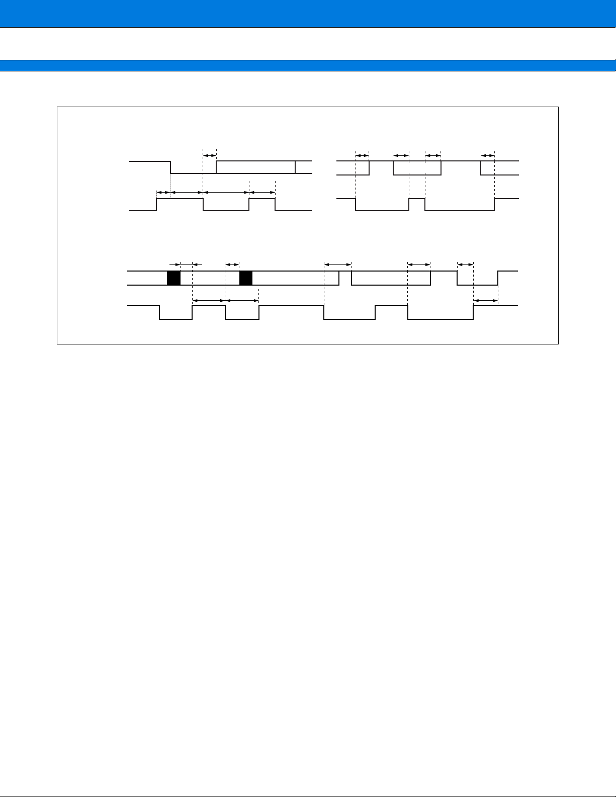
(5) Serial I/O Timing
Parameter
Symbol Pin Condition
(AV
CC = VCC = 3.0 V, AVSS = VSS = 0.0 V, TA = −40 °C to +85 °C)
Value
Min Max
Unit
Serial clock cycle time t
SCK ↓ → SO time t
SCYC SCK0, SCK1
SLOV SCK0, SCK1, SO0, SO1 −200 200 ns
Internal
2 tinst* µs
shift clock
Valid SI → SCK ↑ tIVSH SI0, SI1, SCK0, SCK1 1/2 tinst* µs
SCK ↑ → valid SI hold time t
Serial clock “H” pulse width t
SHIX SCK0, SCK1, SI0, SI1 1/2 tinst* µs
SHSL
mode
inst* µs
1 t
SCK0, SCK1
Serial clock “L” pulse width tSLSH 1 tinst* µs
SCK ↓ → SO time t
Valid SI → SCK ↑ t
SLOV SCK0, SCK1, SO0, SO1 0 200 ns
IVSH SI0, SI1, SCK0, SCK1 1/2 tinst* µs
External
shift clock
mode
SCK ↑ → valid SI hold time tSHIX SCK0, SCK1, SI0, SI1 1/2 tinst* µs
* : For information on t
inst, see “ (4) Instruction Cycle.”
Internal Clock Operation
SCYC
t
SCK0, SCK1
SO0, SO1
0.8 V
tSLOV
2.4 V
2.4 V
0.8 V
SI0, SI1
External Clock Operation
SCK0, SCK1
SO0, SO1
SI0, SI1
0.2 VCC
0.8 V
tSLSH
tSLOV
2.4 V
0.8 V
tIVSH
0.8 VCC
0.2 VCC
0.2 VCC
tIVSH
0.8 VCC
0.2 VCC
tSHIX
0.8 VCC
tSHIX
0.8 VCC
0.2 VCC
tSHSL
0.8 VCC
0.8 VCC
0.2 VCC
38

(6) I
2
C Timing
Parameter
Symbol Pin
MB89490 Series
(V
CC = 3.0V, AVSS = VSS = 0.0 V, TA = −40 °C to +85 °C)
Value
Min Max
Unit Remarks
Start condition output t
Stop condition output t
STA
STO
Start condition detect tSTA
Stop condition detect t
Re-start condition
output
Re-start condition
detect
SCL output LOW width t
SCL output HIGH width t
SDA output delay t
SDA output setup
time after interrupt
SCL input LOW
pulse width
STO
t
STASU
t
STASU
LOW SCL
HIGH SCL
DO SDA 1/4 tinst × 4 − 20 1/4 tinst × 4 + 20 ns
tDOSU SDA 1/4 tinst × 4 − 20 ns *4
t
LOW SCL 1/4 tinst × 6 + 40 ns
SCL
SDA
SCL
SDA
SCL
SDA
SCL
SDA
SCL
SDA
SCL
SDA
1/4 tinst*1 ×
M × N − 20
1/4 tinst ×
(M × N + 8) − 20
1/4 tinst ×
M × N + 20
1/4 tinst ×
2
(M*
× N*3 + 8) + 20
1/4 tinst × 6 + 40 ns
1/4 tinst × 6 + 40 ns
1/4 tinst ×
(M × N + 8) − 20
1/4 tinst ×
(M × N + 8) + 20
1/4 tinst × 4 + 40 ns
1/4 tinst ×
M × N − 20
1/4 tinst ×
(M × N + 8) − 20
1/4 tinst ×
M × N + 20
1/4 tinst ×
(M × N + 8) + 20
ns At master mode
ns At master mode
ns At master mode
ns At master mode
ns At master mode
SCL input HIGH
pulse width
t
HIGH SCL 1/4 tinst × 2 + 40 ns
SDA input setup time tSU SDA 40 ns
SDA hold time t
*1 : For information in t
*2 : M is defined in the I
HO SDA 0 ns
inst, see “ (4) Instruction Cycle”.
2
C clock control register ICCR bit 4 and bit 3 (CS4 and CS3). For details, please refer to
the H/W manual register explanation.
*3 : N is defined in the I
2
C clock control register ICCR bit 2 to bit 0 (CS2 to CS0).
*4 : When the interrupt period is greater than SCL “L” width, SDA and SCL output (Standard) value is based on
hypothesis when rising time is 0 ns.
39
MB89490 Series
Data transmit (master/slave)
SDA
tSTASU
SCL
Data receive (master/slave)
SU
t
SDA
SCL
67 8 9
tDO
tHOtLOWtSTA
1
tHO tDO tDO tDOSU
tHIGH tLOW
DO tHOtSU tDOSU
t
ACK
ACK
9
tSTO
40
(7) Peripheral Input Timing
Parameter
(AV
CC = VCC = 3.0 V, AVSS = VSS = 0.0 V, TA = −40 °C to +85 °C)
Symbol Pin
MB89490 Series
Value
Unit Remarks
Min Max
Peripheral input “H” pulse width 1 t
Peripheral input “L” pulse width 1 t
* : For information on t
EC0, EC1,
INT00 to INT07
INT10 to INT17
inst, see “ (4) Instruction Cycle.”
ILIH1
IHIL1 2 tinst* µs
0.2 VCC
0.5 VCC
EC0, EC1, INT00 to
INT07, INT10
tIHIL1
tIHIL1
to INT17
0.2 VCC
0.5 VCC
0.8 VCC
0.85 VCC
2 tinst* µs
tILIH1
0.8 VCC
tILIH1
0.85 VCC
41

MB89490 Series
5. A/D Converter Electrical Characteristics
(1) A/D Converter Electrical Characteristics
(AV
CC = VCC = 2.7 V to 3.6 V, AVSS = VSS = 0.0 V, TA = −40 °C to +85 °C)
Parameter Symbol Pin
Value
Unit Remarks
Min Typ Max
Resolution
10 bit
Total error ±3.0 LSB
Linearity error ±2.5 LSB
Differential linearity error ±1.9 LSB
Zero transition voltage V
Full-scale transition
voltage
OT
V
FST
A/D mode conversion time 30 t
Analog port input current I
Analog input voltage V
AIN
AN0 to
AN7
AIN AVSS AVR V
Reference voltage
I
R 95.0 170.0 µA
Reference voltage supply
AVR
AVSS −
1.5 LSB
AVCC −
3.5 LSB
inst* µs
AVSS +
0.5 LSB
AVCC −
1.5 LSB
AVSS +
2.5 LSB
AVCC −
0.5 LSB
10 µA
AV
SS + 2.7 AVCC V
mV
mV
current
I
RH 4.0 µA
* : For information on t
inst, see “ (4) Instruction Cycle” in “4. AC Characteristics”.
A/D is
activated
A/D is
stopped
42
MB89490 Series
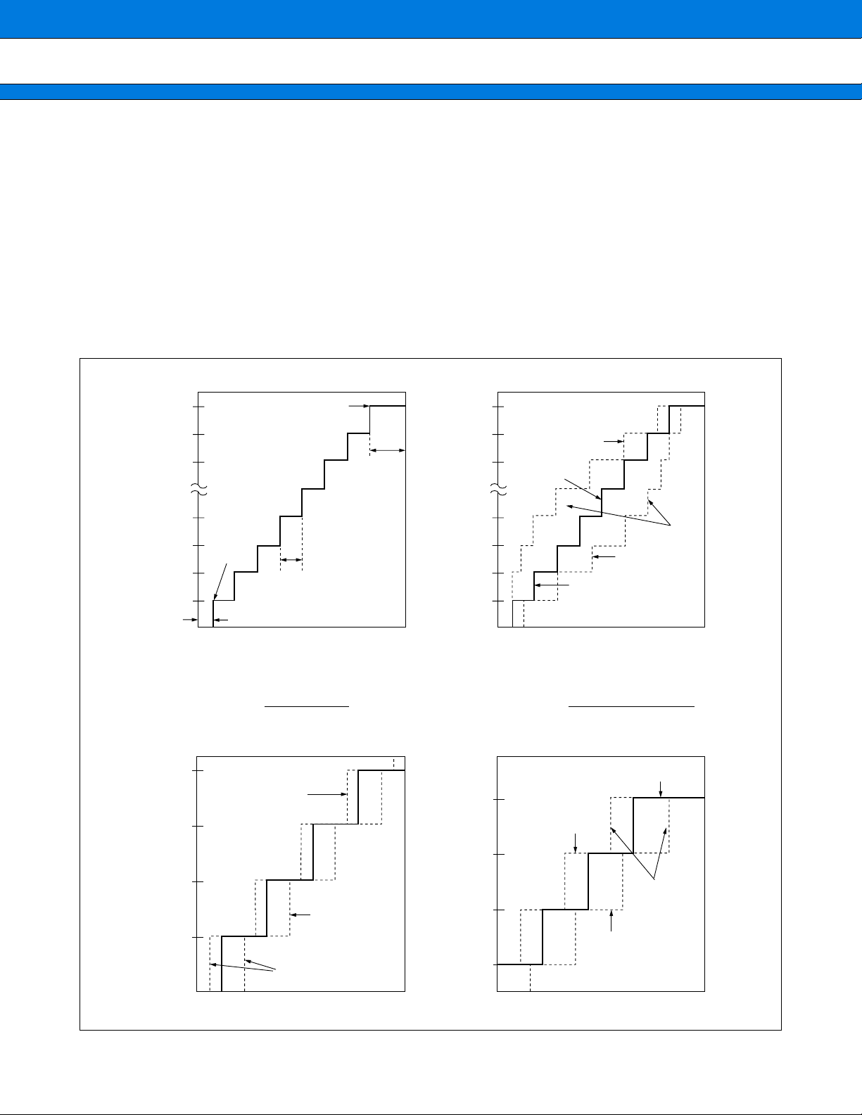
(2) A/D Converter Glossary
• Resolution
Analog changes that are identifiable with the A/D converter.
When the number of bits is 10, analog voltage can be divided into 2
• Linearity error (unit : LSB)
The deviation of the straight line connecting the ze ro transition point (“00 0000 0000” ↔ “00 0000 0001”) with
the full-scale transition point (“11 1111 1111” ↔ “11 1111 1110”) from actual conversion characteristics.
• Differential linearity error (unit : LSB)
The deviation of input voltage needed to change the output code by 1 LSB from the theoretical value.
• Total error (unit : LSB)
The difference between theoretical and actual conversion values.
10
= 1024.
3FF
H
3FE
H
3FD
H
004
H
Digital output
003
H
002
H
001
H
AV
004
H
003
H
Theoretical I/O characteristics
V
OT
1 LSB
0.5 LSB
SS
Analog input
FST
− V
OT
1 LSB =
V
1022
Zero transition error
Actual conversion
characteristics
Total error
V
FST
1.5 LSB
AV
CC
3FF
H
3FE
H
3FD
H
004
H
Digital output
003
H
002
H
001
H
AV
Actual conversion
characteristics
{1 LSB × N + VOT}
SS
Actual conversion
characteristics
Ideal characteristics
V
NT
AV
CC
Analog input
(V)
Total error =
VNT − {1 LSB × N + 0.5 LSB}
1 LSB
Full-scale transition error
Theoretical characteristics
3FF
H
Actual conversion
characteristics
002
H
Digital output
001
H
AV
3FE
H
FST
V
(Actual
measurement
value)
Actual conversion
characteristics
Digital output
3FD
H
Actual conversion
characteristics
3FC
V
OT
(Actual measurement
H
value)
AV
SS
Analog input
Analog input
CC
(Continued)
43

MB89490 Series
(Continued)
3FF
H
3FE
H
3FD
H
004
H
003
H
Digital output
002
H
001
H
AV
Actual conversion
characteristics
{1 LSB × N + VOT}
VOT (Actual measurement value)
SS
Linearity error =
Linearity error
Actual conversion
characteristics
Ideal value
Analog input
NT
− {1 LSB × N + VOT}
V
1 LSB
VNT
V
FST
(Actual
measurement
value)
AV
CC
N + 1
N
Digital output
N – 1
N – 2
AV
Differential linearity error
Actual conversion
characteristics
Actual conversion
characteristics
SS
Analog input
Differential linearity error =
Ideal value
V
NT
(N + 1)T
V
1 LSB
− V
V
(N + 1)T
NT
AV
− 1
CC
44

MB89490 Series
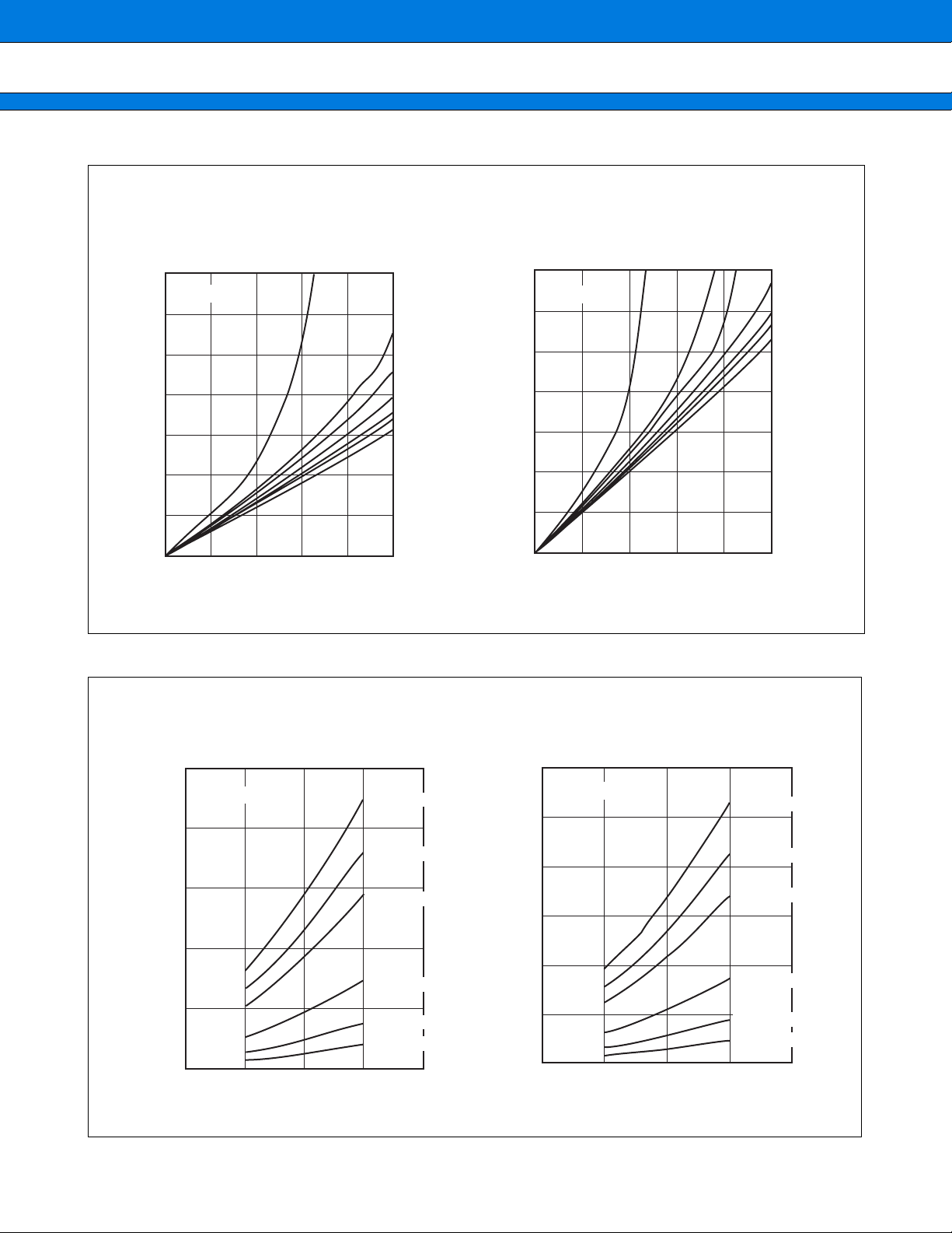
(3) Notes on Using A/D Converter
••••
About the external impedance of the analog input and its sampling time
• A/D converter with sample and hold circuit. If the external impedance is too high to keep sufficient sampling
time, the analog voltage charged to the internal sample and hold capacitor is insufficient, adversely affecting
A/D conversion precision.
Analog input circuit model
••••
R
Analog input
During sampling : ON
Note : The values are reference values.
C
MB89498 2.4 kΩ (Max) 44.0 pF (Max)
MB89F499 2.4 kΩ (Max) 28.6 pF (Max)
Comparator
RC
• To satisfy the A/D conversion precision standard, consider the relationship between the external impedance
and minimum sampling time and either adjust the resistor value and operating frequency or decrease the
external impedance so that the sampling time is longer than the minimum value.
The relationship between external impedance and minimum sampling time
••••
(External impedance = 0 kΩ to 100 kΩ)
100
90
80
70
60
50
40
30
20
External impedance [kΩ]
10
0
0 5 10 15 20 25 30 35
MB89F499 MB89498
Minimum sampling time [µs]
External impedance [kΩ]
(External impedance = 0 kΩ to 20 kΩ)
20
18
16
14
12
10
8
6
4
2
0
012345 78
MB89F499 MB89498
6
Minimum sampling time [µs]
• If the sampling time cannot be sufficient, connect a capacitor of about 0.1 µF to the analog input pin.
• About errors
As |AVRH − AV
SS| becomes smaller, values of relative errors grow larger.
45

MB89490 Series
EXAMPLE CHARACTERISTICS
■
(1) “L” level output voltage
0.25
TA = + 25˚C
0.20
0.15
VOL [V]
0.10
0.05
0.00
01024 86
VOL vs IOL (MB89498)
IOL [mA]
VCC = 2.0 V
VCC = 2.5 V
V
CC = 2.7 V
CC = 3.0 V
V
V
CC = 3.3 V
V
CC = 3.5 V
CC = 4.0 V
V
Port 0
VOL vs IOL (MB89F499)
0.30
TA = + 25˚C
0.25
0.20
0.15
VOL [V]
0.10
0.05
0.00
01024 86
IOL [mA]
VCC = 2.0 V
CC = 2.5 V
V
V
CC = 2.7 V
VCC = 3.0 V
VCC = 3.3 V
VCC = 3.5 V
V
CC = 4.0 V
Port 0
0.20
TA = + 25˚C
0.16
0.12
VOL [V]
0.08
0.02
0.00
01024 86
VOL vs IOL (MB89498)
IOL [mA]
VCC = 2.0 V
VCC = 2.5 V
VCC = 2.7 V
VCC = 3.0 V
V
CC = 3.3 V
V
CC = 3.5 V
CC = 4.0 V
V
Port 4
0.20
TA = + 25˚C
0.16
0.12
VOL [V]
0.08
0.04
0.00
01024 86
VOL vs IOL (MB89F499)
IOL [mA]
VCC = 2.0 V
VCC = 2.5 V
VCC = 2.7 V
V
CC = 3.0 V
VCC = 3.3 V
V
CC = 3.5 V
V
CC = 4.0 V
Port 4
(Continued)
46

(Continued)
MB89490 Series
VOL vs IOL (MB89498)
0.8
TA = + 25˚C
0.6
0.4
VOL [V]
0.2
0.0
01024 86
IOL [mA]
(2) “H” level output voltage
VCC = 2.0 V
VCC = 2.5 V
V
CC = 2.7 V
V
CC = 3.0 V
V
CC = 3.3 V
VCC = 3.5 V
V
CC = 4.0 V
Other than port 0, port 4
VOL vs IOL (MB89F499)
0.8
TA = + 25˚C
0.6
0.4
VOL [V]
0.2
0.0
01024 86
IOL [mA]
VCC = 2.0 V
VCC = 2.5 V
V
CC = 2.7 V
VCC = 3.0 V
VCC = 3.3 V
V
CC = 3.5 V
VCC = 4.0 V
Other than port 0, port 4
VCC - VOH vs IOH (MB89498)
0.7
TA = + 25˚C
0.6
0.5
0.4
0.3
VCC - VOH [V]
0.2
0.1
0.0
0 −10−2 −4 −8−6
IOH [mA]
VCC = 2.0 V
VCC = 2.5 V
V
CC = 2.7 V
CC = 3.0 V
V
CC = 3.3 V
V
V
CC = 3.5 V
CC = 4.0 V
V
Port 0
VCC − VOH vs IOH (MB89F499)
1.0
TA = + 25˚C
0.8
0.6
VCC - VOH [V]
0.4
0.2
0.0
0 −10−2 −4 −8−6
IOH [mA]
VCC = 2.0 V
VCC = 2.5 V
V
VCC = 3.0 V
V
V
VCC = 4.0 V
Port 0
CC = 2.7 V
CC = 3.3 V
CC = 3.5 V
(Continued)
47
MB89490 Series
(Continued)
VCC - VOH vs IOH (MB89498)
1.4
TA = + 25˚C
1.2
1.0
0.8
0.6
VCC = 2.0 V
VCC - VOH [V]
0.4
0.2
0.0
0 −10−2 −4 −8−6
IOH [mA]
Other than port 0
(3) Power supply current (External clock)
VCC = 2.5 V
V
CC = 2.7 V
V
CC = 3.0 V
V
CC = 3.3 V
V
CC = 3.5 V
CC = 4.0 V
V
VCC - VOH vs IOH (MB89F499)
1.4
TA = + 25˚C
1.2
1.0
0.8
0.6
VCC - VOH [V]
0.4
0.2
0.0
0 −10−2 −4 −8−6
VCC = 2.0 V VCC = 2.5 V VCC = 2.7 V
V
CC = 3.0 V
V
CC = 3.3 V
CC = 3.5 V
V
V
CC = 4.0 V
IOH [mA]
Other than port 0
48
ICC1 vs VCC (MB89498)
10.0
TA = + 25˚C
8.0
6.0
4.0
ICC1 [mA]
2.0
0.0
15234
VCC [V]
FCH = 12.5 MHz
F
CH = 10.0 MHz
F
CH = 8.0 MHz
F
CH = 4.0 MHz
F
CH = 2.0 MHz
F
CH = 1.0 MHz
ICC1 vs VCC (MB89F499)
12.0
TA = + 25˚C
10.0
8.0
6.0
ICC1 [mA]
4.0
2.0
0.0
15234
VCC [V]
FCH = 12.5 MHz
FCH = 10.0 MHz
F
CH = 8.0 MHz
F
CH = 4.0 MHz
F
CH = 2.0 MHz
F
CH = 1.0 MHz
(Continued)

MB89490 Series
ICCS1 vs VCC (MB89498)
4.5
TA = + 25˚C
4.0
3.5
3.0
2.5
2.0
ICCS1 [mA]
1.5
1.0
0.5
0.0
15234
VCC [V]
ICC2 vs VCC (MB89498)
FCH = 12.5 MHz
F
CH = 10.0 MHz
F
CH = 8.0 MHz
F
CH = 4.0 MHz
F
CH = 2.0 MHz
F
CH = 1.0 MHz
ICCS1 vs VCC (MB89F499)
4.0
TA = + 25˚C
3.5
3.0
2.5
2.0
ICCS1 [mA]
1.5
1.0
0.5
0.0
15234
VCC [V]
ICC2 vs VCC (MB89F499)
FCH = 12.5 MHz
F
CH = 10.0 MHz
F
CH = 8.0 MHz
F
CH = 4.0 MHz
F
CH = 2.0 MHz
F
CH = 1.0 MHz
1.4
TA = + 25˚C
1.2
1.0
0.8
0.6
ICC2 [mA]
0.4
0.2
0.0
15234
VCC [V]
FCH = 12.5 MHz
F
CH = 10.0 MHz
F
CH = 8.0 MHz
F
CH = 4.0 MHz
F
CH = 2.0 MHz
F
CH = 1.0 MHz
1.4
TA = + 25˚C
1.2
1.0
0.8
0.6
ICC2 [mA]
0.4
0.2
0.0
15234
VCC [V]
FCH = 12.5 MHz
FCH = 10.0 MHz
F
CH = 8.0 MHz
F
CH = 4.0 MHz
F
CH = 2.0 MHz
F
CH = 1.0 MHz
(Continued)
49
MB89490 Series
ICCS2 vs VCC (MB89498)
1.0
TA = + 25˚C
0.8
0.6
0.4
ICCS2 [mA]
0.2
0.0
15234
VCC [V]
FCH = 12.5 MHz
F
CH = 10.0 MHz
F
CH = 8.0 MHz
F
CH = 4.0 MHz
F
CH = 2.0 MHz
CH = 1.0 MHz
F
ICCS2 vs VCC (MB89F499)
1.0
TA = + 25˚C
0.8
0.6
0.4
ICCS2 [mA]
0.2
0.0
15234
VCC [V]
FCH = 12.5 MHz
FCH = 10.0 MHz
F
CH = 8.0 MHz
F
CH = 4.0 MHz
F
CH = 2.0 MHz
F
CH = 1.0 MHz
ICCLPLL vs VCC (MB89498)
0.30
TA = + 25˚C
0.25
0.20
0.15
ICCLPLL [mA]
0.10
0.05
0.00
15234
VCC [V]
FCH = 12.5 MHz
F
CH = 10.0 MHz
F
CH = 8.0 MHz
F
CH = 4.0 MHz
FCH = 2.0 MHz
F
CH = 1.0 MHz
ICCLPLL vs VCC (MB89F499)
0.30
TA = + 25˚C
0.25
0.20
0.15
ICCLPLL [mA]
0.10
0.05
0.00
15234
VCC [V]
FCH = 12.5 MHz
FCH = 10.0 MHz
F
CH = 8.0 MHz
F
CH = 4.0 MHz
F
CH = 2.0 MHz
FCH = 1.0 MHz
(Continued)
50

MB89490 Series
ICCL vs VCC (MB89498)
60.0
TA = + 25˚C
50.0
FCL = 32.768 kHz
40.0
30.0
ICCL [µA]
20.0
10.0
0.0
15234
VCC [V]
ICCL vs VCC (MB89F499)
60.0
TA = + 25˚C
50.0
FCL = 32.768 kHz
40.0
30.0
ICCL [µA]
20.0
10.0
0.0
15234
VCC [V]
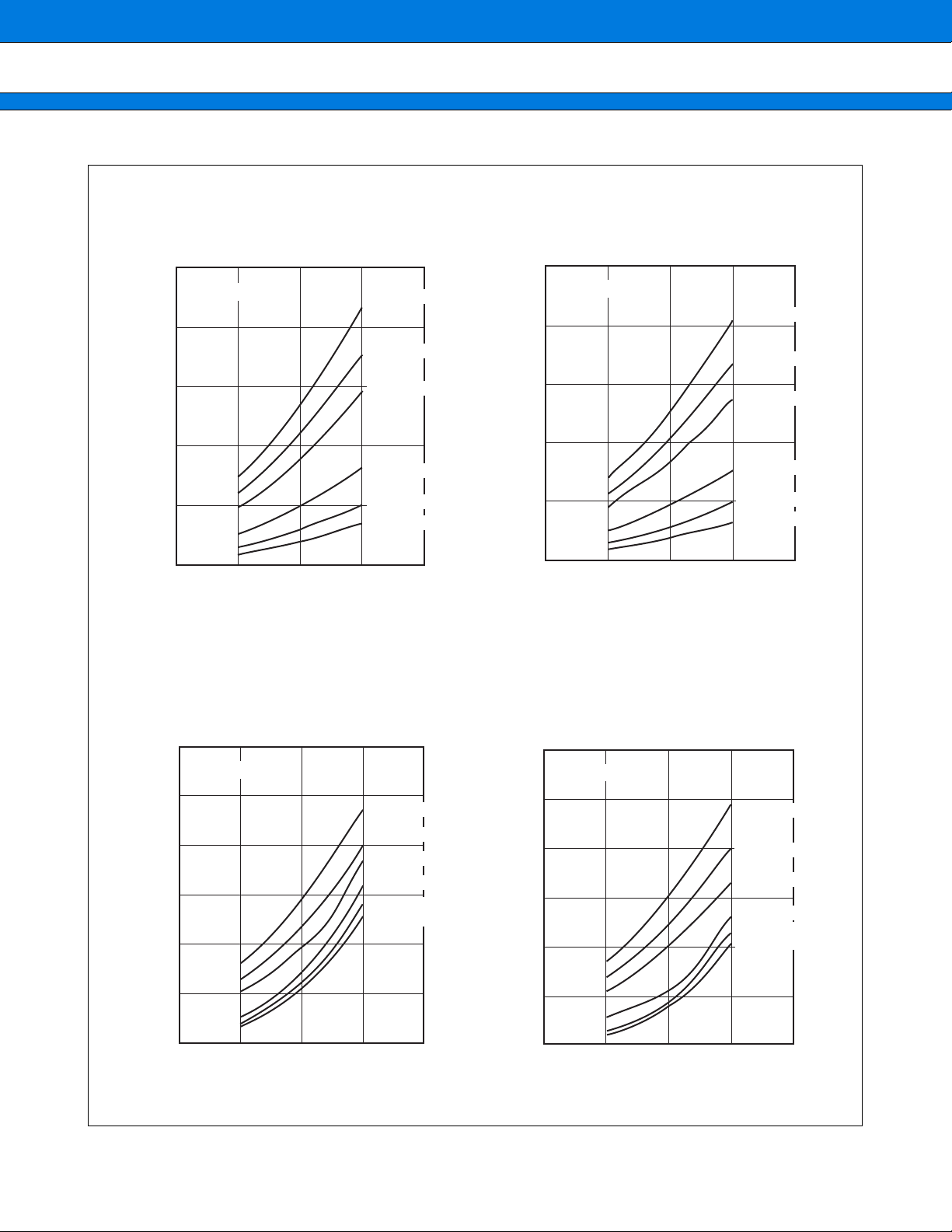
ICCLS vs VCC (MB89498)
20.0
TA = + 25˚C
16.0
FCL = 32.768 kHz
12.0
ICCLS [µA]
8.0
4.0
0.0
15234
VCC [V]
ICCLS vs VCC (MB89F499)
20.0
TA = + 25˚C
16.0
FCL = 32.768 kHz
12.0
ICCLS [µA]
8.0
4.0
0.0
15234
VCC [V]
(Continued)
51

MB89490 Series
(Continued)
ICCT vs VCC (MB89498)
2.0
TA = + 25˚C
1.6
FCL = 32.768 kHz
1.2
ICCT [µA]
0.8
0.4
0.0
15234
(4) Pull-up resistance
VCC [V]
ICCT vs VCC (MB89F499)
2.0
TA = + 25˚C
1.6
FCL = 32.768 kHz
1.2
ICCT [µA]
0.8
0.4
0.0
15234
VCC [V]
200
TA = + 25˚C
160
120
RPULL [kΩ]
80
45
0
1.5 3.52.0 2.5 3.0
RPULL vs VCC (MB89498)
VCC [V]
TA = + 110 ˚C
A = + 25 ˚C
T
T
A = - 40 ˚C
4.54.0
RPULL vs VCC (MB89F499)
120
TA = + 25˚C
100
80
60
RPULL [kΩ]
40
20
0
2.0 4.52.5 3.0 4.0
VCC [V]
3.5
TA = + 110 ˚C
T
A = + 25 ˚C
T
A = - 40 ˚C
52

MASK OPTIONS
■
Specifying procedure
MB89490 Series
Part number MB89498 MB89F499 MB89PV490
Specify when
ordering mask
Setting not possible
Main clock oscillation stabilizationtime selection
ORDERING INFORMATION
■
Part number Package Remarks
MB89498PF
MB89F499PF
MB89498PFV
MB89F499PFV
MB89PV490CF
10
2
/FCH
214/FCH
218/FCH
100-pin Plastic LQFP
100-pin Ceramic MQFP
Selectable
100-pin Plastic QFP
(FPT-100P-M06)
(FPT-100P-M05)
(MQP-100C-P01)
Fixed to oscillation stabilization wait
time of 2
18
/FCH
53

MB89490 Series
PACKAGE DIMENSIONS
■
100-pin Ceramic MQFP
(MQP-100C-P01)
18.70(.736)TYP
16.30±0.33
(.642±.013)
15.58±0.20
(.613±.008)
24.70(.972)
TYP
INDEX AREA
1.27±0.13
(.050±.005)
22.30±0.33
(.878±.013)
0.30(.012)
TYP
12.02(.473)
10.16(.400)
TYP
TYP
14.22(.560)
18.12±0.20
(.713±.008)
TYP
+0.40
–0.20
1.20
+.016
.047 –.008
12.35(.486)TYP
0.65±0.15
(.0256±.0060)
0.65±0.15
(.0256±.0060)
18.85(.742)
TYP
1.27±0.13
(.050±.005)
C
1994 FUJITSU LIMITED M100001SC-1-2
0.30(.012)TYP
7.62(.300)TYP
9.48(.373)TYP
11.68(.460)TYP
10.82(.426)
0.15±0.05
(.006±.002)
MAX
0.30±0.08
(.012±.003)
0.30±0.08
(.012±.003)
+0.40
–0.20
1.20
+.016
.047 –.008
Dimensions in mm (inches) .
Note : The values in parentheses are reference values.
(Continued)
54
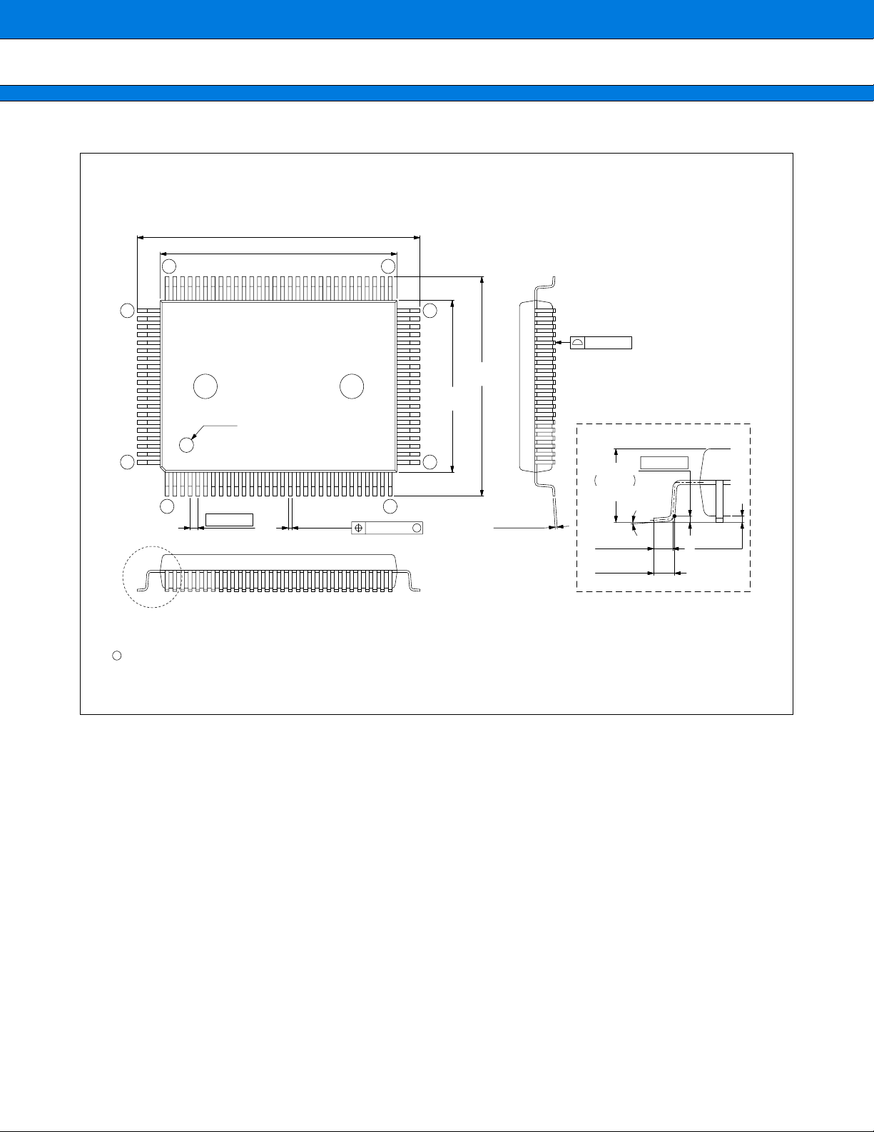
MB89490 Series
100-pin Plastic QFP
(FPT-100P-M06)
*
81
INDEX
100
1 30
0.65(.026)
"A"
23.90±0.40(.941±.016)
20.00±0.20(.787±.008)
0.32±0.05
(.013±.002)
Note 1) * : These dimensions do not include resin protrusion.
Note 2) Pins width and pins thickness include plating thickness.
Note 3) Pins width do not include tie bar cutting remainder.
5180
50
0.10(.004)
17.90±0.40
(.705±.016)
*
14.00±0.20
(.551±.008)
Details of "A" part
0.13(.005)
31
M
0.17±0.06
(.007±.002)
3.00
.118
(Mounting height)
(.031±.008)
(.035±.006)
+0.35
–0.20
+.014
–.008
0~8
0.80±0.20
0.88±0.15
0.25(.010)
˚
0.25±0.20
(.010±.008)
(Stand off)
C
2002 FUJITSU LIMITED F100008S-c-5-5
Dimensions in mm (inches) .
Note : The values in parentheses are reference values.
(Continued)
55

MB89490 Series
(Continued)
100-pin Plastic LQFP
(FPT-100P-M05)
16.00±0.20(.630±.008)SQ
*
14.00±0.10(.551±.004)SQ
75
76 50
INDEX
100
125
0.50(.020)
0.20±0.05
(.008±.002)
Note 1) * : These dimensions do not include resin protrusion.
Note 2) Pins width and pins thickness include plating thickness.
Note 3) Pins width do not include tie bar cutting remainder.
51
0.08(.003)
Details of "A" part
+.008
+0.20
.059
–.004
–0.10
1.50
0.08(.003)
(Mounting height)
26
"A"
M
0.145±0.055
(.0057±.0022)
0˚~8˚
0.50±0.20
(.020±.008)
0.60±0.15
(.024±.006)
0.10±0.10
(.004±.004)
(Stand off)
0.25(.010)
C
2003 FUJITSU LIMITED F100007S-c-4-6
Dimensions in mm (inches) .
Note : The values in parentheses are reference values.
56

MB89490 Series
FUJITSU LIMITED
All Rights Reserved.
The contents of this document are subject to change without notice.
Customers are advised to consult with FUJITSU sales
representatives before ordering.
The information, such as descriptions of function and application
circuit examples, in this document are presented solely for the
purpose of reference to show examples of operations and uses of
Fujitsu semiconductor device; Fujitsu does not warrant proper
operation of the device with respect to use based on such
information. When you develop equipment incorporating the
device based on such information, you must assume any
responsibility arising out of such use of the information. Fujitsu
assumes no liability for any damages whatsoever arising out of
the use of the information.
Any information in this document, including descriptions of
function and schematic diagrams, shall not be construed as license
of the use or exercise of any intellectual property right, such as
patent right or copyright, or any other right of Fujitsu or any third
party or does Fujitsu warrant non-infringement of any third-party’s
intellectual property right or other right by using such information.
Fujitsu assumes no liability for any infringement of the intellectual
property rights or other rights of third parties which would result
from the use of information contained herein.
The products described in this document are designed, developed
and manufactured as contemplated for general use, including
without limitation, ordinary industrial use, general office use,
personal use, and household use, but are not designed, developed
and manufactured as contemplated (1) for use accompanying fatal
risks or dangers that, unless extremely high safety is secured, could
have a serious effect to the public, and could lead directly to death,
personal injury, severe physical damage or other loss (i.e., nuclear
reaction control in nuclear facility, aircraft flight control, air traffic
control, mass transport control, medical life support system, missile
launch control in weapon system), or (2) for use requiring
extremely high reliability (i.e., submersible repeater and artificial
satellite).
Please note that Fujitsu will not be liable against you and/or any
third party for any claims or damages arising in connection with
above-mentioned uses of the products.
Any semiconductor devices have an inherent chance of failure. You
must protect against injury, damage or loss from such failures by
incorporating safety design measures into your facility and
equipment such as redundancy, fire protection, and prevention of
over-current levels and other abnormal operating conditions.
If any products described in this document represent goods or
technologies subject to certain restrictions on export under the
Foreign Exchange and Foreign Trade Law of Japan, the prior
authorization by Japanese government will be required for export
of those products from Japan.
F0410
2004 FUJITSU LIMITED Printed in Japan
 Loading...