

查询MB81P643287供应商
FUJITSU SEMICONDUCTOR
DATA SHEET
DS05-11402-2E
MEMORY
CMOS
TM
8 x 256K x 32 BIT, FCRAM
CORE
BASED DOUBLE DATA RATE SDRAM
MB81P643287-50/-60
CMOS 8-BANK x 262,144-WORD x 32 BIT, FCRAM Core Based
Synchronous Dynamic Random Access Memory
with Double Data Rate
DESCRIPTION
■■■■
The Fujitsu MB81P643287 is a CMOS Synchronous Dynamic Random Access Memory (SDRAM) with Fujitsu
advanced FCRAM (F ast Cycle Random Access Memory) Core Technology, containing 67,108,864 memory cells
accessible in an 32-bit format. The MB81P643287 features a fully synchronous operation referenced to clock
edge whereby all operations are synchronized at a cloc k input which enables high performance and simple user
interface coe xistence. The MB81P643287 is designed to reduce the complexity of using a standard dynamic RAM
(DRAM) which requires many control signal timin.g constraints. The MB81P643287 uses Double Data Rate (DDR)
where data bandwidth is twice of fast speed compared with regular SDRAMs.
The MB81P643287 is ideally suited for Digital Visual Systems, High Performance Graphic Adapters, Hardware
Accelerators, Buffers, and other applications where large memor y density and high effective bandwidth are
required and where a simple interface is needed.
The MB81P643287 adopts new I/O interface circuitry, SSTL_2 interface, which is capable of extremely fast data
transfer of quality under either terminated or point to point bus environment.
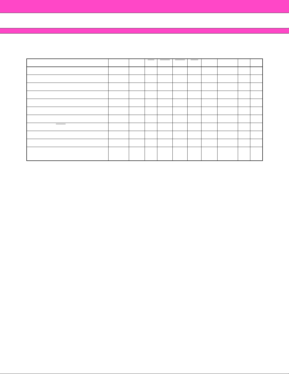
PRODUCT LINE
■■■■
Clock Frequency
Burst Mode Cycle Time
MB81P643287
Parameter
-50 -60
CL = 3 200 MHz Max. 167 MHz Max.
CL = 2 133 MHz Max. 111 MHz Max.
CL = 3 2.5 ns Min. 3.0 ns Min.
CL = 2 3.75 ns Min. 4.5 ns Min.
Random Address Cycle Time 30 ns Min. 36 ns Min.
DQS Access Time From Clock 0.1 × t
Operating Current 460 mA Max. 405 mA Max.
Power Down Current 35 mA Max.
Note: FCRAM is a trademark of Fujitsu Limited, Japan.
CK + 0.2 ns Max. 0.1 × tCK + 0.2 ns Max.

MB81P643287-50/-60
FEATURES
■■■■
• Double Data Rate
• Bi-directional Data Strobe Signal
• Eight bank operation
• Burst read/write operation
• Programmable burst length and CAS latency
• Byte write control by DM
• Standby Power Down Mode
PACKAGE
■■■■
0 to DM3
• 4096 Auto-refresh cycles in 32 ms
• SSTL_2 (class 2) for all signals
DD: +2.5V Supply ± 0.2V tolerance
•V
•VDDQ: +2.5V Supply ± 0.2V tolerance
86-pin plastic TSOP(II)
(FPT-86P-M01)
(Normal Bend)
2
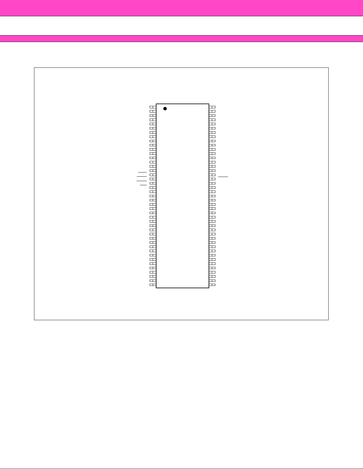
PIN ASSIGNMENTS
■■■■
MB81P643287-50/-60
86-pin TSOP (II)
(TOP VIEW)
(Normal Bend)
VDD
DQ0
VDDQ
DQ1
DQ2
VSSQ
DQ3
DQ4
VDDQ
DQ5
DQ6
VSSQ
DQ7
DQS0
VDD
DM0
WE
CAS
RAS
CS
BA
BA0
BA1
A10/AP
A
A1
A2
DM2
VDD
DQS2
DQ16
VSSQ
DQ17
DQ18
VDDQ
DQ19
DQ20
VSSQ
DQ21
DQ22
VDDQ
DQ23
VDD
1
2
3
4
5
6
7
8
9
10
11
12
13
14
15
16
17
18
19
20
2
21
22
23
24
0
25
26
27
28
29
30
31
32
33
34
35
36
37
38
39
40
41
42
43
86
85
84
83
82
81
80
79
78
77
76
75
74
73
72
71
70
69
68
67
66
65
64
63
62
61
60
59
58
57
56
55
54
53
52
51
50
49
48
47
46
45
44
VSS
DQ15
VSSQ
DQ14
DQ13
VDDQ
DQ12
DQ11
VSSQ
DQ10
DQ9
VDDQ
DQ8
DQS1
VSS
DM1
VREF
CLK
CLK
CKE
A
9
A8
A7
A6
A5
A4
A3
DM3
VSS
DQS3
DQ31
VDDQ
DQ30
DQ29
VSSQ
DQ28
DQ27
VDDQ
DQ26
DQ25
VSSQ
DQ24
VSS
(FPT-86P-M01)
3
MB81P643287-50/-60
DESCRIPTIONS
■■■■
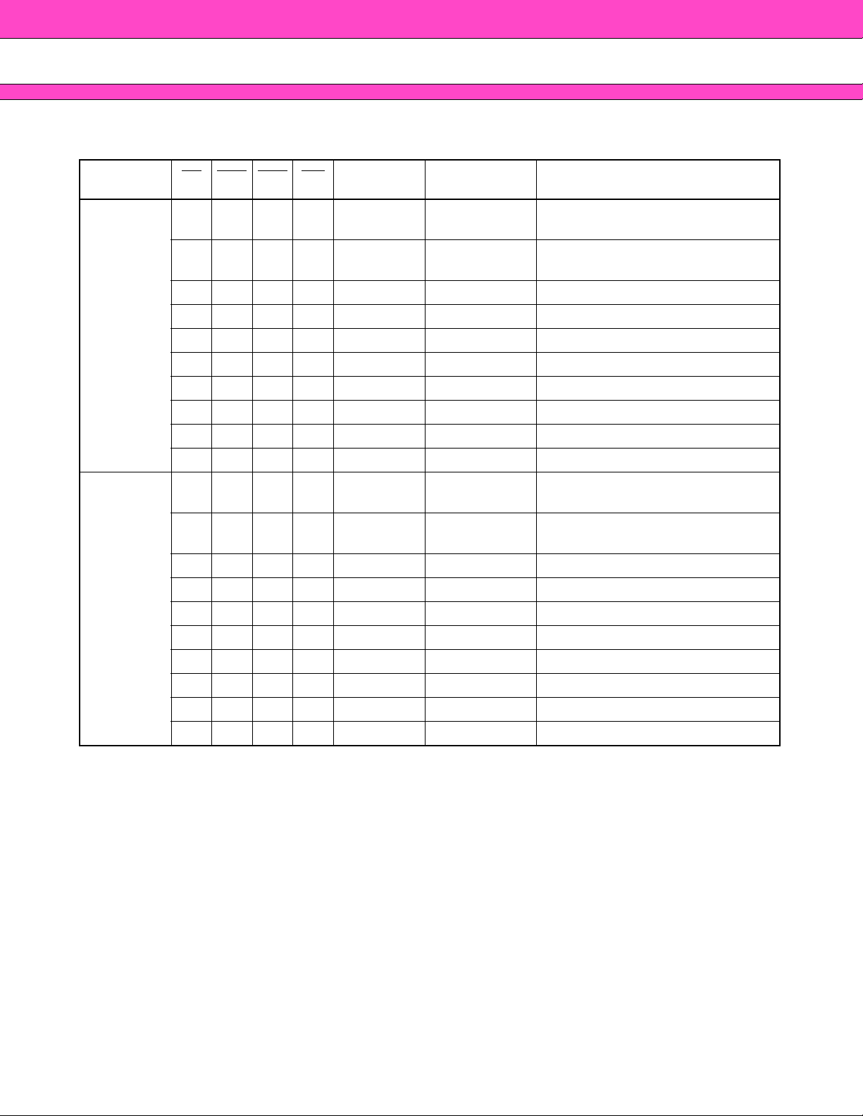
Pin Number Symbol Function
1, 3, 9, 15, 29, 35, 41, 43, 49, 55, 75, 81 V
DD, VDDQ Supply Voltage
6, 12, 32, 38, 44, 46, 52, 58, 72, 78, 84, 86 V
2, 4, 5, 7, 8, 10, 11, 13, 31, 33, 34, 36, 37, 39,
40, 42, 45, 47, 48, 50, 51, 53, 54, 56, 74, 76,
77, 79, 80, 82, 83, 85
14, 30, 57, 73 DQS0 to DQS3 Data Strobe
16, 28, 59, 71 DM0 to DM3 Input Mask
17 WE
18 CAS
19 RAS Row Address Strobe
20 CS
21, 22, 23 BA
24 AP Auto Precharge Enable
24, 25, 26, 27, 60, 61, 62, 63, 64, 65, 66 A
67 CKE Power Down
SS, VSSQ Ground
• Byte 0: DQ
0 to DQ31 Data I/O
DQ
• Byte 1: DQ8 to DQ15
• Byte 2: DQ16 to DQ23
• Byte 3: DQ24 to DQ31
•DQS
•DQS1: for DQ8 to DQ15
•DQS2: for DQ16 to DQ23
•DQS3: for DQ24 to DQ31
Write Enable
Column Address Strobe
Chip Select
2, BA1, BA0 Bank Select (Bank Address)
0 to A10 Address Input
•Row: A
• Column: A0 to A6
0 to DQ7
0: for DQ0 to DQ7
0 to A10
68 CLK Clock Input
69 CLK
Clock Input
70 VREF Input Reference Voltage
4
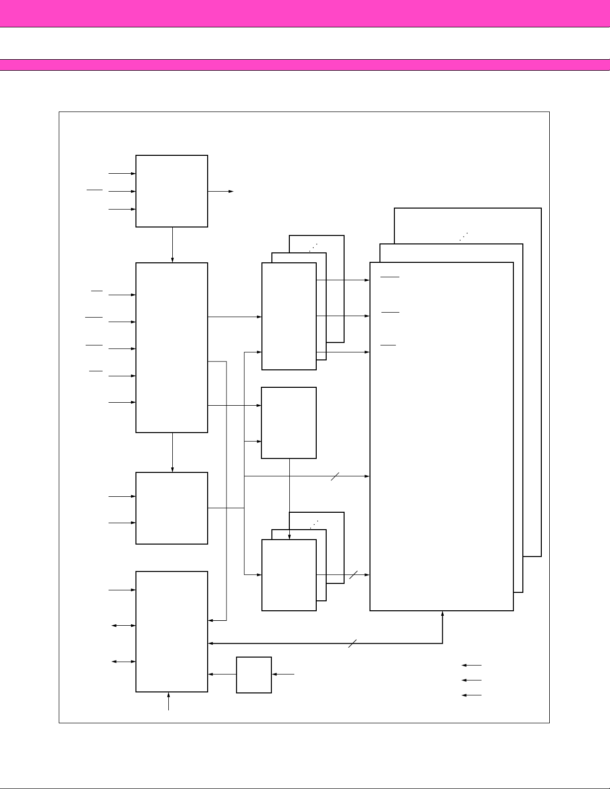
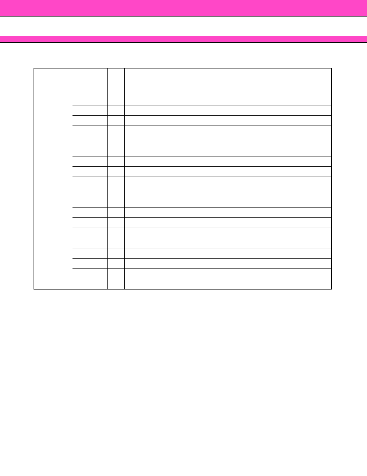
BLOCK DIAGRAM
■■■■
CLK
CLK
CLOCK
BUFFER
MB81P643287-50/-60
Fig. 1 - MB81P643287 BLOCK DIAGRAM
To each block
CKE
CS
RAS
CAS
WE
AP
A
0 to A10
BA0, BA1,
BA2
Enable
COMMAND
DECODER
ADDRESS
BUFFER/
REGISTER
CONTROL
SIGNAL
LATCH
MODE
REGISTER
11
RAS
CAS
WE
ROW
ADDRESS
Bank-7
Bank-1
Bank-0
DRAM
CORE
(2048 × 128 × 32)
DM0 to
DM3
DQ0 to
DQ
DQS0 to
DQS3
COLUMN
ADDRESS
COUNTER
I/O DATA
BUFFER/
31
REGISTER
&
DQS
GENERATOR
V
DDQ, VSSQ
DLL
Clock Buffer
32
7
COLUMN
ADDRESS
I/O
DD
V
VREF
VSS/VSSQ
5
MB81P643287-50/-60
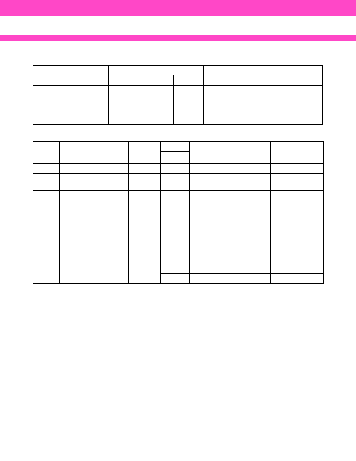
FUNCTION TRUTH TABLE (Note*1)
■■■■
MRS/
EMRS
2-0
RAS CAS WE BA
HLL LLV L VV
10/
A
AP A
9-7A6-0
COMMAND TRUTH TABLE (Note *2, and *3)
Function Notes Symbol CKE CS
Device Deselect *4 DESL H H X X X X X X X
No Operation *4 NOP H L H H H X X X X
Burst Stop *5 BST H L H H L X X X X
Read *6 READ H L H L H V L X V
Read with Auto-precharge *6 READA H L H L H V H X V
Write *6 WRIT H L H L L V L X V
Write with Auto-precharge *6 WRITA H L H L L V H X V
Bank Active (RAS
Precharge Single Bank *8 PRE H L L H L V L X X
Precharge All Banks *8 PALL H L L H L V H X X
Mode Register Set/
Extended Mode Register Set
)*7ACTVHLLHHVVVV
*8,9,10
Notes: *1. V = Valid, L = Logic Low, H = Logic High, X = either L or H, Hi-Z = High Impedance.
*2. All commands are assumed to be valid state transitions.
*3. All inputs for command are latched on the rising edge of clock(CLK).
*4. NOP and DESL commands have the same effect on the part.
Unless specifically noted, NOP will represent both NOP and DESL command in later descriptions.
*5. BST is effective after READ command is issued.
*6. READ , READ A, WRIT and WRITA commands should only be issued after the corresponding bank has
been activated (ACTV command). Refer to “■ STATE DIAGRAM”.
*7. ACTV command should only be issued after corresponding bank has been page closed by PRE or
PALL command.
*8. Either PRE or PALL command and MRS or EMRS command are required after power up.
*9. MRS or EMRS command should only be issued after all banks have been page closed (PRE or PALL
command), and DQs are in Hi-Z. Refer to “■ STATE DIAGRAM”.
*10. Refer to“■ MODE REGISTER TABLE”.
6
DM TRUTH TABLE (Effective during Write mode)
Function Command
(n - 1) (n)
CKE
MB81P643287-50/-60
DM
0
DM
1
DM
2
DM
3
Data Mask for DQ
Data Mask for DQ
Data Mask for DQ
0 to DQ7 MASK0HXHXXX
8 to DQ15 MASK1 H X X H X X
16 to DQ23 MASK2HXXXHX
Data Mask for DQ24 to DQ31 MASK3 H X X X X H
CKE TRUTH TABLE
0
Current
State
Function Notes Command
CKE
(n-1)
(n)
RAS CAS WE AP
CS
BA0
BA
to
A
to
2
DQ
10
A
Idle Auto-refresh *11 REF H H L L L H X X X —
Idle Self-refresh Entry
Self-
refresh
Self-
refresh
Self-refresh Continue — L L X X X X X X X Hi-Z
Self-refresh Exit SELFX
*11
*12
SELF H L L L L H X X X Hi-Z
LHL H H H X X XHi-Z
LHH X X X X X XHi-Z
HLL H H H X X XHi-Z
Idle Power Down Entry *13 PDEN
HLHX X X X X XHi-Z
Power
Down
Power Down Continue — L L X X X X X X X Hi-Z
DQ
to
0
31
Power
Down
Power Down Exit PDEX
LHL H H H X X XHi-Z
LHH X X X X X XHi-Z
*11: The REF and SELF commands should only be issued after all banks have been precharged (PRE or PALL
command). In case of SELF command, it should also be issued after the last read data have been appeared
on DQ. Refer to “■ STATE DIAGRAM”.
*12: CKE must bring to Low level together with REF command.
*13: The PDEN command should only be issued after the last read data have been appeared on DQ and after the
l
DPL is satisfied from last write data input.
7
MB81P643287-50/-60
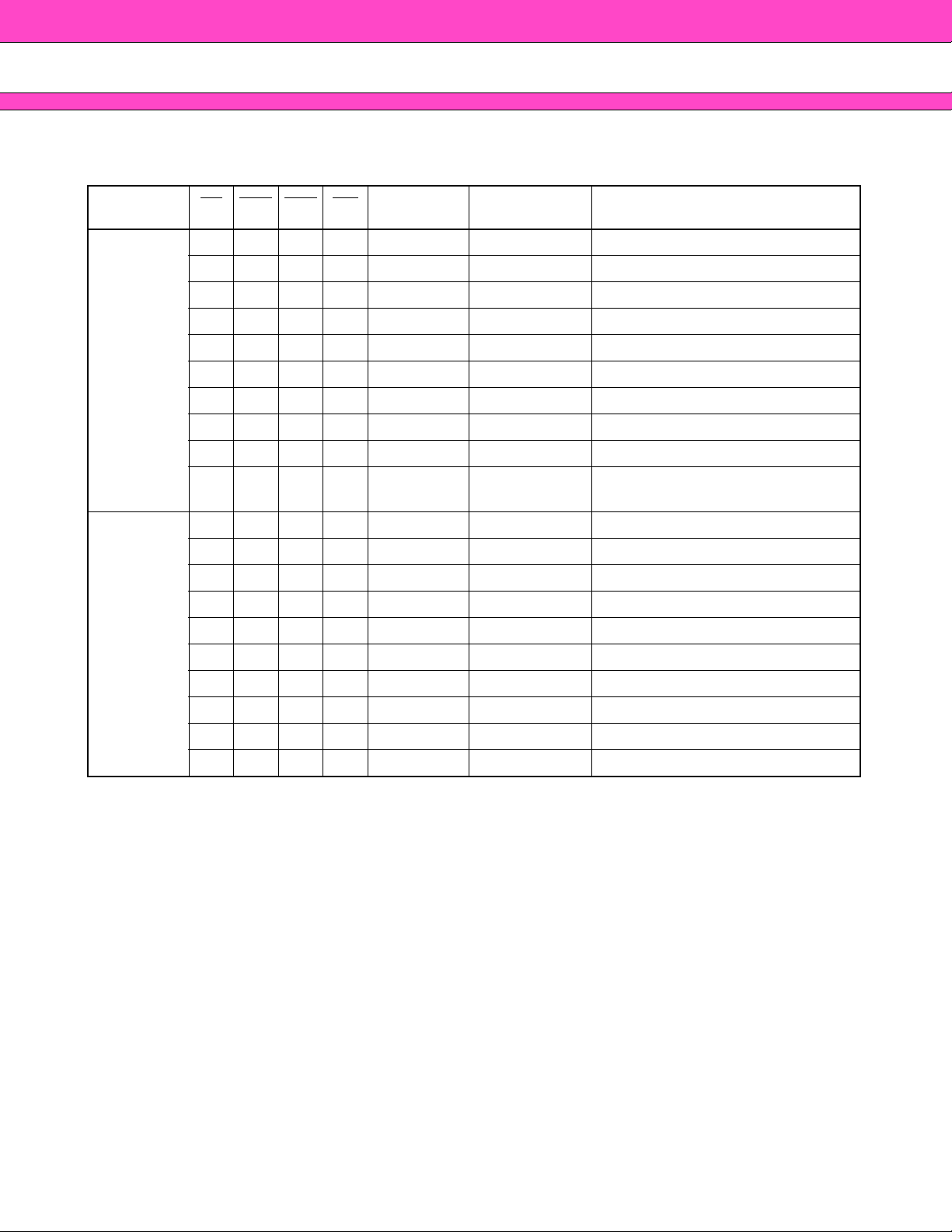
OPERATION COMMAND TABLE (Applicable to single bank)(Note*13)
Current
State
Idle
RAS CAS WE Address Command Function Notes
CS
HXXX X DESL NOP
LHHH X NOP NOP
L H H L X BST NOP *15
L H L H BA, CA, AP READ/READA Illegal *16
L H L L BA, CA, AP WRIT/WRITA Illegal *16
L L H H BA, RA ACTV Bank Active after l
L L H L BA, AP PRE NOP
L L H L BA, AP PALL NOP *15
L L L H X REF/SELF Auto-refresh or Self-refresh *17
RCD
Bank Active
LLLL MODE MRS
HXXX X DESL NOP
LHHH X NOP NOP
L H H L X BST NOP *15
L H L H BA, CA, AP READ/READA Begin Read; Determine AP
L H L L BA, CA, AP WRIT/WRITA Begin Write; Determine AP
L L H H BA, RA ACTV Illegal *16
L L H L BA, AP PRE Precharge
L L H L BA, AP PALL Precharge *15
L L L H X REF/SELF Illegal
LLLL MODE MRS Illegal
Mode Register Set
(Idle after l
MRD)
*17
8
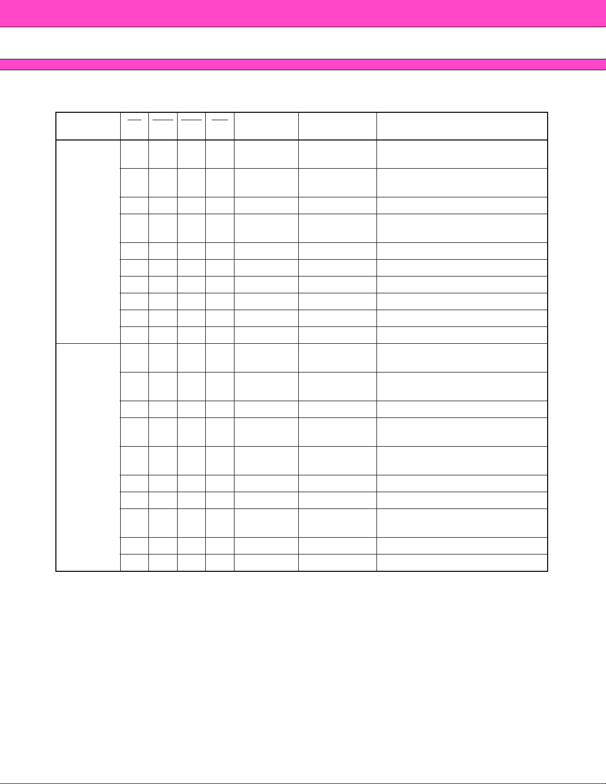
OPERATION COMMAND TABLE (Continued)
Current
State
CS
RAS CAS WE Address Command Function Notes
HXXX X DESL
MB81P643287-50/-60
NOP (Continue Burst to End →
Bank Active)
Read
Write
LHHH X NOP
L H H L X BST Terminate Burst → Bank Active
L H L H BA, CA, AP READ/READA
L H L L BA, CA, AP WRIT/WRITA Illegal
L L H H BA, RA ACTV Illegal *16
L L H L BA, AP PRE Terminate Burst, Precharge
L L H L BA, AP PALL Terminate Burst, Precharge *15
L L L H X REF/SELF Illegal
LLLL MODE MRS Illegal
HXXX X DESL
LHHH X NOP
L H H L X BST Illegal
L H L H BA, CA, AP READ/READA
L H L L BA, CA, AP WRIT/WRITA
NOP (Continue Burst to End →
Bank Active)
Terminate Burst, New Read;
Determine AP
NOP (Continue Burst to End →
Write Recovering)
NOP (Continue Burst to End →
Write Recovering)
Terminate Burst, Start Read;
Determine AP
Terminate Burst, New Write;
Determine AP
*20
L L H H BA, RA ACTV Illegal *16
L L H L BA, AP PRE Terminate Burst, Precharge *18
L L H L BA, AP PALL Terminate Burst, Precharge
L L L H X REF/SELF Illegal
LLLL MODE MRS Illegal
*15,
*18
9
MB81P643287-50/-60
OPERATION COMMAND TABLE (Continued)
Current
State
CS
RAS CAS WE Address Command Function Notes
HXXX X DESL
NOP (Continue Burst to End →
Precharge)
Read With
AutoPrecharge
Write with
Auto
Precharge
LHHH X NOP
L H H L X BST Illegal
L H L H BA, CA, AP READ/READA Illegal *16
L H L L BA, CA, AP WRIT/WRITA Illegal
L L H H BA, RA ACTV Illegal *16
L L H L BA, AP PRE Illegal *16
L L H L BA, AP PALL Illegal
L L L H X REF/SELF Illegal
LLLL MODE MRS Illegal
HXXX X DESL
LHHH X NOP
L H H L X BST Illegal
L H L H BA, CA, AP READ/READA Illegal
L H L L BA, CA, AP WRIT/WRITA Illegal *16
L L H H BA, RA ACTV Illegal *16
NOP (Continue Burst to End →
Precharge)
NOP (Continue Burst to End →
Write Recovering with Precharge)
NOP (Continue Burst to End →
Write Recovering with Precharge)
10
L L H L BA, AP PRE Illegal *16
L L H L BA, AP PALL Illegal
L L L H X REF/SELF Illegal
LLLL MODE MRS Illegal
OPERATION COMMAND TABLE (Continued)
Current
State
CS
RAS CAS WE Address Command Function Notes
H X X X X DESL NOP (Idle after l
MB81P643287-50/-60
RP)
Precharging
Bank
Activating
L H H H X NOP NOP (Idle after l
L H H L X BST NOP (Idle after l
RP)
RP)*15
L H L H BA, CA, AP READ/READA Illegal *16
L H L L BA, CA, AP WRIT/WRITA Illegal *16
L L H H BA, RA ACTV Illegal *16
L L H L BA, AP PRE NOP *16
L L H L BA, AP PALL NOP *15
L L L H X REF/SELF Illegal
LLLL MODE MRS Illegal
H X X X X DESL NOP (Bank Active after l
L H H H X NOP NOP (Bank Active after l
L H H L X BST NOP (Bank Active after l
RCD)
RCD)
RCD)*15
L H L H BA, CA, AP READ/READA Illegal *16
L H L L BA, CA, AP WRIT/WRITA Illegal *16
L L H H BA, RA ACTV Illegal *19
L L H L BA, AP PRE Illegal *16
L L H L BA, AP PALL Illegal
L L L H X REF/SELF Illegal
LLLL MODE MRS Illegal
11
MB81P643287-50/-60
OPERATION COMMAND TABLE (Continued)
Current
State
CS
RAS CAS WE Address Command Function Notes
Write
Recovering
Write
Recovering
with Autoprecharge
H X X X X DESL NOP (Bank Active after l
L H H H X NOP NOP (Bank Active after l
L H H L X BST NOP (Bank Active after l
WRD)
WRD)
WRD)*15
L H L H BA, CA, AP READ/READA Illegal *16
L H L L BA, CA, AP WRIT/WRITA New Write; Determine AP
L L H H BA, RA ACTV Illegal *16
L L H L BA, AP PRE Illegal *16
L L H L BA, AP PALL Illegal
L L L H X REF/SELF Illegal
LLLL MODE MRS Illegal
H X X X X DESL NOP (Idle after l
L H H H X NOP NOP (Idle after l
WAL)
WAL)
L H H L X BST Illegal
L H L H BA, CA, AP READ/READA Illegal *16
L H L L BA, CA, AP WRIT/WRITA Illegal *16
L L H H BA, RA ACTV Illegal *16
L L H L BA, AP PRE Illegal *16
L L H L BA, AP PALL Illegal
Refreshing
L L L H X REF/SELF Illegal
LLLL MODE MRS Illegal
H X X X X DESL NOP (Idle after l
L H H X X NOP/BST NOP (Idle after l
LHLX X
LLHX X
LLLX X
READ/READA/
WRIT/WRITA
ACTV/
PRE/PALL
REF/SELF/
MRS
Illegal
Illegal
Illegal
RFC)
RFC)
12
MB81P643287-50/-60
OPERATION COMMAND TABLE (Continued)
Current
State
Mode
Register
Setting
Abbreviations: RA = Row Address BA = Bank Address
Notes: *14. All entries assume the CKE was High during the proceeding clock cycle and the current clock cycle.
*15. Entry may affect other banks.
*16. Illegal to bank in specified state; entry may be legal in the bank specified by BA, depending on the state
*17. Illegal if any bank is not idle.
*18. Must mask preceding data that don‘t satisfy lDPL.
*19. Legal if other bank specified in BA is idle state and lRRD is satisfied for that bank.
*20. Must mask preceding data that don‘t satisfy lWRD.
CS
RAS CAS WE Address Command Function Notes
H X X X X DESL NOP (Idle after l
L H H H X NOP NOP (Idle after l
L H H L X BST Illegal
LHLX X
LLXX X
CA = Column Address AP = Auto Precharge
of that bank.
READ/READA/
WRIT/WRITA
ACTV/PRE/
PALL/REF/
SELF/MRS
MRD)
MRD)
Illegal
Illegal
13
MB81P643287-50/-60
COMMAND TRUTH TABLE FOR CKE
Current
State
Selfrefresh
CKE
(n-1)
CKE
(n)
RAS CAS WE Address Function Notes
CS
HXXXXX XInvalid
LHHXXX X
LHLHHH X
L H L H H L X Illegal
L H L H L X X Illegal
L H L L X X X Illegal
LLXXXX XNOP (Maintain Self-refresh)
LXXXXX XInvalid
H H H X X X X Idle after l
Exit Self-refresh
(Self-refresh Recovery →
Idle after t
PDEX + lSCD or lXSNR)
Exit Self-refresh
(Self-refresh Recovery →
Idle after t
PDEX + lSCD or lXSNR)
SCD or lXSNR
Selfrefresh
Recovery
Power
Down
H H L H H H X I dle after lSCD or lXSNR
H H L H H L X Illegal
H H L H L X X Illegal
H H L L X X X Illegal
HLXXXX XIllegal
HXXXXX XInvalid
LHHXXX X
LHLHHH X
Power Down Exit → Return to original
state after t
PDEX
Power Down Exit → Return to original
state after tPDEX
L H L H H L X Illegal
L H L H L X X Illegal
L H L L X X X Illegal
LLXXXX XNOP (Maintain Power Down Mode)
14
COMMAND TRUTH TABLE FOR CKE (continued)
Current
State
All
Banks
Idle
CKE
(n-1)
CKE
(n)
HHHXXX XNOP
H H L H X X V Refer to the Command Truth Table.
H H L L H X V Refer to the Command Truth Table.
H H L L L H X Auto-refresh
HHLLLL VMode Register Set *21
H L H X X X X Power Down Entry *22
H L L H H H X Power Down Entry *22
H L L H H L X Illegal
H L L H L X X Illegal
H L L L H X X Illegal
HLLLLH XSelf-refresh Entry *22
HLLLLL XIllegal
RAS CAS WE Address Function Notes
CS
MB81P643287-50/-60
Bank Active
LXXXXX XInvalid
HHXXXX XRefer to the Command Truth Table.
HLXXXX XIllegal
LHXXXX XInvalid
LLXXXX XInvalid
15
MB81P643287-50/-60
COMMAND TRUTH TABLE FOR CKE (continued)
Current
State
CKE
(n-1)
CKE
(n)
RAS CAS WE Address Function Notes
CS
Bank
Activating,
Read, Write,
Write
Recovering,
Precharging
Any State
Other Than
Listed Above
Refresh
Notes: *21. Refer to “■ MODE REGISTER TABLE”.
*22. PDEN and SELF command should only be issued after the last read data have been appeared on DQ.
*23. The Clock Suspend mode is not supported on this device and it is illegal if CKE is brought to Low during
HHXXXX XRefer to the Command Truth Table.
HLXXXX XIllegal *23
LHXXXX XInvalid
LLXXXX XInvalid
LXXXXX XInvalid
HHXXXX XRefer to the Command Truth Table.
HLXXXX XIllegal *23
H L H L L L X Illegal
H L L H H H X Illegal
H L L H H L X Illegal
H L L H L X X Illegal
H L L L X X X Illegal
LLXXXX XInvalid
LHXXXX XInvalid
HHXXXX XRefer to the Command Truth Table.
the Burst Read or Write mode.
16
MB81P643287-50/-60
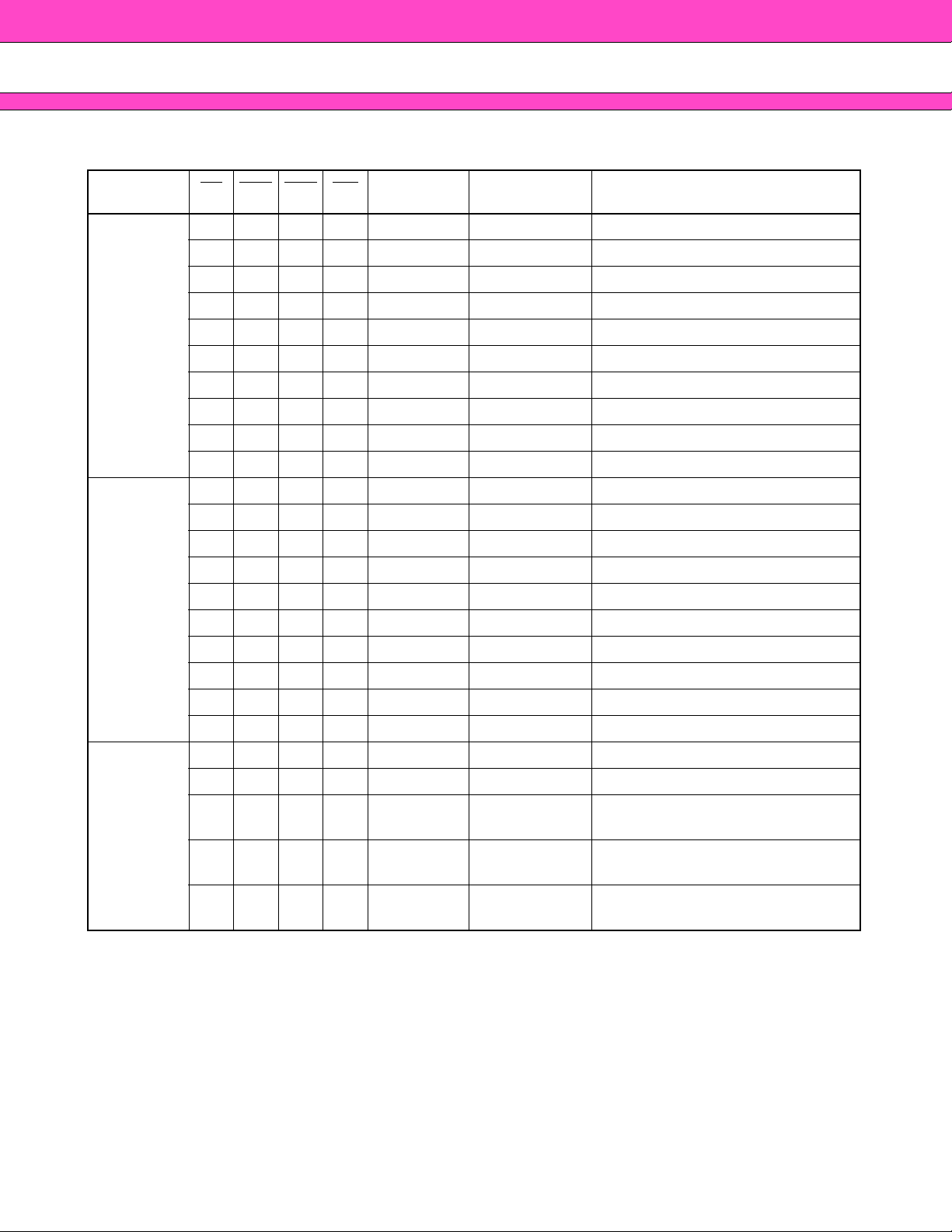
STATE DIAGRAM
■■■■
MINIMUM CLOCK LATENCY OR DELAY TIME FOR SINGLE BANK OPERATION
Second command
(same bank)
First
command
MRS
MRS ACTV READ
l
MRD lMRD lMRD lMRD lMRD lMRD lMRD
READA
WRIT
WRITA
BST
*1
PRE PALL REF SELF
ACTV
READ
READA
WRIT
WRITA
BST
PRE
PALL
lRCD*4lRCD lRCD*4lRCD 1lRAS lRAS
*5, 6
BL/2
+ l
RP
BL/2
+ l
*6
lWAL lWAL
*5, 6
RP
* 4
1
lWRD
*7
lWRD 1
1
*4, 7
11*3lBSNC*3lBSNC 1
lRWD
* 3
*3, 4
lRWD 1
* 4
1
1
BL/2
+ l
RP
lDPL
*4
*4
*4,7
*4
1
BL/2
+ l
RP
lDPL
*4
*4
BL/2
+ l
*4,7
lWAL*4lWAL*6lWAL
*4
1
*4
1
lRP lRP 11*41
*5
lRPA lRPA 111lRPA
lRP
RP
*6
*5, 6
BL/2
+ l
RP
*6
lWAL
*6
*5, 6
lRP
*5
lRPA
REF
SELFX
Notes: *1. BL/2 = t
*2. Assume PALL command does not affect any operation on the other bank(s).
*3. Assume no I/O conflict.
*4. l
RAS must be satisfied.
*5. Assume all outputs are in High-Z state.
*6. Assume all other banks are in idle state.
*7. l
DPL and lWRD are specified from last data input and assumed preceding pair of write data are masked
by DM
Illegal Command
l
RFC lRFC lRFC lRFC lRFC lRFC lRFC
l
XSNR lXSNR lXSNR lXSNR lXSNR lXSNR lXSNR
CK × BL / 2. (Example: In case of BL = 4, BL/2 means 2 clocks.)
0 to DM3 input.
17

MB81P643287-50/-60
MINIMUM CLOCK LATENCY OR DELAY TIME FOR MULTIPLE BANK OPERATION
Second command
(other bank)
First
command
MRS
*8
*10
MRS ACTV
l
MRD lMRD lMRD lMRD lMRD lMRD lMRD
READ
*8
READA
WRIT
*8
WRITA
*8
BST
*9
PRE PALL REF SELF
*2, 9
ACTV
READ
READA
WRIT
WRITA
BST
PRE
PALL
*5, 6
BL/2 +
l
RP
lWAL
*5, 6
lRP
*6
lRRD
*6
111
*6
1
*6
1
*6
*6
1
*6
1
*6
1
*5
*11
1
*11
1
*11
1
* 3
*11
1
*11
11lRAS
lRWD*3lRWD 11*41
*4
1
*7
*4
* 3, 4
1
lRWD
* 3, 4
lRWD 1 BL/2 +
lWRD*7lWRD 11 1
BL/2
+ l
1
1
*4
WRD
*11
*11
*4
BL/2
+ l
WRD
1
*111*3, 11
lBSNC
*111*3, 111*3, 11
*4
*4
1 1lWAL*6lWAL
*3, 11
lBSNC 11*41
*11
1
11*41
l
RP
lDPL
*4,7
lRPA lRPA 111lRPA
BL/2 +
l
RP
lRP
*6
*6
*5, 6
BL/2 +
l
RP
lWAL
*5, 6
lRP
lRPA
*6
*5
18
REF
SELFX
l
RFC lRFC lRFC lRFC lRFC lRFC lRFC
l
XSNR lXSNR lXSNR lXSNR lXSNR lXSNR lXSNR

MB81P643287-50/-60
Notes: *1. BL/2 = t
*2. Assume PALL command does not affect any operation on the other bank(s).
*3. Assume no I/O conflict.
*4. l
RAS must be satisfied.
*5. Assume all outputs are in High-Z state.
*6. Assume the other bank(s) is in idle state.
*7. l
DPL and lWRD are specified from last data input and assumed preceding pair of write data are masked
by DM
*8. Assume the other bank(s) is in active state and l
*9. Assume the other bank(s) is in active state and l
*10. Second command have to follow the minimum clock latency or delay time of single bank operation in
other bank (second command is asserted.)
*11. Assume other banks are not in READA/WRITA state.
Illegal Command.
CK × BL / 2. (Example: In case of BL = 4, BL/2 means 2 clocks.)
0 to DM3 input.
RCD is satisfied.
RAS is satisfied.
19

MB81P643287-50/-60
Fig. 2 - STATE DIAGRAM (Simplified for Single Bank Operation)
MODE
REGISTER
SET
POWER
DOWN
WRIT
PDEX
WRITE
MRS
PDEN
WRIT
WRITA
WRIT
IDLE
ACTV
BANK
ACTIVE
READA
READ
READ
SELF
SELFX
REF
BST
READ
SELF-
REFRESH
AUTO
REFRESH
READ
20
POWER
ON
APPLIED
with PDEN
WRITA
WITH AUTO
PRECHARGE
PDEX and 8 PRE (or 1 PALL)
POWER
WRITE
READA
PRE or
PALL
PRECHARGE
DEFINITION OF ALLOWS
Manual
Input
WRITA
PALL
PRE or
PRE or
PALL
READA
READ WITH
AUTO
PRECHARGE
Automatic
Sequence

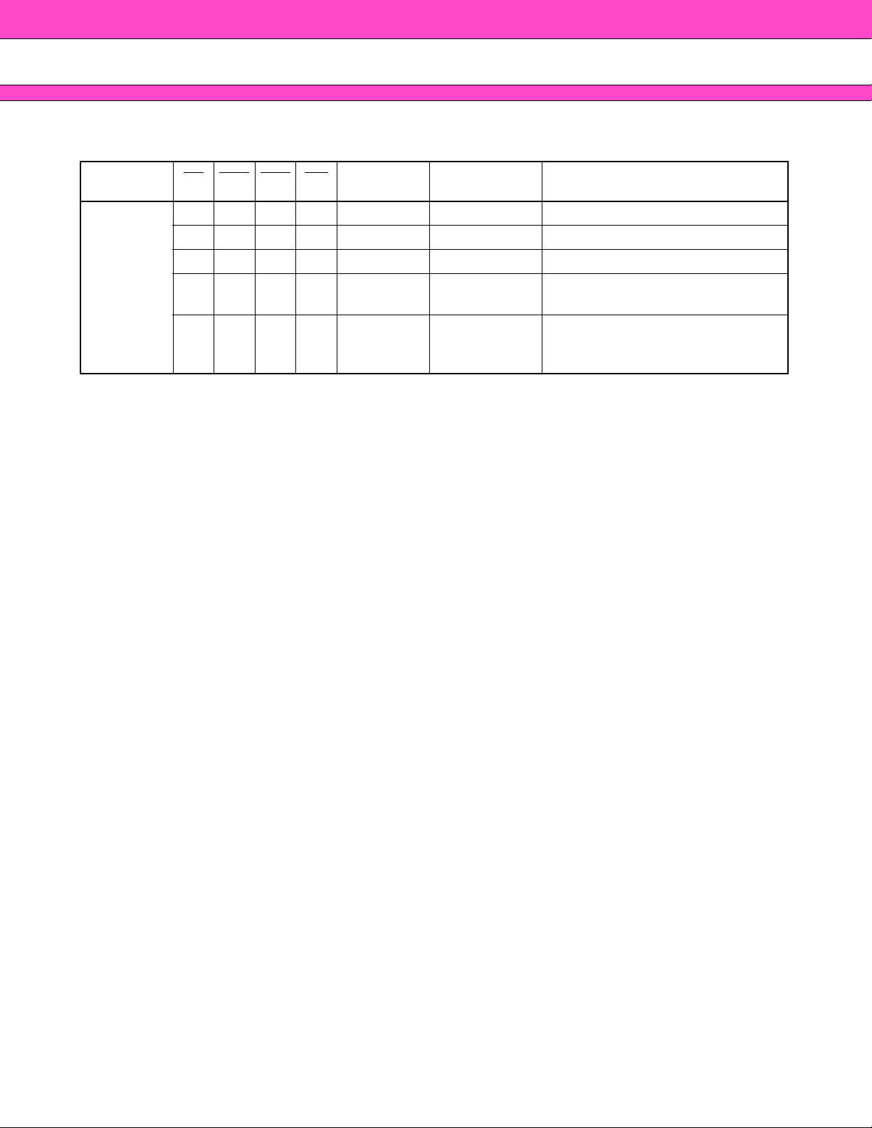
MB81P643287-50/-60
FUNCTIONAL DESCRIPTION
■■■■
DDR, Double Data Rate Function
The regular SDRAM read and write cycle have only used the rising edge of external clock input. When clock
signal goes to High from Low at the read mode, the read out data will be available at every rising clock edge
after the specified latency up to burst length. The MB81P643287 DDR FCRAM features a twice of data tr ansf er
rate within a same clock period by transferring data at every rising and falling clock edge. Refer to Figure 3.
FCRAM
TM
The MB81P643287 utilizes FCRAM core technology. The FCRAM is an acronym of F ast Cycle Random Access
Memory and provides very fast random cycle time, low latency and lo w power consumption than regular DRAMs.
CLOCK INPUT (CLK, CLK
)
The MB81P643287 adopts differential clock scheme. CLK is a master clock and its rising edge is used to latch
all command and address inputs. CLK
is a complementary clock input.
The MB81P643287 implements Delay Lock ed Loop (DLL) circuit. This internal DLL tracks the signal cross point
between CLK and CLK
and generate some clock cycle delay for the output buffer control at Read mode.
The internal DLL circuit requires some Lock-on time for the stable delay time generation. In order to stabilize
the delay, a constant stable clock input f or l
stable clock input f or l
SCD period is also required after Self-refresh exit as specified lSCD prior to the any command.
PCD period is required during the Power-up initialization and a constant
POWER DOWN (CKE)
CKE is a synchronous input signal and enables power down mode.
When all banks are in idle state, CKE controls P ower Down (PD) and Self-refresh mode. The PD and Self-refresh
is entered when CKE is brought to Low and exited when it returns to High.
During the Power Down and Self-refresh mode, both CLK and CLK
are disabled after specified time.
CKE does not have a Cloc k Suspend function unlike CKE pin of regular SDRAMs, and it is illegal to bring CKE
into Low if any read or write operation is being performed. For the detail, refer to Timing Diagrams.
It is recommended to maintain CKE to be Low until V
DD gets in the specified operating range in order to assure
the power-up initialization.
CHIP SELECT (CS
CS
enables all commands inputs, RAS, CAS , and WE, and address input. When CS is High, all command signals
)
are negated but internal operation such as burst cycle will not be suspended.
COMMAND INPUTS (RAS
As well as regular SDRAMs, each combination of RAS
, CAS and WE)
, CAS and WE input in conjunction with CS input at a
rising edge of the CLK determines SDRAM operation. Refer to “■FUNCTION TRUTH TABLE”.
21

MB81P643287-50/-60
BANK ADDRESS (BA
0
to BA
2
)
The MB81P643287 has eight internal banks and each bank is organized as 256K words by 32-bit.
Bank selection by BA occurs at Bank Active command (A CTV) f ollowed by read (READ or READA), write (WRIT
or WRITA), and Precharge(PRE) command.
ADDRESS INPUTS (A
0
to A10)
Address input selects an arbitrary location of a total of 2,097,152 words of each memory cell matrix within each
bank. A total of twenty address input signals are required to decode such a matrix. DDR SDRAM adopts an
address multiplexer in order to reduce the pin count of the address line. At a Bank Active command (ACTV),
eleven Ro w addresses are initially latched as well as three Bank addresses and the remainder of se ven Column
addresses are then latched by a Column address strobe command of either a read command (READ or READ A)
or write command (WRIT or WRITA).
DATA STROBE (DQ S
DQS
0 to DQS3 are bi-directional signal and represent byte 0 to byte 3, respectiv ely . During Read operation, DQS0
0
to DQS3)
to DQS3 provides the read data strobe signal that is intended to use input data strobe signal at the receiver
circuit of the controller(s). It turns Low before first data is coming out and toggle High to Low or Low to High till
end of burst read. Refer to Figure 3 for the timing example.
The CAS Latency is specified to the first Low to High transition of these DQS
During the write operation, DQS
behavior of read data strobe, the first rising edge of DQS
falling edge of DQS
count. Therefore, DQS
Note that DQS
0 to DQS3 signal latches second input data. This sequence shall be continued till end of burst
0 to DQS3 must be provided from controller that drives write data.
0 to DQS3 input signal should not be tristated from High at the end of write mode.
0 to DQS3 are used to latch write data and Data Mask signals. As well as the
0 to DQS3 input latches first input data and following
0 to DQS3 output.
0
DATA INPUTS AND OUTPUTS (DQ
Input data is latched by DQS
command input. Output data is obtained together with DQS
to DQ31)
0 to DQS3 input signal and written into memory at the clock following the write
0 to DQS3 output signals at programmed read CAS
latency.
The polarity of the output data is identical to that of the input. Data is valid after DQS
transitions (t
WRITE DATA MASK (DM
DM
0 to DM3 are active High enable inputs and represent byte 0 to byte 3 respectively. DM0 to DM3 have a data
input mask function, and are also sampled by DQS
During write cycle, DM
QSQ) as specified in Data Valid Time (tDV).
0
to DM3)
0 to DQS3 input signal together with input data.
0 to DM3 provide byte mask function. When DMx = High is latched by a DQS0 to DQS3
0 to DQS3 output signal
signal edge, data input at the same edge of DQS0 to DQS3 is masked.
During read cycle, all DM
Refer to DM
0 to DM3 TRUTH TABLE.
0 to DM3 are inactive and do not have any effect on read operation.
22

MB81P643287-50/-60
BURST MODE OPERATION AND BURST TYPE
The burst mode provides f aster memory access and MB81P643287 read and write operations are b urst oriented.
The burst mode is implemented by k eeping the same Row address and b y automatic strobing Column address
in every single clock edge till progr ammed b urst length(BL). Access time of b urst mode is specified as t
internal column address counter operation is determined by a mode register which defines burst type(BT) and
burst count length(BL) of 2, 4 or 8 bits of boundary . In order to terminate or to mov e from the current b urst mode
to the next stage while the remaining burst count is more than 2, the following combinations will be required.
Current Stage Next Stage Method (Assert the following command)
Burst Read Burst Read Read Command
ACC. The
1st Step
Burst Stop Command (BST)
Burst Read Burst Write
2nd Step Write Command after l
BSNC
Burst Write Burst Write Write Command
1st Step
Data Mask Input
Burst Write Burst Read
2nd Step Read Command after l
WRD from last data input
Burst Read Precharge Precharge Command
1st Step
Data Mask Input
Burst Write Precharge
2nd Step Precharge Command after l
DPL from last data input
The burst type is sequential only. The sequential mode is an incremental decoding scheme within a boundary
address to be determined by count length, it assigns +1 to the previous (or initial) address until reaching the end
of boundary address and then wraps round to the least significant address(= 0). If the first access of column
address is even (0), the next address will be odd (1), or vice-versa.
Burst Length
Starting Column Address
2
A
A1 A
0
Sequential Mode
X X 0 0 – 1
2
X X 1 1 – 0
X 0 0 0 – 1 – 2 – 3
X 0 1 1 – 2 – 3 – 0
4
X 1 0 2 – 3 – 0 – 1
X 1 1 3 – 0 – 1 – 2
0 0 0 0 – 1 – 2 – 3 – 4 – 5 – 6 – 7
0 0 1 1 – 2 – 3 – 4 – 5 – 6 – 7 – 0
0 1 0 2 – 3 – 4 – 5 – 6 – 7 – 0 – 1
0 1 1 3 – 4 – 5 – 6 – 7 – 0 – 1 – 2
8
1 0 0 4 – 5 – 6 – 7 – 0 – 1 – 2 – 3
1 0 1 5 – 6 – 7 – 0 – 1 – 2 – 3 – 4
1 1 0 6 – 7 – 0 – 1 – 2 – 3 – 4 – 5
1 1 1 7 – 0 – 1 – 2 – 3 – 4 – 5 – 6
23

MB81P643287-50/-60
BURST STOP COMMAND (BST)
The Burst Stop command (BST) terminates the burst read operation except f or a case that Auto-precharge option
is asserted. When the BST command is issued during the burst read operation, the all output buffers, DQs and
DQS
0 to DQS3, will turn to High-Z state after some latencies that to be matched with programmed CAS latency
and internal bank state remains active state.
In a case of terminating the burst write operation, the BST command should not be issued at any time during
burst write operation. Refer to previous page for the write interrupt and termination rule.
PRECHARGE AND PRECHARGE OPTION (PRE, PALL)
The DDR SDRAM memory core is the same as conventional DRAMs’, requiring precharge and refresh operations. Precharge rewrites the bit line and to reset the internal Row address line and is ex ecuted by the precharge
operation (PRE or PALL). With the precharge operation, DDR SDRAM will automatically be in standby state
after specified precharge time (l
The precharged bank is selected by combination of AP and bank address (BA) when precharge command is
issued. If AP = High, all banks are precharged regardless of BA (PALL command). If AP = Low, a bank to be
selected by BA is precharged (PRE command).
The auto-precharge enters precharge mode at the end of burst mode of read or write without Precharge command
issue. This auto-precharge is entered by AP = High when a Read (READ) or Write (WRIT) command is issued.
Applying BST is illegal if the Auto-precharge option is used.
Refer to “■FUNCTION TRUTH TABLE”.
RP, lRPA).
AUTO-REFRESH (REF)
Auto-refresh uses the internal refresh address counter. The MB81P643287 Auto-refresh command (REF) automatically generates Bank Active and Precharge command internally. All banks of SDRAM should be precharged prior to the Auto-refresh command. The Auto-refresh command should also be issued within every 8
µs period.
SELF-REFRESH ENTRY (SELF)
Self-refresh function provides automatic refresh by an internal timer as well as Auto-refresh and will continue
the refresh operation until cancelled by SELFX.
The Self-refresh mode is entered by applying an Auto-refresh command in conjunction with CKE = Lo w (SELF).
Once MB81P643287 enters the self-refresh mode, all inputs except f or CKE can be either logic high or low le v el
state and outputs will be in a High-Z state. During Self-refresh mode, CKE = Low should be maintained. SELF
command should only be issued after last read data has been appeared on DQ.
Note: When the burst refresh method is used, a total of 4096 auto-refresh commands within 4 ms must be asserted
prior to the self-refresh mode entry.
SELF-REFRESH EXIT (SELFX)
To exit Self-refresh mode, CKE must bring to High for at least 2 clock cycles together with NOP condition.
Refer to Timing Diagram f or the detail procedure. It is recommended to issue at least one A uto-refresh command
just after the l
WARNING: A stable clock for l
RFC period to avoid the violation of refresh period.
SCD period with a constant duty cycle must be supplied prior to applying any read
command to insure the DLL is locked against the latest device conditions.
Note: When the burst refresh method is used, a total of 4096 auto-refresh commands within 4 ms must be asserted
both before the self-refresh entry and after the self-refresh exit.
24

MB81P643287-50/-60
MODE REGISTER SET (MRS)
The mode register of SDRAM provides a variety of different operations. The register consists of four operation
fields; Burst Length, Burst Type, CAS Latency, and Test Mode Entry (This Test Mode Entry must not be used).
Refer to MODE REGISTER TABLE.
The mode register can be programmed by the Mode Register Set command (MRS). Each field is set by the
address line. Once a mode register is programmed, the contents of the register will be held until re-progr ammed
by another MRS command (or part loses power). MRS command should only be issued on condition that all
banks are in idle state and all DQS are in High-Z. The condition of the mode register is undefined after the powerup stage. It is required to set each field at power-up initialization.
Refer to POWER-UP INITIALIZATION below.
Note: The Extended Mode Register Set command (EMRS) and its DLL Enable function of EMRS field is only used
at power-on sequence.
POWER-UP INITIALIZATION
The MB81P643287 internal condition at and after power-up will be undefined. It is required to follow the f ollowing
Power On Sequence to execute read or write operation.
1. Apply V
signals to be Low state (or at least CKE to be Low state).
2. Apply V
3. Apply VREF and VTT. (VTT is applied to the system).
4. Start clock after all power supplies reached in a specified operating range and maintain stable condition
for a minimum of 200 µs.
5. After the minimum of 200 µs stable power and clock, apply NOP condition and take CKE to be High
state.
6. Issue Precharge All Banks (PALL) command or Precharge Single Bank (PRE) command to every
banks.
7. Issue EMRS to enable DLL, DE = Low.
8. Issue Mode Register Set command (MRS) to reset DLL, DR = High. An additional clock input for l
period is required to lock the DLL.
9. Apply minimum of two Auto-refresh command (REF).*
10. Program the mode register by Mode Register Set command (MRS) with DR = Low.*
DD voltage to all VDD pins before or at the same time as VDDQ pins and attempt to maintain all input
DD voltage to all VDDQ pins before or at the same time as VREF and VTT.
PCD*
2
2
1
*1:The l
PCD depends on operating clock period. The lPCD is counted from “DLL Reset” at step-8 to any command
input at step-10.
*2:The Mode Register Set command (MRS) can be issued before two Auto-refresh cycle.
POWER-DOWN
The MB81P643287 uses multiple power supply v oltage . It is required to follow the reversed sequence of above
Power On Sequence.
1. Take all input signals to be VSS or High-Z.
2. Deapply V
3. Deapply V
DDQ.
DD at the same time as VDDQ.
25

MB81P643287-50/-60
Fig. 3 - SDRAM READ TIMING EXAMPLE (@ CL=2 & BL=2)
<SDRAM>
t0 t2 t3 t4t1
CLK
(external)
Command
DATA
< DDR SDRAM >
CLK
CLK
Command
DQS
READ
Stored by CLK input
Hi-Z
t0 t0.5 t1 t1.5 t2 t2.5 t3 t3.5 t4
READ
Stored by CLK input
Hi-Z
Low
Q1 Q2
Output in every rising CLK edge
DQS signal transition
occurs at the same
time as data bus.
High
26
DATA
Hi-Z
Q1 Q2
Output in every
cross point of clock input

MODE REGISTER TABLE
■■■■
MODE REGISTER SET
ADDRESS BA
REGISTER 0
*1
2
BA1BA0A
*1
0
MB81P643287-50/-60
10
9
8
A
A
*1
0
0 0 DR TE CL BT BL
7
A
A6 to A
4
3
A
A2 to A
0
6
5
A
A
4
A
00X Reserved
010 2
011 3
100 Reserved
101 Reserved
110 Reserved
111 Reserved
7
A
Test Mode Entry (TE)
0 Normal Operation
Test Mode (Used for Supplier Test
1
Mode)
8
A
DLL RESET (DR)
0 Normal Operation
1 RESET DLL
CAS Latency
(CL)
2
A
1
A
Burst Length
0
A
(BL)
0 0 0 Reserved
001 2
010 4
011 8
1 X X Reserved
3
A
Burst Type (BT)
0 Sequential (Wrap round, Binary up)
1Reserved
EXTENDED MODE REGISTER SET (Note *4)
ADDRESS BA
EXTENDED MODE
REGISTER
*1: A combination of BA
*2: A combination of BA
2
BA1BA0A
*2
0
2 = BA1 = BA0 = 0 (Low) selects standard Mode Register.
1 = BA2 = 0 and BA0 = 1 (High) selects Extended Mode Register.
*21*2
0
10
A9A8A7A6A5A4A3A2A1A
*3: These RESERVED field in EMRS must be set as 0.
RESERVED *
0
A
0 DLL Enable
1 DLL Disable
3
DLL Enable (DE)
0
DE
27

MB81P643287-50/-60
ABSOLUTE MAXIMUM RATINGS (See WARNING)
■■■■
Parameter Symbol Value Unit
Voltage of V
Voltage at Any Pin Relative to V
Short Circuit Output Current I
DD Supply Relative to VSS VDD, VDDQ –0.5 to +3.6 V
SS VIN, VOUT –0.5 to +3.6 V
OUT ±50 mA
Power Dissipation PD 2.0 W
Storage Temperature T
STG –55 to +125 °C
WARNING: Semiconductor devices can be permanently damaged by application of stress (voltage, current,
temperature, etc.) in excess of absolute maximum ratings. Do not exceed these ratings.
RECOMMENDED OPERATING CONDITIONS
■■■■
(Referenced to VSS)
Parameter Notes Symbol Min. Typ. Max. Unit
V
DD 2.3 2.5 2.7 V
Supply Voltage
V
DDQ VDD VDD VDD V
V
SS, VSSQ 000V
Input Reference Voltage *1 VREF VDDQ × 0.49 VDDQ × 0.5 VDDQ × 0.51 V
Termination Voltage *2 V
Single Ended SSTL DC Level Input High Voltage *3 V
Single Ended SSTL DC Level Input Low Voltage *3 V
TT VREF - 0.04 VREF VREF + 0.04 V
IH (DC) VREF + 0.25 — VDDQ + 0.1 V
IL (DC) - 0.1 — VREF - 0.25 V
Single Ended SSTL AC Level Input High Voltage *3, *5 VIH (AC) VREF + 0.35 — — V
Single Ended SSTL AC Level Input Low Voltage *3, *5 V
Differential DC Level Input Voltage Range *3 V
IL (AC) ——VREF - 0.35 V
IN (DC) - 0.1 — VDDQ + 0.1 V
Differential DC Level Differential Input Voltage *3 VSWING (DC) 0.5 — VDDQ + 0.2 V
Differential AC Level Differential Input Voltage *3 V
Differential AC Level Input Crosspoint Voltage *3 V
SWING (AC) 0.7 — — V
X (AC) VDDQ/2 - 0.2 VDDQ/2 VDDQ/2 + 0.2 V
Differential Input Signal Offset Voltage *4 VISO (AC) VDDQ/2 - 0.2 VDDQ/2 VDDQ/2 + 0.2 V
Termination Resistor (SSTL I/Os) *2 R
Ambient Temperature T
T —50—Ω
A 0—70
o
Note 5. Note 6.
VDD + 1.0 V
V
IH
IHmin
V
VIL
50% of pulse amplitude
Pulse width < 4 ns
IH
V
V
ILmax
VIL
−1.0 V
Pulse width < 4 ns
50% of pulse amplitude
C
28

MB81P643287-50/-60
Notes: *1. VREF is expected to track variations in the DC level of VDDQ of the transmitting device. Peak-to-Peak
noise level on V
*2. V
TT is used for SSTL_2 bus and is not applied to the device. VTT is expected to be set equal to VREF
and must be track variations in the DC level of VREF.
*3. Applicable when signal(s) is terminated to the V
*4. V
ISO means {VIN(CLK) + VIN(CLK)} / 2. Refer to Differential Input Signal Definition.
*5. Overshoot limit: V
50% of pulse amplitude.
*6. Undershoot limit: V
50%of pulse amplitude.
WARNING: The recommended operating conditions are required in order to ensure the normal operation of the
semiconductor device. All of the device’s electrical characteristics are warranted when the device is
operated within these ranges.
Always use semiconductor devices within their recommended operating condition ranges. Operation
outside these ranges may adversely affect reliability and could result in device failure.
No warranty is made with respect to uses, operating conditions, or combinations not represented on
the data sheet. Users considering application outside the listed conditions are advised to contact their
FUJITSU representatives beforehand.
REF may not exceed ± 2% of the supplied DC va lue.
TT of SSTL_2 bus.
IH (Max.) = VDD + 1.0V for pulse width ≤ 4 ns acceptable, pulse width measured at
IL (Min.) = VSS -1.0V for pulse width ≤ 4 ns acceptable, pulse width measured at
Differential Input Signal Definition
Fig. 4 - Differential Input Signal Offset Voltage (For Clock Input)
CLK
CLK
VSS
IVSWINGI
0 V Differential
V
ISO
V
VSS
CAPACITANCE
■■■■
ISO (Min.)
Parameter Symbol Min. Typ. Max. Unit
VISO (Max.)
VX
VSWING (AC)
(TA = 25°C, f = 1 MHz)
Input Capacitance, Address & Control C
Input Capacitance, CLK & CLK
IN1 2.5 — 3.5 pF
CIN2 2.5 — 3.5 pF
Input Capacitance, DM0 to DM3 CIN3 4.0 — 5.5 pF
I/O Capacitance C
I/O 4.0 — 5.5 pF
29

MB81P643287-50/-60
DC CHARACTERISTICS
■■■■
(At recommended operating conditions unless otherwise noted.) Note *1,*2,*3
Parameter Symbol Condition
Value
Unit
Min. Max.
Output Minimum Source DC Current I
OH(DC)
Output Minimum Sink DC Current IOL(DC)
Input Leakage Current (any input) I
Output Leakage Current I
VDDQ = 2.3V,
V
OH = VDDQ-0.43V
VDDQ = 2.3V,
V
OL = +0.35V
0 V ≤ VIN ≤ VDD;
LI
All other pins not under test = 0 V
0 V ≤ VIN ≤ VDD;
LO
Data out disabled
-15.2 — mA
15.2 — mA
-10 10 µA
-10 10 µA
VREF Current IREF -10 10 µA
Burst Length = 2
t
CK = Min.,
One bank active,
Address change up to 3 times during l
RC (Min.)
0 V ≤ V
V
IN ≤ VIL (Max.),
IH (Min.) ≤ VIN ≤ VDD
—
460
mA
Operating Current
(Average Power
Supply Current)
MB81P643287-50
I
DD1S
MB81P643287-60 405
CKE = VIH, tCK = Min.
MB81P643287-50
All banks idle,
85
NOP commands only,
Standby Current
I
DD2N
Input signals (except to CMD) are
—
mA
changed one time during 20 ns
MB81P643287-60 75
0 V ≤ V
V
IN ≤ VIL (Max.),
IH (Min.) ≤ VIN ≤ VDD
Power Down Current I
MB81P643287-50
Active Standby Current
(Power Supply Current)
MB81P643287-60 225
30
DD2P
I
DD3N
CKE = VIL, tCK = Min.
All banks idle,
0 V ≤ V
IN ≤ VDD
CKE = VIH, tCK = Min.
All banks Active,
NOP commands only,
Input signals (except to CMD) are
changed one time during 20 ns
0 V ≤ V
V
IN ≤ VIL (Max.),
IH (Min.) ≤ VIN ≤ VDD
—35mA
260
—
mA
(Continued)

(Continued)
Parameter Symbol Condition
Burst Read Current
(Average Power
Supply Current)
Burst Write Current
(Average Power
Supply Current)
MB81P643287-50/-60
Value
Min. Max.
Burst Length = 4,
MB81P643287-50
CAS Latency = 3,
All bank active,
I
DD4R
MB81P643287-60 460
Gapless data,
t
CK = Min.,
0 V ≤ V
V
IN ≤ VIL (Max.),
IH (Min.) ≤ VIN ≤ VDD
—
Burst Length = 4,
MB81P643287-50
CAS Latency = 3,
All bank active,
I
DD4W
MB81P643287-60 505
Gapless data,
t
CK = Min.,
0 V ≤ V
V
IN ≤ VIL (Max.),
IH (Min.) ≤ VIN ≤ VDD
—
535
595
Unit
mA
mA
Auto-refresh Current
MB81P643287-50
(Average Power
Supply Current)
MB81P643287-60 270
Self-refresh Current
(Average Power Supply Current)
Notes: *1. All voltages referenced to VSS.
*2. DC characteristics are measured after following the POWER-UP INITIALIZATION procedure.
*3. I
DD depends on the output termination or load conditions, clock cycle rate, and number of address and
command change within certain period. The specified values are obtained with the output open.
I
I
DD5
DD6
Auto-refresh;
t
CK = Min.,
0 V ≤ V
V
IN ≤ VIL (Max.),
IH (Min.) ≤ VIN ≤ VDD
Self-refresh;
CKE = V
0 V ≤ V
IL,
IN ≤ VDD
320
—
mA
—5mA
31

MB81P643287-50/-60
AC CHARACTERISTICS
■■■■
(Recommended operating conditions unless otherwise noted.) Note *1,*2,*3
AC PARAMETERS (CAS LATENCY DEPENDENT)
Parameter Symbol
MB81P643287-50 MB81P643287-60
Min. Max. Min. Max.
Unit
Clock Period t
CK
ns
CL = 2 7.5 10.5 9.0 10.5
MB81P643287-50 MB81P643287-60
CL = 3 5.0 9.0 6.0 10.5
Parameter Notes Symbol
Unit
Min. Max. Min. Max.
Input Setup Time
(Except for DQS, DM and DQs)
Input Hold Time
(Except for DQS, DM and DQs)
DM and Data Input Setup Time *5 t
DM and Data Input Hold Time *5 t
DQS First Input Setup Time
(Input Preamble Setup Time)
Last Data Output to CKE High Level
Hold Time
Input Transition Time *7 t
Precharge Power Down Exit
and Self-refresh Exit Time
*4 t
IS 1.0 — 1.2 — ns
*4 tIH 1.0 — 1.2 — ns
DS 0.6 — 0.7 — ns
DH 0.6 — 0.7 — ns
*6 tDSPRES 0—0—ns
t
QCKEH 0—0—ns
T 0.1 0.8 0.1 0.9 ns
*4 t
PDEX 3.0 — 3.6 — ns
Time between Refresh *8 tREF —32—32ms
Time between Auto-refresh Command *8 t
Pause Time after Power-on t
32
AREF —8.0—8.0µs
PAUSE 200 — 200 — µs

AC PARAMETERS (FREQUENCY DEPENDANT) Note *9
Parameter Notes Symbol Min. Max. Unit
MB81P643287-50/-60
Clock High Time *4 t
Clock Low Time *4 t
DQS Low to High Input Transition
Setup Time from CLK
*4, *10 t
CH 0.45 × tCK —ns
CL 0.45 × tCK —ns
DQSS 0.75 × tCK 1.25 × tCK ns
DQS Low Input Pulse Width tDSL 0.4 × tCK —ns
DQS High Input Pulse Width t
DQS First Low Input Hold Time
(Input Preamble Hold Time)
DQS First Low Input Pulse Width
(Input Preamble Pulse Width)
DQS Last Low Input Hold Time
(Input Postamble Hold Time)
DQS Access Time from Clock *4 t
DSH 0.4 × tCK —ns
*4 t
DSPREH 0.25 × tCK —ns
tDSPRE 0.4 × tCK —ns
t
DSPST 0.4 × tCK —ns
QSCK - 0.1 × tCK - 0.2 0.1 × tCK + 0.2 ns
DQS Output Valid Time tQSV 0.3 × tCK —ns
DQS Output in Low-Z
(Output Preamble Setup Time)
DQS First Low Output Hold Time
(Output Preamble Hold Time)
DQS Last Low Output Hold Time
(Output Postamble Hold Time)
DQS Last Low Output in High-Z
from CLK or CLK
*4, *11 t
*4, *12 t
QSLZ - 0.1 × tCK - 0.2 — ns
*4 t
QSPRE 0.9 × tCK - 0.2 1.1 × tCK + 0.2 ns
QSPST 0.4 × tCK - 0.2 0.6 × tCK + 0.2 ns
*12 tQSHZ — 0.1 × tCK + 0.2 ns
DQ Access Time from CLK & CLK
DQ Access Time from DQS *5 t
*4 tACC - 0.1 × tCK - 0.2 0.1 × tCK + 0.2 ns
QSQ - 0.1 × tCK 0.1 × tCK ns
DQ Output Data Valid Time from DQS tDV 0.3 × tCK —ns
DQ Output in Low-Z *4, *11 t
DQ Output in High-Z *4, *12 t
LZ - 0.1 × tCK - 0.2 — ns
HZ - 0.1 × tCK - 0.2 0.1 × tCK + 0.2 ns
DQ & DM Input Pulse Width tDIPW 0.4 × tCK —ns
DQS Falling Edge to Clock Hold Time t
DQS Falling Edge to Clock Setup Time t
DSCH
DSCS
0.2 × tCK
(1.5 ns Min.)
0.2 × tCK
(1.5 ns Min.)
—ns
—ns
33

MB81P643287-50/-60
CK
EXAMPLE OF FREQUENCY DEPENDANT AC PARAMETERS (@ Minimum t
CK
= 5ns tCK = 6ns tCK = 7.5ns tCK = 9ns tCK = 10.5ns
Parameter Symbol
t
Min. Max. Min. Max. Min. Max. Min. Max. Min. Max.
Clock High Time tCH 2.3—2.7—3.4—4.1—4.8—ns
)
Unit
Clock Low Time t
DQS Low to High Input
Transition Setup Time from CLK
DQS Low Input Pulse Width t
DQS High Input Pulse Width t
DQS First Low Input Hold Time
(Input Preamble Hold Time)
DQS First Low Input Pulse Width
(Input Preamble Pulse Width)
DQS Last Low Input Hold Time
(Postamble Hold Time)
CL 2.3—2.7—3.4—4.1—4.8—ns
tDQSS 3.8 6.3 4.5 7.5 5.7 9.4 6.8 11.3 7.9 13.2 ns
DSL 2.0—2.4—3.0—3.6—4.2—ns
DSH 2.0—2.4—3.0—3.6—4.2—ns
tDSPREH 1.3—1.5—1.9—2.3—2.7—ns
t
DSPRE 2.0—2.4—3.0—3.6—4.2—ns
t
DSPST 2.0—2.4—3.0—3.6—4.2—ns
DQS Access Time from Clock tQSCK -0.7 0.7 -0.8 0.8 -1.0 1.0 -1.1 1.1 -1.3 1.3 ns
DQS Output Valid Time t
DQS Output in Low-Z
(Output Preamble)
DQS First Low Output Hold Time
(Output Preamble)
DQS Last Low Output Hold Time
(Output Postamble)
DQS Last Low Output in High-Z
from CLK or CLK
QSV 1.5—1.8—2.3—2.7—3.2—ns
t
QSLZ -0.7 — -0.8 — -1.0 — -1.1 — -1.3 — ns
tQSPRE 4.3 5.7 5.2 6.8 6.6 8.5 7.9 10.1 9.3 11.8 ns
t
QSPST 1.8 3.2 2.2 3.8 2.8 4.7 3.4 5.6 4.0 6.5 ns
tQSHZ —0.7—0.8—1.0—1.1—1.3ns
DQ Output Access Time
from CLK & CLK
DQ Output Access Time
from DQS
DQ Output Data Valid Time
from DQS
DQ Output in Low-Z t
tACC -0.7 0.7 -0.8 0.8 -1.0 1.0 -1.1 1.1 -1.3 1.3 ns
tQSQ -0.5 0.5 -0.6 0.6 -0.8 0.8 -0.9 0.9 -1.1 1.1 ns
t
DV 1.5—1.8—2.3—2.7—3.2—ns
LZ -0.7 — -0.8 — -1.0 — -1.1 — -1.3 — ns
DQ Output in High-Z tHZ -0.7 0.7 -0.8 0.8 -1.0 1.0 -1.1 1.1 -1.3 1.3 ns
DQ & DM Input Pulse Width t
DQS Falling Edge to Clock Hold
Time
DQS Falling Edge to Clock
Setup Time
DIPW 2.0—2.4—3.0—3.6—4.2—ns
t
DSCH 1.5—1.5—1.5—1.8—2.1—ns
tDSCS 1.5—1.5—1.5—1.8—2.1—ns
34

MB81P643287-50/-60
LATENCY
(The latency values on these parameters are fixed regardless of clock period.)
Parameter Notes
Symbol
MB81P643287-50 MB81P643287-60
Min. Max. Min. Max.
Unit
RAS
Cycle Time *13
RAS Active Time
RAS Precharge Time lRP 2—2—tCK
RAS to CAS Delay Time
RAS to RAS Bank Active Delay Time lRRD 1—1—tCK
Precharge All Bank to Active
Read Command to Write
Command Delay
Last Input Data to Read Command *14
Delay
Last Input Data to Precharge Command
Lead Time *14
Write with Auto Precharge Command to
Active command Delay *14
Mode Register Access to Next Command
Input Delay
CL = 3
lRC
CL = 2 5 — 5 — tCK
CL = 3
lRAS
CL = 2 3 7333 3 7333 tCK
CL = 3
lRCD
CL = 2 2 — 2 — tCK
CL = 3
lRPA
CL = 2 3 — 3 — tCK
CL = 3
lRWD
CL = 2 BL/2+2 — BL/2+2 — tCK
lWRD 2.5 — 2.5 — tCK
lDPL 2.5 — 2.5 — tCK
lWAL BL/2+3+lRP — BL/2+3+lRP —tCK
lMRD 2—2—tCK
6—6—tCK
4 11000 4 11000 tCK
3—3—tCK
4—4—tCK
BL/2+3 — BL/2+3 — tCK
CAS to CAS Delay lCCD 1—1—tCK
CAS Bank Delay lCBD 1—1—tCK
Precharge Power Down Exit to Next
Command Input Delay
Minimum Stable Clock Input After Self- *15
refresh Exit Before READ Command Input
Minimum Stable Clock Input After Self-
refresh Exit Before non-READ Command
Input
Minimum Stable Clock Input for
DLL Lock-on in Power-up
Initialization sequence. *16
Auto-refresh Cycle Time lRFC 12 — 12 — tCK
tCK ≤ 7.5ns
tCK ≤ 10.5ns 630 — 630 — tCK
lPDEXP 2—2—tCK
lSCD 400—400—tCK
l
XSNR 12 — 12 — tCK
400—400—tCK
l
PCD
35

MB81P643287-50/-60
LATENCY - FIXED VALUES
(The latency values on these parameters are fixed regardless of clock period.)
Parameter Notes Symbol MB81P643287-50 MB81P643287-60 Unit
BST Command to Output in High-Z
BST Command to New Command Input *17
DM to Input Data Delay lDQD 00tCK
Precharge to Output in High-Z
CKE Low to Command/Address Input Inactive lCKE 11tCK
CL = 3
CL = 2 2 2 tCK
CL = 3
CL = 2 2 2 tCK
CL = 3
CL = 2 2 2 tCK
l
BSH
lBSNC
lROH
33tCK
33tCK
33tCK
36

MB81P643287-50/-60
Notes: *1. AC characteristics are measured after f ollowing the POWER-UP INITIALIZATION procedure and stab le
clock input with constant clock period and with 50% duty cycle.
*2. Access Times assume input slew rate of 1ns/volt between V
V
DDQ/2, with SSTL_2 output load conditions. Refer to AC TEST LOAD CIRCUIT.
*3. V
REF = 1.25V is a typical reference level for measuring timing of input signals.
Transition times are measured between V
IH(Min.) and VIL(Max.) unless otherwise noted.
Refer to AC TEST CONDITIONS.
*4. This parameter is measured from the cross point of CLK and CLK
*5. This parameter is measured from signal transition point of DQS
*6. The specific requirement is that DQS be valid (HIGH or LOW) on or before this CLK edge. The case
shown (DQS going from High-Z to logic LOW) applies when no writes were previously in progress on
the bus. If a previous write was in progress, DQS could be HIGH at this time, depending on t
*7. t
T is defined as the transition time between VIH (AC)(Min.) and VIL (AC)(Max.).
*8. Total of 4096 REF command must be issued within t
REF (Max.). tAREF is a reference value f or distrib uted
refresh and specifies the time between one REF command to next REF command e xcept for a condition
where CKE = Low during Self-refresh mode.
*9. This parameter is scalable by actual clock period (t
jitters on clock input, T
A and level of VDD and VDDQ.The internal DLL circuit can adjust delay time against
CK) and affected by an abrupt change of duty cycle,
the change of following condition :
T
A < 0.1 °C / 20 ns,
V
DD < 1 mV / 10 ns,
V
DDQ < 1 mV / 10 ns,
if change rate is bigger than these values, frequency dependent A C par ameters aff ected b y DLL jitters.
*10. More than 2 signal edge of DQS
0 to DQS3 should not be input within 1 clock (tCK) cycle.
*11. Low-Z (Low Impedance State) is specified and measured at V
*12. t
QSPST, tQSHZ and tHZ are specified where output buffer is no longer driven.
*13. Actual clock count of l
*14. Assume t
DQSS = 1 × tCK. If actual tDQSS is within specified minimum and maximum range, those par ameters
can be assumed t
RC will be sum of clock count of lRAS and lRP.
DQSS = 1 × tCK.
*15. Applicable also if device oper ating conditions such as supply voltages , case temperature , and/or cloc k
frequency (t
*16. Clock period must satisfy specified t
CK difference must be 0.2 ns or less) is changed during any operation.
CK and it must be stable.
*17. Assume BST is effective to read operation (issued prior to the end of burst read).
REF+0.35V to VREF-0.35V, where VREF is
input.
0 to DQS3 input crossing VREF level.
DSS.
TT ± 200mV.
37

MB81P643287-50/-60
Fig. 5 - AC TEST LOAD CIRCUIT (SSTL_2, Class II)
Output
measurement
point
RS = 25 Ω
Output
VDDQ
0.5 × V
DDQ
Device
Under
Test
V
DDQ
VREF
Z0 = 50 Ω
TT = 0.5 × VDDQVTT = 0.5 × VDDQ
V
RT2 = 50 ΩRT1 = 50 Ω
VREF = 0.5 × VDDQ
CL = 20 pF
V
SS
Note: AC characteristics are measured in this condition. This load circuit is not applicable f or DC Test.
AC TEST CONDITIONS
Parameters Symbol Value Unit
Single-end Input
Input High Level V
Input Low Level V
IH VREF + 0.35 V
IL VREF − 0.35 V
Input Reference Level VREF VDDQ / 2 V
Input Slew Rate SLEW 1.0 V/ns
Differential Input (CLK and CLK
)
Input Reference Level Vr VX (AC)*V
Input Level V
SWING 0.7 V
Input Slew Rate SLEW 1.0 V/ns
38
* : V
X means the actual cross point between CLK and CLK input.

MB81P643287-50/-60
Fig. 6 - AC TIMING of CLK & CLK
tCK tCL tCH
CLK
CLK
Note: Reference level for AC timings of clock are the cross point of CLK and CLK as specified in VX.
Fig. 7 - AC TIMING of Command Input & Address
tCK
CLK
CLK
VX
VSWING (AC)
VX
tIS tIH
Input
(Controls &
Addresses)
Input Valid
VREF
VIH (AC)
VIL (AC)
Note: The cross point of CLK and CLK (VX) is used for command and address input.
The reference level of single ended input is V
REF.
Fig. 8 - AC TIMING of Write Mode (Data Strobe, Write Data and Data Mask Input)
CLK
CLK
Input
(Controls &
Addresses)
DQS Input
(@BL = 4)
VREF
tIS tIH
Write Command
tDSPRES
VIL
tDQSS
tCK
VREF
tDSPREH
tDSPRE
VIH (AC)
VIL (AC)
tDSH tDSL tDSH tDSPST
tDSCH
tDS tDH
tCK
tDSCS
tDQSS
tDS tDH tDS tDH tDS tDH
VREF
Input
(Data & DM)
Input Valid Input Valid Input Valid Input Valid
tDIPW tDIPW tDIPW tDIPW
39

MB81P643287-50/-60
Fig. 9 - AC TIMING of Read Mode (Clock to DQS Output Delay Time)
tCK
tCK
CLK
CLK
DQS Output
(@BL = 4)
TT
V
tQSLZ
(Min.)
VTT − 0.2 V
tQSCK(Min.)
tQSPRE
tQSCK
(Min.)
tQSCK
(Max.)
tQSV
tQSCK
(Min.)
tQSCK
(Max.)
tQSV
Note: DQS Access time (tQSCK) is measured from the cross point of clock (VX) and VREF.
The end of t
QSPST and tQSHZ specification is defined at where output buffer is no longer driven.
Fig. 10 - AC TIMING of Read Mode (Clock to Data Output Delay Time)
CLK
CLK
DQS Data
Output
(@BL = 4)
tCK
tLZ
(Min.)
TT
V
VTT + 0.2 V
VTT − 0.2 V
tACC
(Min.)
tACC
(Max.)
tCK
tACC
(Min.)
tACC
(Max.)
tQSCK
(Min.)
tQSCK
(Max.)
tQSV
tACC
(Min.)
tACC
(Max.)
tQSHZ
tQSCK
(Max.)
tQSPST
tACC
(Max.)
VX
VX
tHZ
40
Note: Access time (tACC) is measured from the cross point of clock (VX) and VREF.
The end of t
HZ specification is defined at where output buffer is no longer driven.
Fig. 11 - AC TIMING of Read Mode (DQS Output to Data Output Delay Time)
DQS Output
(@BL = 4)
DQ Data
Output
(@BL = 4)
tQSQ
(Min.)
TT
V
TT + 0.2 V
V
VTT − 0.2 V
tQSQ
(Min.)
tQSQ
(Max.)
tDV
tQSQ
(Min.)
tQSQ
(Max.)
tDV tDV tDV
Note: DQS Output Edge to Data Output Edge Skew Time (tQSQ) is measured from VTT to VTT.
tQSQ
(Min.)
tQSQ
(Max.)
VREF
tQSQ
(Max.)

MB81P643287-50/-60
Fig. 12 - AC TIMING, PULSE WIDTH
CLK
CLK
VX
IRAS, IRP, IRPA, IRCD, IRRD, tREF, tAREF
Input
(Controls &
Command Command
Addresses)
Note: All parameters listed above are measured from the cross point at rising edge of the CLK and
falling edge of CLK
of one command input to next command input.
Fig. 13 - AC TIMING of Precharge Power Down Mode
IRC (Min.), tREF (Max.)
X
V
CKE
REF
V
tIS
t
PDEX
CLK
CLK
Command
ICKE
NOP NOP NOP ACTVDon't CareNOP NOP
Note*1
Notes: *1. Minimum 2 clock cycles is required for complete power down on clock buffer.
*2. If either any supply voltage or cloc k input condition is changed from the previous operating
condition (other than PDEN and REF), l
SCD must be satisfied prior to any command input.
Fig. 14 - AC TIMING of Self-refresh Mode
2
tPDEXtIS
CKE
CLK
IRFC (Min.) *
VREF
PDEXP (Min.) *2
I
3
SCD *
or IXSNR
I
CLK
1
Note *
Command
ICKE
NOP NOP NOP ACTVDon't CareSELF NOP
Notes: *1. Minimum 2 clock cycles is required for complete power down on clock buffer.
*2. CKE must maintain High lev el and cloc k m ust be pro vided during the l
SCD period. lSCD must
be satisfied before read command input.
*3. l
SCD must be satisfied before read command input.
41

MB81P643287-50/-60
TIMING DIAGRAMS
■■■■
TIMING DIAGRAM - 1: COLUMN ADDRESS TO COLUMN ADDRESS INPUT DELAY
CLK
CLK
lRCD (Min.) lCCD (Min.) lCCD lCCD lCCD
Address
Row
Address
Column
Address
Column
Address
Column
Address
RAS
CAS
Note: lCCD, CAS to CAS address delay, is applicable to the same bank access and
it can be one or more clock period.
TIMING DIAGRAM - 2: DIFFERENT BANK ADDRESS INPUT DELAY
CLK
CLK
lRRD (Min.)
lCBD (Min.) lCBD lCBD lCBD
Column
Address
Column
Address
42
Address
BA
0, BA1
RAS
CAS
Row
Address
Bank 0
lRCD (Min.)
Row
Address
Bank 1 Bank 0 Bank 1 Bank 2 bank 3
Column
Address
lRCD (Min.)
Column
Address
Column
Address
Column
Address

MB81P643287-50/-60
TIMING DIAGRAM - 3: READ (EXAMPLE @ BL = 4)
CLK
CLK
CKE
Command
DQS
(Output)
@CL = 2
DQ
0 to DQ31
(Output)
@CL = 2
DQS
(Output)
@CL = 3
DQ
0 to DQ31
(Output)
@CL = 3
High
Hi-Z
Hi-Z
Hi-Z
Hi-Z
ICCD (Min.)
READ READ NOP
CAS Latency
CAS Latency
Preamble
Q1 Q2 Q1 Q2 Q3 Q4
CAS Latency
CAS Latency
Preamble
Q1 Q2 Q1 Q2 Q3 Q4
Note: CAS Latency is defined from Read command to first rising edge of DQS
Preamble is 1 × t
CK length and starts driving Low level.
0 to DQS3 output.
43

MB81P643287-50/-60
TIMING DIAGRAM - 4: WRITE (EXAMPLE @ BL = 4)
CLK
CLK
CKE
Command
DQS (Input)
DQ
0 to DQ31
(Input)
High
Don't Care
Don't Care
ICCD (Min.)
WRIT WRIT NOP Don't Care
tDSPRES tDSPREH
tDSPRE
tDQSS
tDQSS
Don't Care
D1 D2 D1 D2 D3 D4
Note: DQS Setup Time, tDQSS, must be within a r ange of 0.75*tCK to 1.25*tCK from write command Input.
TIMING DIAGRAM - 5: DM, WRITE DATA MASK (EXAMPLE @ BL = 4)
CLK
44
CLK
Command
DQS (Input)
DM
DQ
0 to DQ31
(Input)
Don't Care
Don't Care
Don't Care
WRIT NOP WRIT
tDQSS tDQSS
D1 D2 D4 D1 D3 D4
Masked Masked
NOP
lDQD = 0 lDQD = 0
Note: DM are latched by DQS Input together with Data Input after write command.
Don't Care
Don't Care
Don't Care

MB81P643287-50/-60
TIMING DIAGRAM - 6: READ WITH AUTO-PRECHARGE
(EXAMPLE @ CL = 2.0, BL = 4 Applied to same bank)
CLK
CLK
Command
DQS (Output)
DQ
0 to DQ31
(Output)
IRAS (Min.)
ACTV READA ACTV
IRCD (Min.)
Hi-Z
Hi-Z
CAS Latency
BL
× tCK + lRP (See note)
2
Q1 Q2 Q3 Q4
IRP (Min.)
Note: Internal precharge operation at Read with Auto-precharge command (READA) is started BL/2
clock later from READA command.
If BL=2, the READA command should not be issued no earlier than 1 clock (BL/2 = 1) before
l
RAS (Min.).
If BL=4, the READA command should not be issued no earlier than 2 clock (BL/2=2) bef ore l
(Min.).
RAS
TIMING DIAGRAM - 7: WRITE WITH AUTO-PRECHARGE
(EXAMPLE @ CL = 2.0, BL = 4 Applied to same bank)
CLK
CLK
Command
DQS (Input)
DQ
0 to DQ31
(Input)
IRAS (Min.) (See note)
ACTV WRITA ACTV
IRCD (Min.)
Hi-Z
Hi-Z
tDQSS
D1 D2 D3 D4
IWAL (Min.)
Note: Write with Auto-precharge command (WRITA) must be issued after l
considered to meet l
RAS requirement applied to end of burst length (BL) regardless of where it is
masked or not.
RCD is satisfied and be
45

MB81P643287-50/-60
TIMING DIAGRAM - 8: READ INTERRUPTED BY PRECHARGE
(EXAMPLE @ CL = 2, BL = 8)
CLK
CLK
Command
DQS (Output)
DQ0 to DQ31
(Output)
Command
DQS (Output)
DQ
0 to DQ31
(Output)
Command
DQS (Output)
READ
Hi-Z
Hi-Z
READ NOP PRE NOP
Hi-Z
Hi-Z
READ NOP PRE NOP
Hi-Z
PRE
IROH ( = CAS Latency)
NOP
Q1 Q2
IROH ( = CAS Latency)
Q1 Q2 Q3 Q4
IROH ( = CAS Latency)
46
DQ
0 to DQ31
(Output)
Command
DQS (Output)
DQ
0 to DQ31
(Output)
Hi-Z
READ NOP PRE NOP
Hi-Z
Hi-Z
Q1 Q2 Q3 Q4 Q5 Q6
No effect (End of Burst)
Q1 Q2 Q3 Q4 Q5 Q6 Q7 Q8
Note: lROH is the same as CAS Latency (CL). In case of CL =3, the lROH is 3 clock.

MB81P643287-50/-60
TIMING DIAGRAM - 9: READ INTERRUPTED BY BURST STOP
(EXAMPLE @ CL = 2, BL = 8)
CLK
CLK
Command
DQS (Output)
DQ0 to DQ31
(Output)
Command
DQS (Output)
DQ
0 to DQ31
(Output)
Command
DQS (Output)
READ
Hi-Z
Hi-Z
READ NOP BST NOP
Hi-Z
Hi-Z
READ NOP BST NOP
Hi-Z
BST
IBSH ( = CAS Latency)
NOP
Q1 Q2
IBSH ( = CAS Latency)
Q1 Q2 Q3 Q4
IBSH ( = CAS Latency)
DQ
0 to DQ31
(Output)
Command
DQS (Output)
DQ
0 to DQ31
(Output)
Hi-Z
READ NOP BST NOP
Hi-Z
Hi-Z
Q1 Q2 Q3 Q4 Q5 Q6
No effect (End of Burst)
Q1 Q2 Q3 Q4 Q5 Q6 Q7 Q8
Note: lBSH is the same as CAS Latency (CL). In case of CL =3, the lBSH is 3 clock.
47

MB81P643287-50/-60
TIMING DIAGRAM - 10: WRITE INTERRUPTED BY PRECHARGE (EXAMPLE @ CL = 2, BL = 8)
CLK
CLK
IRP (Min.)
Command
DQS (Iutput)
DM
DQ
0 to DQ31
Don't Care
Don't Care
Don't Care
WRIT
NOP PRE NOP ACTV
IDPL(Min.)tDQSS
D1 D2
(Input)
See Note 2.
Note: 1. DQS Input are not required from when Precharge command is issued.
2. This pair of write data must be masked prior to Precharge command.
TIMING DIAGRAM - 11: READ TO WRITE (EXAMPLE @ CL = 2, BL = 4)
CLK
CLK
IRWD (Min.)
Don't Care
See Note 1.
Don't Care
Don't Care
48
Command
DQS
DM
DQ
0 to DQ31
Hi-Z
Hi-Z
READ
NOP WRIT
CL tDQSS
Don't Care
Q1 D1 D2 D3 D4Q2 Q3 Q4
NOP
I/O open for bus turn-around
Note: lRWD defines a minimum delay from Read to Write command input applied to the same bank.

MB81P643287-50/-60
TIMING DIAGRAM - 12: READ TO WRITE (EXAMPLE @ CL = 2, BL = 4)
CLK
CLK
lBSNC
Command
DQS
DM
DQ
0 to DQ31
READ BST
Hi-Z
Don't Care
Hi-Z
NOP WRIT
lBSH tDQSS
Q1 D1 D2 D3 D4Q2
Terminated
Note: DM are latched by DQS Input after Write command together with data Input.
TIMING DIAGRAM - 13: WRITE TO READ (EXAMPLE @ CL = 2, BL = 8)
CLK
CLK
NOP
Command
DQS
DM
DQ
0 to DQ31
Hi-Z
WRIT
NOP
WRDtDQSS CL
l
D1 D2 Q1 Q2
Terminated by ReadMasked
READ NOP
Don't Care
Hi-Z
Note: Read command must be issued after lWRD is satisfied and proceeding pair of data must be masked.
49

MB81P643287-50/-60
TIMING DIAGRAM - 14: READ WITH AUTO-PRECHARGE
(EXAMPLE @ CL = 2, BL = 4, Multiple Bank Operation)
CLK
CLK
Command
BA0, BA1
DQS (Output)
DQ
0 to DQ31
Hi-Z
Hi-Z
PREREADA READA
lCBD lCBD
Bank 1Bank 0 Bank 2
CAS Latency
Q1 Q3 Q4 Q1 Q2 Q1 Q2 Q3 Q4Q2
BL
× tCK + lRP
lRP (Min.)
2
READA ACTV
lCBD lCBD lCBDlRRD (Min.)
Bank 3 Bank 1
lRCD (Min.)
ACTV READ
Bank 0 Bank 1
(Output)
Note: Back to back Read with A uto-precharge (READ A) command to the diff erent bank in active state
is possible. However, an y new command to the same bank applied READA command can only
be issued after (BL/2) × t
CK+lRP.
TIMING DIAGRAM - 15: WRITE WITH AUTO-PRECHARGE
(EXAMPLE @ CL = 2, BL = 4, Multiple Bank Operation)
50
CLK
CLK
Command
BA0, BA1
WRITAWRITA PRE
lCBD (Min.)
Bank 1Bank 0 Bank 2
tDQSS
lWAL (Min.)
WRITA ACTV
lCBD (Min.)lCBD (Min.)
Bank 3 Bank 2 Bank 0
tDQSS
lRP (Min.)
ACTV
lRRD (Min.)
tDQSS
DQS (Input)
DQ
0 to DQ31
(Input)
D1 D1 D2 D3 D4 D1 D2 D3 D4D2
Note: Back to back Write with A uto-precharge (WRITA) command to the different bank in active state
is possible. However, an y new command to the same bank applied WRITA command can only
be issued after l
WAL.

MB81P643287-50/-60
TIMING DIAGRAM - 16: AUTO-REFRESH ENTRY AND EXIT
CLK
CLK
IRFC (Min.)
Command
REF
NOP Any
TIMING DIAGRAM - 17: SELF-REFRESH ENTRY AND EXIT
IRFC (Min.)
CKE
t
QCKEH tIS tPDEX IXSNR or ISCD *
CLK
CLK
Command
DQS (Output)
DQ
0 to DQ31
(Output)
Q
NOP
Hi-Z
Hi-Z
SELF
Last Data Output
Don't Care
Note * :CKE must maintain High level and stable clock must be provided during the l
After Self-refresh exit, l
XSNR must be satisfied for at least specified period before any command
(except for read) input.
ACTVNOPNOP
SCD period.
TIMING DIAGRAM - 18: MODE REGISTER SET
CLK
CLK
IMRD
Command
NOP
MRS
NOP
Any
Note: MRS command must be issued after the last data is appeared on each DQ.
51

MB81P643287-50/-60
SCITT TEST MODE
■■■■
ABOUT SCITT
SCITT (Static Component Interconnection Test Technology) is an XNOR circuit based test technology that is
used for testing interconnection between SDRAM and SDRAM controller on the printed circuit boards. SCITT
provides inexpensiv e board level test mode in combination with boundary-scan. The basic idea is simple, consider
all output of SDRAM as output of XNOR circuit and each output pin has a unique mapping on the input of
SDRAM. The ideal schematic block diagram is as shown below.
TEST
Control
µC
SDRAM
Boundary
Scan
xAddress
Bus
XNOR
CORE
ASIC
SDRAM Controller
Data Bus
TEST Control : CAS, CS, CKE
xAddress Bus : A
0 to A10, BA0 to BA2, RAS, DM0 to DM3, CLK, CLK, WE
Data Bus : DQ0 to DQ31, DQS0 to DQS3
It is static and provides easy test pattern that result in a high diagnostic resolution for detecting all open/short
faults.
52

MB81P643287-50/-60
SCITT TEST SEQUENCE
The followings are the SCITT test sequence. SCITT Test can be executed after power-on and prior to Precharge
command in“■ FUNCTION DESCRIPTION POWER-UP INITIALIZATION”. Once Precharge command is issued
to SDRAM, it never get back to SCITT Test Mode during regular operation unless reset power supply for the
purpose of a fail-safe way in get in and out of test mode.
1. Maintain all input signals (except CLK,CLK
CLK and CLK
to be complementary state.
2. Apply VDD voltage to all VDD pins before or at the same time as VDDQ pins.
3. Apply V
4. Apply V
DD voltage to all VDDQ pins before or at the same time as VREF and VTT.
REF and VTT (VTT is applied to the system).
5. Maintain stable power for a minimum of 100µs.
6. Enter SCITT test mode.
7. Execute SCITT test.
8. Exit from SCITT mode.
It is required to follow Power On Sequence to execute read or write operation.
9. Start clock after all power supplies reached in a specified operating range and maintain stable condition
for a minimum of 200µs.
10. After the minimum of 200µs stable power and clock, apply NOP condition and take CKE to be High
state.
11. Issue Precharge All Banks (PALL) command or Precharge Single Bank (PRE) command to every
banks.
12. Issue EMRS to enable DLL, DE = Low.
13. Issue Mode Register Set command (MRS) to reset DLL, DR = High. An additional clock input for l
period is required to lock the DLL.
14. Apply minimum of two Auto-refresh command (REF).*
15. Program the mode register by Mode Register Set command (MRS) with DR = Low.*
The 6,7,8 steps define the SCITT mode available. It is possible to skip these steps if necessary (Refer to “■ FUNCTION DESCRIPTION POWER-UP INITIALIZATION”).
) to be Low state (or at least CKE to be Low) and maintain
PCD*
2
2
1
Notes: *1. The l
command input at step-15.
*2. The Mode Register Set command (MRS) can be issued before two Auto-refresh cycle.
PCD depends on operating clock period. The lPCD is counted from “DLL Reset” at step-13 to any
53

MB81P643287-50/-60
COMMAND TRUTH TABLE Note *1
Control Input Output
0
DM
10
,
to
2
DM
3
CAS
CS CKE WE RAS
A
BA
0
to A
0
to BA
SCITT mode entry H→L *2LL X X X X
SCITT mode exit L→H *
SCITT mode
output enable *
4
LLHVV V VVVVV
3
H *5L
*5
XX X XXXXX
Notes: *1. L = Logic Low, H = Logic High, V = Valid, X = either L or H
*2. The SCITT mode entry command assumes the first CAS
falling edge with CS = CKE = L and CLK,CLK
signals are complementary after power on.
*3. The SCITT mode exit command assumes the first CAS
rising edge after the test mode entry.
*4. Refer the test code table.
*5. CS
= H or CKE = L is necessary to disable outputs in SCITT mode exit.
CLK CLK
HL
LH
DQ
to
DQ
0
31
DQS
to
DQS
0
3
XX
54

MB81P643287-50/-60
TEST CODE TABLE
DQ
0 to DQ31 and DQS0 to DQS3 output data is static and is determined by following logic during the SCITT mode
operation.
DQ0 = RAS xnor A0
DQ1 = RAS xnor A1
DQ2 = RAS xnor A2
DQ3 = RAS xnor A3
DQ4 = RAS xnor A4
DQ5 = RAS xnor A5
DQ6 = RAS xnor A6
DQ7 = RAS xnor A7
DQ8 = RAS xnor A8
DQ9 = RAS xnor A9
DQ10 = RAS xnor A10
DQ11 = RAS xnor BA1
DQ12 = RAS xnor BA0
DQ13 = RAS xnor BA2
DQ14 = RAS xnor DM0
DQ15 = RAS xnor DM1
DQ16 = RAS xnor DM2
DQ17 = RAS xnor DM3
DQ18 = RAS xnor CLK
DQ19 = RAS xnor CLK
DQ20 = RAS xnor WE
DQ21 = A0 xnor A1
DQ22 = A0 xnor A2
DQ23 = A0 xnor A3
• EXAMPLE OF TEST CODE TABLE
Input bus Output bus
RAS
A0A1A2A3A4A5A6A7A8A9
0000000000000000000000
1000000000000000000000
0100000000000000000000
0010000000000000000000
0001000000000000000000
0000100000000000000000
0000010000000000000000
0000001000000000000000
0000000100000000000000
0000000010000000000000
0000000001000000000000
0000000000100000000000
0000000000010000000000
0000000000001000000000
0000000000000100000000
0000000000000010000000
0000000000000001000000
0000000000000000100000
0000000000000000010000
0000000000000000001000
0000000000000000000100
0000000000000000000010
0000000000000000000001
0111111111111111111111
1011111111111111111111
1101111111111111111111
1110111111111111111111
1111011111111111111111
1111101111111111111111
1111110111111111111111
1111111011111111111111
1111111101111111111111
1111111110111111111111
1111111111011111111111
1111111111101111111111
1111111111110111111111
1111111111111011111111
1111111111111101111111
1111111111111110111111
1111111111111111011111
1111111111111111101111
1111111111111111110111
1111111111111111111011
1111111111111111111101
1111111111111111111110
1111111111111111111111
A10
BA0
BA1
BA2
DM0
DM1
DM2
DM3
CLK
CLKWEDQ0DQ1
0 = input Low, 1 = input High, L = output Low, H = output High
DQ24 = A0 xnor A4
DQ25 = A0 xnor A5
DQ26 = A0 xnor A6
DQ27 = A0 xnor A7
DQ28 = A0 xnor A8
DQ29 = A0 xnor A9
DQ30 = A0 xnor A10
DQ31 = A0 xnor BA0
DQS0 = A0 xnor BA1
DQS1 = A0 xnor BA2
DQS2 = A0 xnor DM0
DQS3 = A0 xnor DM1
DQ2
DQ3
DQ4
DQ5
DQ6
DQ7
DQ8
DQ9
DQ10
DQ11
DQ12
DQ13
DQ14
DQ15
DQ16
DQ17
DQ18
DQ19
DQ20
DQ21
DQ22
DQ23
DQ24
DQ25
DQ26
DQ27
DQ28
DQ29
DQ30
DQ31
DQS0
DQS1
HHHHHHHHHHHHHHHHHHHHHHHHHHHHHHHHHHHH
LLLLLLLLLLLLLLLLLLLLLHHHHHHHHHHHHHHH
LHHHHHHHHHHHHHHHHHHHHLLLLLLLLLLLLLLL
HLHHHHHHHHHHHHHHHHHHHLHHHHHHHHHHHHHH
HHLHHHHHHHHHHHHHHHHHHHLHHHHHHHHHHHHH
HHHLHHHHHHHHHHHHHHHHHHHLHHHHHHHHHHHH
HHHHLHHHHHHHHHHHHHHHHHHHLHHHHHHHHHHH
HHHHHLHHHHHHHHHHHHHHHHHHHLHHHHHHHHHH
HHHHHHLHHHHHHHHHHHHHHHHHHHLHHHHHHHHH
HHHHHHHLHHHHHHHHHHHHHHHHHHHLHHHHHHHH
HHHHHHHHLHHHHHHHHHHHHHHHHHHHLHHHHHHH
HHHHHHHHHLHHHHHHHHHHHHHHHHHHHLHHHHHH
HHHHHHHHHHLHHHHHHHHHHHHHHHHHHHLHHHHH
HHHHHHHHHHHLHHHHHHHHHHHHHHHHHHHLHHHH
HHHHHHHHHHHHLHHHHHHHHHHHHHHHHHHHLHHH
HHHHHHHHHHHHHLHHHHHHHHHHHHHHHHHHHLHH
HHHHHHHHHHHHHHLHHHHHHHHHHHHHHHHHHHLH
HHHHHHHHHHHHHHHLHHHHHHHHHHHHHHHHHHHL
HHHHHHHHHHHHHHHHLHHHHHHHHHHHHHHHHHHH
HHHHHHHHHHHHHHHHHLHHHHHHHHHHHHHHHHHH
HHHHHHHHHHHHHHHHHHLHHHHHHHHHHHHHHHHH
HHHHHHHHHHHHHHHHHHHLHHHHHHHHHHHHHHHH
HHHHHHHHHHHHHHHHHHHHLHHHHHHHHHHHHHHH
HHHHHHHHHHHHHHHHHHHHHHHHHHHHHHHHHHHH
DQS2
DQS3
55

MB81P643287-50/-60
AC SPECIFICATION
Parameter Description Min. Max. Units
t
TS Test mode entry set up time 10 — ns
t
TH Test mode entry hold time 10 — ns
t
EPD Test mode exit to power on sequence delay time 10 — ns
tTLZ CS, CKE to output in Low-Z time 0 — ns
t
THZ CS, CKE to output in High-Z time 0 20 ns
t
TCA
Test mode access time from control signals
(clock enable & chip select)
—40ns
tTIA Test mode Input access time — 20 ns
t
TOH Test mode Output Hold time 0 — ns
t
ETD Test mode entry to test delay time 10 — ns
tTIH Test mode input hold time 30 — ns
56

TIMING DIAGRAMS
V
DD
CS
CKE
MB81P643287-50/-60
TIMING DIAGRAM - 1: POWER-UP TIMING DIAGRAM
100 µs Pause Time
Test Mode Entry Point
CAS
CLK
CLK
or
CLK
CLK
*1
*2
*3
t
ETD
Notes: *1. CAS shall be staid either High or Low at power on.
*2 . All output buffers maintains in High-Z state regardless of the state of control signals e xcept
for CAS
*3. CAS
as long as the above timing is maintained.
must not be brought from High to Low.
57

MB81P643287-50/-60
TIMING DIAGRAM - 2 : SCITT TEST ENTRY AND EXIT *1
VCC
Pause 100 µs
t
TS tTH tEPDTest Mode
Next power on sequence
and normal operation
CAS
CS
PD
CLK
CLK
or
H L
L
L
*3
tETD
58
CLK
CLK
*2
Entry
Exit
Notes: *1. If entry and exit operation have not been done correctly, CAS , CS, CKE pins will ha ve some
problems.
*2. PRE or PALL commands must not be asserted. Test mode is disable by those commands.
*3. Outputs must be disabled by CS
= H or CKE = L before Exit.

MB81P643287-50/-60
TIMING DIAGRAM - 3: OUTPUT CONTROL (1)
VDD
CAS
CS
CKE
DQ
DQS0 to DQS3
0 to DQ31
Memory device
output buffer status
This is not bus line level
Entry
DQ turn to Low-Z at CS = L and CKE = H
High-Z
CAS must not brought from High to Low
DQ turn to High-Z at CS = H
t
THZtTLZ
Time (b)Time (a) Time (c)
High-ZLow-ZHigh-Z
VDD
CAS
CS
CKE
DQ
0 to DQ31
DQS0 to DQS3
Memory device
output buffer status
This is not bus line level
TIMING DIAGRAM - 4: OUTPUT CONTROL (2)
Entry
CAS must not brought from High to Low
DQ turn to Low-Z at CS = L and CKE = H
High-Z
DQ turn to High-Z at CKE = L
t
THZtTLZ
High-ZLow-ZHigh-Z
Time (b)Time (a) Time (c)
59

MB81P643287-50/-60
TIMING DIAGRAM - 5: TEST TIMING (1)
CAS
CS
CKE
Under
Check
Pins
DQ0 to DQ31
DQS0 to DQS3
A0
A1
A2
Test mode
Entry Command
tETD
Test mode
Entry
Under test
DQ becomes Low-Z at CS = L and CKE = H
tTCA
tTIA
Valid
tTIA
tTOH tTOH
Valid
tTIA
Valid
tTLZ
60

MB81P643287-50/-60
TIMING DIAGRAM - 6: TEST TIMING (2)
CAS
CS-#1
CS-#2
CKE
Under
Check
Pins
A
A1
A2
Test mode
Entry
L
L
H
Tested #1 device
tTIHtTIH
0
Under test
tTIAtTIAtTIA
Changed under test devices
Tested #2 device
tTCA
tTLZ
tTHZ
tTIA
t
TIH
Test mode
Exit
tTIA
DQ
0 to DQ31
DQS0 to DQS3
tTOH tTOH
Valid Valid Valid
Valid
tTOH
Valid
61

MB81P643287-50/-60
TIMING DIAGRAM - 7: TEST TIMING (3)
CAS
CS-#1
CS-#2
CKE
Under
Check
Pins
A
A1
A2
Test mode
Entry
L
L
H
Tested #1 device
tTIHtTIH
0
Under test
tTIAtTIAtTIA
Changed under test devices
Tested #2 device
tTHZ
tTCA
tTLZ
tTIA
t
TIH
Test mode
Exit
tTIA
DQ
0 to DQ31
DQS0 to DQS3
tTOH tTOH
Valid Valid Valid
Valid
tTOH
Valid
62

ORDERING INFORMATION
■■■■
Part number Package Remarks
MB81P643287-50FN
MB81P643287-60FN
86-pin plastic TSOP(II)
(FPT-86P-M01)
MB81P643287-50/-60
63

MB81P643287-50/-60
PACKAGE DIMENSIONS
■■■■
86-pin plastic TSOP (II)
(FPT-86P-M01)
86 44
INDEX
LEAD No.
1
0.22
.009 –.002
0.50(.020)TYP
+0.05
–0.04
+.002
22.22±0.10(.875±.004)*
0.10(.004)
21.00(.827)REF
M
0.10(.004)
43
(.004±.002)
(STAND OFF)
*: Resin protrusion.(Each side: 0.15 (.006) Max.)
Details of "A" part
0.25(.010)
0.45/0.75
(.018/.030)
1.20(.047)MAX
(Mounting height)
0.10±0.05
0~8°
11.76±0.20(.463±.008)
10.16±0.10(.400±.004)
"A"
0.145
.006 –.001
+0.05
–0.03
+.002
C
1996 FUJITSU LIMITED F86001S-1C-1
Dimensions in mm (inches).

MB81P643287-50/-60
FUJITSU LIMITED
For further information please contact:
Japan
FUJITSU LIMITED
Corporate Global Business Support Division
Electronic Devices
Shinjuku Dai-Ichi Seimei Bldg. 7-1,
Nishishinjuku 2-chome, Shinjuku-ku,
Tokyo 163-0721, Japan
Tel: +81-3-5322-3347
Fax: +81-3-5322-3386
http://www.fujitsu.co.jp/
North and South America
FUJITSU MICROELECTRONICS, INC.
3545 North First Street,
San Jose, CA 95134-1804, U.S.A.
Tel: +1-408-922-9000
Fax: +1-408-922-9179
Customer Response Center
Mon. - Fri.: 7 am - 5 pm (PST)
Tel: +1-800-866-8608
Fax: +1-408-922-9179
http://www.fujitsumicro.com/
Europe
FUJITSU MICROELECTRONICS EUR OPE GmbH
Am Siebenstein 6-10,
D-63303 Dreieich-Buchschlag,
Germany
Tel: +49-6103-690-0
Fax: +49-6103-690-122
http://www.fujitsu-fme.com/
Asia Pacific
FUJITSU MICROELECTRONICS ASIA PTE. LTD.
#05-08, 151 Lorong Chuan,
New Tech Park,
Singapore 556741
Tel: +65-281-0770
Fax: +65-281-0220
http://www.fmap.com.sg/
Korea
FUJITSU MICROELECTRONICS K OREA LTD.
1702 KOSMO TOWER, 1002 Daechi-Dong,
Kangnam-Gu,Seoul 135-280
Korea
Tel: +82-2-3484-7100
Fax: +82-2-3484-7111
All Rights Reserved.
The contents of this document are subject to change without notice.
Customers are advised to consult with FUJITSU sales
representatives before ordering.
The information and circuit diagrams in this document are
presented as examples of semiconductor device applications, and
are not intended to be incorporated in devices for actual use. Also,
FUJITSU is unable to assume responsibility for infringement of
any patent rights or other rights of third parties arising from the use
of this information or circuit diagrams.
The contents of this document may not be reproduced or copied
without the permission of FUJITSU LIMITED.
FUJITSU semiconductor devices are intended for use in standard
applications (computers, office automation and other office
equipments, industrial, communications, and measurement
equipments, personal or household devices, etc.).
CAUTION:
Customers considering the use of our products in special
applications where failure or abnormal operation may directly
affect human lives or cause physical injury or property damage, or
where extremely high levels of reliability are demanded (such as
aerospace systems, atomic energy controls, sea floor repeaters,
vehicle operating controls, medical devices for life support, etc.)
are requested to consult with FUJITSU sales representatives before
such use. The company will not be responsible for damages arising
from such use without prior approval.
Any semiconductor devices have inherently a certain rate of failure.
You must protect against injury, damage or loss from such failures
by incorporating safety design measures into your facility and
equipment such as redundancy, fire protection, and prevention of
over-current levels and other abnormal operating conditions.
If any products described in this document represent goods or
technologies subject to certain restrictions on export under the
Foreign Exchange and Foreign Trade Control Law of Japan, the
prior authorization by Japanese government should be required for
export of those products from Japan.
F0010
FUJITSU LIMITED Printed in Japan
 Loading...