

Page 1

查询MB40C568供应商
FUJITSU SEMICONDUCTOR
DATA SHEET
ASSP for Image Processing
CMOS
A/D Converter
(1-channel, 8-bit, 20MHz)
MB40C568
DESCRIPTION
■
The MB40C568 is a high-speed A/D converter using high-speed CMOS process technology.
FEATURES
■
• Resolution: 8 bits
• Linearity error: ±0.20% (Typ.)
• Maximum conversion rate: 20 MSPS (Min.)
• Power supply voltage: Analog section +5.0 V
Digital section +3.0 V or +5.0 V
• Digital input voltage range: TTL level
• Digital output voltage range: CMOS level compatible
• Analog input voltage range: 0.5 to 4 V (with 2 Vp-p)
• Analog input capacity: 15 pF (Typ.)
• Power consumption: 50 mW (Typical:@f
60 mW (Typical:@f
• Additional function: Reference voltage generator circuit: VREFT = 3 V, VREFB = 1 V
• Package options: SOP24, SSOP24
CLK = 20 MHz, AVDD = 5 V, DVDD = 3 V)
CLK = 20 MHz, AVDD = DVDD = 5 V)
DS04-28207-2E
PACKAGES
■
24-pin, Plastic SOP
This device contains circuitry to protect the inputs against damage due to high static voltages or electric fields. However, it is advised that normal precautions
be taken to avoid application of any voltage higher than maximum rated voltages to this high impedance circuit.
24-pin, Plastic SSOP
(FPT-24P-M03)(FPT-24P-M01)
Page 2
MB40C568
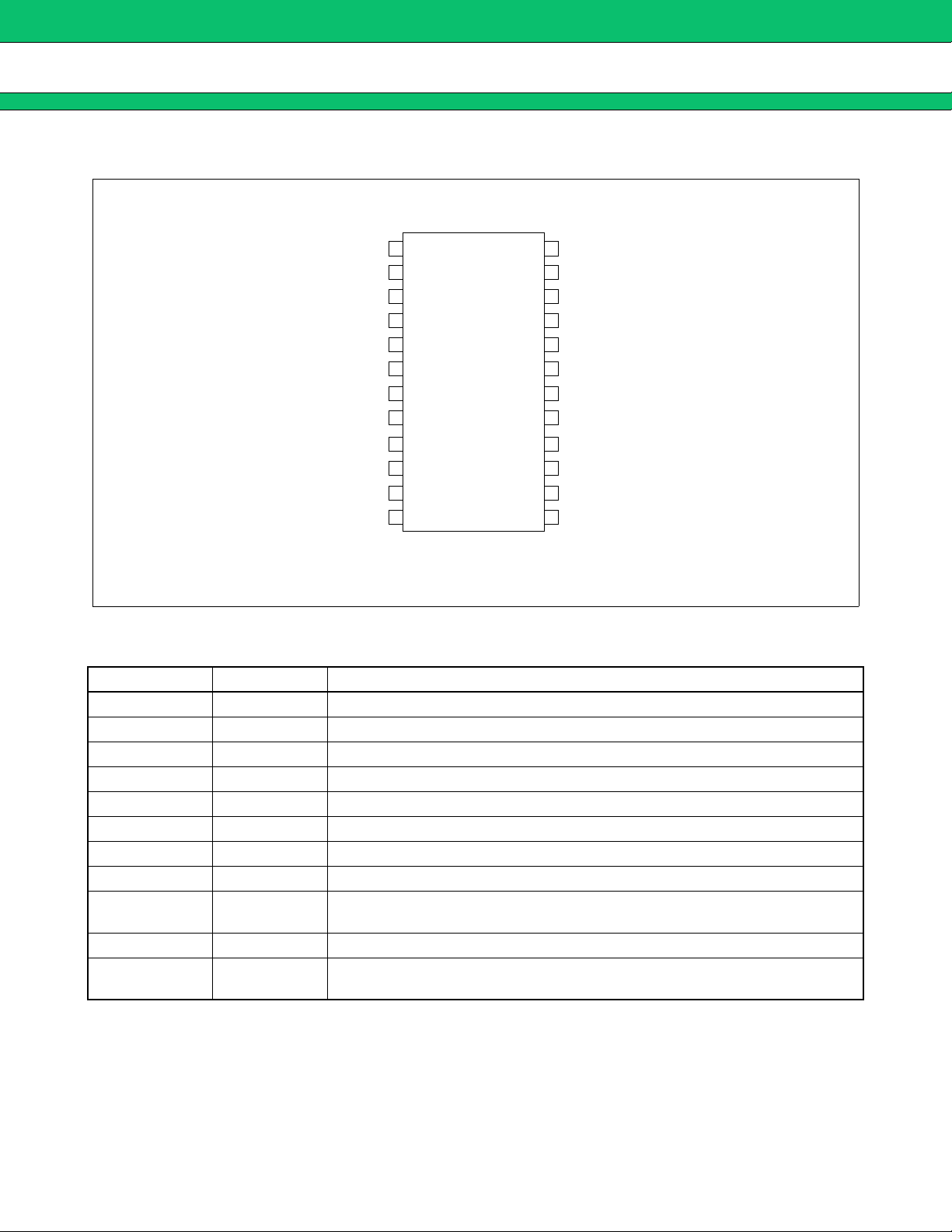
PIN ASSIGNMENT
■
(TOP VIEW)
AVDD
DVDD
AVSS
(LSB) D8
D7
D6
D5
D4
D3
D2
(MSB) D1
DVSS
1
2
3
4
5
6
7
8
9
10
11
12
24
23
22
21
20
19
18
17
16
15
14
13
(FPT-24P-M01)
(FPT-24P-M03)
PIN DESCRIPTION
■
Pin No. Pin name Functions
1, 18 AV
2, 13, 16 DV
DD Analog power supply pins (+5 V)
DD Digital power supply pins (+3 or +5 V)
3, 15, 17, 24 AVSS Analog power ground pins (0 V)
12 DVSS Digital power ground pin (0 V)
4 to 11 D
1 to D8 Digital output pins. D1: MSB, D8: LSB
14 CLK Clock input pin
21 V
19 V
20 V
INA Analog input pin. Input range: VRB to VRT (2 Vp-p between 0.5 to 4 V)
RT Reference voltage input pin (3 V)
REFT
Reference voltage output pin. When connected to VRT, the pin generates
0.6 × AV
DD (3 V).
23 VRB Reference voltage input pin (1 V)
22 V
REFB
Reference voltage output pin. When connected to VRB, the pin generates
0.2 × AVDD (1 V).
AVSS
VRB
VREFB
VINA
VREFT
VRT
AVDD
AVSS
DVDD
AVSS
CLK
DV
DD
Values within ( ) are typical values.
NOTES ON USE
■
• Be sure to bypass the AVDD, DVDD, VRT and VRB pins to the ground using a high-frequency capacitor.
The high-frequency capacitor should be connected as near the pin as possible.
• Provide four clocks or more immediately after the power up to prevent current dissipation due to the
indeterminate internal logic.
2
Page 3
ABSOLUTE MAXIMUM RATINGS (See WARNING)
■
MB40C568
Parameter Symbol
Rating
Min. Max.
Power supply voltage AV
Input voltage
Output voltage D
DD, DVDD –0.3 7.0 V
CLK, V
INA
VRT, VRB
1 to D8 –0.3 DVDD+0.3 V
–0.3 AVDD+0.3 V
Storage temperature Tstg –55 +125 °C
WARNING:
Semiconductor devices can be permanently damaged by application of stress (voltage, current,
temperature, etc.) in excess of absolute maximum ratings. Do not exceed these ratings.
RECOMMENDED OPERATING CONDITIONS
■
Value
Parameter Symbol
Min. Typ. Max.
Analog input voltage V
Analog reference voltage: T V
Analog reference voltage: B V
INA VRB –VRT V
RT – – 4.00 V
RB 0.50 – – V
Analog reference voltage range VRT–VRB 1.90 2.00 2.10 V
Digital "H” level input voltage V
IHD 2.4 – – V
Unit
Unit
Digital “L” level input voltage V
Digital input current I
ILD ––0.8V
ID ––5µA
Clock frequency fCLK 0.1 – 20 MHz
Minimum “H” level clock pulse width
Minimum “L” level clock pulse width
tw
tw
+
–
22.5 – – ns
22.5 – – ns
Operating temperature range Ta –20 – 70 °C
WARNING:
Recommended operating conditions are normal operating ranges for the semiconductor device. All
the device’s electrical characteristics are warranted when operated within these ranges.
Always use semiconductor devices within the recommended operating conditions. Operation outside
these ranges may adversely affect reliability and could result in device failure.
No warranty is made with respect to uses, operating conditions, or combinations not represented on
the data sheet. Users considering application outside the listed conditions are advised to contact their
FUJITSU representative beforehand.
(Continued)
3
Page 4
MB40C568
(Continued)
• When using a single power supply
Parameter Symbol
Power supply voltage AV
• When using dual power supplies
Parameter Symbol
Power supply voltage
WARNING:
Recommended operating conditions are normal operating ranges for the semiconductor device. All
the device’s electrical characteristics are warranted when operated within these ranges.
Always use semiconductor devices within the recommended operating conditions. Operation outside
these ranges may adversely affect reliability and could result in device failure.
No warranty is made with respect to uses, operating conditions, or combinations not represented on
the data sheet. Users considering application outside the listed conditions are advised to contact their
FUJITSU representative beforehand.
Value
Min. Typ. Max.
DD, DVDD 4.75 5.00 5.25 V
Value
Min. Typ. Max.
AV
DD 4.75 5.00 5.25 V
DV
DD 2.70 3.00 3.30 V
Unit
Unit
4
Page 5

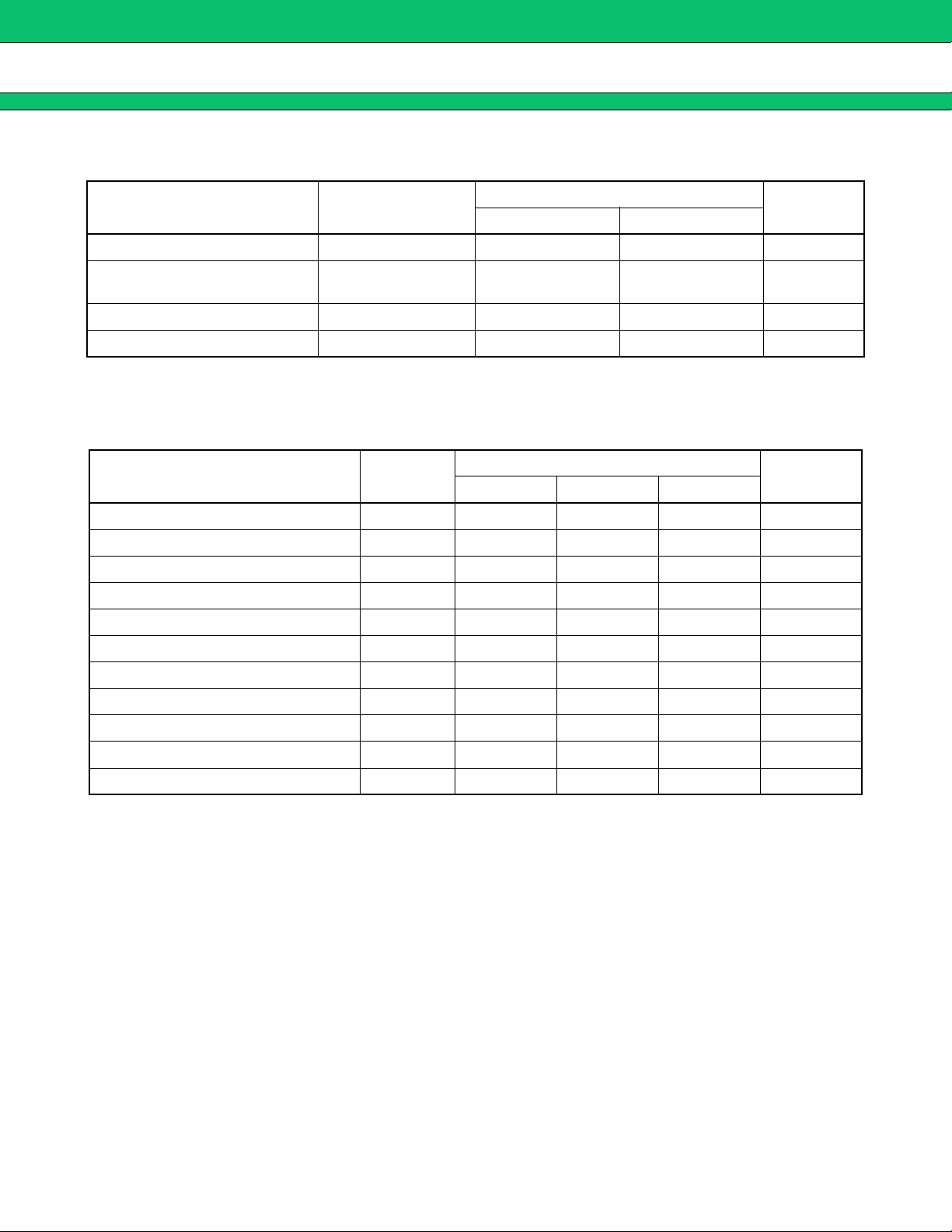
ELECTRICAL CHARACTERISTICS (Using a Single Power Supply)
■
DC Characteristics
(1) Analog section
(AV
DD = DVDD = 4.75 V to +5.25 V, Ta = –20°C to +70°C)
MB40C568
Parameter Symbol
Unit
Min. Typ. Max.
Resolution – – 8 – bit
Value
Linearity error
LE – ±0.20 ±0.30 %
DC precision
Differential linearity error DLE – ±0.12 ±0.20 %
Analog input capacity C
Reference voltage: T V
Reference voltage: B V
INA –15–pF
REFT –0.6 × AVDD –V
REFB –0.2 × AVDD –V
Reference current IRB –16.0 –8.0 –2.0 mA
Analog power supply current AI
Digital power supply current DI
DD – 8.0 14.0 mA
DD –4.07.0mA
(2) Digital section
(AV
DD = DVDD = 4.75 V to +5.25 V, Ta = –20°C to +70°C)
Value
Parameter Symbol
Unit
Min. Typ. Max.
Digital “H” level output voltage V
OHD 4.2 – DVDD V
Digital “L” level output voltage VOLD ––0.4V
Digital “H” level output current I
Digital “L” level output current I
OH –400 – – µA
OL ––1.6mA
(3) Switching section
(AV
DD = DVDD = 4.75 V to +5.25 V, Ta = –20°C to +70°C)
Value
Parameter Symbol
Unit
Min. Typ. Max.
Maximum conversion rate fs 20 – – MSPS
Digital output delay time tpd 0 5 20 ns
5
Page 6

MB40C568
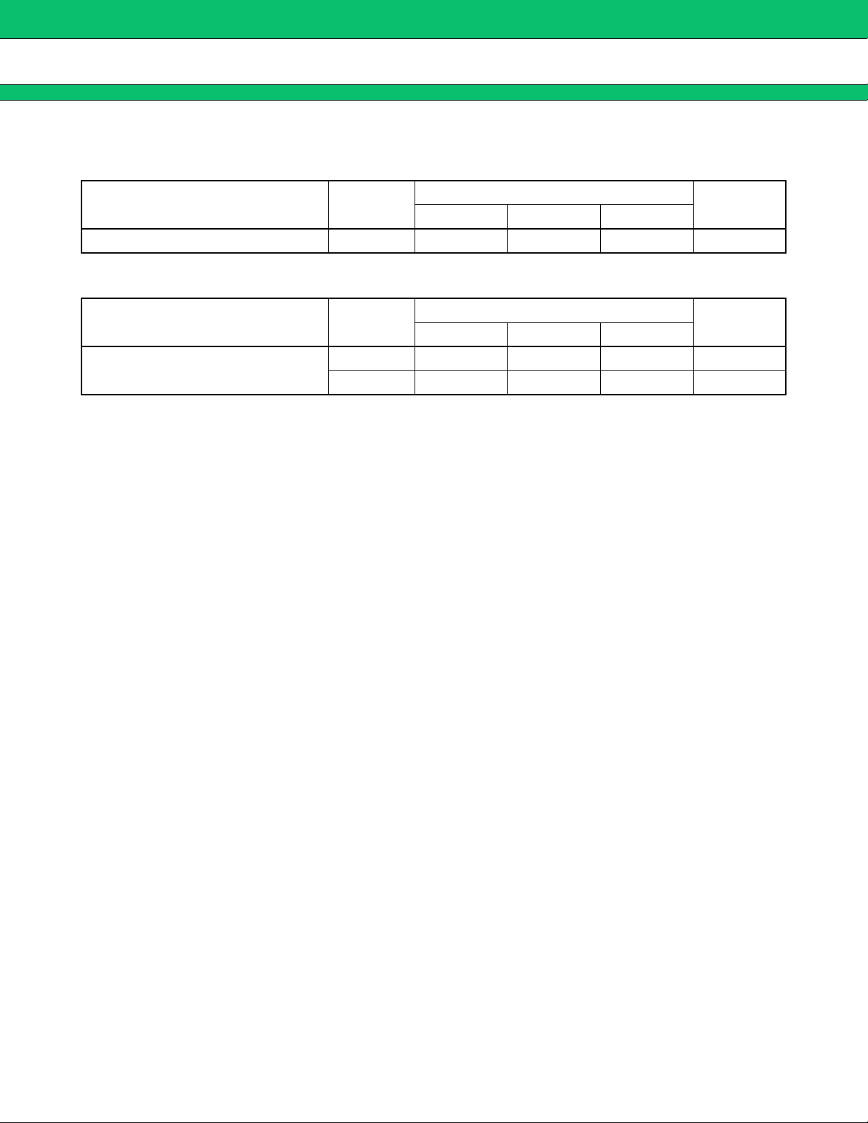
ELECTRICAL CHARACTERISTICS (Using Dual Power Supplies)
■
DC Characteristics
(1) Analog section
(AV
DD = 4.75 V to +5.25 V, DVDD = 2.70 V to +3.30 V Ta = –20°C to +70°C)
Parameter Symbol
Unit
Min. Typ. Max.
Resolution – – 8 – bit
Value
Linearity error
LE – ±0.20 ±0.30 %
DC precision
Differential linearity error DLE – ±0.12 ±0.20 %
Analog input capacity C
Reference voltage: T V
Reference voltage: B V
INA –15–pF
REFT –0.6 × AVDD –V
REFB –0.2 × AVDD –V
Reference current IRB –16.0 –8.0 –2.0 mA
Analog power supply current AI
Digital power supply current DI
DD – 8.0 14.0 mA
DD –3.05.0mA
(2) Digital section
(AV
DD = 4.75 V to +5.25 V, DVDD = 2.70 V to +3.30 V Ta = –20°C to +70°C)
Value
Parameter Symbol
Unit
Min. Typ. Max.
Digital “H” level output voltage V
OHD 2.4 – DVDD V
Digital “L” level output voltage VOLD ––0.4V
Digital “H” level output current I
Digital “L” level output current I
OH –400 – – µA
OL ––1.6mA
(3) Switching section
(AV
DD = 4.75 V to +5.25 V, DVDD = 2.70 V to +3.30 V Ta = –20°C to +70°C)
Value
Parameter Symbol
Min. Typ. Max.
Maximum conversion rate fs 20 – – MSPS
Digital output delay time tpd 0 6 25 ns
6
Unit
Page 7

EQUIVALENT CIRCUIT
■
• Clock input
• Analog input
MB40C568
AVDD
CLK
AVSS
AVDD
VINA
AVSS
• Reference voltage input
VRT
• Reference voltage output
VREFT
• Digital output
DVDD
AVDD
AVSS
AVDD
AVSS
AVDD
VRB
AVSS
AVDD
VREFB
AVSS
DVSS
D1 to D8
7
Page 8

MB40C568
TIMING CHART
■
3 V
CLK
0 V
SAMPLEN SAMPLEN+1
V
INA
VOH
D1 to D8
VOL
DIGITAL OUTPUT BUFFER LOAD CIRCUIT
■
tpd
+
tw
–
tw
1.5 V
0.5 DV
DDDATAN–2 DATAN–1 DATAN
To measurement pin
Measurement point
CL = 15 pF
DV
SS
(Note) CL value includes the floating capacitance of the jig and probe.
8
Page 9

ORDERING INFORMATION
■
Part number Package Remarks
MB40C568
MB40C568PF
MB40C568PFV
24-pin, Plastic SOP
(FPT-24P-M01)
24-pin, Plastic SSOP
(FPT-24P-M03)
9
Page 10

MB40C568
PACKAGE DIMENSIONS
■
24-pin, Plastic SOP
(FPT-24P-M01)
+0.25
+.010
.600
–0.20
15.24
INDEX
1.27(.050)
TYP
"A"
0.10(.004)
13.97(.550)REF
C
1994 FUJITSU LIMITED F24007S-3C-4
–.008
5.30±0.30 7.80±0.40
0.45±0.10
(.018±.004)
(.307±.016)(.209±.012)
Ø0.13(.005)
2.25(.089)MAX
(MOUNTING HEIGHT)
0.05(.002)MIN
(STAND OFF)
+0.40
–0.20
6.80
+.016
–.008
.268
+0.05
–0.02
M
Details of "A" part
0.15
+.002
–.001
.006
0.20(.008)
0.50(.020)
0.18(.007)MAX
0.68(.027)MAX
0.50±0.20
(.020±.008)
Dimensions in mm (inches).
10
(Continued)
Page 11

(Continued)
MB40C568
24-pin, Plastic SSOP
(FPT-24P-M03)
*
7.75±0.10(.305±.004)
INDEX
0.65±0.12(.0256±.0047)
7.15(.281)REF
*
5.60±0.10
+0.10
0.22
–0.05
+.004
.009
–.002
7.60±0.20
(.299±.008)(.220±.004)
*: These dimensions do not include resin protrusion.
+0.20
–0.10
"A"
1.25
.049
0.15
.006
(MOUNTING HEIGHT)
+.008
–.004
0.10(.004)
6.60(.260)
NOM
+0.05
–0.02
+.002
–.001
Details of "A" part
0 to 10°
0 10°
0.10±0.10(.004±.004)
(STAND OFF)
0.50±0.20
(.020±.008)
C
-
-
Dimensions in mm (inches).
11
Page 12

MB40C568
7
FUJITSU LIMITED
For further information please contact:
Japan
FUJITSU LIMITED
Corporate Global Business Support Division
Electronic Devices
KAWASAKI PLANT, 4-1-1, Kamikodanaka
Nakahara-ku, Kawasaki-shi
Kanagawa 211-88, Japan
Tel: (044) 754-3763
Fax: (044) 754-3329
North and South America
FUJITSU MICROELECTRONICS, INC.
Semiconductor Division
3545 North First Street
San Jose, CA 95134-1804, U.S.A.
Tel: (408) 922-9000
Fax: (408) 432-9044/9045
Europe
FUJITSU MIKROELEKTRONIK GmbH
Am Siebenstein 6-10
63303 Dreieich-Buchschlag
Germany
Tel: (06103) 690-0
Fax: (06103) 690-122
Asia Pacific
FUJITSU MICROELECTRONICS ASIA PTE. LIMITED
#05-08, 151 Lorong Chuan
New Tech Park
Singapore 556741
Tel: (65) 281-0770
Fax: (65) 281-0220
All Rights Reserved.
The contents of this document are subject to change without
notice. Customers are advised to consult with FUJITSU sales
representatives before ordering.
The information and circuit diagrams in this document presented
as examples of semiconductor device applications, and are not
intended to be incorporated in devices for actual use. Also,
FUJITSU is unable to assume responsibility for infringement of
any patent rights or other rights of third parties arising from the
use of this information or circuit diagrams.
FUJITSU semiconductor devices are intended for use in
standard applications (computers, office automation and other
office equipment, industrial, communications, and measurement
equipment, personal or household devices, etc.).
CAUTION:
Customers considering the use of our products in special
applications where failure or abnormal operation may directly
affect human lives or cause physical injury or property damage,
or where extremely high levels of reliability are demanded (such
as aerospace systems, atomic energy controls, sea floor
repeaters, vehicle operating controls, medical devices for life
support, etc.) are requested to consult with FUJITSU sales
representatives before such use. The company will not be
responsible for damages arising from such use without prior
approval.
Any semiconductor devices have inherently a certain rate of
failure. You must protect against injury, damage or loss from
such failures by incorporating safety design measures into your
facility and equipment such as redundancy, fire protection, and
prevention of over-current levels and other abnormal operating
conditions.
F9703
FUJITSU LIMITED Printed in Japan
12
If any products described in this document represent goods or
technologies subject to certain restrictions on export under the
Foreign Exchange and Foreign Trade Control Law of Japan, the
prior authorization by Japanese government should be required
for export of those products from Japan.
*DS04-2820
 Loading...