

Page 1

C141-E123-01EN
MAN3184, MAN3367, MAN3735 SERIES
DISK DRIVES
SCSI PHYSICAL INTERFACE SPECIFICATIONS
Page 2

This Product is designed, developed and manufactured as contemplated for general use, including
without limitation, general office use, personal use and household use, but is not designed,
developed and manufactured as contemplated for use accompanying fatal risks or dangers that,
unless extremely high safety is secured, could lead directly to death, personal injury, severe
physical damage or other loss (hereinafter “High Safety Required Use”), including without
limitation, nuclear power core control, airplane control, air traffic control, mass transport operation
control, life support, weapon launching control. You shall not use this Product without securing the
sufficient safety required for the High Safety Required Use. If you wish to use this Product for
High Safety Required Use, please consult with our sale person in charge before such use
The contents of this manual is subject to change without prior notice.
All Rights Reserved. Copyright 2001 FUJITSU LIMITED
Page 3

C141-E123-01EN i
FOR SAFE OPERATION
Handling of This manual
This manual contai ns important i nformation fo r using this p roduct . Rea d thor oughly befor e using
the product. Use this product only after thoroughly reading and understanding especially the
section “Important Alert Items” in this manual. Keep this manual handy, and keep it carefully.
FUJITSU makes every effort to prevent users and bystanders from being injured or from suffering
damage to their property. Use the product according to this manual.
Functional Limitations
There may be certain functional limitations concerning the specifications and functions of the
products co vered by this manual depend ing on the equipment vers ion, especially co ncerning the
following functions.
Versions in which there functions can be used will be communicated through “ENGINEERING
CHANGE REQUEST/NOTICE”, issued by Fujitsu.
Function Equipment Version Which Supports These Functions
Equipment
Version No.
EPROM
Version No.
Standard INQUIRY Data Product
Revision (ASCII)
WRITE RAM Command
These commands cannot be used in the current version.
READ RAM Command
(Proceed to the Copyright Page)
Page 4

C141-E123-01ENii
Related Standards
Specifications and functions of products covered by this manual comply with the following
standards.
Standard (Text) No. Name Enacting Organization
T10/1302D Rev 14
(final)
Working Draft
American National Standard Information
Technology --- SCSI Parallel Interface 3
American National
Standards Institute
(ANSI)
All Rights Reserved, Copyright 2001 Fujitsu Limited
Page 5

C141-E123-01EN iii
REVISION RECORD
Edition Date
published
Revised contents
01 Mar.,2001
Specification No.: C141-E123-**EN
The contents of this manual is subject to
change without prior notice.
All Rights Reserved.
Copyright 2001
FUJITSU LIMITED
Page 6

This page is intentionally left blank.
Page 7

C141-E123-01EN v
PREFACE
This manual explains the MAN3184/MAN3367/MAN3735 series 3-1/2" intelligent disk drives each having
the built-in SCSI controller.
This manual details the specifications and functions of the Small Computer System Interface (SCSI) to
connect the above listed disk drives to the user system. Also, the manual details various SCSI command
specifications and the command processing functions, and provides the information required to creation of
host system software. This manual is int ended to be used b y the users who have the basic knowledge of
computer system operations.
The following lists the manual configuration and the contents of each chapter. The caution labels and
markings are also explained.
Manual Configuratio n and Contents
This manual consists of the following three chapters, and the terminologies and abbreviations sections.
Chapter 1 SCSI Bus
This chapter describes the configuration, physical and electrical requirements, interface protocol, and
other operations of the Small Computer System Interface (SCSI) which connects the
MAN3184/MAN3367/MAN3735 ser i es i nt e lligent disk drives to the user system.
Chapter 2 SCSI Messages
This chapter describes the type and explanation of messages defined for SCSI bus operations.
Chapter 3 ERROR Recovery
This chapter describes error recovery processing executed by the MAN3184/MAN3367/MAN3735 series
intelligent disk drives in response to various errors on the SCSI bus.
Glossary
This section explains the terminologies the reader must understand to read this manual.
Abbreviations
This section lists the abbreviated terms and their full words used in this manual.
Page 8

C141-E123-01ENvi
CONVENTIONS
This manual uses the fo l lowing conventions:
NOTE:
NOTE indicates the information useful for the user to operate the system.
Important information
The important information is provided with the "Important" title. The important information text is
centered so t hat the reader can distinguish it from ot her manual texts. The following gives an example:
IMPORTANT
The IDD operates as a target (TARG) on the SCSI bus. The IDD is
called "TARG" in this chapter except when clear identification is
required.
Notations
A decimal value is indicated as it is in this manual.
A hexadecimal value is indicated in the X'17B9' or 17B9h or 17B9H notation.
A binary value is indicated in the notation similar to "010."
The disk drive model name has a different suffix depending on its SCSI electrical characteristics, capacity,
data format used during shipment and others. The following typical model name is used except when the
model needs to be distinguished. Also, the disk unit may be referred to as the "IDD" or "unit" in this
manual.
Page 9
C141-E123-01EN vii
Note 1:
Model name
M AN 3
184 MC
Interface type MP: Low-Voltage Differential, 16-bit SCSI Ultra-160m,
68-pin connector
MC: Low-Voltage Differential, 16-bit SCSI Ultra-160m,
SCA-2 connector
Formatted capacity (100 MB units)
Disk size
Type AN: 1-inch height (10,025 rpm)
Note 2:
Typical model name
Type model name Model name
MAN3184 MAN3184MP, MAN3184MC
MAN3367 MAN3367MP, MAN3367MC
MAN3735 MAN3735MP, MAN3735MC
Requesting for User's Comments
Please use the User's Comment Form attached to the end of this manual to identify user comments including
error, inaccurate and misleading information of this manual. Contact to your Fujitsu representative for
additional comment forms if required.
Page 10

C141-E123-01ENviii
MANUAL ORGANIZATION
Product/
Maintenance Manual
• General Description
• Specifications
• Data Format
• Installation Requirements
• Installation
• Diagnostics and Maintenance
• Error Analysis
• Principle of Operation
SCSI Physical
Interface
Specifications
• SCSI Bus
• SCSI Message
• Error Recovery
SCSI Logical
Interface
Specifications
• Command Processing
• Data Buffer Management
• Command Specifications
• Parameter Data Formats
• Sense Data and Error Recovery Methods
• Disk Media Management
Page 11

C141-E123-01EN ix
CONTENTS
page
CHAPTER 1 SCSI BUS......................................................................................................................1 - 1
1.1 System Configuration .................................................................................................................. 1 - 1
1.2 Interface Signal Definition...........................................................................................................1 - 3
1.3 Physical Requirements ....................................................................................................... .......... 1 - 7
1.3.1 Interface connector......................................................................................................................1 - 8
1.3.2 Interface cable............................................................................................................................1 - 15
1.4 Electrical Requirements............................................................................................................. 1 - 17
1.4.1 Single-Ended type......................................................................................................................1 - 17
1.4.2 Low-Voltage Differential type................................................................................................... 1 - 20
1.4.3 Internal terminal resistor and power supply for terminating resistor ......................................... 1 - 23
1.4.4 Usage in 8-bit/16-bit transfer mode...........................................................................................1 - 25
1.4.5 Signal driving conditions................................................................................................. .......... 1 - 26
1.5 Timing Rule............................................................................................................................... 1 - 28
1.5.1 Timing value.............................................................................................................................. 1 - 28
1.5.2 Measurement point....................................................................................................................1 - 35
1.6 Bus Phases.................................................................................................................................1 - 39
1.6.1 BUS FREE phase.......................................................................................................................1 - 40
1.6.2 ARBITRATION phase.............................................................................................................. 1 - 41
1.6.3 SELECTION phase ...................................................................................................................1 - 44
1.6.4 RESELECTION phase..............................................................................................................1 - 48
1.6.5 INFORMATION TRANSFER phases.......................................................................................1 - 51
1.6.5.1 Asynchronous transfer mode .....................................................................................................1 - 52
1.6.5.2 Synchronous mode..................................................................................................................... 1 - 55
1.6.5.3 Wide mode transfer (16-bit SCSI) ........................................................................................ ..... 1 - 65
1.6.6 COMMAND phase.................................................................................................................... 1 - 65
1.6.7 DATA phase..............................................................................................................................1 - 65
1.6.8 STATUS phase..........................................................................................................................1 - 68
1.6.9 MESSAGE phase.......................................................................................................................1 - 68
1.6.10 Signal requirements concerning transition between bus phases.................................................1 - 69
1.6.11 Time monitoring feature ............................................................................................................1 - 71
1.7 Bus Conditions ..........................................................................................................................1 - 72
1.7.1 ATTENTION condition ............................................................................................................1 - 72
1.7.2 RESET condition.......................................................................................................................1 - 75
1.8 Bus Phase Sequence ..................................................................................................................1 - 76
Page 12

x C141-E123-01EN
1.9 SCAM........................................................................................................................................ 1 - 84
1.9.1 SCAM operations......................................................................................................................1 - 84
1.10 Ultra SCSI .................................................................................................................................1 - 89
1.10.1 Outline....................................................................................................................................... 1 - 89
1.10.2 Device connection .....................................................................................................................1 - 89
1.10.3 Electrical characteristics of SCSI parallel interface...................................................................1 - 90
1.11 Low-Voltage Differential...........................................................................................................1 - 94
1.11.1 Ultra2-SCSI............................................................................................................................... 1 - 94
1.11.2 Ultra-160M................................................................................................................................1 - 94
1.11.3 LVD driver characteristics.........................................................................................................1 - 94
1.11.4 LVD receiver characteristics .....................................................................................................1 - 95
1.11.5 LVD capacitive loads ................................................................................................................ 1 - 96
1.11.6 System level requirements for LVD SCSI drivers and receivers...............................................1 - 97
1.12 SCSI bus fairness.......................................................................................................................1 - 98
CHAPTER 2 SCSI MESSAGE ..........................................................................................................2 - 1
2.1 Message System...........................................................................................................................2 - 1
2.1.1 Message format............................................................................................................................2 - 1
2.1.2 Message type...............................................................................................................................2 - 2
2.1.3 Message protocol......................................................................................................................... 2 - 4
2.2 SCSI Pointer................................................................................................................ ................ 2 - 5
2.3 Message Explanation...................................................................................................................2 - 8
2.3.1 TASK COMPLETE message: X'00'(T→I).................................................................................2 - 8
2.3.2 SAVE DATA POINTER message: X'02'(T→I).........................................................................2 - 8
2.3.3 RESTORE POINTERS message: X'03' (T→1)..........................................................................2 - 8
2.3.4 DISCONNECT message: X'04' (T→I)........................................................................................2 - 8
2.3.5 INITIATOR DETECTED ERROR message: X'05'(I→T).........................................................2 - 9
2.3.6 ABORT TASK SET message: X'06' (I→T)............................................................................... 2 - 9
2.3.7 MESSAGE REJECT message: X'07'(I↔T)............................................................................. 2 - 10
2.3.8 NO OPERATION message: X'08' (I→T).................................................................................2 - 10
2.3.9 MESSAGE PARITY ERROR message: X'09' (I→T)..............................................................2 - 10
2.3.10 LINKED TASK COMPLETE message: X'0A'(T→I) ..............................................................2 - 11
2.3.11 TARGET RESET message: X'0C' (I→T).................................................................................2 - 11
2.3.12 ABORT TASK message: X'0D' (I→T) ....................................................................................2 - 11
2.3.13 CLEAR TASK SET message: X'0E'(I→T)..............................................................................2 - 11
2.3.14 CONTINUE TASK message: X'12' (I→T) ..............................................................................2 - 12
Page 13

C141-E123-01EN xi
2.3.15 TARGET TRANSFER DISABLE message : X'13' (I→T) .......................................................2 - 12
2.3.16 Task attribute messages.............................................................................................................2 - 13
2.3.17 IGNORE WIDE RESIDUE message: X'23' (T→I)..................................................................2 - 14
2.3.18 IDENTIFY message: X'80' to X'FF' (I↔T)..............................................................................2 - 15
2.3.19 SYNCHRONOUS DATA TRANSFER REQUEST message (I↔T) .......................................2 - 16
2.3.20 WIDE DATA TRANSFER REQUEST message (I↔T)........................................................... 2 - 24
2.3.21 PARALLEL PROTOCOL REQUEST message (I↔T) ............................................................2 - 28
CHAPTER 3 ERROR RECOVERY..................................................................................................3 - 1
3.1 Error Conditions and Retry Procedure.........................................................................................3 - 1
3.2 Recovery Control.........................................................................................................................3 - 6
GLOSSARY
....................................................................................................................................GL
-
1
ABBREVIATION
.................................................................................................................................AB
-
1
Page 14

xii C141-E123-01EN
FIGURES
page
1.1 Example of SCSI configuration...................................................................................................1 - 2
1.2 Interface signals...........................................................................................................................1 - 3
1.3 DATA BUS and SCSI ID ............................................................................................................1 - 4
1.4 SCSI interface connector (IDD side) (16-bit SCSI).....................................................................1 - 8
1.5 SCSI interface connector (cable side) (16-bit SCSI)....................................................................1 - 9
1.6 Single-ended connector pin assignment (16-bit SCSI)...............................................................1 - 10
1.7 Low-Voltage-Differential connector pin assignment (16-bit SCSI)...........................................1 - 11
1.8 SCA-2 type, 16-bit SCSI interface connector (IDD side) ..........................................................1 - 12
1.9 SCA-2 Type, single-ended 16-bit SCSI connector signal assignment........................................1 - 13
1.10 SCA Type, Low-Voltage-Differential connector signal assignment..........................................1 - 14
1.11 Connection of interface cable..................................................................................................... 1 - 16
1.12 Single-Ended SCSI termination circuit-1...................................................................................1 - 17
1.13 Single-Ended SCSI termination circuit-2...................................................................................1 - 18
1.14 LVD SCSI termination circuit....................................................................................................1 - 20
1.15 Circuit for mated indications......................................................................................................1 - 23
1.16 16-bit SCSI (not SCA2) terminating resistor circuit..................................................................1 - 24
1.17 Fast-5/10 Measurement Point ....................................................................................................1 - 35
1.18 Fast-20 Measurement Point........................................................................................................ 1 - 36
1.19 LVD ST Data Transfer measurement point ...............................................................................1 - 37
1.20 LVD DT Data Transfer measurement point...............................................................................1 - 38
1.21 BUS FREE phase.......................................................................................................................1 - 40
1.22 ARBITRATION phase ..............................................................................................................1 - 43
1.23 SELECTION phase....................................................................................................................1 - 47
1.24 RESELECTION phase...............................................................................................................1 - 50
1.25 INFORMATION TRANSFER phase (phase control) ...............................................................1 - 51
1.26 Transfer in asynchronous mode .................................................................................................1 - 54
1.27 ST transfer in synchronous mode...............................................................................................1 - 58
1.28 Data Group Pad field and pCRC field transfer ..........................................................................1 - 64
1.29 Data sequence at data transfer....................................................................................................1 - 65
1.30 Data transfer rate in synchronous mode.....................................................................................1 - 68
1.31 Switching direction of transfer over data bus.............................................................................1 - 70
1.32 ATTENTION condition.............................................................................................................1 - 74
1.33 RESET condition.......................................................................................................................1 - 76
Page 15

C141-E123-01EN xiii
1.34 Bus phase sequence....................................................................................................................1 - 77
1.35 Example of bus phase transition at execution of a single command ..........................................1 - 79
1.36 State of level-1 SCAM target.....................................................................................................1 - 86
1.37 State of level-2 SCAM target............................................................................................... ......1 - 87
1.38 Comparison of active negate current and voltage ......................................................................1 - 92
1.39 Single-ended test circuit.............................................................................................................1 - 93
1.40 LVD transceiver architecture.....................................................................................................1 - 95
1.41 Connection to the LVD receivers...............................................................................................1 - 95
1.42 Differential SCSI bus capacitive loading...................................................................................1 - 96
2.1 Message format............................................................................................................................2 - 2
2.2 SCSI pointer configuration..........................................................................................................2 - 7
Page 16

xiv C141-E123-01EN
TABLES
page
1.1 INFORMATION TRANSFER phase identification....................................................................1 - 6
1.2 Single-Ended maximum distance between terminators................................................................1 - 7
1.3 LVD maximum distance between terminators.............................................................................1 - 8
1.4 SE and LVD Transmission line impedance of cable at maximum indicated
data transfer rate.........................................................................................................................1 - 15
1.5 Attenuation Requiaments for SCSI cable media........................................................................1 - 15
1.6 Output characteristic..................................................................................................................1 - 19
1.7 Input characteristic.....................................................................................................................1 - 19
1.8 LVD DIFFSENS driver specifications.......................................................................................1 - 21
1.9 DIFFSENS receiver operating requirements..............................................................................1 - 21
1.10 Requirements for terminating resistor power supply..................................................................1 - 23
1.11 Setting set up pin, 16-bit (wide)/8-bit (narrow) mode................................................................1 - 25
1.12 Signal status at receiving end.....................................................................................................1 - 26
1.13 Signal driving method ................................................................................................................1 - 26
1.14 Bus phases and signal sources....................................................................................................1 - 27
1.15 SCSI bus control timing values..................................................................................................1 - 28
1.16 SCSI bus data & information phase ST timing values...............................................................1 - 28
1.17 SCSI bus data & information phase DT timing values...............................................................1 - 29
1.18 Parameters used for fast synchronous data transfer mode..........................................................1 - 67
1.19 Retry count setting for RESELECTION phase..........................................................................1 - 71
1.20 Maximum capacitance ...............................................................................................................1 - 97
1.21 System level requirements.........................................................................................................1 - 98
2.1 SCSI message...............................................................................................................................2 - 3
2.2 Extended message........................................................................................................................2 - 4
2.3 Definition of data transfer mode by message exchange.............................................................2 - 17
2.4 Synchronous mode data transfer request setting ........................................................................2 - 19
2.5 Transfer mode setup request from INIT to IDD ........................................................................2 - 21
2.6 Transfer mode setup request from IDD to INIT ........................................................................2 - 23
2.7 Data bus width defined by message exchange...........................................................................2 - 25
2.8 Wide mode setting request from the INIT to the IDD................................................................2 - 27
2.9 Wide mode setting request from the IDD to the INIT................................................................2 - 28
2.10 TRANSFER PERIOD FACTOR field.......................................................................................2 - 29
2.11 Valid protocol options bit combinations....................................................................................2 - 30
Page 17

C141-E123-01EN xv
2.12 PARALLEL PROTOCOL REQUEST message implied agreement..........................................2 - 32
3.1 Retry procedure for SCSI error ....................................................................................................3 - 7
Page 18

This page is intentionally left blank.
Page 19

C141-E123-01EN 1 - 1
CHAPTER 1 SCSI BUS
1.1 System Configuration
1.2 Interface Signal Definition
1.3 Physical Requirements
1.4 Electrical Requirements
1.5 Timing Rule
1.6 Bus Phases
1.7 Bus Conditions
1.8 Bus Phase Sequence
1.9 SCAM
1.10 Ultra SCSI
1.11 Low-Voltage Differential
1.12 SCSI Bus Fairness
This chapter describes the configuration, physical and electrical characteristics, interface protocol, and
operations of SCSI buses.
Note:
The IDD operates as a target (TARG) on the SCSI bus. The IDD is called "TARG" in this
chapter except when clear identification is required.
1.1 System Configuration
Up to 16-bit SCSI series models can be connected to the system via the SCSI bus. Figure 1.1 gives
an example of multi-host system configuration.
Each SCSI device operates as an initiator (INIT) or a target (TARG). Only a single INIT and a
single TARG selected by this INIT can operate simultaneously on the SCSI bus.
The system configuration allows any combination of a SCSI device to operate as the INIT and a
SCSI device to o pe ra te as t he T ARG. Also , a ny devic e ha ving b ot h the I NI T a nd TARG functions
can be used on the SCSI bus.
Each SCSI device is assigned a unique address (or SCSI ID). The SCSI ID corresponds to a bit
number of the SCSI data bus. While the INIT uses a logical unit number (LUN) to select an I/O
unit to be connected under TARG control.
Page 20
C141-E123-01EN1-2
Any SCSI ID of the IDD can be selected using the setup pins. However, the LUN is fixed to zero
(0). The SCSI ID can be 0 to 15.
Note:
The maximum number of SCSI devices and the maximum cable length are limited depending
on the selected SCSI data transfer mode and the SCSI transceiver type. Appropriate SCSI
devices and cable length must be determined for each system.
Figure 1.1 Example of SCSI configuration
Page 21
C141-E123-01EN 1 - 3
1.2 Interface Signal Definition
Figure 1.2 shows interface signal types. The SCSI bus consists of 27 signal lines. The 27 signal
lines consist of data buses (2 bytes plus two odd parity bits) and 9 control signal lines.
The SCSI bus can be a single-ended or low voltage differential(LVD) interface depending on the
model used. Their physical and electrical characteristics are detailed in Sections 1.3 and 1.4.
P_CRCA (18)
Figure 1.2 Interface signals
Page 22
C141-E123-01EN1-4
(1) DB15 to DB00, P1, P_CRCA (Data buses)
The 16-bit SCSI system uses a bidirectional data bus consisting of two-byte data and two odd
parity bits.
MSB (2
15
): DB15, LSB (20): DB00
The data bus is used to transfer a command, data, a status, or a message in the INFORMATION
TRANSFER phase. However, DB15 to DB08 and P1 are used for data transfer only. The data is
transferred only after the WIDE DATA TRANSFER REQUEST or PARALLEL PROTOCOL
REQUEST message has been exchanged and the 16-bit data transfer mode has been established
between the INIT and TARG.
In the ARBITRATION phase, the data bus is used to send a SCSI ID to determine the bus
arbitration priority. In the SELECTION or RESELECTION phase, the data bus is used to send a
SCSI ID of the INIT and TARG. Figure 1.3 shows the relationship between the data buses and
SCSI IDs.
DB15 DB14 DB9 DB8 DB7 DB6 DB5 DB4 DB3 DB2 DB1 DB0
SCSI ID #15
SCSI ID #14
SCSI ID #9
SCSI ID #8
SCSI ID #7
SCSI ID #6
SCSI ID #5
SCSI ID #4
SCSI ID #3
SCSI ID #2
SCSI ID #1
SCSI ID #0
Data bus
(16 bit SCSI)
Figure 1.3 DATA BUS and SCSI ID
(a) DB15 to 0
Sixteen data-bit signals that form the 16-bit DATA BUS.
(b) DB7 to 0
Eight data-bit signals that form the 16-bit DATA BUS.
(c) P1 (ST DATA phase)
A signal sourced by the SCSI device driving the data bus during ST DATA phases. This signal is
associated with the DB(15-8) signals and is used to detect the presence of an odd number of bit
errors within the byte. The parity bit is driven such that the number of logical ones in the byte plus
the parity bit is odd.
Page 23

C141-E123-01EN 1 - 5
(d) P1 (data group transfer enabled)
A signal that shall be continuously negated by the SCSI device driving the DB(15-0) signals and
shall be ignored by the SCSI device receiving the DB(15-0) signals during DT DATA phases.
(e) P_CRCA (PARITY/CRC AVAILABLE) (SELECTION p hase, ST DATA phase, COMMAND phase,
MESSAGE phase, or STATUS phase)
A signal sourced by the SCSI device driving the data bus during these phases. This signal is
associated with the DB(7-0) signals and is used to detect the presence of an odd number of bit
errors within the byte. The parity bit is driven such that the number of logical ones in the byte plus
the parity bit is odd.
The parity bits (P1 and P_CRCA) is op tional for the system. The I DD handles the data bus parity
as follows:
• The IDD has the data bus parity check function, and can enable or disable the parity check.
See Section 5.3.2 "SCSI Parity" of the Product Manual for setup details.
• When valid data is sent to the data bus from the IDD, the parity data is always guaranteed
except for the ARBITRATION phase.
(f) P_CRCA (data group transfer enabled)
A signal sourced by a target during DT DATA phases to control whether a data group field is a pad
field, pCRC field, or data field. When asserted the data group field shall b e pad or pCRC fields
that shall not be transferred to the ULP. When negated the data group field shall be a data field that
shall be transferred to the ULP.
Note:
ULP is "Upper Level Protocol".
Page 24

C141-E123-01EN1-6
(2) BSY (BUSY)
The BSY signal indicates that the SCSI bus is in use. In the ARBITRATION phase, this signal is
used to request for the bus usage priority.
(3) SEL (SELECT)
The SEL signal is used by the INIT to select a TARG (in the SELECTION phase) or by the TARG
to reselect an INIT (in the RESELECTION phase).
(4) C/D (CONTROL/DATA)
This is a combination of I/O and MSG signals, and specifies a type of information transferred on
the data bus. The C/D signal is always driven by the TARG (see Table 1.1).
(5) I/O (INPUT/OUTPUT)
The I/O signal specifies the information transmission direction on the data bus. It is also used to
identify the SELECTION phase or RESELECTION phase. This signal is always driven by the
TARG (see Table 1.1).
(6) MSG (MESSAGE)
A signal sourced by a target to indicate the MESSAGE phase or a DT DATA phase depending on
whether C/D is true or false. Asserted indicates MESSAGE or DT DATA (see Table 1.1).
Table 1.1 INFORMATION TRANSFER phase identification
Signal
C/D MSG I/O
Phase Direction Comment
0 0 0 ST DATA OUT INIT -> TARG
0 0 1 ST DATA IN INIT <- TARG
ST Data phase
0 1 0 DT DATA OUT INIT -> TARG
0 1 1 DT DATA IN INIT <- TARG
DT Data phase
Data phase
1 0 0 COMMAND INIT -> TARG
1 0 1 STATUS INIT <- TARG
1 1 0 MESSAGE OUT INIT -> TARG
1 1 1 MESSAGE IN INIT <- TARG
MESSAGE
Page 25

C141-E123-01EN 1 - 7
(7) REQ (REQUEST)
This is a transmission request from the TARG to the INIT in the INFORMATION TRANSFER
phase.
(8) ACK (ACKNOWLEDGE)
The ACK signal is a response to the REQ signal sent from the INIT to TARG in the
INFORMATION TRANSFER phase.
(9) ATN (ATTENTION)
The ATN signal indicates that the INIT has a message to be sent to the TARG. It is used to
generate an ATTENTION condition.
(10) RST (RESET)
The RST signal is a Reset signal to clear all SCSI devices on the bus (to the RESET condition).
1.3 Physical Requirements
All SCSI devices are connected to each other in a daisy chain. Both ends of the interface cable are
terminated with resistor.
Tables 1.2 and 1.3 define the SCSI bus electrical characteristics (for interface signal
driver/receiver).
Table1.2 Single-Ended maximum distance between terminators
Maximum distance between
terminators (meters)
FAST-5 FAST-10 FAST-20
2 to 4 devices 6 3 3
5 to 8 devices 6 3 1.5
9 to 16 devices 6 3 N/A
Number of
attached devices
Page 26
C141-E123-01EN1-8
Table1.3 LVD maximum distance between terminators
Maximum distance between terminators (meters)
Interconnect
Fast-5 Fast-10 Fast-20 Fast-40 Fast-80
Point-to-point 25 25 25 25 25
Multidrop 12 12 12 12 12
1.3.1 Interface connector
(1) Interface connector of the 16-bit SCSI
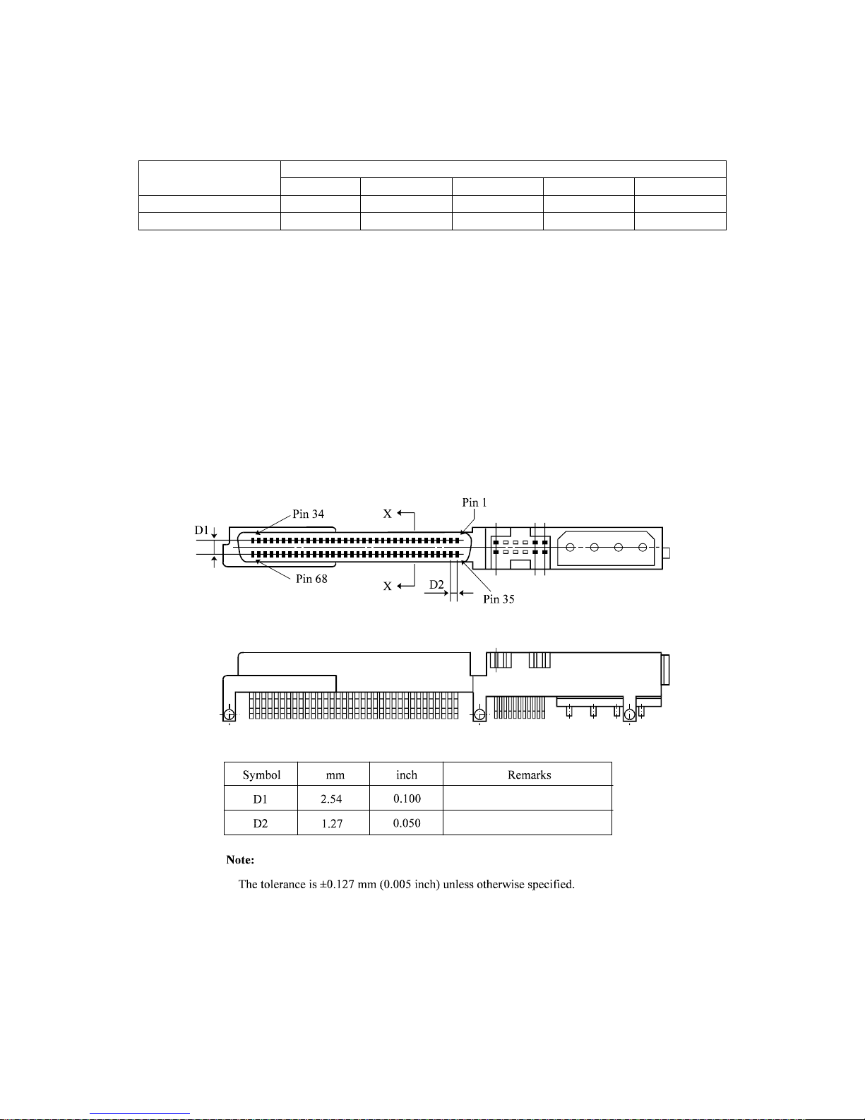
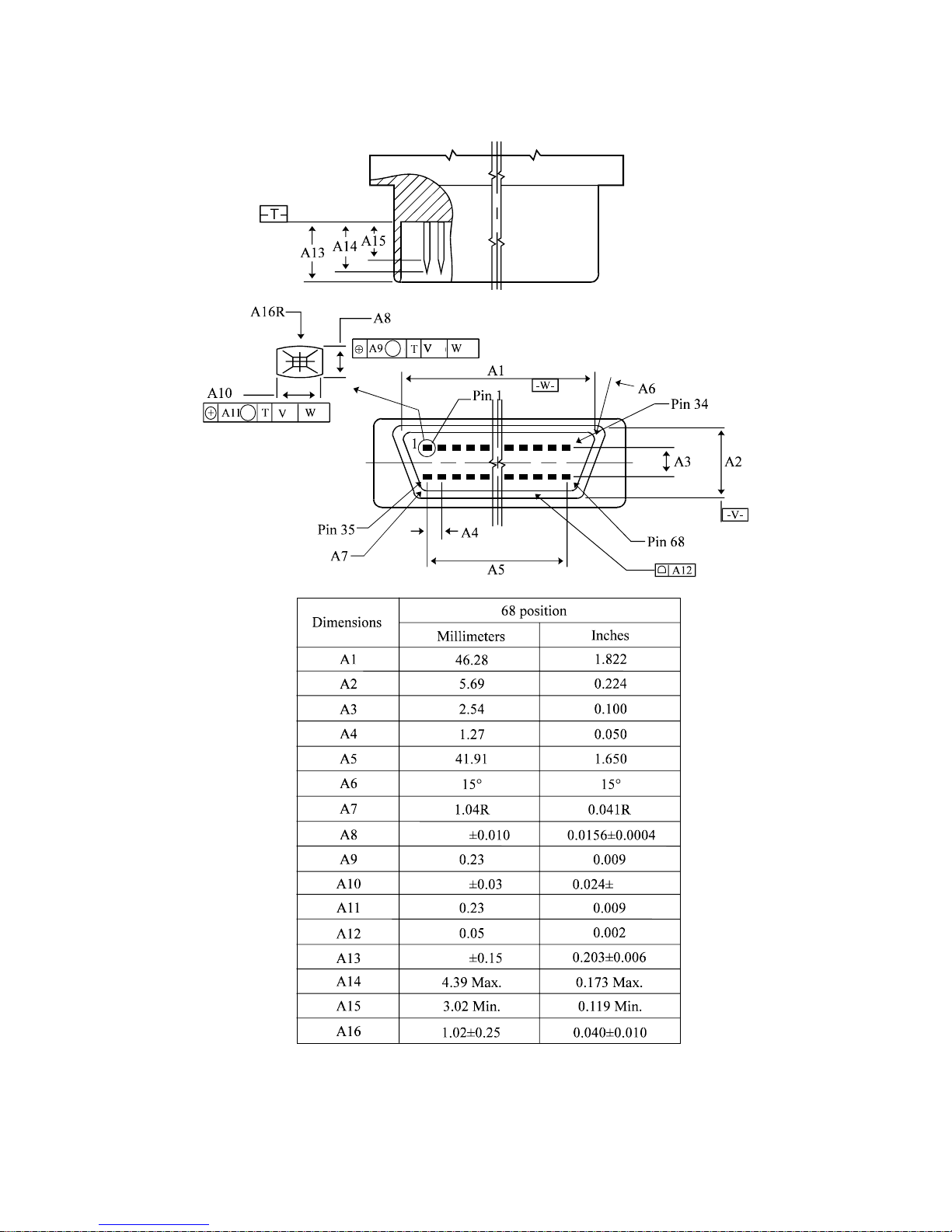
The IDD 16-bit SCSI bus connector is nonshielded 68-pin, consisting of two 34-pin rows with
adjacent pins 1.27 mm (0.05 inch) part (Figure 1.4).
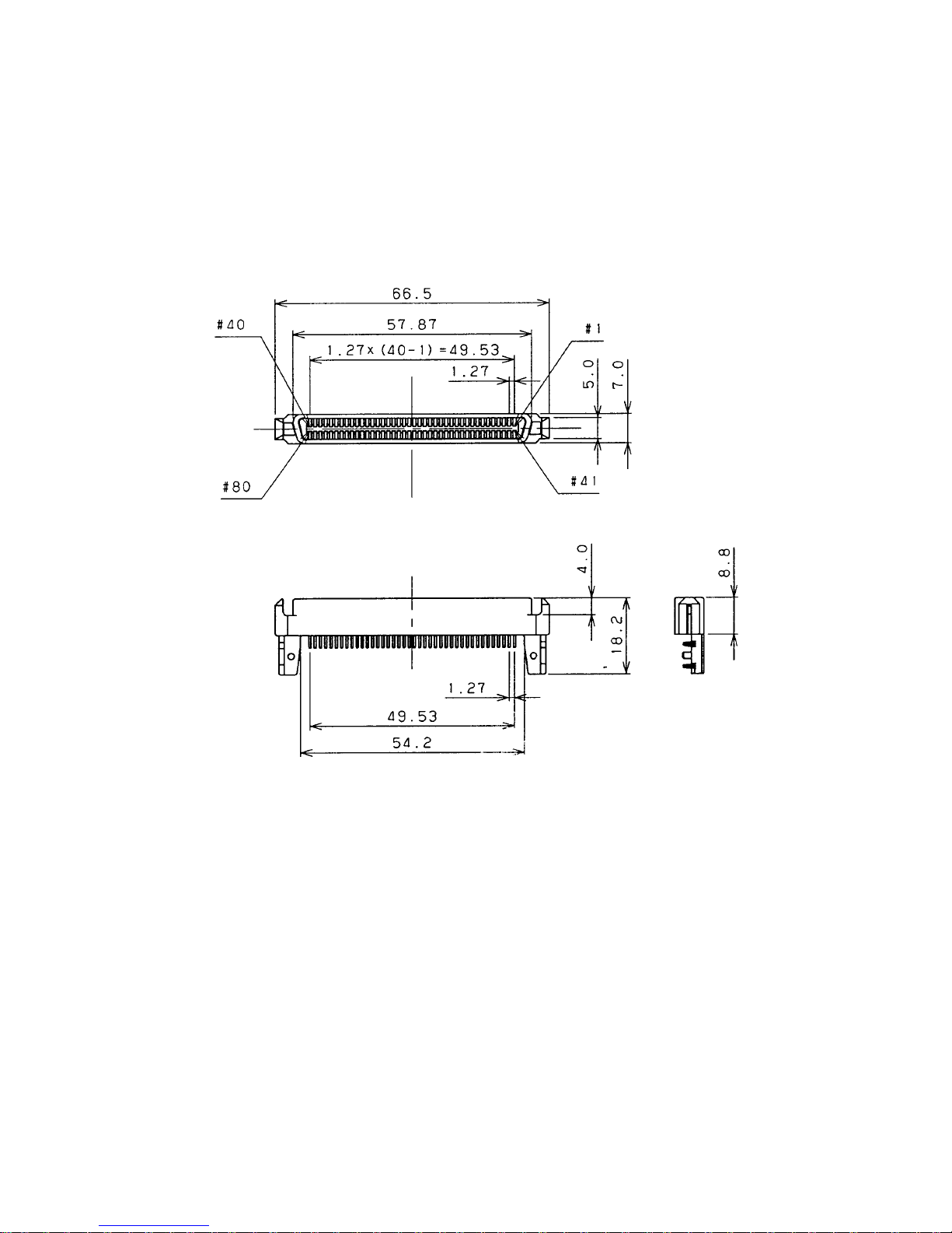
For the interface cable connector, use a nonshielded 68-contact socket consisting of two 34-contact
rows points with adjacent contact points 1.27 mm (0.05 inch) apart (Figure 1.5).
Figure 1.6 shows single-ended interface connector signal assignment.
Figure 1.7 shows low-voltage-differential interface connector signal assignment.
Figure 1.4 SCSI interface connector (IDD side) (16-bit SCSI)
Page 27
C141-E123-01EN 1 - 9
M
M
0.61
5.16
0.001
0.396
Figure 1.5 SCSI interface connector (cable side) (16-bit SCSI)
Page 28

C141-E123-01EN1-10
Pin No. Signal Signal Pin No.
01 GND -DB12 35
02 GND -DB13 36
03 GND -DB14 37
04 GND -DB15 38
05 GND -DBP1 39
06 GND -DB00 40
07 GND -DB01 41
08 GND -DB02 42
09 GND -DB03 43
10 GND -DB04 44
11 GND -DB05 45
12 GND -DB06 46
13 GND -DBP7 47
14 GND -P_CRCA 48
15 GND GND 49
16 GND GND 50
17 TERMPWR * TERMPWR * 51
18 TERMPWR * TERMPWR * 52
19 (reserved) (reserved) 53
20 GND GND 54
21 GND -ATN 55
22 GND GND 56
23 GND -BSY 57
24 GND -ACK 58
25 GND -RST 59
26 GND -MSG 60
27 GND -SEL 61
28 GND -C/D 62
29 GND -REQ 63
30 GND -I/O 64
31 GND -DB08 65
32 GND -DB09 66
33 GND -DB10 67
34 GND -DB11 68
* Terminating resistor power
Figure 1.6 Single-ended connector pin assignment (16-bit SCSI)
Page 29

C141-E123-01EN 1 - 11
Pin No. Signal Signal Pi n No.
01 +DB(12) -DB(12) 35
02 +DB(13) -DB(13) 36
03 +DB(14) -DB(14) 37
04 +DB(15) -DB(15) 38
05 +DB(P1) -DB(P1) 39
06 +DB(0) -DB(0) 40
07 +DB(1) -DB(1) 41
08 +DB(2) -DB(2) 42
09 +DB(3) -DB(3) 43
10 +DB(4) -DB(4) 44
11 +DB(5) -DB(5) 45
12 +DB(6) -DB(6) 46
13 +DB(7) -DB(7) 47
14 +P_CRCA -P_CRCA 48
15 GROUND GROUND 49
16 DIFFSENS GROUND 50
17 TERMPWR * TERMPWR * 51
18 TERMPWR * TERMPWR * 52
19 RESERVED RESERVED 53
20 GROUND GROUND 54
21 +ATN -ATN 55
22 GROUND GROUND 56
23 +BSY -BSY 57
24 +ACK -ACK 58
25 +RST -RST 59
26 +MSG -MSG 60
27 +SEL -SEL 61
28 +C/D -C/D 62
29 +REQ -REQ 63
30 +I/O -I/O 64
31 +DB(8) -DB(8) 65
32 +DB(9) -DB(9) 66
33 +DB(10) -DB(10) 67
34 +DB(11) -DB(11) 68
* Terminating resistor power
Figure 1.7 Low-Voltage-Differential connector pin assignment (16-bit SCSI)
Page 30
C141-E123-01EN1-12
(2) Interface connector of SCA-2 type 16-bit SCSI
The 16-bit, SCA-2 type SCSI bus connectors of the IDD are 80-pin, unshielded connectors, each
having two rows of 40 parallel pins (separated 1.27 mm or 0.05" from each other) (see Figure 1.8).
Figure 1.9 shows the pin assignment of 16-bit, SCA-2 type single-ended SCSI interface connector.
Figure 1.8 SCA-2 type, 16-bit SCSI interface connector (IDD side)
Page 31

C141-E123-01EN 1 - 13
Pin No. S ignal Signal Pin No.
01 +12V (CHARGE) 12V RETURN (GND) 41
02 +12V 12V RETURN (GND) 42
03 +12V 12V RETURN (GND) 43
04 +12V MATED1 44
05 reserved (N.C.) reserved (N.C.) 45
06 reserved (N.C.) GND 46
07 -DB11 GND 47
08 -DB10 GND 48
09 -DB09 GND 49
10 -DB08 GND 50
11 -I/O GND 51
12 -REQ GND 52
13 -C/D GND 53
14 -SEL GND 54
15 -MSG GND 55
16 -RST GND 56
17 -ACK GND 57
18 -BSY GND 58
19 -ATN GND 59
20 -P_CRCA GND 60
21 -DB07 GND 61
22 -DB06 GND 62
23 -DB05 GND 63
24 -DB04 GND 64
25 -DB03 GND 65
26 -DB02 GND 66
27 -DB01 GND 67
28 -DB00 GND 68
29 -DBP1 GND 69
30 -DB15 GND 70
31 -DB14 GND 71
32 -DB13 GND 72
33 -DB12 GND 73
34 5V 5V RETURN (MATED2) 74
35 5V 5V RET URN (GND) 75
36 5V (CHARGE) 5V RETURN (GND) 76
37 Reserved -LED 77
38 RMT_START DLYD_START 78
39 SCSI ID0 SCSI ID1 7 9
40 SCSI ID2 SCSI ID3 8 0
Note:
Signal in parentheses indicates for SCA-2 type.
Figure 1.9 SCA-2 Type, single-ended 16-bit SCSI connecto r signal assignment
Page 32

C141-E123-01EN1-14
Pin No. S ignal Signal Pin No.
01 +12V (CHARGE) 12V RETURN (GND) 41
02 +12V 12V RETURN (GND) 42
03 +12V 12V RETURN (GND) 43
04 +12V MATED1 44
05 reserved(N.C.) reserved(N.C.) 45
06 reserved(N.C.) DIFFSENS 46
07 -DB(11) +DB(11) 47
08 -DB(10) +DB(10) 48
09 -DB(9) +DB(9) 49
10 -DB(8) +DB(8) 50
11 -I/O +I/O 51
12 -REQ +REQ 52
13 -C/D +C/D 53
14 -SEL +SEL 54
15 -MSG +MSG 55
16 -RST +RST 56
17 -ACK +ACK 57
18 -BSY +BSY 58
19 -ATN +ATN 59
20 -P_CRCA +P_CRCA 60
21 -DB(7) +DB(7) 61
22 -DB(6) +DB(6) 62
23 -DB(5) +DB(5) 63
24 -DB(4) +DB(4) 64
25 -DB(3) +DB(3) 65
26 -DB(2) +DB(2) 66
27 -DB(1) +DB(1) 67
28 -DB(0) +DB(0) 68
29 -DB(P1) +DB(P1) 69
30 -DB(15) +DB(15) 70
31 -DB(14) +DB(14) 71
32 -DB(13) +DB(13) 72
33 -DB(12) +DB(12) 73
34 +5V 5V RETURN (MATED2) 74
35 +5V 5V RETURN (GND) 75
36 +5 V (CHARGE) 5V RETURN (GND) 76
37 Reserved -LED 77
38 RMT_START DLYD_START 78
39 SCSI ID0 SCSI ID1 7 9
40 SCSI ID2 SCSI ID3 8 0
Figure 1.10 SCA Type, Low-Voltage-Differential connector signal assignment
Page 33

C141-E123-01EN 1 - 15
1.3.2 Interface cable
Use the twisted-pair interface cables satisfying the requirements of Tables 1.4 ,1.5.
Table 1.4 SE and LVD Transmission line impedance of cable at maximum indicated data transfer
rate
Local SE transmission line
impedance
Local differential
transmission line impedance
Description
Minimum Maximum Minimum Maximum
All
84 Ohms (78
Ohms) (Note)
96 Ohms 110 Ohms 135 Ohms
Note:
If SCSI loads attached to the cable media are separated by more than 1.0 m use the value of 78
Ohms.
Table 1. 5 Attenuation Requiaments for SCSI cable media
Distance between
SCSI bus
terminators (meters)
Distances are consistent with these
minimum size conductors when used
with high quality dielectrics
Notes
0 to 9
0.0324 mm
2
(32 AWG) solid/
0.05092 mm
2
(30 AWG) stranded
multiple loads allowed
0 to 12
0.05092 mm
2
(30 AWG) solid/
0.08042 mm
2
(28 AWG) stranded
multiple loads allowed
>12 to 25
0.05092 mm
2
(30 AWG) solid/
0.08042 mm
2
(28 AWG) stranded
point to point only
A twisted-pair cable must consist of pin n and pin n+1 (where "n" is an odd number) of the
interface connector. Use the SCSI bus cables having the same impedance characteristics to
minimize the signal reflection but keep the highest possible transmission characteristics.
If SCSI devices are connected to the terminals other than the interface cable ends, use the cable
branch at the SCSI connectors. No more SCSI cable can be connected to the last SCSI device
(which is connected to the SCSI bus) except when it is terminated with the terminator (see Figure
1.11).
The interface cable must have the stub length less than 0.1 meter for the single-ended SCSI cable.
Separate the stabs at least 0.3 meter from each other. (Keep the stab at least 30 cm away from a
SCSI device.)
Page 34

C141-E123-01EN1-16
(a) Connection to a middle point of the cable
(b) Connection to the end of the cable.
Figure 1.11 Connection of interface cable
Page 35

C141-E123-01EN 1 - 17
1.4 Electrical Requirements
1.4.1 Single-Ended type
(1) Terminatio n circuit
All signals except for RESERVE, GND, or TERMPWR should be terminated at both ends of the
bus. Each signal should be terminated by one of the following methods. Figures 1.12 and 1.13
show the termination circuit.
a) Each signal must connect to the TE RMPWR signal thro ugh 220 Ω (within ±5%) resistor, and
connect to ground through 330 Ω (within ±5%) resistor.
b) The termination circuit of each signal shall satisfy the following conditions.
1) The terminators should be powered by the TERMPWR line. The circuit may receive
additional power from other sources but not require such additional power for proper
operation;
2) Each terminator should source current to the signal line whenever its terminal voltage is
below 2.5 VDC and this current should not exceed 22.4 mA for any line voltage at or
above 0.5 VDC and 25.4 mA for any line voltage between 0.5 VDC and 0.2 VDC even
when all other signal lines are driven at 4.0 VDC;
3) The voltage on all released signal lines should be at least 2.5 VDC;
4) These conditio ns should be met with any conforming configuration of TARGs and INITs
as long as at least one SCSI device is supplying TERMPWR;
5) The terminator at each end of the SCSI bus should add a maximum of 25 pF capacitance
to each signal;
6) The terminator may not source current to the signal line whenever its terminal voltage is
above 3.24 VDC except terminators may source current when the voltage is above 3.24
VDC in applications where the bus is less than 0.3 m;
Figure 1.12 Single-Ended SCSI termination circuit-1
Page 36

C141-E123-01EN1-18
The IDD uses the terminator circuit satisfying conditions (b) above. The INIT terminator circuit is
also recommended to meet conditions (b) above.
(P_CRCA)
DB
Figure 1.13 Single-Ended SCSI termination circuit-2
Page 37

C141-E123-01EN 1 - 19
(2) Driver and receiver
For the interface signal driver, an open-collector or tri-state buffer that satisfies the following
output characteristics is used. All signals are negative logic (true = "L").
The receiver and non-driver of the SCSI device under the power-on state should satisfy the
following input characteristics on each signal.
Table 1.6 Output characteristic
Driver Type Value Min Max Notes
Passive Negatio n V
OL
0.0 0.5 @IOL=48mA
V
OH
2.5 5.25
Active Negation V
OL
0.0 0.5 @IOL=48mA
V
OH
2.5 3.7
Table 1.7 Input characteristic
Maximum
transfer mode
Min Max Notes
VIL [VDC] - 0.8
VIH [VDC] 2.0 -
Fast-5 IIL [mA] -0.4 0.0 @VI= 0.5VDC
IIH [mA] 0.0 0.1 @VI= 2.7VDC
Minimum input hysteresis [VDC] 0.2 -
VIL [VDC] - 0.8
VIH [VDC] 2.0 - @VI= 0.5VDC
Fast-10
I
IL
[µA]
-20 20 @V
I=
2.7VDC
IIH [µA]
-20 20
Minimum input hysteresis [VDC] 0.3 -
VIL [VDC] - 1.0
VIH [VDC] 1.9 -
Fast-20
I
IL
[µA]
-20 20 @V
I=
0.5VDC
IIH [µA]
-20 20 @V
I=
2.7VDC
Minimum input hysteresis [VDC] 0.3 -
Page 38

C141-E123-01EN1-20
Note:
The SCSI device under the power-off state should satisfy the characteristics of I
IL
and IIH.
[Recommended circuit example]
Driver: MB463 (Fujitsu) or SN7438 (TI) (Open-collector NAND gate)
Receiver: SN74LS240 or SN74LS19 (TI) (Shumitt trigger input inverter)
1.4.2 Low-Voltage Differential type
(1) Terminatio n circuit
All signals except for GROUND and TERMPWR should be terminated at both ends of the bus.
Each signal should be terminated. Figure 1.14 shows the termination circuit.
(P_CRCA)
(P_CRCA)
Figure 1.14 LVD SCSI termination circuit
Page 39

C141-E123-01EN 1 - 21
(2) DIFFSENS
a) DIFFSENS driver
The LVD DFFSENS driver sets a voltage level on the DIFFSENS line that uniquely defines a
LVD transmission mode. LVD terminators and multimode terminators shall provide a LVD
DIFFSENS driver according to the specifications in Table 1.8.
Table 1.8 LVD DIFFSENS driver specifications
Value Max. Nominal Min Notes
VO [V] when IO=0
(shorted to ground) to 5 mA
1.4 1.3 1.2
IOS [mA] 15 5 - With TERMPWR at operational levels
and V
O
=0.
|Input current DC|(µA)
10 - - With terminator disabled.
Input sink current D.C. (µA) at
V
O
=2.75V
200 - 20 Required to prevent the line from
floating and to ensure the HVD
DIFFSENS driver dominate the LVD
b) DIFFSENS receiver
LVD SCSI devices shall incorporate a LVD DIFFSENS receiver that detects the voltage level
on the DIFFSENS line for purposes of informing the device of the transmission mode being
used by the bus. The LVD DIFFSENS receiver shall be capable of detecting SE and LVD
SCSI devices. Table 1.9 define the receiver input levels for each of the two modes.
Table 1.9 DIFFSENS receiver operating requirements
V
IN
range Sensed differential drive type
-0.35 ~ +0.5V SE
+0.7 ~ +1.9V LVD
The input resistance requirement is for purposes of providing gr ound reference if no DIFFSENS
drivers are connected to the bus and to ensure that the DIFFSENS receivers do not load the
DIFFSENS drivers excessively and to ensure that SE mode is detected.
Devices shall not allow the signal drivers to leave the high impedance state during initial power on
until both of the following conditions are satisfied:
Page 40

C141-E123-01EN1-22
a) The device is capable of logical operation for at least 100 ms, and
Notes:
The 100 ms delay allows time for the DIFFSENS pin to connect after the initial power
connection (in the case of insertion of a device into an active system), or allows time for
the power distribution system to settle.
b) The DIFFSENS mode detected has remained stable for an additional 100 ms after a) is
achieved.
A device shall not change its present signal driver or receiver mode based on the DIFFSENS
voltage level unless a new mode is sensed continuously for at least 100 ms.
(3) MATED Signals
If MATED 1 and MATED 2 signals are not mated then one or more short pins are not mated. If
MATED 1 and MATED 2 signals are mated then the mated condition of the short pins is
indeterminate. The MATED 1 and MATED 2 signals may indicate to the SCSI device that the
SCSI device is seated in an SCA-2 connector and it may begin power on processing. The signal
requirements are indicated below, but may be met by the circuit.
a) MATED 2/Drive Side
The signal is attached to signal ground on the SCSI device side.
b) MATED 2/Backplane Side
The signal is attached either directly or through optional logic in such a manner that the
MATED 1 signal is held to a ground level when the MATED 2 connection is completed. The
SCSI device shall sink no more than 100 mA to ground through the MATED 2 pin if opt ional
logic is used.
c) MATED 1/Drive Side
The MATED 1 signal shall be sensed by the SCSI device. When the MATED 1 connection is
determined to be at a ground level, the SCSI device may assume that the SCSI device has been
partially mated. Assuming the mating process continues uninterrupted until competition,
including sensing of the SCSI ID Selection signals and the motor start controls, then normal
power on procedures may begin 250 msec after the MATED 1 signal is observed to transition
to the ground level. When the MATED 1 connection is determined to be at the open level, the
SCSI device is not mated. The MATED 1 signal is tied up to a TTL positive level when the
SCSI device is not installed. If the SCSI device is mated and operating, it may optionally
detect the open level of MATED 1 as an indication that the SCSI device is partially unmated
and may be about to be removed. If the SCSI device supports detection of the open level of
MATED 1 to prepare itself for power removal or for physical removal from the enclosure, the
detection shall occur within 1 second from the time that the Mated 1 open level occurs at the
SCSI device.
Page 41

C141-E123-01EN 1 - 23
(4) MATED 1/Backplane Side
The signal shall be held to a ground level when the MATED 2 connection is completed. The
MATED 1 signal shall be held to the open level when the MATED 2 connection is not completed.
MATED 2
connection
Figure 1.15 Circuit for mated indications
1.4.3 Internal terminal resistor and power supply for terminating resistor
The TERMPWR signal of the interface connector supplies the power to the terminating resistor
circuit connected to both ends of the cable. To attach a terminating resistor to an external SCSI
device or to cut the power of SCSI device having a terminator, the terminator power must be
supplied to the TERMPWR line from any of SCSI devices of the bus. The SCSI device (such as a
host adapter) which always operates as the INIT should supply the power. The terminating resistor
power shall be supplied to the TERMPWR line thr ough a diode to prevent a revers e current.
Table 1.10 lists the requirements for terminating the resistor power supply (Vterm).
Table 1. 10 Requirements for terminating resistor power supply
Terminator Type
SE (P Cable)Terminator Power
Characteristics
0.2V dropout
regulator
LVD
SE and LVD
type
(Multimode)
I
min
(A)@V
min
0.6 0.6 0.5 0.65
V
min
(V)@I
min
2.7 4.0 3.0 3.0
V
max
(V)@ all
conditions
5.25 5.25 5.25 5.25
Page 42

C141-E123-01EN1-24
Figure 1.16 shows the configuration of a SCSI terminating resistor circuit. The circuit shall be set
in either mode (by the CN2 setup pin) depending on the IDD system requirements.
23 24
16-bit SCSI (P-connector) setting terminal
CN2 23-24pin
Supply TERMPWR to SCSI B us Short
Don’t supply TERMPWR to SCSI Bus Open
Figure 1.16 16-bit SCSI (not SCA2) terminating resistor circuit
Notes:
All series have no internal terminator circuit. If the terminator circuit is needed, you
should add the external circuit on your system.
Page 43

C141-E123-01EN 1 - 25
1.4.4 Usage in 8-bit/16-bit transfer mode
When the IDD is used as 8-bit SCSI device, it is connected terminating resistor circuit to upper 8bit and parity (DB08 to DB15 and DBP1) or short set up pin (CN2 13-14). When the IDD is used
as 16-bit SCSI device, leave the set up pin Jumper setting “8/16” open. Table 1.11 shows the
guide. Jumper setting is available only for MP series.
Table 1.11 Setting set up pin, 16-bit (wide)/8-bit (narrow) mode
Transfer mode Jumper setting “8/16” DB08 to DB15 and DBP1
Short Don’t care.
8bit (narrow)
Open
Should be terminated
externally.
16bit (wide) Should be opened Don’t care.
Page 44

C141-E123-01EN1-26
1.4.5 Signal driving conditions
(1) Signal status value
Table 1.12 shows the correspondence between the input interface signal level at the receiving end
and its logic state.
Table 1.12 Signal status at receiving end
Single-ended type signal state
Logic state
Asynchronous, Fast-
5, Fast-10
Fast-20
LVD type signal
state
True, "1", or
asserted
Low (less than 0.8
VDC)
Low (less than 1.0
VDC)
Low (-3.6 to -0.030
VDC)
False, "0", negated
or released
High (more than 2.0
VDC)
High (more than 1.9
VDC)
High (0.030 to 3.6
VDC)
(2) Signal driving method
Two driving methods are available: "OR-tied" type and "non-OR-tied" type as indicated in Table
1.13.
Table 1.13 Signal driving method
Driving method
"OR-tied" type "non-OR-tied" type
Signal status
False (*1) No SCSI device drives a signal.
The signal becomes false when
the terminating resistor circuit
is biased.
A particular SCSI device drives
the signal false. Otherwise, no
SCSI device drives the signal.
True A SCSI de vi ce drives the signal tr ue
*1 In this manual, the signal is said to be false if one of the following conditions is satisfied.
1. The signal is actually driven by a SCSI device to become false (non-OR-tied type).
2. No SCSI device is driving the signal (OR-tied type or non-OR-tied type).
If the BSY, SEL and RST signals may be driven by two or more SCSI devices simultaneously in
the interface operating sequence, they must be driven in the OR-tied method. All signals except
for SEL, BSY, RST and DB(P_CRCA, P1) are not driven by multiple SCSI devices
simultaneously. However, the DBP signals must be driven false in the ARBITRATION phase. All
signals driven in OR-tied and non-OR-tied method can be mixed on the same signal line of SCSI
bus except for BSY, SEL and RST signals.
Page 45

C141-E123-01EN 1 - 27
(3) Signal sources
Table 1.14 lists SCSI device types (or signal sources) which can drive signals in each interface
operating phase.
Table 1.14 Bus phases and signal sources
BSY SEL
I/O,
REQ,
C/D,
MSG
ACK,
ATN
DB7-0
DB15-8,
DBP1
P_CRCA RST
BUS FREE N N N N N N N A
ARBITRATION A W N N ID ID ID A
SELECTION I&T I N I I I I A
RESELECTION I&T T T I T T T A
COMMAND T N T I I N I A
ST DATA IN T N T I T T T A
ST DATA OUT T N T I I I I A
DT DATA IN T N T I T T T A
DT DATA OUT T N T I I I T A
STATUS T N T I T N T A
MESSAGE IN T N T I T N T A
MESSAGE OUT T N T I I N I A
A: Any SCSI device can drive the signal. Also, two or more SCSI devices may drive the
signal simultaneously.
I: Only the INIT SCSI device drives the signal.
I&T: The INIT and TARG SCSI devices drive the signal in the interface operating sequence.
INIT, TARG or both can drive this signal according to the interface sequence.
I or T: The INIT or TARG SCSI device (or both devices) may drive the signal depending on the
I/O signal status and bus width.
ID: Each SCSI device which is actively arbitrating the bus drives a unique data bit
(SCSI ID). The parity bit may be undriven or driven to the true state, but
must never be driven to the false state.
N: Not be driven by any SCSI device.
T: Only the TARG SCSI device drives the signal.
W: Only a single SCSI device selected through arbitra tion drives the signal.
Page 46

C141-E123-01EN1-28
1.5
Timing Rule
1.5.1 Timing value
Table 1.15, 16, 17 give the timing required for operations on the SCSI bus.
Table 1.15 SCSI bus control timing values
Timing description Type Timing values
1 Arbitration Delay min.
2.4µs
2 Bus Clear Delay max. 800 ns
3 Bus Free Delay min. 800 ns
4 Bus Set Delay max.
1.6µs
5 Bus Settle Delay min. 400 ns
6 Cable Skew (1) max. 4 ns
7 Data Release Delay max. 400 ns
8 DIFFSENS voltage filter time min. 100 ms
9 Physical Disconnection Delay min.
200µs
10 Power on to Selection (2) max. 10 s
11 Reset Delay min. 200 ns
12 Reset Hold Time min.
25µs
13 Reset to Selection (2) max. 250 ms
14 Selection Abort Time max.
200µs
15 Selection Time-Out Delay min. 250 ms
16 System Deslew Delay min. 45 ns
Note:
(1) Cable Skew is measured at each device connection with the transmitted skew subtracted from the
received skew. (2) This is a recommended time. It is not mandatory.
Table 1.16 SCSI bus data & information phase ST timing values
Timing values [ns] (5)
Timing descripti on Type
Async Fast-5 Fast-10 Fast-20 Fast-40
1 ATN Transmit Setup Time min. 90 33 33 21.5 19.25
2 ATN Receive Setup Time min. 45 17 17 8.5 6.75
3 Cable Skew (3) max. 4 4 4 3 2.5
4 Receive Assertion Period (4) min. N/A 70 22 11 6.5
5 Receive Hold Time (4) min. N/A 25 25 11.5 4.75
6 Receive Negation Period (4) min. N/A 70 22 11 6.5
7 Receive Setup Time (4) min. N/A 15 15 6.5 4.75
8 Receive REQ (ACK) Period Tolerance min. N/A 1.1 1.1 1.1 1.1
9 Signal Timing Skew max. 8 8 8 5 4.5
10 REQ (ACK) Period min. N/A 200 100 50 25
11 Transmit Assertion Period (4) min. N/A 80 30 15 8
12 Transmit Hold Time (4) min. N/A 53 33 16.5 9.25
13 Transmit Negation Period (4) min. N/A 80 30 15 8
14 Transmit Setup Time (4) min. N/A 23 23 11.5 9.25
15 Transmit REQ (ACK) Period Tolerance max. N/A 1 1 1 1
Note:
(3) Cable Skew is measured at each device connection with the transmitted skew subtracted from the
received skew. (4) See Fig.1-17,18,19 for measurement points for the timing specifications. (5)
SCSI bus timing values specified by the maximum transfer rate for the given range shall apply
even if a slower transfer rate within the given range is negotiated.
Page 47

C141-E123-01EN 1 - 29
Table 1.17 SCSI bus data & information phase DT timing values
Timing values [ns] (8)
Timing descripti on Type
Fast-10 Fast-20 Fast-40 Fast-80
1 ATN Transmit Setup Time min. 48.4 29.2 19.6 14.8
2 ATN Receive Setup Time min. 13.6 7.8 4.9 3.45
3 Cable Skew (6) max. 4 3 2.5 2.5
4 PCRC Receive Hold Time min. 11. 6 5.8 2.9 1.45
5 PCRC Receive Setup Time min. 18.6 12.8 9 .9 8.45
6 PCRC Transmit Hold Time min. 38.4 19.2 9.6 4.8
7 PCRC Transmit Setup Time min. 48.4 29.2 19.6 14. 8
8 Receive Assertion Period (7) min. 80 40 20 8.5
9 Receive Hold Time (7) min. 11.6 5.8 2.9 1.45
10 Receive Negation Period (7) min. 80 40 20 8.5
11 Receive Setup Time (7) min. 11.6 5.8 2.9 1.45
12 Receive REQ (ACK) Period Tolerance max. 0.7 0.7 0.7 0.7
13
Receive REQ Assertion Period with P_CRCA
transitioning
min. 85.5 48 32.5 21
14
Receive REQ Negation Period with P_CRCA
transitioning
min. 85.5 48 32.5 21
15 Signal Timing Skew max. 26.8 13.4 6.7 3.35
16 REQ (ACK) Period min. 200 100 50 25
17 Transmit Assertion Period (7) min. 92 46 23 11.5
18 Transmit Hold Time (7) min. 38.4 19.2 9.6 4.8
19 Transmit Negation Period (7) min. 92 46 23 11.5
20 Transmit Setup Time (7) min. 38.4 19.2 9.6 4.8
21 Transmit REQ (ACK) Period Tolerance max. 0.6 0.6 0.6 0.6
22
Transmit REQ Assertion Period with P_ CRCA
transitioning
min. 97.5 54 35.5 24
23
Transmit REQ Negation Period with P_CRCA
transitioning
min. 97.5 54 35.5 24
Note:
(6) Cable Skew is measured at each device connection with the transmitted skew subtracted from the
received skew. (7) See Fig.1-20 for measurement points for the timing specifications. (8) SCSI bus
timing values specified by the maximum transfer rate for the given range shall apply even if a
slower transfer rate within the given range is negotiated.
(1) ATN transmit setup time
The minimum time provided by the transmitter between the assertion of the ATN signal and the
negation of the ACK signa l .
Specified to provide the increased ATN receive setup time, subject to intersymbol interference,
cable skew, and other distortions.
(2) ATN receive setup time
The minimum time required at the receiver between the assertion of the ATN signal and the
negation of the ACK signal to recognize the assertion of an Attention Condition.
Specified to ease receiver timing requirements.
Page 48

C141-E123-01EN1-30
(3) Arbitration delay
The minimum time a SCSI device shall wait from asserting the BSY signal for arbitration until the
DATA BUS is examined to see if arbitration has been won. There is no maximum time.
(4) Bus clear delay
The maximum time that for a SCSI device to release all SCSI signals after:
a) T he BUS FREE phase is detected (the BSY and SEL signals are both false for a bus settle
delay);
b) The SEL signal is received from another SCSI device during the ARBITRATION phase;
c) The transition of the RST signal to true.
For item a) above, the maximum time for a SCSI device to release all SCSI bus signals is 1200 ns
from the BSY and SEL signals first becoming both false. If a SCSI device requires more than a
bus settle delay to detect BUS FREE phase, it shall release all SCSI bus signals within a bus clear
delay minus the excess time.
(5) Bus free delay
The minimum time that a SCSI device shall wait from its detection of the BUS FREE phase (BSY
and SEL both false for a bus settle delay) until its assertion of the BSY signal in preparation for
entering the ARBITRATION phase.
(6) Bus set delay
The maximum time for a SCSI device to assert the BSY signal and its SCSI ID after it detects a
BUS FREE phase for the purpose of entering the ARBITRATION phase.
(7) Bus settle delay
The minimum time to wait for the bus to settle after changing certain control signals as called out
in the protocol definitions.
Provides time for a signal transition to propagate from the driver to the terminator and back to the
driver.
(8) Cable skew
The maximum difference in propagation time allowed between any two SCSI bus signals measured
between any two SCSI devices excluding any signal distortion skew delays.
(9) Data release delay
The maximum time for an initiator to release the DATA BUS, DB(P_CRCA), DB(P1) signals
following the transition of the I/O signal from false to true.
(10) DIFFSENS voltage filter time
The minimum time DIFFSENS voltage shall be sensed continuously within the voltage range of a
valid SCSI bus mode.
Page 49

C141-E123-01EN 1 - 31
(11) Physical Disconnection delay
The minimum time that a target shall wait after releasing BSY before participating in an
ARBITRATION phase when honoring a DISCONNECT message from the initiator.
(12) Power on to selection
The recommended maximum time from power application until a SCSI target is able to respond
with appropriate status and sense data to the TEST UNIT READY, INQUIRY, and REQUEST
SENSE commands (See SCSI-3 Primary Commands Standard.)
(13) Reset delay
The minimum time that the RST signal shall be continuously true before the SCSI device shall
initiate a reset.
(14) Reset hold time
The minimum time that the RST signal is asserted. There is no maximum time.
(15) Reset to selection
The recommended maximum time from after a reset condition until a SCSI target is able to
respond with appropriate status and sense data to the TEST UNIT READY, INQUIRY, and
REQUEST SENSE commands (See SCSI-3 Primary Commands Standard).
(16) Selection abort time
The maximum time that SCSI device shall take from its most recent detection of being selected or
reselected until asserting the BSY signal in response. This time-out is required to ensure that a
target or initiator does not assert the BSY signal after a SELECTION or RESELECTION phase
has been aborted.
(17) Selection time-out delay
The minimum time that an initiator or target should wait for a assertion of the BSY signal during
the SELECTION or RESELECTION phase before starting the time-out procedure. Note that this
is only a recommended time period.
(18) System deskew delay
The minimum time that a SCSI device should wait after receiving a SCSI signal to ensure that any
signals transmitted at the same time are valid. The system deskew delay shall not be applied to the
synchronous data transfers.
(19) Receive assertion period
The minimum time required at a SCSI device receiving a REQ signal for the signal to be asserted
while using synchronous data transfers provided P_CRCA is not transitioning with pCRC
protection enabled. Also, the minimum time required at a SCSI device receiving an ACK signal
for the signal to be asserted while using synchronous data transfers. For SE fast-5 and fast-10
operation, the time period is measured at the 0.8 V level. For SE fast-20 operation the period is
measured at the 1.0 V level. For LVD see figure 1.19 and 1.20 for signal measurement points.
Page 50

C141-E123-01EN1-32
(20) Receive hold time
For ST data transfers the minimum time required at the receiving SCSI device between the
assertion of the REQ or ACK signal and the changing of the DB(15-0, P_CRCA, and/or P1)
signals while using synchronous data transfers, provided P_CRCA is not transitioning with pCRC
protection enabled.
For DT data transfers the minimum time required at the receiving SCSI device between the
transition (i.e. assertion or negation) of the REQ or ACK signals and the changing of the DB(15-0,
P_CRCA, and/or P1) signals while using synchronous data transfers.
(21) Receive negation period
The minimum time required at a SCSI device receiving a REQ signal for the signal to be negated
while using synchronous data transfers. Also, the minimum time required at a SCSI device
receiving an ACK signal for the signal to be asserted while using synchronous data transfers. For
SE fast-5 and fast-10 operation, the time period is measured at the 2.0 V level. For SE fast-20
operation the period is measured at the 1.9 V level. For LVD see figure 1.19 and figure 1.20 for
signal measurement points.
(22) Receive setup time
For ST data transfers the minimum time required at the receiving SCSI device between the
changing of the DB(15-0, P_CRCA, and/or P1) signals and the assertion of the REQ or ACK
signal while using synchronous data t ransfers.
For DT data transfers the minimum time required at the receiving SCSI device between the
changing of the DB(15-0, P_CRCA, and/or P1) signals and the transition of the REQ or ACK
signals while using synchronous data t ransfers.
(23) Receive REQ(ACK) period tolerance
The minimum tolerance that a SCSI device should allow to be subtracted from the REQ(ACK)
period. The tolerance comprises the Transmit REQ(ACK) tolerance plus a measurement error due
to noise.
(24) Signal timing skew
The maximum signal timing skew occurs when transferring random data and in combination with
interruptions of the REQ or ACK signal transitions (e.g., pauses caused by offsets). The signal
timing skew includes cable skew (measured with 0101...patterns) and signal distortion skew caused
by random data patterns and transmission line reflections. The receiver detection range is the part
of the signal between the “may detect” level and the “shall detect” level on either edge.
(25) REQ (ACK) period
The REQ (ACK) period during synchronous data transfers is measured from an assertion edge of
the REQ (ACK) signal to the next assertion ed ge of the signal. In DT DATA phases the no minal
transfer period for data is half that of the REQ (ACK) period during synchronous data transfers
since data is qualified on both the assertion and negation edges of the REQ (ACK) signal. In ST
DATA phases the nominal transfer period for data is equal to the REQ (ACK) period during
synchronous data transfers since data is only qualified the assertion edge of the REQ (ACK) signal.
Page 51

C141-E123-01EN 1 - 33
(26) Transmit assertion period
The minimum time that a target shall assert the REQ signal while using synchronous data transfers
provided P_CRCA is not transitioning with pCRC pro tection enabled. Also, the minimum time
that an initiator shall assert the ACK signal while using synchronous data transfers.
(27) Transmit hold time
For ST data transfers the minimum time provided by the transmitting SCSI device between the
assertion of the REQ or ACK signal and the changing of the DB(15-0, P_CRCA, and/or P1)
signals while using synchronous data t ransfers.
For DT data transfers the minimum time provided by the transmitting SCSI device between the
transition (i.e. assertion or negation) of the REQ or ACK signals and the changing of the DB(15-0,
P_CRCA, and/or P1) signals while using synchronous data transfers.
(28) Transmit negation period
The minimum time that a target shall negate the REQ signal while using synchronous data transfers
provided P_CRCA is not transitioning with pCRC pro tection enabled. Also, the minimum time
that an initiator shall negate the ACK signal while using synchronous data transfers.
(29) Transmit setup time
For ST data transfers the minimum time provided by the transmitting SCSI device between the
changing of the DB(15-0, P_CRCA, and/or P1) signals and the assertion of the REQ or ACK
signal while using synchronous data t ransfers.
For DT data transfers the minimum time provided by the transmitting SCSI device between the
changing of the DB(15-0, P_CRCA, and/or P1) signals and the transition of the REQ or ACK
signal while using synchronous data t ransfers.
(30) Transmit REQ (ACK) period tolerance
The maximum tolerance that a SCSI device may subtract from the negotiated synchronous period.
The tolerance comprises the transmit REQ (ACK) tolerance plus a measurement error due to noise.
(31) pCRC Receive hold time
The minimum time required at the receiver between the transition of the REQ signal and the
transition of the P_CRCA signal while pCRC protection is enabled.
(32) pCRC Receive setup time
The minimum time required at the receiver between the transition of the P_CRCA signal and the
transition of the REQ signal while pCRC protection is enabled.
Specified to ease receiver timing requirements and ensure that this signal, which is outside CRC
protection, is received correctly.
Page 52

C141-E123-01EN1-34
(33) pCRC Transmit hold time
The minimum time provided by the transmitter between the transition of the REQ signal and the
transition of the P_CRCA signal while pCRC protection is enabled.
(34) pCRC Transmit setup time
The minimum time provided by the transmitter between the transition of the P_CRCA signal and
the transition of the REQ signal while pCRC protection is enabled.
Specified to provide the increased receive setup time, subject to intersymbol interference, cable
skew, and other distortions.
(35) Receive REQ assertion period with P_CRCA transitioning
The minimum time required at a SCSI device receiving a REQ signal for the signal to be asserted
while using synchronous data transfers with P_CRCA transitioning with pCRC protection enabled.
Specified to ensure that the assertion period is longer than the receive hold time plus the receive
setup time.
(36) Receive REQ negation period with P_CRCA transitioning
The minimum time required at a SCSI device receiving an REQ signal for the signal to be negated
while using synchronous data transfers with P_CRCA transitioning with pCRC protection enabled.
Specified to ensure that the negation period is longer than the receive hold time plus the receive
setup time.
(37) Transmit REQ assertion per iod with P_CRCA transitioning
The minimum time that a target shall assert the REQ signal during a DT DATA phase while
transitioning P_CRCA with pCRC protection enabled.
Specified to provide the increased receive REQ assertion period, subject to loss on the
interconnect.
(38) Transmit REQ negation period with P_CRCA transitioning
The minimum time that a target shall negate the REQ signal during a DT DATA phase while
transitioning P_CRCA with pCRC protection enabled.
Specified to provide the increased receive REQ negation period, subject to loss on the
interconnect.
Page 53

C141-E123-01EN 1 - 35
1.5.2 Measurement point
(1) SE Fast-5/10
The measurement point of Fast-5/10 is different from that of Fast-20. The Figure 1.17 is the Fast5/10 measurement point.
Figure 1.17 Fast-5/10 Measurement Point
Page 54

C141-E123-01EN1-36
(2) SE Fast-20
Figure 1.18 is the Fast-20 measurement point.
Figure 1.18 Fast-20 Measurement Point
Page 55

C141-E123-01EN 1 - 37
(3) LVD ST Data Transfer
Figure 1.19 is the LVD ST Data Transfer measurement point.
*
*
**
**
** Use the crossing that yield the shorter Assertion Period
and Negation Period.
Figure 1.19 LVD ST Data Transfer measurement point
Notes:
1. V
N
- negated signal
2. V
A
- asserted signal
3. t
m
= 1,25ns minimum
4. V
A
or VN are required to drive the 100 mV at the leading edge of the transition. Those signals shall be at
least |100 mV| for at least t
m
before and after the transition.
5. Differential voltage signals in all cases.
6. t
af
and tar shall be less than 3 ns.
7. Any signal structure may occur at the receiver while in the t
af
or tar region including sl ope reversal.
Page 56

C141-E123-01EN1-38
(4) LVD DT Data Transfer
Figure 1.20 is the LVD DT Data Transfer measurement point.
*
*
*
*
Figure 1.20 LVD DT Data Transfer measurement point
Notes:
1. V
N
- negated signal
2. V
A
- asserted signal
3. t
m
= 1.25ns minimum
4. V
A
or V
N
are required to drive the 100 mV at the leading edge of the transition. Those signals shall be at
least |100 mV| for at least t
m
before and after the transition.
5. Differential voltage signals in all cases.
6. t
af
and t
ar
shall be less than 3 ns.
7. Any signal structure may occur at the receiver while in the t
af
or t
ar
region including sl ope reversal.
Page 57

C141-E123-01EN 1 - 39
1.6 Bus Phases
The SCSI bus must be in one of the following eight phases:
• BUS FREE phase
• ARBITRATION phase
• SELECTION phase
• RESELECTION phase
• COMMAND phase
• DATA phase
• STATUS phase
• MESSAGE phase
The SCSI bus can never be in more than one phase at any given time.
Note:
In the following bus phase conditions, signals are false unless otherwise defined. Signals on
the timing charts are assumed to be positive logic (or active high).
INFORMATION TRANSFER phase
Page 58

C141-E123-01EN1 - 40
1.6.1 BUS FREE phase
All SCSI devices do not use the bus in the BUS FREE phase. SCSI devices shall detect the BUS
FREE phase after SEL and BSY signals are both false for one Bus Settle Delay.
SCSI devices which have detected the BUS FREE phase shall release all bus signals within one
Bus Clear Delay after BSY and SEL signals become false for Bus Settle Delay. If a SCSI device
requires more than Bus Settle Delay to detect the BUS FREE phase, it shall release all bus signals
within the following period (t):
t = Bus Clear Delay - Period required for BUS FREE phase detection + Bus Settle Delay
The maximum time allowed for releasing the bus after both SEL and BSY becomes false is Bus
Settle Delay + Bus Clear Delay.
Figure 1.21 shows the BUS FREE phase.
Figure 1.21 BUS FREE phase
Page 59

C141-E123-01EN 1 - 41
The SCSI bus enters the BUS FREE phase when the TARG stops the BSY signal in one of the
following events:
• When RESET condition has been detected.
• When TARG has received the following message normally.
ABORT TASK, ABORT TASK SET, CLEAR TASK SET,
LOGICAL UNIT RESET, TARG RESET, CLEAR ACA
• When TARG has transmitted the following message normally.
DISCONNECT, TASK COMPLETE
• When a transceiver mode change.
• When the release of the SEL signal after a SELECTION or RESELECTION phase time-out.
In any case other than above, if the TARG negates the BSY signal to enter a BUS FREE phase, the
TARG informs the INIT that it has detected an ERROR condition of the SCSI bus. The TARG
can enter a BUS FREE phase forcibly regardless of ATN signal status; the INIT must treat that
phase transition as indicating the abnormal end of command. The TARG clears all hold data or
status and terminates the command being executed. It can then create sense data indicating the
detailed error condition. If the INIT detects a BUS FREE phase when it is not expected, it should
issue a REQUEST SENSE command to read the sense data.
1.6.2 ARBITRATION phase
The ARBITRATION phase allows one SCSI device to gain control of the SCSI bus. The SCSI
device that gets control of the SCSI bus can start the operation as INIT or TARG.
This is an optional system bus phase. This phase is required for the system that has two or more
INITs or uses the RESELECTION phase.
Arbitration is mandoratory and requires the detection of a Bus Free phase on the SCSI bus before
starting.
SCSI device with arbitration fairness enabled shall maintain a fairness register which records the
SCSI IDs of devices that need a chance to arbitrate. (see 1.12).
Fairness in arbitration is enabled in targets by the Disconnect-Reconnect mode page.
Figure 1.22 shows the ARBITRATION phase, and the following explains how the SCSI device
gets control of the SCSI bus.
1) The SCSI device shall wait for BUS FREE phase. (see Section 1.6.1).
2) The SCSI device shall wait at least Bus Free Delay after the BUS FREE phase detection before
driving any signal.
3) Then the SCSI device that arbitrates the bus asserts the DATA BUS bit corresponding to its
own SCSI ID and BSY signal (*1) within Bus Set Delay after the last observation of the BUS
FREE phase.
Page 60

C141-E123-01EN1 - 42
4) After waiting at least Arbitration Delay since the SCSI device asserted BSY signal, the SCSI
device shall examine the value on the DATA BUS to determine the priority of the bus
arbitration (*1).
Bus arbitration priority: DB7 (ID#7) > DB6 (ID#6) >... >DB0 (ID#0) >DB15 (ID#15) >DB14
(ID#14) >... >DB8 (ID#8)
• When the SCSI device detects any ID bit which is assigned higher priority than its own
SCSI ID, the SCSI device shall release its signals (BSY and its SCSI ID) then may return
to step (1). (The SCSI device #1 in Figure 1.23 has lost the arbitration.)
• The SCSI device which detects no higher SCSI ID bit on the DATA BUS can obtain the
bus control, then it shall assert SEL signal. (The SCSI device #7 in Figure 1.23 has won
the arbitration.)
• Any other SCSI device that is participating in the ARBITRATION phase shall release its
signals within Bus Clear Delay after SEL signal becomes true, then may return to step (1).
(The SCSI device #3 in Figure 1.21 has lost the arbitration.)
5) The SCSI device which wins arbitration (SCSI device #7 in Figure 1.23) shall wait at least Bus
Clear Delay + Bus Settle Delay after asserting SEL signal before changing any signal state.
*1: When an SCSI device sends its SCSI ID to the DATA BUS, it asserts only the bit at the
position corresponding to its own ID and leaves the other or fifteen bits false. The parity bit
(DBP_CRCA or DBP 1 signal) may be released or asserted, but must not be actively driven
false. The parity bit on the DATA BUS is unpredictable during an ARBITRATION phase.
Page 61

C141-E123-01EN 1 - 43
Figure 1.22 ARBITRATION phase
Page 62

C141-E123-01EN1 - 44
1.6.3 SELECTION phase
An INIT selects a TARG (a single SCSI unit) in the SELECTION phase.
Note:
I/O signal is false during a SELECTION phase. (The I/O signal identifies the phase as
SELECTION or RESELECTION).
(1) Start sequence without ARBITRATION phase
In systems with the ARBITRATION phase not implemented, the INIT starts the SELECTION
phase in the following sequence (see Figure 1.23).
1) The INIT shall wait for at least Bus Clear Delay after BUS FREE phase detection.
2) Then the INIT asserts SCSI IDs of desired TARG and INIT itself on the DATA BUS.
Note:
If single INIT operates without the RESELECTION phase, it is allowed to assert only the
TARG's SCSI ID.
3) After waiting at least Deskew Delay × 2, the INIT a sserts SEL signal and waits the response
(BSY signal) from the TARG.
(2) Start sequence with ARBITRATION phase
In systems with ARBITRATION phase implemented, the INIT starts the SELECTION phase in the
following sequence (see Figure 1.23).
1) The INIT shall wait for at least Bus Clear Delay + Bus Settle Delay after turning SEL signal on
during the ARBITRATION phase.
2) Then the INIT asserts SCSI IDs of the desired TARG and INIT itself on the DATA BUS.
Note:
If single INIT operates without RESELECTION phase, it is allowed to assert only the
TARG's SCSI ID.
3) The INIT releases BSY signal after waiting at least Deskew Delay × 2. The INIT shall then
wait at least Bus Settle Delay before looking for the response (BSY signal) from the TARG.
Page 63

C141-E123-01EN 1 - 45
(3) Selection enabled parity protection and using/without using attention condition
1) The INIT sets the DATA BUS to a value that is the OR of INIT's SCSI ID bit, the TARG's
SCSI ID bit, and the appro priate parity bit(s) (i.e., DB( P_CRCA and/or P1)).
2) In the case of selection using attention condition, the INIT should create an attention condition
(indicating that a MESSAGE OUT phase is to follow the SLECTION phase).
But in the case of selection without using attention condition, the INIT should clear an
attention condition
3) The INIT waits at least two System Deskew Delays and releases the BSY signal.
4) The INT then wait at least one Bus Settle Delay before attempting to detect an assertion of the
BSY signal from the TARG.
(4) Response sequence
When an SCSI device (TARG) detects that the SEL signal and the data bus bit (DBn)
corresponding to the own SCSI ID are true and both BSY and I/O signals are false for at least Bus
Settle Delay, the SCSI device shall recognize that it is selected in the SELECTION phase. At this
time, the selected TARG may sample all bits on the SCSI bus to identify the INIT's SCSI ID.
The TARG must response to the INIT by asserting the BSY signal within Selection Abort Time
since the TARG detects that the TARG is selected. If the SCSI ID with three or more bits is
detected, or if a parity error is detected under the system that the parity bit is enabled, the TARG
shall not respond to the SELECTION phase.
At least Deskew Delay × 2 after the BSY signal (asserted by the TARG) detection, the INIT shall
release SEL signal. The values on the DATA BUS can be changed after this time.
Note:
When Selection without using attention condition, if an INIT detects an unexpected
COMMAND phase, it invalidates all prior negotiations with the selected TARG.
In this case, the INIT should create an attention condition and on the corresponding
MESSAGE OUT phase should issue an ABORT TASK message.
On the next selection of the TARG that received the ABORT TASK message the INIT
should do a selection using the attention condition.
Page 64

C141-E123-01EN1 - 46
(5) Timeout procedure
If the INIT cannot detect the response from TARG when the Selection Timeout Delay or longer
has passed after starting the SELECTION phase, the timeout procedure shall be performed through
one of the following schemes:
a) The case of creating Reset condition
The INIT should assert the RST signal.
b) The case of no response from the selected TARG
1) The INIT should continue asserting the SEL signal.
2) If the INIT creates an attention condition, The INIT should keep ATN signal asserted.
3) The INIT should release DB(15-0,P_CRCA,and/o r P1).
4) If the INIT has not detected the BSY signal to be true after at least one Selection Abort
Time plus two System Deskew Delays, the INIT should release the SEL signal and ATN
signal (if Selection using attention condition) allowing the SCSI bus to go to the BUS
FREE phase.
5) SCSI devices should ensure that when responding to selection was still valid within one
Selection Abort Time of their assertion of the BSY signal.
6) Failure to comply with this requirement could result in an improper selection (two TARG
connected to the same INIT, wrong TARG connected to an INIT, or a TARG connected to
no INIT).
Page 65

C141-E123-01EN 1 - 47
Min. System Deskew Delay × 2 Min. System Deskew Delay × 2
Min. System Deskew Delay × 2
Min. System Deskew Delay × 2
Figure 1.23 SELECTION phase
Page 66

C141-E123-01EN1 - 48
1.6.4 RESELECTION phase
The SCSI device operated as a TARG selects an INIT in the RESELECTION phase. This phase is
an option for the system, and this phase can only be used in systems with the ARBITRATION
phase implemented.
When the TARG re-starts the command processing under the disconnection on the SCSI bus, the
TARG reconnects with the INIT using this phase.
(1) Start sequence
A TARG performs the RESELECTION phase in the following sequence after obtaining control of
the SCSI bus through the ARBITRATION phase (see Figure 1.24).
(a) Parity Protection is disabled
1) TARG waits at least Bus Clear Delay + Bus Settle Delay after asserting the SEL signal in
the ARBITRATION phase.
2) The TARG asserts the I/O signal with sending the SCSI IDs of the TARG itself and INIT
to the SCSI bus (the SCSI device that gets the bus usage right by asserting the I/O signal is
recognized as a TARG).
3) The TARG releases the BSY signal after waiting at least Deskew Delay × 2, and the
TARG shall then wait the response (BSY signal) from the INIT after at least Bus Settle
Delay passed.
(b) Parity Protection Enabled
1) The SCSI device that won arbitration has both the BSY and SEL signals asserted and has
delayed at least one Bus Clear Delay plus one Bus Settle Delay before ending the
ARBITRATION phase.
2) The SCSI device that won arbitration identifies itself as a TARG by asserting the I/O
signal.
3) The TARG also sets the DATA BUS to a value that is the logical OR of TARG's SCSI ID
bit, the INIT's SCSI ID bit and the appropriate parity bit(s).
4) The TARG waits at least two System Deskew Delays and releases the BSY signal.
5) The TARG then waits at least one Bus Settle Delay before attempting to detect an assertion
of the BSY signal by the INIT.
Page 67

C141-E123-01EN 1 - 49
(2) Response sequence
If a SCSI unit (INIT to be selected) detects the SEL and I/O signals and data bus bit (DBn)
corresponding to the own SCSI ID are all true and if it detects the BSY signal which is false for at
least Bus Settle Delay, the SCSI unit shall recognize that it is selected in the RESELECTION
phase. At this time, the selected INIT samples all bits on the data bus to identify the TARG's SCSI
ID.
The INIT shall respond to the TARG by asserting the BSY signal within Selection Abort Time
from the INIT detects that it is selected.
If the SCSI ID in other than two or bits is detected on the data bus or if a parity error is detected on
the system where the parity bit is enabled on the data bus, the INIT shall not respond to the
RESELECTION phase.
When TARG detects the response (BSY signal) from INIT, the TARG asserts BSY signal and
waits at least Deskew Delay × 2, then the TARG releases SEL signal. At this time, the TARG may
change the I/O signal state and value on the SCSI bus.
The INIT shall release the BSY signal after making sure that the SEL signal becomes false.
The TARG should continue asserting the BSY signal until the TARG relinquishes the SCSI bus.
Note:
When the TARG is asserting the BSY signal, a transmission line phenomenon known as a
wired-OR glitch may cause the BSY signal to appear false for up to a round-trip
propagation delay following the release of the BSY signal by the INIT.
This is the reason why the BUS FREE phase is recognized only after both the BSY and
SEL signals are continuously false for a minimum of one Bus Settle Delay.
Page 68

C141-E123-01EN1 - 50
(3) Timeout procedure
If the TARG cannot detect a response (BSY signal) from the INIT when the Selection Timeout
Delay or longer has passed after starting the RESELECTION phase, the timeout procedure shall be
performed though one of the following schemes:
1) The TARG asserts the TRUE signal and generates an RESET condition.
2) The INIT maintains SEL and I/O signals true and stops sending the SCSI ID to the data bus.
Subsequently, the INIT waits for the response from TARG for at least Selection Abort Time +
Deskew Delay × 2. If no response is detected, the INIT releases the SEL and I/O signals
allowing the SCSI bus to go to the BUS FREE phase. If the INIT detects the response from
the TARG during this period, the INIT considers the SELECTION phase to have completed
normally.
The IDD performs process 2) above as RESELECTION phase time-out processing.
Min. System Deskew Delay × 2
+SEL
Figure 1.24 RESELECTION phase
Page 69

C141-E123-01EN 1 - 51
1.6.5 INFORMATION TRANSFER phases
The COMMAND, DATA, STATUS and MESSAGE phases are generally called the
INFORMATION TRANSFER phase. This phase can transfer the control information and data
between the INIT and TARG via the data bus.
The type of INFORMATION TRANSFER phase is determined by the combination of C/D, I/O,
and MSG signals (see Table 1.1). Since these three signals are specified by the TARG, phase
transition is controlled by the SCSI device operating as a TARG. The INIT can request the TARG
to initiate a MESSAGE OUT phase by sending an ATN signal. Besides, the TARG can change the
bus phase to BUS FREE by ceasing the transmission of BSY signal.
During INFORMATION TRANSFER phase, the information transfer is controlled by the REQ
and ACK signals. The TARG sends the REQ signal to request for information transfer, and the
INIT responds to it with the ACK signal. A pair of REQ and ACK signals is used to transfer a
single-byte information on the 8-bit SCSI bus or two-byte information on the 16-bit SCSI bus.
There are two types of information transfer modes: synchronous and asynchronous transfer modes.
They differ from each other by their REQ signal transmission and ACK signal response methods
(called the REQ/ACK handshaking). Also, the 16-bit SCSI bus can transfer 16-bit wide data only
in the DATA phase.
The 16-bit SCSI bus can transfer 16-bit wide data only in the DATA phase except alternate error
detection for the asynchronous information phase (COMMAND, MESSAGE and STATUS). The
detail of these phase is described below section.
The target shall not transition into an information transfer phase unless the REQ/ACK signals are
negated. The target shall not transition from an information transfer phase into another information
transfer phase unless the REQ/ACK signals are negated. During INFORMATION TRANSFER
phase, the TARG shall keep the BSY signal true but keep the SEL signal false. The TARG shall
establish the status of C/D, I/O and MSG signals (which determine the phase type) at least Bus
Settle Delay before the leading edge of REQ signal which requests to transfer the first byte. The
TARG shall keep the status until it detects the trailing edge of the ACK signal which corresponds
to the last byte in that phase (see Figure 1.25).
Figure 1.25 INFORMATION TRANSFER phase (phase control)
Page 70

C141-E123-01EN1 - 52
Notes:
1. After the ACK signal becomes false in the current INFORMATION TRANSFER phase,
the TARG can start preparing a new phase by changing the status of C/D, I/O and MSG
signals. The status of these three signals can change in any order or at once. The status
of one signal may change more than once; however, the TARG should change the status
of each signal only once.
2. A new INFORMATION TRANSFER phase starts when the REQ signal requesting to
transfer the first byte in that phase becomes true. The phase ends when one of C/D, I/O
and MSG signals changes after the ACK signal has changed to false. The period after the
end of phase to the start of next phase (which starts when the REQ signal becomes true) is
not defined.
3. The INIT can predict the next new phase (expected phase) by reading the status change of
C/D, I/O or MSG signal or by reading the type of previously executed phase. However,
the expected phase is made valid only when the REQ signal is changed to true.
1.6.5.1 Asynchronous transfer mode
In asynchronous transfer mode, the INIT and TARG control the information transfer by checking
the status change of REQ and ACK signals (between true and false state) by each other (it is called
the interlock control). The asynchronous transfer can be used in all types of INFORMATION
TRANSFER phase (such as COMMAND, DATA, STATUS and MESSAGE). Figure 1.26 shows
the timing of asynchronous transfer.
If the wide mode data transfer is established between the INIT and TARG, the two-byte data
(DB15 to DB0, DB P 1, DBP _ CRCA) is transfer red on the 1 6-b it SCSI bus. Other wise, single-byte
data (DB7 to DB0, DBP_CRCA) is transferred.
a. Transfer from TARG to INIT
The TARG determines the information transfer direction by the I/O signal. If the I/O signal is
true, the information of the data bus is transferred from the TARG to the INIT . The following
explains the information transfer sequence.
1) The TARG asserts the REQ signal at least one System Deskew Delay + Cable Skew
Delay after sending valid information on the data bus. It must maintain the state of the
data bus until the ACK signal becomes true on the TARG.
2) The INIT fetches the data from the data bus after the REQ signal becomes true. It asserts
the ACK signal to report the completion of reception.
3) After the ACK signal becomes true on the TARG, the TARG negates the REQ signal and
the TARG may change or release the DB(7-0, P_CRCA) or DB(15-0, P_CRCA, P1)
signals.
4) The INIT negates the ACK signal after the REQ signal becomes false.
5) After the ACK signal becomes false, the TARG proceeds to the next byte transfer stage.
Page 71

C141-E123-01EN 1 - 53
b. Transfer from INIT to TARG
When the I/O signal is false, the information of the data bus is transferred from the INIT to the
TARG. The following explains the information transfer sequence.
1) The TARG asserts the REQ signal to request the INIT for information transfer.
2) The INIT asserts the ACK signal at least one System Deskew Delay + Cable Skew Delay
after sending valid information of the requested type on the data bus. The information on
the data bus must be maintained until the REQ signal becomes false on the INIT.
3) The TARG fetches data from the data bus after the ACK signal becomes true, and negates
the REQ signal to report the completion of reception.
4) When the REQ signal becomes false on the INIT, the INIT negates the ACK signal. After
that, the INIT may release o r change the DB(7-0 , P_CRCA) or DB(15-0, P_CRCA, P1)
signals.
5) After the ACK signal becomes false, the TARG proceeds to the next byte transfer stage.
Page 72

C141-E123-01EN1 - 54
Figure 1.26 Transfer in asynchronous mode
Min.
Min.
System Deskew Delay + Cable Skew Delay
System Deskew Delay + Cable Skew Delay
Page 73

C141-E123-01EN 1 - 55
c. Improved Error Detection for the Asynchronous Information Phases (AIP)
The COMMAND, MESSAGE and STATUS asynchronous information transfer phases except
DATA phase only transfer information on the lower eight data bits of a SCSI bus with only
normal parity protection on those transfers. In this improved detection additional check
information can be transferred on the upper eight data bits. This error detection can improve
error detection capabilities. Since the upper eight data bits of the SCSI bus are used for this
scheme, this error detection method is only available on wide SCSI devices that are on wide
SCSI buses.
The additional check information is called "protection code" . This code contains 21-bit code
word and covered signals of the 16-bit SCSI data bus. Protection code checking is enabled or
disabled on an I_T nexus basis. Protection code checking is disabled in the following case:
- After a power cycle
- After a hard reset
- After a TARGET RESET message
- After a change in the transceiver mode (i.e, LVD mode to MSE mode)
A SCSI device enable protection code checking for an I_T nexus when it detects that valid
protection code data is being transmitted on the upper byte of the SCSI bus. The following are
some possible times when a SCSI device could try to enable protection code checking:
- During the first COMMAND, MESSAGE or STATUS phase
- After a UNIT ATTENTION condition
- During the MESSAGE phase of a negotiation
Protection code errors are handled exactly parity errors during COMMAND, MESSAGE or
STATUS phases. But this parity error outputs will be logically OR'd into the existing parity
error logic. There are the some kinds of "parity error" as follows:
- DT mode CRC error
- DBP1, DB15-8 negated
- DBP1, P_CRCA par ity error
- Protection code error
The kind of parity error isn't determined and when the device detected parity error, the device
proceeds to the next procedure without retry. The detail of the procedure is discribed in
CHAPTER 3, ERROR RECOVERY.
1.6.5.2 Synchronous mode
Synchronous data transfer is optional and is only used in DATA phases. It shall be used in a
DATA phase if a synchronous data transfer agreement has been established. The agreement
specifies the REQ/ACK offset and the minimum transfer period.
When synchronous data transfers are being used data may be transferred using ST data transfers or,
optionally, DT data transfers. DT data transfers shall only be used on 16 bit wide buses that
transmit and receive data using LVD transceivers.
The synchronous transfer mode allows information transfer with REQ and ACK signal check by
their pulse count (called the offset interlock). This mode can be used in the DATA phase only.
Page 74

C141-E123-01EN1 - 56
Note:
1. The IDD supports up to 20 MHz (40 MHz on LVD) of synchronous data transfer (see
Table 1.7).
2. The default data transfer mode is asynchronous. When the power is first turned on, the
system is reset, or after the TARGET RE SET message ha s bee n issued , d ata is tr ansfer red
in the asynchronous mode only. It continues until the synchronous transfer mode is
selected by the message exchange explained below.
(1) ST synchronous data transfer
The ST synchronous data transfer is available only when it has been defined between the INIT and
TARG by exchanging the SYNCHRONOUS DATA TRANSFER REQUEST or PARALLEL
PROTOCOL REQUEST message with each other. The following data transfer parameters are
determined and the possible transfer rate between the SCSI units are defined by this message
exchange.
• REQ/ACK Offset: Number of REQ signals that the TARG can send before receiving the ACK
signal.
• Transfer Period: Minimum repetition cycle of REQ and ACK signals.
The TARG can send multiple REQ signal pulses before receiving an ACK signal response if these
pulses do not exceed the limit specified by the REQ/ACK Offset parameter. When the difference
between the REQ and ACK signal pulses has reached this limit at the TARG, the TARG shall not
send a REQ pulse until it receives the leading edge of the next ACK pulse. The data transfer in
DATA phase can complete normally only when the REQ and ACK signal pulses become equal to
each other.
(a) The case of the I/O signal is true (transfer to the INIT)
1) The TARG first drives the DB(7-0,P_CRCA) or DB(15-0,P_CRCA,P1) signals to their
values.
2) The TARG waits at least one Transmit Setup Time.
3) The TARG asserts the REQ signal.
4) T he DB(7-0,P _CRCA) or DB(1 5-0,P_CRCA,P1 ) signals are held valid for a minimum of
one Transmit Hold Time after the assertion of the REQ signal.
5) The TARG asserts the REQ signal for a minimum of one Transmit Assertion Period.
6) T he TARG may then negate the REQ signal and change or release the DB(7-0, P_CRCA)
or DB(15-0,P_CRCA,P1) signals.
7) The INIT reads the value on the DB(7-0,P_CRCA) or DB(15-0,P_CRCA,P1) signals
within one Receive Hold Time of the transition of the REQ signal to true.
8) The INIT then responds with an ACK assertion.
Page 75

C141-E123-01EN 1 - 57
(b) The case of the I/O signal is false (transfer to the TARG)
1) The INIT detects a REQ assertion.
2) The INIT first drives the DB(7-0,P_CRCA) or DB(15-0,P_CRCA,P1) signals to their
values.
3) The INIT delays at least one Transmit Setup Time.
4) The INIT asserts the ACK signal.
5) T he INIT holds the DB (7-0,P_CRCA) or DB(15-0,P_CRCA,P 1) signals valid for at le ast
one Transmit Hold Time after the assertion of the ACK signal.
6) The INIT asserts the ACK signal for a minimum of one Transmit Assertion Period.
7) The INIT may then negate the ACK signal and change or relea se the DB( 7-0, P_CRCA) or
DB(15-0,P_CRCA,P1) signals.
8) The TARG reads the value of the DB(7-0,P_CRCA) or DB(15-0,P_CRCA,P1) signals
within one Receive Hold Time of the transition of the ACK signal to true.
Figures 1.27 shows the timing requirements for ST synchronous mode.
Page 76

C141-E123-01EN1 - 58
[Timing rule for TARG to INIT]
Min. Transmit
Setup Time
Min. Transmit
Hold Time
Min. Transmit
Assertion Period
Min. Received
Hold Time
I/O
REQ
ACK
DB
[Timing rule for INIT to TARG]
Min. Transmit
Setup Time
Min. Transmit
Hold Time
Min. Transmit
Assertion Period
Min. Received
Hold Time
I/O
REQ
ACK
DB
Figure 1.27 ST transfer in synchronous mode
Page 77

C141-E123-01EN 1 - 59
(2) DT synchronous data transfer
When a DT data transfer agreement has been established the target shall only use the DT DATA
IN phase and DT DATA OUT phase for data transfers. The DT synchronous data transfer is
available only when it has been defined between the INIT and TARG by exchanging the
PARALLEL PROTOCOL REQUEST message with each other.
During DT data transfers data shall be clocked on both the assertion and negation of the REQ and
ACK signal lines. References to REQ/ACK transitions in this subclause refer to either an assertion
or a negation of the REQ or ACK signal.
The REQ/ACK offset specifies the maximum number of REQ transitions that shall be sent by the
target in advance of the number of ACK transitions received from the initiator, establishing a
pacing mechanism. If the number of REQ transitions exceeds the number of ACK transitions by
the REQ/ACK offset, the target shall not transition the REQ signal until after the next ACK
transition is received. For successful completion of the DT DATA phase the number of ACK and
REQ transitions shall be equal and both REQ and ACK shall be negated.
Note:
The differences from the ST DATA Synchronous mode are the following: (ST DATA Sync Mode)
1. Only LVD, up to Fast-80 transfer (up to Fast-20, Fast-40 on LVD)
2. 16 bits transfer only (Either 8 bit or 16 bit transfer is available)
3. MSG signal is asserted (MSG signal negat ed)
4. P_CRCA, P1 signals ar e used as Data Group Transfe r enabled.
5. Both edge of the REQ / ACK is available in the data transmission (Only trailing edge is
available)
Data group contains three fields. They are Data field, Pad field, pCRC field. The following
description is about each field transfer.
(a) Data Group Data field transfer from TARG to INIT
The TARG specifies the data transfer direction using the I/O signal. When the I/O signal is true,
data is transferred from the TARG to the INIT. And MSG signal determines the kind of DATA
phase. When the MSG signal is true, the DATA phase is DT DATA phase. The following explains
the transmission sequence. The target shall not transition the REQ signal when the P _CRCA signal
is asserted for the current data group until the initiator has responded with all ACK transitions for
the previous data groups.
1) TARG drives the DB(15 -0) signals to their desired va lues and shall negate the P_CRCA
signal.
2) TARG waits at least the longer of a pCRC transmit setup time from the negation of
P_CRCA or a transmit setup time from DB(15-0 ) signals being driven with valid data.
3) TARG transits the REQ signal and holds the DB(15-0) signals valid for a minimum of a
transmit hold time and the P_CRCA signal for a minimum of a pCRC transmit hold time.
4) TARG holds the REQ signal for at least a transmit assrttion period if asserted or a transmit
negation peri od if negated.
Page 78

C141-E123-01EN1 - 60
5) INIT fetches the values from DB(15-0) signals within a receive hold time of the transition
of the REQ signal and it also fetches the value from the P_CRCA signal within a pCRC
receive hold time of the transition of the REQ signal. Then INIT responds with an ACK
transition.
(b) Data Group Data field transfer from INIT to TARG
When the I/O signal is false, data is transferred from the INIT to the TARG. Other condition is the
same in the section (a).
1) INIT drives the DB(15-0) signals to their desired values after detecting a REQ transition
with P_CRCA signal negated.
2) INIT waits at least a transmit setup time and transits ACK signal.
3) INIT holds the DB(15-0) signals valid for at least a transmit hold time and ACK signal for
a minimum of a transmit assertion period if asserted or a transmit negation period if
negated.
4) TARG fetches the value of the DB(15-0) signals within a receive hold time of the
transition of the ACK.
(c) Data Group Pad field and pCRC field transfer from TARG to INIT
The target determines a pad field is required if the I/O signal is true, the target has completed the
data field transfer of the current data group, and REQ signal is asserted. (Pad field required)
1) TARG waits at least one pCRC transmit hold time since the last REQ assertion to assert
P_CRCA.
2) TARG waits at least one transmit hold time since the last REQ assertion to assert the
DB(15-0) signals to their desired pad values.
3) TARG waits at least the longer of a pCRC transmit setup time from the assertion of
P_CRCA or a transmit setup time from DB(15-0) being driven with valid pad data.
4) TARG waits until the initiator has responded with all ACK transitions for the previous
data group.
5) TARG waits at least one transmit REQ assertion period with P_CRCA transitioning since
the last REQ assertion.
6) TARG negates the REQ signal hold the DB(15-0) signals valid for a minimum of one
transmit hold time and holds the REQ signal negated for a minimum of a transmit negation
period.
7) TARG drives the DB(1 5-0) signals to their desired pCRC values and waits at least one
transmit setup time.
8) TARG asserts the REQ signal and holds the DB(15-0) signals for a minimum of one
transmit hold time and the REQ signal asserted for a minimum of a transmit assertion
period.
Page 79

C141-E123-01EN 1 - 61
9) TARG drives the DB(1 5-0) signals to their desired pCRC values and waits at least one
transmit setup time.
10) TARG negates the REQ signal and holds the DB(15-0) signals for a minimum of one
transmit hold time and the P_CRCA signal asserted for at least a pCRC transmit hold time.
11) TARG holds the REQ signal negated for at least one transmit REQ negation period with
P_CRCA transitioning since the last REQ negation.
If the target determines no pad field is required, the the transmission sequence is the following
way.
1) TARG waits at least one pCRC transmit hold time since the last REQ negation to assert
P_CRCA.
2) TARG waits at least one transmit hold time since the last REQ negation to assert the
DB(15-0) signals to their desired pCRC values.
3) TARG waits at least the longer of a pCRC transmit setup time from the assertion of
P_CRCA or a transmit setup time from DB(15-0) being driven with valid pCRC data.
4) TARG waits until the INIT has responded with all ACK transitions for the previous data
group.
5) TARG waits at least one transmit REQ negation period with P_CRCA transitioning since
the last REQ negation.
6) TARG asserts the REQ signal and holds the DB(15-0) signals valid for a minimum of one
transmit hold time and the REQ signal asserted for a minimum of a transmit assertion
period.
7) TARG drives the DB(1 5-0) signals to their desired pCRC values and waits at least one
transmit setup time.
8) TARG negates the REQ signal and holds the DB(15-0) signals for a minimum of one
transmit hold time and the P_CRCA signal asserted fo r a minimum of one pCRC tra nsmit
hold time.
9) TARG holds the REQ signal negated for at least one transmit REQ negation period with
P_CRCA transitioning since the last REQ negation.
After either of the above sequence is complete the TARG has ended a data Group.
INIT fetches the values from the DB(15-0) signals within one receive hold time of the
REQ signal. And then responds with an ACK transition.
The INIT continues to use the pad bytes, if any, for checking against the computed pCRC
for the current data group. Upon receipt of the last byte of the pCRC field, the received
pCRC and computed pCRC shall be compared. I f they do match (i.e. , no pCRC error).
then the INIT negates the ACK signal.
Page 80

C141-E123-01EN1 - 62
If received pCRC and computed pCRC do not match (i.e., a pCRC er ror is de tected), or if
an improperly formatted data group is transferred, then the INIT creates an attention
condition or before the last transfer of the pCRC field. When the TARG switches to a
MESSAGE OUT phase the INIT sends an INITIATOR DETECTED ERROR message to
the TARG. This message notifies the TARG that data contained within the data group was
invalid.
If the TARG does not retry transferring the information transfer or it exhausts its retry
limit the TARG goes into a STATUS phase and send a CHECK CONDITI ON status with
a sense key set to ABORTED COMMAND and an additional sense code set to
INITIATOR DETE CTED ERROR MESSAGE RECEIVED for the task associated with
the received INITIATOR DETECTED ERROR message.
(d) Data Group Pad field and pCRC field transfer from INIT to TARG
If the I/O signal is false (transfer to the target), the INIT determines the data field transfer is
complete by detecting an assertion of the P_CRCA signal. If the REQ signal is asserted ( i.e., pad
field required) the INIT shall first transfer the two pad bytes, then the four pCRC b ytes. If the RE Q
signal is negated (i.e., no pad field required) the INIT shall tr ansfer the four pCRC bytes.
Pad field data and pCRC field data are transferred using the same negotiated values as the data
field data.
The TARG may continue to send REQs, up to the negotiated offset, for the ne xt data group . The
TARG shall not transition REQ with P_CRCA asserted until the initiator has responded with all
ACK transitions for the previous data group.
When the INIT detects a n asser tion o f the P _CRCA signal a nd the RE Q signal is asse rte d ( i.e ., pa d
field required), the transmission sequence is the following way.
1) Transfer data bytes for all outstanding REQs received prior to the REQ that had the
P_CRCA signal asserted. IN IT drives the DB(1 5-0) signals to their desire d pad values.
2) INIT delays at least one transmit setup time, negates the ACK signal and holds the DB(15-
0) signals valid for a minimum of one transmit hold time and the ACK signal negated for a
minimum of a transmit assertion period.
3) INIT drives the DB(15-0) signals to their desired pCRC values, delays at least one
transmit setup time, asserts the ACK signal and holds the DB(15-0) signals valid for a
minimum of one transmit hold time and the ACK signal asserted for a minimum of a
transmit assertion period.
4) INIT drives the DB(15-0) signals to their desired pCRC values and delays at least one
transmit setup time.
5) INIT negate s the ACK signal and ho lds the DB( 15-0) si gnals valid fo r a minimum of one
transmit hold time and the ACK signal negated for a minimum of a transmit assertion
period.
Page 81

C141-E123-01EN 1 - 63
When the INIT detects an assertion o f the P_CRCA signal and the REQ signa l is negated (i.e ., no
pad field required),
1) INIT transfers data bytes for all outstanding REQs received prior to the REQ that had the
P_CRCA signal asserted. INIT drives the DB(15-0) signals to their desired pCRC values.
2) INIT delays at least one transmit setup time, asserts the ACK signal and holds the DB(15-
0) signals valid for a minimum of one transmit hold time and the ACK signal asserted for a
minimum of a transmit assertion period.
3) INIT drives the DB (15-0) signals to their desired pCRC values and d elays at least one
transmit setup time.
4) INIT ne gates the ACK signa l and ho lds the DB (15 -0) signals valid fo r a minimum of o ne
transmit hold time and the ACK signal negated for a minimum of a transmit assertion
period.
After either of the above sequence is complete the TARG has ended a data group.
As a result of a data group always being an even number of transfers, the REQ and ACK
signals are negated both before and after the transmission of the data group. The TARG
fetches the value of the DB(15-0) signals within one receive hold time of the transition of
the ACK signal.
The INIT uses the pad bytes, if any, in the generation of the transmitted pCRC. The
TARG then uses those pad bytes, if any, for checking against the co mputed pCRC for the
current data group. Upon receipt o f the last byte of the pCRC field, the received pCRC
and computed pCRC is compare d.
If received pCRC and computed pCRC do not match (i.e., a pCRC er ror is de tected), or if
an improperly formatted data group is transferred, then the associated data group is
considered invalid.
If the TARG does not retry transferring the information transfer or it exhausts its retry
limit the TARG goes into a STATUS phase and send a CHECK CONDITI ON status with
a sense key set to ABORTED COMMAND and an additional sense code set to SCSI
PARITY ERROR for the task associated with the pCRC error.
Page 82

C141-E123-01EN1 - 64
data value pad value pCRC value pCRC value
REQ
DB15-0
P_CRCA
transmit REQ assertion
period with pCRCA
transitioning
transmit negation
period
transmit assertion
period
transmit REQ negation
period with pCRCA
transitioning
transmit hold
pCRC
transmit hold
transmit setup
pCRC
transmit setup
pCRC
transmit hold
pCRC value pCRC valuedata value
+ 100 mV
- 100 mV
0 V
+ 100 mV
- 100 mV
<Pad field required>
<Pad field no required>
P_CRCA
DB15-0
REQ
+ 100 mV
+ 100 mV
+ 100 mV
- 100 mV
- 100 mV
- 100 mV
0 V
0 V
pCRC receive
hold
pCRC receive
setup
receive
setup
receive
hold
ACK
+ 100 mV
- 100 mV
0 V
Figure 1.28 Data Group Pad field and pCRC field transfer
Page 83

C141-E123-01EN 1 - 65
1.6.5.3 Wide mode transfer (16-bit SCSI)
The wide mode transfer enables information transfer using a multiple-byte-wide data bus. It is
used only in DATA phases.
In wide mode transfer, the WIDE DATA TRANSFER REQUEST or PARALLEL PROTOCOL
REQUEST message should first be exchanged by the INIT and the TARG to define the data
transfer mode between SCSI devices. When the WIDE DATA TRANSFER REQUEST or
PARALLEL PROTOCOL REQUEST message is exchanged, a data bus width is determined.
Figure 1.29 shows the data sequence at data transfer. When a wide data transfer agreement is
negotiated in PARALLEL PROTOCOL REQUEST data bus width is determined 16 bit mode
automatically.
Note:
The IDD supports 8-bit and 16-bit transfer modes. The initial value of the data bus width is
"8-bit mode". After power is turned on, a RESET condition occurs, or a TARGET RESET
message is received, data is transferred using 8-bit mode until the mode is switched to "16 -bit
mode" by exchanging the WIDE DATA TRANSFER REQUE ST message.
Number of information
items transferred
P cable
1 Unused A “8-bit mode”
2 Unused B
DB15.................DB8 DB7..................DB0
1 B A “16-bit mode”
Figure 1.29 Data sequence at data transfer
1.6.6 COMMAND pha se
The COMMAND phase is a bus phase in which the TARG requests the INIT to transfer command
information (CDB) to the TARG. The TARG keeps the C/D signal true and the I/O and MSG
signals false during REQ/ACK handshaking in this p hase.
1.6.7 DATA phase
The DATA phase is divided into DATA IN and DATA OUT phases according to the direction of
data transfer. In a DATA phase, synchronous data transfer can be performed.
(1) DT DATA IN phase
The DT DATA IN phase allows the target to request that data be sent to the initiator from the
target using DT data transfers. The target shall assert the I/O and MSG signals and negate the C/D
signal during the REQ/ACK handshake(s) of this phase.
Page 84

C141-E123-01EN1 - 66
(2) DT DATA OUT phase
The DT DATA OUT phase allows the target to request that data be sent from the initiator to the
target using DT data transfers. The target shall assert the MSG signal and negate the C/D and I/O
signals during the REQ/ACK handshake(s) of this p hase.
(3) ST DATA IN phase
The ST DATA IN phase allows the target to request that data be sent to the initiator from the target
using ST data transfers. The target shall assert the I/O signal and negate the C/D and MSG signals
during the REQ/ACK handshake(s) of this phase.
(4) ST DATA OUT phase
The ST DATA OUT phase allows the target to request that data be sent from the initiator to the
target using ST data transfers. The target shall negate the C/D, I/O, and MSG signals during the
REQ/ACK handshake(s) of this phase.
Page 85

C141-E123-01EN 1 - 67
(5) Data transfer rate in synchronous mode
Table 1.18 lists the synchronous transfer mode parameters valid for the IDD. The actual values are
determined by exchange of SYNCHRONOUS DATA TRANSFER REQUEST or PARALLEL
PROTOCOL REQUEST message between the two SCSI devices. If two or more INITs are used,
different parameters may be used by each INIT. The PARALLEL PROTOCOL REQUEST
message are used to negotiate a synchronous data transfer agreement, a wide data transfer
agreement, and set the p rot oco l opt ions b etween two SCSI devic es. Although the d ata tra nsfer r ate
is determined by the Transfer Period parameter, an appropriate REQ/ACK Offset parameter value
must be selected depending on the ACK pulse response of the INIT. The interface cable length
must also be considered.
Table 1.18 Parameters used for fast synchronous data transfer mode
Transfer rate
Parameter type Selectable value
8-bit mode 16-bit mode
X’09’(12.5ns) (4)
Maximum 160.00 MB/s
X'0A' (25 ns) (3) Maximum 80.00 MB/s
X'0B' (37.5 ns) (3) Maximum 53.30 MB/s
X'0C' (50 ns) (2) Maximum 40.00 MB/s
X'11' (75 ns) (2) Maximum 26.66 MB/s
X'19' (100 ns) (1) Maximum 20.00 MB/s
X'1F' (120 ns) (1) Maximum 16.00 MB/s
X'25' (150 ns) (1) Maximum 13.33 MB/s
X'2B' (175 ns) (1) Maximum 11.42 MB/s
X'32' (200 ns) Maximum 10.00 MB/s
X'38' (225 ns) Maximum 8.88 MB/s
X'3E' (250 ns) Maximum 8.00 MB/s
X'44' (275 ns) Maximum 7.27 MB/s
X'4B' (300 ns) Maximum 6.66 MB/s
X'51' (325 ns) Maximum 6.15 MB/s
X'57' (350 ns) Maximum 5.71 MB/s
PPR
Transfer Period
(5)
X'5D' (375 ns)
N/A
Maximum 5.33 MB/s
X'0A' (25 ns) (3) Maximum 40.00 MB/s Maximum 80.00 MB/s
X'0B' (37.5 ns) (3) Maximum 26.60 MB/s Maximum 53.30 MB/s
X'0C' (50 ns) (2) Maximum 20.00 MB/s Maximum 40.00 MB/s
X'11' (75 ns) (2) Maximum 13.33 MB/s Maximum 26.66 MB/s
X'19' (100 ns) (1) Maximum 10.00 MB/s Maximum 20.00 MB/s
X'1F' (120 ns) (1) Maximum 8.00 MB/s Maximum 16.00 MB/s
X'25' (150 ns) (1) Maximum 6.67 MB/s Maximum 13.33 MB/s
X'2B' (175 ns) (1) Maximum 5.71 MB/s Maximum 11.42 MB/s
SDTR
Transfer Period
(6)
X'32' (200 ns) Maximum 5.00 MB/s Maximum 10.00 MB/s
(1) Fast synchronous data transfer mode (Fast SCSI)
(2) Ultra fast synchronous data transfer mode (Fast-20 SCSI)
(3) Ultra-2 fast synchronous data transfer mode only for LVD (Fast-40 SCSI)
(4) Ultra-160M fast synchronous data transfer mode only for LVD (Fast-80 SCSI). This code is
only valid if the PROTOCOL OPTIONS field has a value selected that supports double-
transition data transfers.
(5) PPR : PARALLEL PROTOCOL REQUEST
(6) SDTR : SYNCHRONOUS DATA TRANSFER REQUEST
Page 86

C141-E123-01EN1 - 68
Figure 1.30 Data transfer rate in synchronous mode
1.6.8 STATUS phase
In a STATUS phase, the TARG requests to transfer status information from the TARG to the
INIT. The TARG keeps the C/D and I/O signals true and the MSG signal false during REQ/ACK
handshaking in this phase.
1.6.9 MESSAGE phase
The MESSAGE phase is divided into MESSAGE IN and MESSAGE OUT phases depending on
the direction of message information transfer. In either phase, several messages can be transferred.
The first byte transferred in a MESSAGE phase must be a single-byte message or the first byte of a
multiple-byte message. If the message consists of more than one byte, all bytes must be transferred
in a single MESSAGE phase. For details of message types and their operation, refer to Chapter 2.
(1) MESSAGE IN phase
In a MESSAGE IN phase, the TARG requests to transfer message information from the TARG to
the INIT. T he T ARG ke ep s the C/D, I /O, and MS G signa ls tr ue d uri ng RE Q/ ACK ha nd shaking i n
this phase.
(2) MESSAGE OUT phase
In a MESSAGE OUT phase, the TARG requests to transfer message information from the INIT to
the TARG. The TARG keeps the C/D and MSG signals true and I/O signal false during
REQ/ACK handshaking in this phase.
The TARG executes this phase in response to the ATTENTION condition (described in Section
1.7.1) created by the INIT, and must remain in the MESSAGE OUT phase.
Page 87

C141-E123-01EN 1 - 69
Note:
The TARG can terminate the MESSAGE OUT phase even when the ATN signal is true when
it returns a MESSAGE REJECT message to reject an illegal or invalid message, when it enters
the BUS FREE phase as directed by the received message, or when it returns a message
immediately in response to a received message (such as the SYNCHRONOUS DATA
TRANSFER REQUEST).
The TARG can process a received message immediately if no parity error is detected. If a parity
error is detected, the TARG shall ignore all messages which have been received after the parity
error detected in the MESSAGE OUT phase.
When the TARG receives all message information correctly without detecting a parity error, the
TARG shall enter the INFORMATION TRANSFER phase other than the MESSAGE OUT phase
and execute at least one byte of information transfer in order to request the INIT not to retry
message transfer. During some message transfer, the TARG may report the normal completion of
message reception by switching to the BUS FREE phase (for example, ABORT TASK SET and
TARGET RESET message s).
1.6.10 Signal requirements concerning transition between bus phases
If an SCSI bus is at an intermediate point of two INFORMATION TRANSFER phases (during
transition of bus phase), the interface signals must satisfy the following requirements.
a) The BSY, SEL, and ACK signals must not change.
b) The REQ signal must not change until it is asserted to qualify the start of a new phase.
c) The C/D, I/O, MSG and DB(1 5-0, P_CRCA, P1) signals may change.
d) Switching the DB(15-0, P_ CRCA) signals direction from OUT (INIT driving) to IN (T ARG
driving)
1) The transition of the I/O signal to true.
2) The TARG delays driving the DB(15-0, P _CRCA, and/o r P1 ) by at least one Data Release
Delay plus one Bus Settle Delay after asserting the I/O signal.
3) The IN IT releases the DB(15-0, P_CRCA, and/or P1) within one Data Release De la y
e) Switching the DB(15-0, P_ CRCA and /or P1) directio n from IN (TARG driving) to OUT (INIT
driving)
1) T he TARG negates the I/O signal.
2) The TARG releases the DB(15-0, P_CRCA and/or P1) within one System Deskew Delay.
3) The INIT de tects the negation of the I/O signal.
4) The I N IT asserts the DB(15 -0 , P_CRCA and/or P1) more than o ne System Deskew Delay.
Page 88

C141-E123-01EN1 - 70
f) The P_CRCA signal direction may switch direction while the DATA BUS and/or DB (P 1 ) d oes
not (e.g., changing from COMMAND phase to DT DATA OUT phase).
• When switching the P_CRCA signal direction from out (INIT driving) to in (TARG
driving)
1) The TARG delays driving the P_CRCA by at least one Data Release Delay plus one
Bus Settle Delay after negating the C/D signal
2) The INIT releases the P_CRCA signal within one Data Release Delay after the
transition of the C/D signal to false.
• When switching the P_CRCA signal direction from in (TARG driving) to out (INIT
driving)
1) The TARG releases the P_CRCA signal within one System Deskew Delay after
asserting the C/D signal.
2) The INI T negates the P_CRCA signal more than one System Deskew Delay after the
detection of the assertion of the C/D signal.
g) The ATN and RST signals may change as defined under the descriptions for the attention
condition and hard reset.
Figure 1.31 Switching direction of transfer over data bus
Page 89

C141-E123-01EN 1 - 71
1.6.11 Time monitoring feature
The IDD has a time monitoring feature for the SCSI bus to prevent the hang-up of the SCSI bus in
the case that the IDD cannot receive a response from the INIT in the RESELECTION phase.
The IDD monitors the response from the INIT (BSY signal) in the RESELECTION phase. When
the IDD cannot receive the response within a specified period (250 ms), the IDD executes the
timeout process (see Section 1.6.4) and releases the SCSI bus once. After that the IDD executes
the retry process of the RESELECTION phase (see Section 3.1).
The user can select the number of retries of the RESELECTION phase by the CHANGE
DEFINITION command.
Table 1.19 Retry count setting for RESELECTION phase
RSRTY bit
Retry count for
RESELECTION phase
"0" 10 times
"1" (Se t ting at shipping)
∞ (Unlimited)
For details on setting, refer to Subsection 3.1.4, in the SCSI Logical Interface Specifications.
Page 90

C141-E123-01EN1 - 72
1.7 Bus Conditions
Two types of asynchronous control, the ATTENTION condition and RESET condition, shall be
defined to control or modify the bus phase transition sequence (bus conditions).
1.7.1 ATTENTION conditi on
The ATTENTION condition allows the INIT to report that the INIT has a message to be sent to
the TARG. The TARG receives the message from the INIT by starting the MESSAGE OUT
phase. Figure 1.32 shows the ATTENTION condition.
(1) Generation and release of ATTENTION condition (INIT)
The INIT can generate the ATTENTION condition by asserting the ATN signal except for the
ARBITRATION or BUS FREE phase.
When generating of an attention condition on the SELECTION phase following arbitration, the
INIT must set the ATN signal true at least System Deskew Delay × 2 before releasing the BSY
signal.
When generating of a new ATTENTION condition in the INFORMATION TRANSFER phase, to
inform the TARG of the ATTENTION condition before the transition to the next new bus phase,
the INIT must set the ATN signal true before ATN transmit setup time or more from the timing of
setting false the ACK signal for the last byte being transferred in the current bus phase. If the ATN
sending timing is delayed, the TARG may not be informed of the ATTENTION condition until the
next bus phase. The INIT may not operate as it should.
When transferring message information in several bytes in the MESSAGE OUT phase, the INIT
must keep the ATN signal true. The INIT can make the ATN signal false any time except while
the ACK signal is true in the MESSAGE OUT phase. When transferring the last byte in the
MESSAGE OUT phase, the INIT generally makes the ATN signal false during the period between
the time the REQ signal becomes true and the time it replies the ACK signal. In this case, the INIT
must set the ATN signal false before Deskew Delay × 2 or more form the timing of setting true the
ACK signal.
The INIT must make the ATN signal false before making the ACK signal true to transfer the last
message byte if so specified for the particular type of m essage to the TARG. (See Su bsection 2.1.2.)
(2) Response against ATTENTION condition (TARG)
The TARG shall start the MESSAGE OUT phase and respond to the ATTE NTION condition in
the following conditions. Also, the TARG shall enter the MESSAGE OUT phase when the ATN
signal is true after the TARG returns the MESSAGE REJECT or other message with halting the
MESSAGE OUT phase.
• When the ATN signal becomes true in the COMMAND phase, the TARG shall start the
MESSAGE OUT phase immediately after a part or all bytes of command (CDB) has been
transferred.
Page 91

C141-E123-01EN 1 - 73
• When the ATN signal becomes true in the DATA phase, the TARG shall start the MESSAGE
OUT phase immediately after the DATA phase. However, the TARG can enter the
MESSAGE OUT phase any time when necessary. (Data transfer is not interrupted on a
boundary of logical data blocks.) The INIT shall continue the REQ/ACK handshaking (in
DATA phase) until the bus phase is changed.
• When the ATN signal becomes true in the STATUS phase, the TARG shall start the
MESSAGE OUT phase after the end of status byte transfer.
• When the ATN signal becomes true in the MESSAGE IN phase, the TARG shall start the
MESSAGE OUT phase immediately after the end of current message transfer.
• When the ATN signal becomes true in the SELECTION phase, the selected TARG shall start
the MESSAGE OUT phase immediately after the SELECTION phase.
• When the ATN signal becomes true in the RESELECTION phase, the TARG shall start the
MESSAGE OUT phase after the end of IDENTIFY message transfer.
During a RESELECTION phase the INIT should only create an attention condition to transmit an
ABORT TASK SET, ABORT TASK, T ARGET RESET, CLEAR TASK SET, DISCONNECT,
LOGICAL UNIT RESET, or NO OPERATION message. Other uses may result in ambiguities
concerning the nexus.
In the case of more than one byte message transferred, the INIT should keep the ATN signal
asserted througho ut the MESSAGE OUT phase.
Unless otherwise specified, the INIT may negate the ATN signal at any time, that does not violate
the specified setup and hold times, except it must not negate the ATN signal while the ACK signal
is asserted during a MESSAGE OUT phase.
Normally, the INIT negates the ATN signal while the REQ signal is true and the ACK signal is
false during the last REQ/ACK handshake of the MESSAGE OUT phase.
Page 92

C141-E123-01EN1 - 74
ATN transmit setup time.
Min. System
Deskew
Delay × 2
Figure 1.32 ATTENTION condition
Note:
The ATTENTION condition generated by the INIT determines the message level to be used in
the command execution sequence. (Details are explained in Section 2.1.3.) If the
ATTENTION condition is not generated, the TARG uses a TASK COMPLETE message only.
Page 93

C141-E123-01EN 1 - 75
1.7.2 RESET condition
The RESET condition allows all SCSI devices to release immediately from the bus. RESET has
higher priority than any other phases and bus conditions. Any SCSI device can generate the
RESET condition anytime by keeping the RST signal true for Reset Hold Time or more. The state
of all bus signals except RST signals are undefined during the RESET condition.
All SCSI devices shall stop driving all bus signals (except for the RST signal) and release the bus
within Bus Clear Delay after the RST signal becomes true. After the RESET condition, the SCSI
bus always enters the BUS FREE phase. Figure 1.33 shows the RESET condition.
The following are the IDD operations when the RESET condition is detected.
1) Clears all commands including the currently executing commands and queued commands.
2) Releases the reserved disk state of the disk drive.
3) Initializes the operation mode to its initial status just after power-on if it has been set by the
messa ge or command.
• The current value of the parameter set by the MODE SELECT command is initialized to
the saved value previously established. If the value is not saved, it is initialized to the
default value.
• The synchronous transfer parameters defined between the IDD and other SCSI device are
cleared. Any data transfer mode between all SCSI devices is initialized to the
asynchronous mode.
4) The UNIT ATTENTION conditio n is generated for all SCSI devices.
5) The sense data is no longer retained and is cleared.
6) All data read into the data buffer in advance by the read-ahead cache feature is invalidated.
Notes:
1. The IDD does not generate a RESET condition.
2. The IDD provides only "hard" RESET condition specified by the SCSI standard.
3. Reset Hold Time is specified to guarantee that any SCSI device can recognize the
occurrence the RESET condition. On the IDD, even if the pulse width is less than Reset
Hold Time, the RESET condition is effective.
Page 94

C141-E123-01EN1 - 76
Figure 1.33 RESET condition
1.8 Bus Phase Sequence
The SCSI bus phases are switched in the specific sequence depending on the command execution
by the TARG. When the TARG asserts the BSY signal true in the SELECTION or
RESELECTION phase, the status change of SCSI bus is controlled by the TARG except for the
ATTENTION and RESET conditions.
The RESET condition can stop all bus phases and force the SCSI bus to switch to the BUS FREE
phase. Also, it can switch the bus from any phase to the BUS FREE phase.
Note:
The TARG can enter the BUS FREE phase in order to repo rt an error condition. For d etails,
see Section 1.6.1.
Figure 1.34 shows the allowable bus phase sequence. Figure 1.35 provides an example of bus
phase sequence during single command execution.
Note:
Figure 1.34 shows the bus phase sequence applied to the system which uses the
ARBITRATION phase and the system which does not use the phase. Also, this figure
compares the operations when the MESSAGE OUT phase is used and when it is not used.
The use of MESSAGE OUT phase is determined by the generation of ATTENTION condition
by the INIT. If the ATTENTION condition is not generated, the TARG assumes that the INIT
does not support any message other than the TASK COMPLETE and the TARG uses only the
TASK COMPLETE message in the subsequent command sequence.
Page 95

C141-E123-01EN 1 - 77
Figure 1.34 Bus phase sequence (1 of 2)
Page 96

C141-E123-01EN1 - 78
Figure 1.34 Bus phase sequence (2 of 2)
Page 97

C141-E123-01EN 1 - 79
Figure 1.35 Example of bus phase transition at execution of a single command (1 of 5)
Page 98

C141-E123-01EN1 - 80
Figure 1.35 Example of bus phase transition at execution of a single command (2 of 5)
Page 99

C141-E123-01EN 1 - 81
RESELECTION
Figure 1.35 Example of bus phase transition at execution of a single command (3 of 5)
Page 100

C141-E123-01EN1 - 82
Figure 1.35 Example of bus phase transition at execution of a single command (4 of 5)
 Loading...