

Page 1

C141-E103-01EN
MAH3182MC/MP SERIES
MAH3091MC/MP SERIES
MAJ3364MC/MP SERIES
MAJ3182MC/MP SERIES
MAJ3091MC/MP SERIES
DISK DRIVES
PRODUCT/MAINTENANCE MANUAL
Page 2

C141-E103-01EN i
REVISION RECORD
Edition Date published Revised contents
01 Feb., 2000
Specification No.: C141-E103-**EN
The contents of this manual is subject to
change without prior notice.
All Rights Reserved.
Copyright 2000 FUJITSU LIMITED
Page 3

This page is intentionally left blank.
Page 4

C141-E103-01EN iii
FOR SAFE OPERATION
Handling of This manual
This manual contains important information for using this product. Read thoroughly before using
the product. Use this product only after thoroughly reading and understanding especially the
section “Important Alert Items” in this manual. Keep this manual handy, and keep it carefully.
FUJITSU makes every effort to prevent users and bystanders from being injured or from suffering
damage to their property. Use the product according to this manual.
(Proceed to the Copyright Page)
Page 5

iv C141-E103-01EN
Related Standards
Specifications and functions of products covered by this manual comply with the following
standards.
Standard (Text) No. Name Enacting Organization
ANSI X3.131-1986 American National Standard for
Information Systems—Small Computer
System Interface (SCSI)
American National
Standards Institute
(ANSI)
ANSI X3.131-1994 American National Standard for
Information Systems—Small Computer
System Interface - 2(SCSI-2)
American National
Standards Institute
(ANSI)
X3T9.2/85-52 Rev 4.B COMMON COMMAND SET (CCS)
of the Small Computer
System Interface (SCSI)
American National
Standards Institute
(ANSI)
X3T9.2/855D Rev 12 WORKING DRAFT Information
Technology SCSI-3 Parallel Interface
American National
Standards Institute
(ANSI)
T10/1236-D Rev 12 WORKING DRAFT Information
technology SCSI Primary Commands-2
(SPC-2)
American National
Standards Institute
(ANSI)
ANSI NCITS 306-199x American National Standard for
Information Technology—SCSI-3 Block
Commands (SBC)
American National
Standards Institute
(ANSI)
X3T10/994D Rev 18 WORKING DRAFT Information
technology SCSI-3 Architecture Model
(SAM)
American National
Standards Institute
(ANSI)
T10/1302D Rev 11 WORKING DRAFT Information
technology SCSI Parallel Interface-3
(SPI-3)
American National
Standards Institute
(ANSI)
All Right Reserved, Copyright © 2000 Fujitsu Limited
Page 6

C141-E103-01EN v
PREFACE
This manual describes the MAH3182MC/MP, MAH3091MC/MP (hereafter, MAH series) and
MAJ3364MC/MP, MAJ3182MC/MP, MAJ3091MC/MP (hereafter, MAJ series), 3.5 type fixed disk drives
with an embedded SCSI controller.
This manual details the specifications and functions of the above disk drive, and gives the requirements and
procedures for installing it into a host computer system.
This manual is written for users who have a basic understanding of fixed disk drives and their use in
computer systems. The MANUAL ORGANIZATION section describes organization and scope of this
manual. The need arises, use the other manuals.
Chapter 1 GENERAL DESCRIPTION
This chapter introduces the MAH series and MAJ series disk drives and discusses their standard features,
hardware, and system configuration.
Chapter 2 SPECIFICATIONS
This chapter gives detailed specifications of the MAH series and MAJ series disk drives and their
installation environment.
Chapter 3 DATA FORMAT
This chapter describes the data structure of the disk, the address method, and what to do about media
defects.
Chapter 4 INSTALLATION REQUIREMENTS
This chapter describes the basic physical and electrical requirements for installing MAH series and MAJ
series disk drives.
Chapter 5 INSTALLATION
This chapter explains how to install MAH series and MAJ series disk drives. It includes the notice and
procedures for setting device number and operation modes, mounting the disk drive, connecting the cables,
and confirming drive operation.
Chapter 6 DIAGNOSIS and MAINTENANCE
This chapter describes the automatic diagnosis, and maintenance of MAH series and MAJ series disk drive.
This chapter also describes diagnostic methods for operation check and the basics of troubleshooting the
disk drives.
Chapter 7 ERROR ANALYSIS
This chapter describes in details how collect the information for error analysis and how analyze collected
error information.
Chapter 8 PRINCIPLE OF OPERATION
This chapter explains disk drives configuration and operation of MAH series and MAJ series.
Page 7

vi C141-E103-01EN
APPENDIX A to D
The appendixes give supplementary information, including the locations of mounting setting terminals and
connectors, a list of setting items, the signal assignments of interface connectors, lists of model names and
product numbers, and SCSI interface functions.
The model numbers have a suffix that describes the electrical requirements of the SCSI interface between
host system and disk drive, the data formatted at the factory and device type.
CONVENTIONS
This manual uses the following conventions for alerts to prevent physical or property damages to users or
by standards.
DANGER
DANGER indicates that personal injury will occur if the user does not perform the procedure correctly.
WARNING
WARNING indicates that personal injury could occur if the user does not perform the procedure
correctly.
CAUTION
CAUTION indicates that either minor or moderate personal injury may occur if the user does not
perform the procedure correctly.
NOTICE
NOTICE indicates that inconvenience to the user such as damages to the product, equipment, data, and/or
other property may occur if the user does not pay attention or perform the procedure correctly.
IMPORTANT
IMPORTANT indicates information that the helps the user use the product more effectively.
Indicates
Page 8

C141-E103-01EN vii
This manual indicates;
Decimal number: Indicates as it is.
Hexadecimal number: Indicates as X’17B9’, 17B9h, or 17B9H
Binary number: Indicates as “010”
DISCLAIMER
Failure of the MAH series and MAJ series intelligent disk drive is defined as a failure requiring
adjustments, repairs, or replacement. Fujitsu is not responsible for drive failures caused by misuse by the
user, poor environmental conditions, power trouble, host problems, cable failures, or any failure not caused
by the drive itself.
The suffix of the model name of the disk drive varies depending on the electrical requirements, capacity,
and data format at factory shipment of the SCSI, i.e., the interface for connecting the three device types or
host system and the disk drives (Note 1). However, in this manual, the typical model names (Note 2) are
used unless otherwise noted. These disk drives may be called intelligent disk drives (IDD), drives, or
devices in this manual.
Note 1: Model names
M AJ 3 364 MC
Interface types MC: LVD, 16-bit SCSI SCA2 connector 160MHz transfer
MP: LVD, 16-bit SCSI 68 pin connector 160MHz transfer
Formatted capacity (100 MB units)
Disk drive size 3: 3.5 type. Hand Disk Drive
Type AH: Number of rotations 7,200min-1 (7,200rpm)
AJ: Number of rotations 10,025min-1 (10,025rpm)
Note 2: Type model name
Type model name Model name
MAH3182 MAH3182MC, MAH3182MP
MAH3091 MAH3091MC, MAH3091MP
MAJ3364 MAJ3364MC, MAJ3364MP
MAJ3182 MAJ3182MC, MAJ3182MP
MAJ3091 MAJ3091MC, MAJ3091MP
Page 9
viii C141-E103-01EN
Important Alert Items
Important Alert Messages
The important alert messages in this manual are as follows:
A hazardous situation could result in minor or moderate personal injury if the
user does not perform the procedure correctly. This alert signal also indicates
that damages to the product or other property may occur if the user does not
perform the procedure correctly.
Task Alert message Page
Mounting Installation
For MAH and MAJ series, Reed Solomon codes are applied for
their ECC.
The sector-data is divided into 4 interleaving sectors, and ECC is
performed in each sector where the maximum number of errors (up
to 5 byte) can be corrected. [Total maximum byte: 5 byte x 4 (
interleave) = 20 byte]
If the error of read sector keeps allowable error byte number,
correction is performed.
However, if error byte exceeds its allowable number, correction
may not be performed properly.
Data loss
1. The user must not change the setting of terminals not described
in this section. Do not change setting status set at factory
shipment.
2. Do not change the setting of terminals except following setting
pins during the power is turned on.
• Write protect: CN2 9-10
3. To short the setting terminal, use the short plug attached when
the device is shipped from the factory.
Damage
1. Check that system power is off before connecting or
disconnecting cables.
2. Do not connect or disconnect cables when power is on.
Damage
1. Be careful of the insertion directions of the SCSI connectors.
With the system in which terminating resistor power is supplied
via the SCSI cable, if the power is turned on, the overcurrent
protection fuse of the terminating resistor power supplier may
be blown or the cable may be burnt if overcurrent protection is
not provided.
When the recommended parts listed in Table 4.2 are used,
inserting the cables in the wrong direction can be prevented.
2-5
5-5
5-11
Page 10

C141-E103-01EN ix
Task Alert message Page
Mounting Installation
2. To connect SCSI devices, be careful of the connection position
of the cable. Check that the SCSI device with the terminating
resistor is the last device connected to the cable.
Data loss
When the SEND DIAGNOSTIC command terminates with the
CHECK CONDITION status, the INIT must collect the error
information using the REQUEST SENSE command. The
RECEIVE DIAGNOSTIC RESULTS command cannot read out
the error information detected in the self-diagnostics.
Caution
1. To avoid shocks, turn off the power before mounting or
removing a PCA, and before connecting or disconnecting a
cable, connector, or plug.
2. To avoid injury, do not touch the mechanical assembly during
disk drive operation.
3. Do not use solvents to clean the disk drive.
Caution
1. Always ground yourself with a wrist strap connected to ground
before handling. ESD (Electrostatics Discharge) may cause
the damage to the device.
2. To prevent electrical damage to the disk drive, turn the power
off before mounting or removing a PCA or connecting or
disconnecting a cable, connector, or plug.
3. Do not turn the power on while removing a PCA. This
operation is required to prevent unexpected or unpredictable
operation.
4. Do not use a conductive cleaner to clean a disk drive assembly.
5. Open all ventilation holes to prevent overheating of electric
circuits.
6. Ribbon cables are marked with a colored line. Connect the
ribbon cable to a cable connector with the colored wire
connected to pin 1.
Damage
Do not open the DE in the field because it is completely sealed.
Data loss
Save data stored on the disk drive before requesting repair. Fujitsu
does not assume responsibility if data is destroyed during servicing
or repair.
Caution
Never open the disk enclosure in the field. Opening the disk
enclosure in the field may cause an irreparable fault.
6-4
6-5
6-6
6-7
6-15
Page 11

x C141-E103-01EN
MANUAL ORGANIZATION
PRODUCT/
MAINTENANCE
MANUAL
(This manual)
1. General Description
2. Specifications
3. Data Format
4. Installation Requirements
5. Installation
6. Diagnostics and Maintenance
7. Error Analysis
8. Principle of Operation
SCSI Physical
Interface
Specifications
1. SCSI Bus
2. SCSI Message
3. SCSI Bus Error Recovery Processing
SCSI Logical
Interface
Specifications
1. Command Processing
2. Data Buffer Management
3. Command Specification
4. Sense Data and error Recovery Procedure
5. Disk Medium Management
Page 12

C141-E103-01EN xi
CONTENTS
page
CHAPTER 1 GENERAL DESCRIPTION.................................................................................1-1
1.1 Standard Features..................................................................................................................1-2
1.2 Hardware Structure................................................................................................................1-5
1.3 System Configuration............................................................................................................1-9
CHAPTER 2 SPECIFICATIONS...............................................................................................2-1
2.1 Hardware Specifications........................................................................................................ 2-1
2.1.1 Model name and part number................................................................................................2-1
2.1.2 Function specifications..........................................................................................................2-2
2.1.3 Environmental specifications.................................................................................................2-4
2.1.4 Error rate ...............................................................................................................................2-5
2.1.5 Reliability..............................................................................................................................2-5
2.2 SCSI Function Specifications................................................................................................2-7
CHAPTER 3 DATA FORMAT...................................................................................................3-1
3.1 Data Space............................................................................................................................. 3-1
3.1.1 Cylinder configuration........................................................................................................... 3-1
3.1.2 Alternate spare area...............................................................................................................3-5
3.1.3 Track format..........................................................................................................................3-6
3.1.4 Sector format.........................................................................................................................3-8
3.1.5 Format capacity.....................................................................................................................3-10
3.2 Logical Data Block Addressing............................................................................................. 3-11
3.3 Defect Management...............................................................................................................3-12
3.3.1 Defect list ..............................................................................................................................3-12
3.3.2 Alternate block allocation......................................................................................................3-12
CHAPTER 4 INSTALLATION REQUIREMENTS.................................................................4-1
4.1 Mounting Requirements ........................................................................................................4-1
4.1.1 External dimensions .............................................................................................................. 4-1
4.1.2 Mounting...............................................................................................................................4-6
4.1.3 Notes on mounting.................................................................................................................4-6
4.2 Power Supply Requirements..................................................................................................4-11
4.3 Connection Requirements......................................................................................................4-14
Page 13

xii C141-E103-01EN
4.3.1 68 pin connector 16-bit SCSI model (MP model).................................................................4-14
4.3.2 SCA2 type SCSI model (MC model) ....................................................................................4-22
4.3.3 Cable connector requirements ...............................................................................................4-26
4.3.4 External operator panel .........................................................................................................4-27
CHAPTER 5 INSTALLATION..................................................................................................5-1
5.1 Notes on Handling Drives .....................................................................................................5-1
5.2 Connections...........................................................................................................................5-3
5.3 Setting Terminals...................................................................................................................5-5
5.3.1 SCSI ID setting...................................................................................................................... 5-6
5.3.2 Each mode setting..................................................................................................................5-7
5.3.3 Mode settings ........................................................................................................................ 5-9
5.4 Mounting Drives....................................................................................................................5-10
5.4.1 Check before mounting..........................................................................................................5-10
5.4.2 Mounting procedures .............................................................................................................5-10
5.5 Connecting Cables .................................................................................................................5-11
5.6 Confirming Operations after Installation and Preparation for use.........................................5-12
5.6.1 Confirming initial operations................................................................................................. 5-12
5.6.2 Checking SCSI connection....................................................................................................5-13
5.6.3 Formatting .............................................................................................................................5-16
5.6.4 Setting parameters .................................................................................................................5-18
5.7 Dismounting Drives...............................................................................................................5-22
5.8 Spare Disk Drive...................................................................................................................5-22
CHAPTER 6 DIAGNOSTICS AND MAINTENANCE............................................................6-1
6.1 Diagnostics............................................................................................................................6-1
6.1.1 Self-diagnostics .....................................................................................................................6-1
6.1.2 Test programs........................................................................................................................6-4
6.2 Maintenance Information.......................................................................................................6-5
6.2.1 Precautions ............................................................................................................................6-5
6.2.2 Maintenance requirements .....................................................................................................6-6
6.2.3 Maintenance levels................................................................................................................6-8
6.2.4 Revision numbers..................................................................................................................6-9
6.2.5 Tools and test equipment.......................................................................................................6-10
6.2.6 Tests ......................................................................................................................................6-10
6.3 Operation Check ....................................................................................................................6-12
6.3.1 Initial seek operation check...................................................................................................6-12
Page 14

C141-E103-01EN xiii
6.3.2 Operation test ........................................................................................................................6-12
6.3.3 Diagnostic test.......................................................................................................................6-12
6.4 Troubleshooting Procedures..................................................................................................6-13
6.4.1 Outline of troubleshooting procedures ..................................................................................6-13
6.4.2 Troubleshooting with disk drive replacement in the field......................................................6-13
6.4.3 Troubleshooting at the repair site..........................................................................................6-15
6.4.4 Troubleshooting with parts replacement in the factory..........................................................6-16
6.4.5 Finding possibly faulty parts..................................................................................................6-16
CHAPTER 7 ERROR ANALYSIS.............................................................................................7-1
7.1 Error Analysis Information Collection ..................................................................................7-1
7.1.1 Sense data..............................................................................................................................7-1
7.1.2 Sense key, sense code, and subsense code.............................................................................7-1
7.2 Sense Data Analysis ..............................................................................................................7-3
7.2.1 Error information indicated with sense data..........................................................................7-3
7.2.2 Sense data (4-03-xx), (4-40-xx), (4-44-xx), and (4-C4-xx)...................................................7-4
7.2.3 Sense data (1-1x-xx), (3-1x-xx) and (E-1D-00): Disk read error .........................................7-4
7.2.4 Sense data (5-2x-xx), (5-3D-00), (5-90-00), (B-47-xx), (B-49-00), (B-4D-xx) and
(B-4E-00): SCSI interface error ...........................................................................................7-4
CHAPTER 8 PRINCIPLE OF OPERATION...........................................................................8-1
8.1 Outline...................................................................................................................................8-1
8.2 Disk Drive Configuration......................................................................................................8-1
8.2.1 Disks......................................................................................................................................8-2
8.2.2 Heads.....................................................................................................................................8-2
8.2.3 Spindle mechanism................................................................................................................8-2
8.2.4 Actuator.................................................................................................................................8-2
8.2.5 Air filters ...............................................................................................................................8-2
8.3 Circuit Configuration.............................................................................................................8-3
8.4 Power-On Sequence ..............................................................................................................8-5
8.5 Factory-Calibration................................................................................................................8-6
8.6 Read/Write Circuit ................................................................................................................ 8-6
8.6.1 Head IC .................................................................................................................................8-6
8.6.2 Write circuit...........................................................................................................................8-7
8.6.3 Read circuit ...........................................................................................................................8-8
8.7 Servo Control ........................................................................................................................8-10
8.7.1 Servo control circuit..............................................................................................................8-10
Page 15

xiv C141-E103-01EN
8.7.2 Servo format..........................................................................................................................8-11
8.7.3 Servo frame format................................................................................................................8-13
8.7.4 Spindle motor control............................................................................................................8-13
8.7.5 Voice coil motor control........................................................................................................8-13
APPENDIX A LOCATIONS OF CONNECTORS AND SETTING TERMINALS.............A-1
A.1 Locations of Connectors and Setting Terminals (MAH series MC model)..........................A-2
A.2 Locations of Connectors and Setting Terminals (MAH series MP model)...........................A-3
A.3 Locations of Connectors and Setting Terminals (MAJ series MC model) ...........................A-4
A.4 Locations of Connectors and Setting Terminals (MAJ series MP model) ............................A-5
APPENDIX B SETTING TERMINALS......................................................................................B-1
B.1 Setting Terminals...................................................................................................................B-2
APPENDIX C CONNECTOR SIGNAL ALLOCATION...........................................................C-1
C.1 SCSI Connector Signal Allocation: SCA2 type LVD 16-bit SCSI.......................................C-2
C.2 SCSI Connector Signal Allocation: 68 pin type LVD 16-bit SCSI ......................................C-3
APPENDIX D MODEL NAMES AND PRODUCT NUMBERS...............................................D-1
D.1 Model Names and Product Numbers.....................................................................................D-2
Page 16

C141-E103-01EN xv
FIGURES
page
1.1 MAH series MC outer view...................................................................................................1-5
1.2 MAH series MP outer view...................................................................................................1-6
1.3 MAJ series MC outer view....................................................................................................1-6
1.4 MAJ series MP outer view ....................................................................................................1-6
1.5 Disk/head configuration ........................................................................................................ 1-7
1.6 System configuration.............................................................................................................1-9
3.1 Cylinder configuration...........................................................................................................3-2
3.2 Spare area in cylinders...........................................................................................................3-5
3.3 Alternate cylinder..................................................................................................................3-6
3.4 Track format..........................................................................................................................3-6
3.5 Track skew/cylinder skew .....................................................................................................3-7
3.6 Sector format.........................................................................................................................3-8
3.7 Alternate block allocation by FORMAT UNIT command....................................................3-14
3.8 Alternate block allocation by REASSIGN BLOCKS command ...........................................3-15
4.1 External dimensions (MAH series MC model)......................................................................4-2
4.2 External dimensions (MAH series MP model)......................................................................4-3
4.3 External dimensions (MAJ series MC model).......................................................................4-4
4.4 External dimensions (MAJ series MP model).......................................................................4-5
4.5 IDD directions.......................................................................................................................4-6
4.6 Mounting frame structure......................................................................................................4-7
4.7 Limitation of side-mounting..................................................................................................4-7
4.8 Surface temperature measurement points..............................................................................4-8
4.9 Service clearance area ...........................................................................................................4-9
4.10 Air pressure adjustment hole.................................................................................................4-10
4.11 Current waveform (+12 VDC)...............................................................................................4-11
4.12 Power on/off sequence (1).....................................................................................................4-12
4.13 Power on/off sequence (2).....................................................................................................4-12
4.14 Power on/off sequence (3).....................................................................................................4-12
4.15 AC noise filter (recommended) .............................................................................................4-13
4.16 Connectors and terminals location (MP model) ....................................................................4-14
4.17 16-bit SCSI interface connector ............................................................................................ 4-15
4.18 Power supply connector (16-bit SCSI model).......................................................................4-15
4.19 External operator panel connector (CN1)..............................................................................4-16
Page 17

xvi C141-E103-01EN
4.20 External operator panel connector (CN2)..............................................................................4-17
4.21 16-bit SCSI ID external input................................................................................................4-18
4.22 Output signal for external LED .............................................................................................4-20
4.23 SCSI cables connection.........................................................................................................4-21
4.24 Connectors and terminals location of MC model ..................................................................4-22
4.25 SCA2 type SCSI connector ...................................................................................................4-23
4.26 External operator panel connector (CN2)..............................................................................4-24
4.27 16-bit SCSI ID external input................................................................................................4-25
4.28 External operator panel circuit example................................................................................4-27
5.1 SCSI bus connections............................................................................................................5-3
5.2 IDD setting terminals position ...............................................................................................5-5
5.3 Setting terminals (CN2) .........................................................................................................5-6
5.4 Checking the SCSI connection (A)........................................................................................5-14
5.5 Checking the SCSI connection (B)........................................................................................5-15
6.1 Revision label........................................................................................................................6-9
6.2 Indicating revision numbers .................................................................................................. 6-10
6.3 Test flowchart ........................................................................................................................6-11
7.1 Format of extended sense data...............................................................................................7-2
8.1 Circuit configuration..............................................................................................................8-4
8.2 IDD operation sequence at power-on....................................................................................8-5
8.3 Block diagram of read-write circuit....................................................................................... 8-7
8.4 Block diagram of servo control circuit (MAJ3364)...............................................................8-10
8.5 Position of servo track...........................................................................................................8-12
8.6 Servo frame ...........................................................................................................................8-13
A.1 Locations of connectors and setting terminals (MAH series MC model).............................A-2
A.2 Locations of connectors and setting terminals (MAH series MP model)..............................A-3
A.3 Locations of connectors and setting terminals (MAJ series MC model)...............................A-4
A.4 Locations of connectors and setting terminals (MAJ series MP model)...............................A-5
Page 18

C141-E103-01EN xvii
TABLES
page
2.1 Function specifications..........................................................................................................2-2
2.2 Environmental/power requirements .......................................................................................2-4
2.3 SCSI function specifications..................................................................................................2-7
3.1 Zone layout and track capacity (MAJ3364 series/MAJ3182 series) ..................................... 3-3
3.2 Zone layout and track capacity (MAJ3091 series) ................................................................ 3-3
3.3 Zone layout and track capacity (MAH series).......................................................................3-4
3.4 Format capacity.....................................................................................................................3-10
4.1 Surface temperature check point ........................................................................................... 4-8
4.2 Recommended components for connection...........................................................................4-26
5.1 SCSI ID setting (CN2)...........................................................................................................5-7
5.2 Setting SCSI terminal power supply (MP) ............................................................................5-7
5.3 Motor start mode setting........................................................................................................5-8
5.4 Write protect setting (CN2)...................................................................................................5-8
5.5 Setting of the SCSI interface operation mode (CN2) ............................................................5-9
5.6 Setting the bus width of the SCSI interface (CN2)................................................................5-9
5.7 Default mode settings (by CHANGE DEFINITION command)...........................................5-9
5.8 Setting check list....................................................................................................................5-10
6.1 Self-diagnostic functions.......................................................................................................6-1
6.2 System-level field troubleshooting........................................................................................6-14
6.3 Disk drive troubleshooting ....................................................................................................6-15
7.1 Definition of sense data.........................................................................................................7-3
8.1 MAJ3364 series, MAJ3182 series date frequency and recording density in each zone.........8-8
8.2 MAJ3091 series write frequency and recording density in each zone...................................8-9
8.3 MAH series write frequency and recording density in each zone.......................................... 8-9
B.1 Setting terminal: CN2...........................................................................................................B-2
C.1 SCSI connector (SCA2 type LVD 16-bit SCSI): CN1 .........................................................C-2
C.2 SCSI connector (68 pin type LVD 16-bit SCSI): CN1.........................................................C-3
D.1 MAH series, MAJ series model names and product numbers ...............................................D-2
Page 19

This page is intentionally left blank.
Page 20

C141-E103-01EN 1 - 1
CHAPTER 1 GENERAL DESCRIPTION
1.1 Standard Features
1.2 Hardware Structure
1.3 System Configuration
This chapter describes the feature and configuration of the intelligent disk drives (IDD).
IDDs are high performance large capacity 3.5 type fixed disk drives with an embedded SCSI controller.
The interface between the IDD and host system is based on SCSI (Small Computer System Interface)
standard [ANSI X3.131 - 1986: Small Computer System Interface (SCSI), ANSI X3.131-1994: Small
Computer System Interface - 2 (SCSI-2)].
The flexibility and expandability of the SCSI, as well as the powerful command set of the IDD, allow the
user to construct a high-performance reliable disk subsystem with large storage capacity.
Page 21

C141-E103-01EN1 - 2
1.1 Standard Features
(1) Compactness
Since the SCSI controller circuit is embedded in the standard 3.5 type fixed disk drive form factor,
the IDD is extremely compact. The IDD can be connected directly to the SCSI bus of the host
system.
(2) SCSI/CCS standard
The IDD provides not only SCSI basic functions but also the following features:
• Arbitration
• Disconnection/reselection
• Data bus parity
• Command set which meets the logical specification of the SCSI CCS (Common Command
Set for Direct Access Device) requirements (Rev. 4.B)
The SCSI commands can manipulate data through logical block addressing regardless of the
physical characteristics of the disk drive. This allows software to accommodate future expansion
of system functions.
(3) 8-bit SCSI/16-bit SCSI
The IDD has 16-bit data bus width (16-bit SCSI), which have the wide transfer function suitable
for SCSI-2. This is also available as 8-bit data bus.
For the ultra SCSI model, number of connectable SCSI devices on the same SCSI bus is varied as
follows.
(4) High speed data transfer
• 8-bit SCSI: The data transfer rate on the SCSI bus is 40 MB/s maximum in
synchronous mode.
• 16-bit SCSI: The data transfer rate on the SCSI bus is 160 MB/s maximum in
synchronous mode.
Such a high data transfer rate on the SCSI bus can be useful with the large capacity buffer in the
IDD.
Page 22

C141-E103-01EN 1 - 3
Note:
The maximum data transfer rate in asynchronous mode may be limited by the response time of
initiator and the length of SCSI bus length. The maximum data transfer rate in synchronous
mode may be limited by the cable length, transmission characteristics of the SCSI bus and the
connected SCSI device number.
(5) Continuous block processing
The addressing method of data blocks is logical block address. The initiator can access data by
specifying block number in a logically continuous data space without concerning the physical
structure of the track or cylinder boundaries.
The continuous processing up to [64K-1] blocks in a command can be achieved, and IDD can perform
continuous read/write operation when processing data blocks on several tracks or cylinder.
(6) Programmable multi-segment data buffer
The data buffer is 4M bytes. Data is transferred between SCSI bus and disk media through this
data buffer. The data buffer is divided into 1 to 32 segments. This feature provides the suitable
usage environment for users.
Since the initiator can control the disconnect/reconnect timing on the SCSI bus by specifying the
condition of stored data to the data buffer or empty condition of the data buffer, the initiator can
perform the effective input/output operations with utilizing high data transfer capability of the
SCSI bus regardless of actual data transfer rate of the disk drive.
(7) Read-ahead cache feature
After executing the READ command, the IDD reads automatically and stores (prefetches) the
subsequent data blocks into the data buffer (Read-ahead caching).
The high speed sequential data access can be achieved by transferring the data from the data buffer
without reaccessing the disk in case the subsequent command requests the prefetched data blocks.
(8) Command queuing feature
The IDD can queue maximum 128 commands, and optimizes the issuing order of queued
commands by the reordering function. This feature realizes the high speed processing.
Reordering algorithm is adopted to prevent a specific command from staying in a queue for more
than 3 seconds.
(9) Reserve and release functions
The IDD can be accessed exclusively in the multi-host or multi-initiator environment by using the
reserve and release functions.
Page 23

C141-E103-01EN1 - 4
(10) Error recovery
The IDD can try to recover from errors in SCSI bus or the disk drive using its powerful retry
processing. If a recoverable data check occurs, error-free data can be transferred to the initiator
after being corrected in the data buffer. The initiator software is released from the complicated
error recover processing by these error recovery functions of the IDD.
(11) Automatic alternate block reassignment
If a defective data block is detected during read or write the IDD can automatically reassign its
alternate data block.
(12) Programmable data block length
Data can be accessed in fixed-block length units. The data block length is programmable, and can
be specified at initializing with a multiple of four within the range of 512 to 528 bytes.
(13) Defective block slipping
A logical data block can be reallocated in a physical sequence by slipping the defective data block
at formatting. This results in high speed contiguous data block processing without a revolution
delay due to defective data block.
(14) High speed positioning
A rotary voice coil motor achieves fast positioning.
(15) Large capacity
A large capacity can be obtained from 3.5 type disk drives by dividing all cylinders into several
partitions and changing the recording density on each partition (constant density recording). The
disk subsystem with large capacity can be constructed in the good space efficiency.
(16) Start/Stop of spindle motor
Using the SCSI command, the host system can start and stop the spindle motor.
(17) Diagnosis
The IDD has a diagnostic capability which checks internal controller functions and drive
operations to facilitate testing and repair.
Page 24
C141-E103-01EN 1 - 5
(18) Low power consumption
By using highly integrated LSI components, the power consumption of the IDD is very low, and
this enables the unit to be used in wide range of environmental conditions.
(19) Low noise and low vibration
The noise level is low; approx. 4.0 bels for MAH and MAJ series. This makes it ideal for office
use. The IDD has rubber vibration isolators, which minimize the transfer of vibration.
(20) Microcode downloading
The IDD implements the microcode download feature. This feature achieves easy maintainability
of the IDD and function enhancing.
1.2 Hardware Structure
An outer view of the IDD is given in Figures 1.1 to 1.4. The IDD is composed of the disk, head,
spindle motor, hermetically sealed disk enclosure (DE) with actuator and air circulation filter, as
well as read/write pre-amp with the print card unit (PCA) of the controller.
Figure 1.1 MAH series MC outer view
Page 25
C141-E103-01EN1 - 6
Figure 1.2 MAH series MP outer view
Figure 1.3 MAJ series MC outer view
Figure 1.4 MAJ series MP outer view
Page 26
C141-E103-01EN 1 - 7
(1) Disks
The disks have an outer diameter of 95 mm (3.74 inch) and inner diameter of 25 mm (0.98 inch)
for MAH series, and 84 mm (3.3 inch) outer diameter and 25 mm (0.98 inch) inner diameter for
MAJ series. The disks are good for at least 15,000 contact starts and stops. Each model contains
following number of disks.
MAH3182: 2
MAH3091: 1
MAJ3364: 5
MAJ3182: 3
MAJ3091: 2
(2) Heads
The MR (Magnet - Resistive) of the CSS (contact start/stop) type heads are in contact with the
disks when the disks are not rotating, and automatically float when the rotation is started. Figure
1.5 shows the configuration of disks and heads
Figure 1.5 Disk/head configuration
(3) Spindle motor
The disks are rotated by a direct-drive hall-less DC motor. The motor speed is controlled by a
feedback circuit using the counter electromotive current to precisely maintain the speed at ±0.5%
of the specified speed.
(4) Actuator
The actuator, which uses a rotary voice coil motor (VCM), consumes little power and generates
little heat. The head assembly at the end of the actuator arm is controlled and positioned via
feedback of servo information in the data.
MAJ3182MAJ3364
0
1
2
3
4
5
6
7
8
9
0
1
2
MAJ3091
0
1
2
3
4
MAH3182
0
1
2
3
MAH3091
0
1
Page 27

C141-E103-01EN1 - 8
The actuator positions heads on the CCS zone over the disk and is locked by the mechanical lock
when the power is off or the spindle motor is stopped.
(5) Air circulation (recirculation filter, breather filter)
The heads, disks, and actuator are hermetically sealed inside a disk enclosure (DE) to keep out dust
and other pollutants. The DE has a closed-loop air recirculation system. Using the movement of
the rotating disks, air is continuously cycled through a filter. This filter will trap any dust
generated inside the enclosure and keep the air inside the DE contaminant free. To prevent
negative pressure in the vicinity of the spindle when the disks begin rotating, a breather filter is
attached. The breather filter also equalizes the internal air pressure with the atmospheric pressure
due to surrounding temperature changes.
(6) Read/write circuit
The read/write circuit utilizes a read channel mounted with a head IC that supports high-speed
transmission and an EPR4ML (Extended Partial Response Class 4 Maximum Likelihood)
modulation/demodulation circuit in order to prevent errors being triggered by external noise and to
improve data reliability.
(7) Controller circuit
The controller circuit uses LSIs to increase the reliability and uses a high speed microprocessing
unit (MPU) to increase the performance of the SCSI controller.
Page 28
C141-E103-01EN 1 - 9
1.3 System Configuration
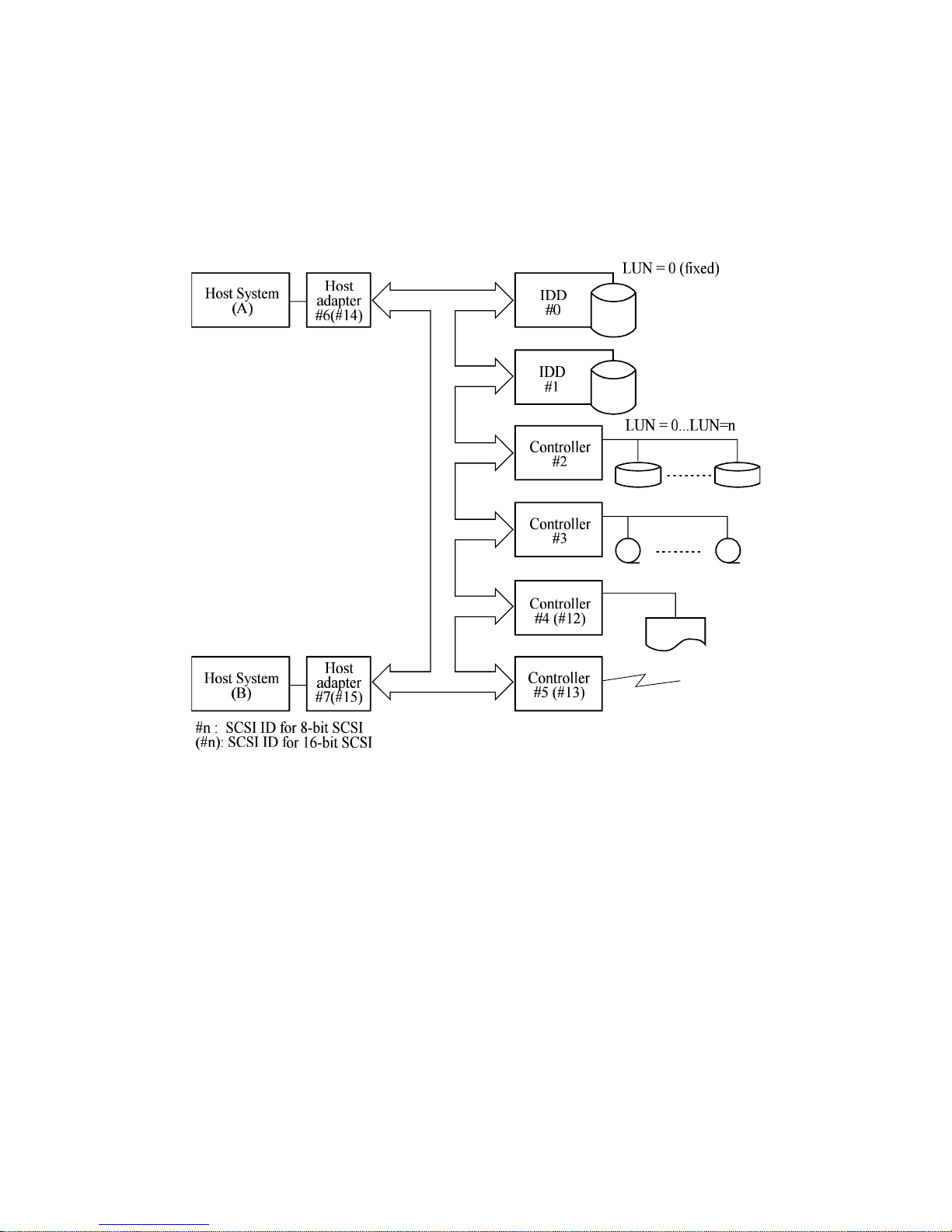
Figure 1.6 shows the system configuration. The IDDs are connected to the SCSI bus of host
systems and are always operated as target. The IDDs perform input/output operation as specified
by SCSI devices which operate as initiator.
Figure 1.6 System configuration
(1) SCSI bus configuration
Up to eight SCSI devices operating as an initiator or a target can be connected to the SCSI bus for
the 8-bit SCSI and up to 16 SCSI devices operating as an initiator or a target can be connected to
the SCSI bus for the 16-bit SCSI in any combination.
For example, the system can be configured as multi-host system on which multiple host computers
that operate as initiator or connected through the SCSI bus.
Using disconnect/reconnect function, concurrent input/output processing is possible on multi-SCSI
devices.
SCSI bus
Page 29

C141-E103-01EN1 - 10
(2) Addressing of peripheral device
Each SCSI device on the bus has its own unique address (SCSI ID:#n in Figure 1.6). For
input/output operation, a peripheral device attached to the SCSI bus that operates as target is
addressed in unit called as logical unit. A unique address (LUN: logical unit number) is assigned
for each logical unit.
The initiator selects one SCSI device by specifying that SCSI ID, then specifies the LUN to select
the peripheral device for input/output operation.
The IDD is constructed so that the whole volume of disk drive is a single logical unit, the
selectable number of SCSI ID and LUN are as follows:
• SCSI ID: 8-bit SCSI:Selectable from 0 to 7 (switch selectable)
16-bit SCSI:Selectable from 0 to 15 (switch selectable)
• LUN: 0 (fixed)
Page 30

C141-E103-01EN 2 - 1
CHAPTER 2 SPECIFICATIONS
2.1 Hardware Specifications
2.2 SCSI Function Specifications
This chapter describes specifications of the IDD and the functional specifications of the SCSI.
2.1 Hardware Specifications
2.1.1 Model name and part number
Each model has a different data format and front panel type when shipped. (See Appendix D for
the model name (type) and product number.)
The data format can be changed by reinitializing with the user's system.
Page 31

C141-E103-01EN2 - 2
2.1.2 Function specifications
Table 2.1 shows the function specifications of the IDD.
Table 2.1 Function specifications
Specification
MAJ3364 series MAJ3182 series MAJ3091 series MAH3182 series MAH3091 series
Formatted capacity/device (*1) 36.4 GB 18.2 GB 9.1 GB 18.2 GB 9.1 GB
Unformatted capacity/device 46.6 GB 23.3 GB 11.7 GB 23.4 GB 11.8 GB
Number of disks 5 3 2 2 1
Number of heads 10 5 3 4 2
Number of cylinders (*2) 14,792 14,808 13,261 17,545 17,686
Formatted capacity/track (B) 188,928 to 293,888 172,032 to 293,888 193,536 to 331,776
Number of rotations min-1 (rpm) 10,025±0.5% 7,200±0.5%
Average latency time 2.993 msec 4.167 msec
Minimum
Average
Maximum
0.6 ms (Read)/0.8 ms (Write)
4.7 ms (Read)/5.2 ms (Write)
11.0 ms (Read)/12.0 ms (Write)
0.6 ms (Read)/0.8 ms (Write)
6.7 ms (Read)/7.3 ms (Write)
14.0 ms (Read)/15.0 ms (Write)
Start time
Stop time
30 s typ. (60 s max.)
30 s typ.
Recording mode 32/34 MEEPRML
Recording density (max) 15.35kb/mm (390 kbpi) 14.96kb/mm (380 kbpi)
Track density (AVE) 748 Track/mm (19,000 TPI)
External dimensions Height
Width
Depth
25.4 mm
101.6 mm
146.0 mm
Weight 0.75 kg 0.6 kg
Power consumption (*5) 12.5 W 10.5 W 9.5 W 6.5 W 6.0 W
Interface Fast SCSI
(Single-Ended)
Cable length: 6 m max
Fast 20 SCSI
(Single-Ended)
Cable length: 3 m max (*6)
Cable length: 1.5 m max (*7)
Fast 80 SCSI
(LVD)
Cable length: 25 m max (*8)
Cable length: 12 m max (*9)
Disk drive 40.5 to 62.4 MB/s 30.0 to 49.5 MB/s
SCSI Synchronous
mode
160 MB/s max.
Logical data block length (*1) 512 to 528 byte (Fixed length)
SCSI command specification ANSI X3.131-1986, ANSI X3.131-1994 and CCS (Rev. 4B) conformity
SPC-2 (T10/1236-D Rev 12), SBC (ANSI NCITS306-199x) command partial support
Data buffer 4 MB FIFO ring buffer
Start/stop time
(*4)
Seek time (*3)
(Read/Write)
Item
Data transfer
rate (*10)
Page 32

C141-E103-01EN 2 - 3
MAJ seriesMAH series
Seek Difference [512 Cyl/div]
10000800060004000
Seek time [ms]
12
10
8
6
4
2
0
0 2000
Seek Difference [512 Cyl/div]
100008000600040000 2000
Seek time [ms]
12
10
8
6
4
2
0
(*1) The formatted capacity can be changed by changing the logical block length and using spare sector
space. See Chapter 3 for the further information.
(*2) The number of user cylinders indicates the max., and includes the alternate cylinder. The number
of user cylinders and alternate cylinders can be specified at format of the IDD.
(*3) The positioning time is as follows:
(*4) The start time is the time from power on or start command to when the IDD is ready, and the stop
time is the time for disks to completely stop from power off or stop command.
(*5) This value indicates at ready mode.
(*6) Up to 4 SCSI devices having capacitance of 25pF or less can use cable length of up to 3.0 m.
(*7) 5 to 8 SCSI devices having capacitance of 25pF or less can use cable length of up to 1.5 m.
(*8) 1 on 1 connection case.
(*9) 1 host, 15 devices case.
(*10) The maximum data transfer rate may be restricted to the response speed of initiator and by
transmission characteristics.
(*11) The terminator power pin (SCSI connector) which supplies power to other terminators is not used.
Page 33

C141-E103-01EN2 - 4
2.1.3 Environmental specifications
Table 2.2 lists environmental and power requirements.
Table 2.2 Environmental/power requirements
Specification
Item
MAJ3364 series MAJ3182 series MAJ3091 series MAH3182 series MAH3091 series
Operating 5 to 50°C
Non-operating –40 to 60°C
DE surface temperature at operating 5 to 55°C
Gradient 15°C/h or less
Operating 20 to 80%RH
Non operating 20 to 80%RH
Packaged (inside of a week) 5 to 90%RH
Maximum wet bulb temperature 29°C (no condensation)
Operating (*3) 0.3 mm (5 to 20Hz)/4.9m/s2 (0.5G) (20 to 300 Hz) or less
Non-operating (*4) 3.1 mm (5 to 20Hz)/49m/s2 (5G) (20 to 300Hz) or less
Packaged 3.1 mm (5 to 20Hz)/49m/s2 (5G) (20 to 300Hz) or less
Operating 196.1m/s2 (20G) (2 ms)
Non-operating 1961.3m/s2 (200G) (2 ms)
Operating –60 m to 3,000 m
Non-operating –60 m to 12,000 m
+12 VDC ±5% Ready (Average) 0.65 A 0.5 A 0.45 A 0.25 A 0.2 A
Peak within
100 µs at spin-up
3.0 A
Random W/R
(about 80 IOPS)
1.3 A 0.8 A 0.7 A 1.0 A
+5 VDC ±5%
(*6)
Ready 0.75A 0.65 A
Random W/R
(about 80 IOPS)
0.6 A
Ripple (*7) +5 V/+12 V 250 mVp-p
(*1) For detail condition, see Section 4.1.
(*2) Vibration applied to the drive is measured at near the mounting screw hole on the frame as much
as possible.
(*3) At random seek write/read and default on retry setting with log sweep vibration.
(*4) At power-off state after installation
Vibration displacement should be less than 2.5 mm.
(*5) Input voltages are specified at the connector.
(*6) The terminator power pin (SCSI connector) which supplies power to other terminators is not used
(See Section 4.3).
(*7) High frequency noise is less than 100 mVp-p.
Altitute
(above sea level)
Shock (*2)
Vibration (*2)
Relative humidity
Temperature (*1)
Power
requirements
Input power (*5)
Page 34

C141-E103-01EN 2 - 5
2.1.4 Error rate
Errors detected during initialization and replaced by alternate block assignments are not included
in the error rate. Data blocks to be accessed should be distributed over the disk medium equally.
(1) Unrecoverable error rate
Errors which cannot be recovered within 63 retries and ECC correction should not exceed 10 per
1015 bits.
CAUTION
Data loss
For MAH and MAJ series, Reed Solomon codes are applied for their
ECC. The sector-data is divided into 4 interleaving sectors, and
ECC is performed in each sector where the maximum number of
errors (up to 5 byte) can be corrected. [Total maximum byte: 5 byte
x 4 ( interleave) = 20 byte]
If the error of read sector keeps allowable error byte number,
correction is performed. However, if error byte exceeds its
allowable number, correction may not be performed properly.
(2) Positioning error rate
Positioning errors which can be recovered by one retry should be 10 or less per 108 seeks.
2.1.5 Reliability
(1) Mean Time Between Failures (MTBF)
MTBF of the IDD during its life time is 1,000,000 hours (operating: 24 hours/day, 7 days/week
average DE surface temperature: 40°C or less).
Note:
The MTBF is defined as:
Operating time (hours) at all field sites
MTBF=
The number of equipment failures from all field sites
Failure of the equipment means failure that requires repair, adjustments, or replacement.
Mishandling by the operator, failures due to bad environmental conditions, power trouble, host
system trouble, cable failures, or other failures not caused by the equipment are not considered.
(2) Mean Time To Repair (MTTR)
Page 35

C141-E103-01EN2 - 6
MTTR is the average time taken by a well-trained service mechanic to diagnose and repair a drive
malfunction. The drive is designed for a MTTR of 30 minutes or less.
(3) Service life
The service life under suitable conditions and treatment is as follows.
The service life is depending on the environment temperature. Therefore, the user must design the
system cabinet so that the average DE surface temperature is as possible as low.
• DE surface temperature: 40°C or less 5 years
• DE surface temperature: 45°C or less 4.5 years
• DE surface temperature: 46°C to 50°C 4 years
• DE surface temperature: 51°C to 55°C 3.5 years
• DE surface temperature: 56°C and more Strengthen cooling power so that DE surface
temperature is 55°C or less.
Even if the IDD is used intermittently, the longest service life is 5 years.
Note:
The "average DE surface temperature" means the average temperature at the DE surface
throughout the year when the IDD is operating.
(4) Data security at power failure
Integrity of the data on the disk is guaranteed against all forms of DC power failure except on
blocks where a write operation is being performed. The above does not applied to formatting
disks or assigning alternate blocks.
Page 36

C141-E103-01EN 2 - 7
2.2 SCSI Function Specifications
Table 2.3 shows the SCSI functions provided with the IDD.
Table 2.3 SCSI function specifications
Item Specification
Single-ended type
Ο
HVD type (High Voltage Differential)
×
LVD type (Low Voltage Differential)
Ο
160/m LVD type (Low Voltage Differential)
Ο
Single-ended type Position where the terminating
resistor is mounted on the PCA
×
Differential type Position where the terminating
resistor is mounted on the PCA
×
Electrical
requirements
(*1)
TERMPWR signal send function
Ο
68 pin P cable connector
Ο
Connector
80 pin SCA2 connector
Ο
Data bus parity (Data bus CRC)
Ο
Bus arbitration function
Ο
Disconnection/reconnection function
Ο
SCSI ID 16-bit SCSI #0 to #15
(Jumper selection)
LUN (logical unit number) #0 fixed
Data transfer
(Synchronous
mode)
8-bit SCSI (Single-Ended type)
(LVD type)
16-bit SCSI (Single-Ended type)
(LVD type)
(160/m LVD type)
Ο 20 MB/s max.
Ο 40 MB/s max.
Ο 40 MB/s max.
Ο 80 MB/s max.
Ο 160 MB/s max.
Data buffer
4 MB (MC/MP) programmable
multi-segment buffer (1 to 32)
Data block length (Logical data length=Physical data length) (*2)
512 to 528 bytes
(Fixed length)
Ο : Provided × : Not provided
(*1) Single-Ended and LVD detect the driver mode by Diffsence signal and automatically change.
(*2) Refer to (12) of Section 1.1.
Addressing
Page 37

This page is intentionally left blank.
Page 38

C141-E103-01EN 3 - 1
CHAPTER 3 DATA FORMAT
3.1 Data Space
3.2 Logical Data Block Addressing
3.3 Defect Management
This chapter explains data space definition, logical data block addressing, and defect management on the
IDD.
3.1 Data Space
The IDD manages the entire data storage area divided into the following three data spaces.
• User space: Storage area for user data
• Internal test space: Reserved area for diagnostic purposes
• System space: Area for exclusive use of IDD itself
The user space allows a user access by specifying data. These space can be accessed with the
logical data block addressing method described in Section 3.2. The internal test space is used by
Read/write test of self-diagnostics test, but user can’t use direct access. The system space is
accessed inside the IDD at power-on or during the execution of a specific command, but the user
cannot directly access the system space.
3.1.1 Cylinder configuration
The IDD allocates cylinders to the user space, Internal test space, and system space. Figure 3.1 is
the cylinder configuration.
Spare areas (alternate areas) for defective sectors are provided in the user space. Several sectors in
the last track of one cylinder and several cylinders (alternate cylinders) in the user space are
allocated as alternate areas according to the user's assignment (MODE SELECT command). See
Subsection 3.1.2 for details.
Page 39

C141-E103-01EN3 - 2
Note: Spare sectors on the last track in each cylinder are not necessarily placed at the end of the track
because of a track skew or a cylinder skew. (Details are explained in Subsection 3.1.3.)
Cylinder 1
n =MAH3182 series: 17,545
MAH3091 series: 17,686
MAJ3364 series: 14,792
MAJ3182 series: 14,808
MAJ3091 series: 13,261
n–1
n–2
Cylinder 0
Cylinder –59
to
Cylinder –4
User space
System space
Internal test space
Cylinder –70
to
Cylinder –63
•
Primary Cylinder 0
to
Primary Cylinder (n–1)
Spare sector for each cylinder
SA1
SA56
Internal test cylinder
~~
~~
~~
~~
• •
•
•
~~
n
Figure 3.1 Cylinder configuration
Apart from the above logical configuration, the IDD intends to increase the storage capacity by
dividing all cylinders into several zones and changing a recording density of each zone. Tables 3.1
to 3.3 show the zone layout and the track capacity.
Page 40

C141-E103-01EN 3 - 3
Table 3.1 Zone layout and track capacity (MAJ3364 series/MAJ3182 series)
Zone 0 1 2 3 4 5 6 7
Cylinder 0 to 749 750 to
1,499
1,500 to
2,179
2,180 to
2,859
2,860 to
4,039
4,040 to
5,034
5,035 to
6,029
6,030 to
7,229
Byte/track 373,107 373,107 369,157 364,070 353,177 345,696 337,915 325,108
Sector/track 574 574 568 560 546 532 518 504
Zone 8 9 10 11 12 13 14 15
Cylinder 7,230 to
8,389
8,390 to
9,589
9,590 to
10,439
10,440 to
11,199
11,200 to
12,369
12,370 to
13,199
13,200 to
13,912
13,913 to
14,791
*1 (14,807)
Byte/track 313,736 299,671 291,412 282,853 271,003 260,409 251,851 241,496
Sector/track 483 462 448 434 420 399 385 369
(*1) The value given in parenthesis is for MAJ3182 series.
Note: When the logical data block length is 512 bytes, the sector/track capacity indicates above amount.
Table 3.2 Zone layout and track capacity (MAJ3091 series)
Zone 0 1 2 3 4 5 6
Cylinder 0 to 579 580 to
1,339
1,340 to
2,249
2,250 to
3,219
3,220 to
4,554
4,555 to
5,489
5,490 to
6,654
Byte/track 373,107 364,069 353,177 341,387 325,108 313,736 299,671
Sector/track 574 560 546 525 504 483 462
Zone 7 8 9 10 11 12 13
Cylinder 6,655 to
7,719
7,720 to
8,999
9,000 to
9,879
9,880 to
11,099
11,100 to
11,789
11,790 to
12,499
12,500 to
13,260
Byte/track 286,683 271,002 260,409 245,566 237,307 228,749 219,950
Sector/track 441 420 399 378 364 350 336
Note: When the logical data block length is 512 bytes, the sector/track capacity indicates above amount.
Page 41

C141-E103-01EN3 - 4
Table 3.3 Zone layout and track capacity (MAH series)
Zone 0 1 2 3 4 5 6 7
Cylinder 0 to 859 860 to
1,959
1,960 to
2,639
2,640 to
3,969
3,970 to
5,149
5,150 to
6,429
6,430 to
7,759
7,760 to
8,689
Byte/track 418,715 404,500 397,667 386,000 375,667 363,750 348,917 341,083
Sector/track 648 621 612 594 576 558 540 522
Zone 8 9 10 11 12 13 14 15
Cylinder 8,690 to
10,019
10,020 to
11,249
11,250 to
12,299
12,300 to
13,319
13,320 to
14,649
14,650 to
15,379
15,380 to
16,499
16,500 to
17,544
*1 (17,685)
Byte/track 328,667 316,417 306,083 295,166 278,583 271,750 259,333 246,333
Sector/track 504 486 468 450 432 414 396 378
(*1) The value given in parenthesis is for MAH3091 series.
Note: When the logical data block length is 512 bytes, the sector/track capacity indicates above amount.
(1) User space
The user space is a storage area for user data. The data format on the user space (the length of data
block and the number of data blocks) can be specified with the MODE SELECT or MODE
SELECT EXTENDED command.
The default value of cylinders in the user space is MAH3182 series = 17545, MAH3091 series =
17,686, MAJ3364 series = 14,792, MAJ3182 series = 14,808 and MAJ3091 series = 13,261.
These also equal the maximum cylinders number for each series. The user can also specify the
number of logical data blocks to be placed in the user space with the MODE SELECT or MODE
SELECT EXTENDED command. When the number of logical data blocks is specified, as many
cylinders as required to place the specified data blocks are allocated in the user space.
A number staring with 0 is assigned to each cylinder required in the user space in ascending order.
If the number of cylinders do not reach the maximum, the rest of the cylinders will not be used.
Always one alternate cylinders can be established in the user space. Alternate cylinders will be
used for alternate blocks when primary cylinders in the user space are used up. See Subsections
3.1.2 and 3.3.2 for details.
(2) Internal test space
The Internal test space is an area for diagnostic purposes only and its data block length is always
512KByte. The Internal test space consists of 8 cylinders and outer-host cylinder is always
assigned. The user cannot change the number of cylinders in the Internal test space or their
positions.
Page 42

C141-E103-01EN 3 - 5
(3) System space
The system space is an area for exclusive use of the IDD itself and the following information are
recorded. The length of the data block is always 512 bytes.
• Defect list (P list and G list)
• MODE SELECT parameter (saved value)
• Statistical information (log data)
• Controller control information
The above information are duplicated in several different locations for safety.
Note:
The system space is also called SA space.
3.1.2 Alternate spare area
The alternate spare area is provided in the last track of each primary cylinder in the user space, and
in the last track of the cylinder and the alternate cylinder.
The spare area in each cylinder is placed at the end of the last track as shown in Figure 3.2. These
spare sectors are located in the end of the track logically, not necessarily located at the end
physically because of track skew or cylinder skew. (Details are explained on Subsection 3.1.3.)
Size can be specified by the MODE SELECT command.
The number of spare sectors per cylinder can be specified exceeding 32. The default value of
number of 9 space sectors per cylinder is 20.
Figure 3.2 Spare area in cylinders
An alternate cylinder is used when spare sectors in a cylinder are used up or 0 is specified as the
number of spare sectors in a cylinder. 1 cylinder at the end of the user space are allocated as
alternate cylinders as shown in Figure 3.3.
Page 43

C141-E103-01EN3 - 6
The user space and the CE space share the alternate cylinders.
Figure 3.3 Alternate cylinder
Note:
Zero cannot be specified for both the number of spare sectors in each cylinder and the number
of alternate cylinders.
3.1.3 Track format
(1) Physical sector allocation
Figure 3.4 shows the allocation of the physical sectors in a track. The length in bytes of each
physical sector and the number of sectors per track vary depending on the logical data block
length. The unused area (G4) exists at the end of the track in formats with most logical data block
lengths.
The interval of the sector pulse (length of the physical sector) is decided by multiple of 20MHz
free running frequency. This clock is not equal to the interval of the byte clock for each zone.
Therefore, the physical sector length cannot be described with a byte length.
J
Figure 3.4 Track format
Page 44

C141-E103-01EN 3 - 7
(2) Track skew and cylinder skew
To avoid waiting for one turn involved in head and cylinder switching, the first logical data block
in each track is shifted by the number of sectors (track skew and cylinder skew) corresponding to
the switching time. Figure 3.5 shows how the data block is allocated in each track.
At the head switching location in a cylinder, the first logical data block in track t + 1 is allocated at
the sector position which locates the track skew behind the sector position of the last logical data
block sector in track t.
At the cylinder switching location, like the head switching location, the first logical data block in a
cylinder is allocated at the sector position which locates the cylinder skew behind the last logical
sector position in the preceding cylinder. The last logical sector in the cylinder is allocated when
formatting, and is an unused spare sector.
Figure 3.5 Track skew/cylinder skew
The number of physical sectors (track skew factor and cylinder skew factor) corresponding to the
skew time varies depending on the logical data block length because the track skew and the
cylinder skew are managed for individual sectors. The IDD automatically determines appropriate
values for the track skew factor and the cylinder skew factor according to the specified logical data
block length. The value can be read out by the MODE SENSE or MODE SENSE EXTENDED
command after the track has been formatted.
Page 45

C141-E103-01EN3 - 8
3.1.4 Sector format
Each sector on the track consists of an ID field, a data field, and a gap field which separates them.
Figure 3.6 gives sector format examples.
SCT
PAD
SM1
PLO
SyncG1
SCT
G1 4 bytes
G2 11 bytes
G3 8 bytes
PLO Sync 30 bytes
SM1 4 bytes
SM2 2 bytes
BCRC 4 bytes
ECC 40 bytes
PAD 6 bytes
DATA1 20 bytes
DATA2 492 bytes
DATA3
n bytes (0≤n≤472,
n is a multiple of 4.)
DATA4 (472 – n) bytes
G2
DATA1 SM2 BCRCDATA2 ECC
SCT
PAD
SM1
PLO
Sync
G1
SCT
G3
DATA1 SM2 DATA3
PAD
G2
SM1
PLO
SyncG1
DATA1 SM2 DATA4
Servo
BCRC ECC
Figure 3.6 Sector format
Each sector on the track consists of the following fields:
(1) Gaps (G1, G2, G3)
The gap length at the time of formatting (initializing) is listed in Figure 3.6. No pattern is written
on the gap field.
(2) PLO Sync
In this field, pattern X'00' in the length in bytes listed in Figure 3.6 is written.
(3) Sync Mark (SM1, SM2)
In this field, special pattern in the length in bytes listed in Figure 3.6 is written. This special
pattern indicates the beginning of the data field.
Page 46

C141-E103-01EN 3 - 9
(4) Data field (DATA1-DATA4)
User data is stored in the data field of the sector. The length of the data field is equal to that of the
logical data block which is specified with a parameter in the MODE SELECT command. Any
even number between 512 and 528 bytes can be specified as the length.
(5) BCRC
It is a 4-byte error detection code. Errors in the ID field. Single burst errors with lengths of up to
32 bits for each logical block can be detected.
(6) ECC
This is the 40-byte code that allows detection and correction of errors in the data field, which is
capable of correcting the single burst error up to 160 bits max. on the fly.
(7) PAD
A specified length of x‘00’ pattern shown in Figure 3.6 is written in this field. This field includes
the variation by rotation and circuit delay till reading/writing.
Page 47

C141-E103-01EN3 - 10
3.1.5 Format capacity
The size of the usable area for storing user data on the IDD (format capacity) varies according to
the logical data block or the size of the spare sector area. Table 3.4 lists examples of the format
capacity when the typical logical data block length and the default spare area are used. The
following is the general formula to calculate the format capacity.
[Number of sectors of each zone] = [number of sectors per track × number of tracks (heads) –
number of alternate spare sectors per cylinder] × [number of cylinders in the zone]
[Formatted capacity] = [total of sectors of all zones] – [number of sectors per track in last zone ×
number of tracks (heads) × number of alternate cylinders] ÷ [number of physical sectors in logical
block] × [logical data block length]
The following formula must be used when the number of logical data blocks are specified with the
parameter in the MODE SELECT or MODE SELECT EXTENDED command.
[Format capacity] = [logical data block length] × [number of logical data blocks]
The logical data block length, the maximum logical block address, and the number of the logical
data blocks can be read out by a READ CAPACITY, MODE SENSE, or MODE SENSE
EXTENDED command after initializing the disk medium.
Table 3.4 Format capacity
Model Data heads Data block length User blocks Format capacity (GB)
MAH3182 series 4 35,701,260 18.28
MAH3091 series 2 17,850,264 9.14
MAJ3364 series 10 512 71,390,320 36.55
MAJ3182 series 5 35,694,904 18.28
MAJ3091 series 3 17,847,486 9.14
Note:
Total number of spare sectors is calculated by adding the number of spare sectors in each
primary cylinder and the number of sectors in the alternate cylinders.
Page 48

C141-E103-01EN 3 - 11
3.2 Logical Data Block Addressing
Independently of the physical structure of the disk drive, the IDD adopts the logical data block
addressing as a data access method on the disk medium. The IDD relates a logical data block
address to each physical sector at formatting. Data on the disk medium is accessed in logical data
block units. The INIT specifies the data to be accessed using the logical data block address of that
data.
The logical data block addressing is a function whereby individual data blocks are given addresses
of serial binaries in each drive.
(1) Block address of user space
The logical data block address number is consecutively assigned to all of the data blocks in the
user space starting with 0 to the first data block.
The IDD treats sector 0, track 0, cylinder 0 as the first logical data block. The data block is
allocated in ascending order of addresses in the following sequence (refer to Figure 3.5):
1) Numbers are assigned in ascending order to all sectors in the same track.
2) By following step 1), numbers are assigned in ascending order of tracks to all sectors in each
track in the same cylinder except the last track.
3) By following step 1), numbers are assigned to all sectors in the last track except the spare
sectors.
4) After completing steps 1) through 3) for the same cylinder, this allocation is repeated from
track 0 in the next cylinder and on to the last cylinder (cylinder p-q in Figure 3.1) except for
the alternate cylinders in ascending order of cylinder numbers.
When the logical data block is allocated, some sectors (track skew and cylinder skew) shown in
Figure 3.5 are provided to avoid waiting for one turn involving head and cylinder switching at the
location where the track or the cylinder is physically switched.
See Subsection 3.3.2 for defective/alternate block treatment and the logical data block allocation
method in case of defective sectors exist on the disk.
(2) Alternate area
Alternate areas in the user space (spare sectors in the cylinder and alternate cylinders) are not
included in the above logical data block addresses. Access to sectors which are allocated as an
alternate block in the alternate area is made automatically by means of IDD sector slip treatment or
alternate block treatment (explained in Subsection 3.3.2), so the user does not have to worry about
accessing the alternate area. The user cannot access with specifying the data block on the alternate
area explicitly.
Page 49

C141-E103-01EN3 - 12
3.3 Defect Management
3.3.1 Defect list
Information of the defect location on the disk is managed by the defect list. The following are
defect lists which the IDD manages.
• P list (Primary defect list): This list consists of defect location information available at the
disk drive shipment and is recorded in a system space. The defects in this list are permanent,
so the INIT must execute the alternate block allocation using this list when initializing the disk.
• D list (Data defect list): This list consists of defect location information specified in a
FORMAT UNIT command by the INIT at the initialization of the disk. This information is
recorded in the system space of the disk drive as the G list. To execute the alternate block
allocation, the FORMAT UNIT command must be specified.
• G list (Growth defect list): This list consists of defective logical data block location
information specified in a REASSIGN BLOCKS command by the INIT, information on
defective logical data blocks assigned alternate blocks by means of IDD automatic alternate
block allocation, information specified as the D list, and information generated as the C list.
They are recorded in the system space on the disk drive.
The INIT can read out the contents of the P and G lists by the READ DEFECT DATA command.
3.3.2 Alternate block allocation
The alternate data block is allocated to a defective data block (= sectors) in defective sector units
by means of the defect management method inside the IDD.
The INIT can access all logical data blocks in the user space, as long as there is no error.
Spare sectors to which alternate blocks are allocated can be provided in either "spare sectors in a
cylinder" or "alternate cylinders". See Subsection 3.1.2 for details.
The INIT can specify the size and area for spare sectors by the MODE SELECT command at the
time of the initialization of the disk.
Both of the following are applicable to the alternate block allocation.
• Sector slip treatment: Defective sectors are skipped and the logical data block corresponding
to those sectors is allocated to the next physical sectors. This treatment is made on the same
cylinder as the defective sector's and is effective until all spare sectors in that cylinder are used
up.
• Alternate sector treatment: The logical data block corresponding to defective sectors is
allocated to unused spare sectors in the same cylinder or unused spare sectors in the alternate
cylinder.
Page 50

C141-E103-01EN 3 - 13
The alternate block allocation is executed by the FORMAT UNIT command, the REASSIGN
BLOCKS command, or the automatic alternate block allocation. Refer to OEM Manual–SCSI
Logical Specifications–for details of specifications on these commands. The logical data block is
allocated to the next physically continued sectors after the above sector slip treatment is made. On
the other hand, the logical data block is allocated to spare sectors which are not physically
consecutive to the adjacent logical data blocks. If a command which processes several logical data
blocks is specified, the IDD processes those blocks in ascending order of logical data block.
(1) Alternate block allocation during FORMAT UNIT command execution
When the FORMAT UNIT command is specified, the allocation of the alternate block to those
defective sectors included in the specified lists (P, G, or D) is continued until all spare sectors in
the same cylinder are used up. When they are used up, unused spare sectors in the alternate
cylinder are allocated to the subsequent sectors in the cylinder by means of alternate sector
treatment. Figure 3.7 is examples of the alternate block allocation during the FORMAT UNIT
command execution.
Page 51

C141-E103-01EN3 - 14
Figure 3.7 Alternate block allocation by FORMAT UNIT command
If the data block verifying operation (certification) is not permitted (DCRT flag = 0) in the
FORMAT UNIT command, the IDD checks all initialized logical data blocks by reading them out
after the above alternate block allocation is made to initialize (format) the disk. If a defective data
block is detected during the check, the IDD allocates the alternate block to the defective data
block. This alternate block allocation is made by means of alternate sector treatment only like
processing by the REASSIGN BLOCKS command even if unused spare sectors exists in the same
cylinder.
: Unused spare sector
: Defective sector
: n represents a logical data block number
Page 52

C141-E103-01EN 3 - 15
(2) Alternate block allocation by REASSIGN BLOCKS command
When the REASSIGN BLOCKS command is specified, the alternate block is allocated to the
defective logical data block specified by the initiator by means of alternate sector treatment. If
there are unused spare sectors in the same cylinder as the specified defective logical data block, the
alternate block is allocated to these unused spare sectors. However, the alternate block is allocated
to unused spare sectors in the alternate cylinder when all spare sectors in the cylinder are used up.
Figure 3.8 is examples of the alternate block allocation by the REASSIGN BLOCKS command.
Figure 3.8 Alternate block allocation by REASSIGN BLOCKS command
: Unused spare sector
: Defective sector
: n represents a logical data block number
Page 53

C141-E103-01EN3 - 16
(3) Automatic alternate block allocation
• Automatic alternate block allocation at read operation
If the ARRE flag in the MODE SELECT parameter permits the automatic alternate block
allocation, the IDD automatically executes the alternate block allocation and data duplication on
the defective data block detected during the READ or READ EXTENDED command. This
allocation method is the same as with the REASSIGN BLOCKS command (alternate sector
treatment).
• Automatic alternate block allocation at write operation
If the AWRE flag in the MODE SELECT parameter permits the automatic alternate block
allocation, the IDD executes reassign processing to all the existing sectors in the servo frame where
offtrack error occurred during WRITE/WRITE EXTENDED command processing and in the next
servo frame. After completing reassignment, WRITE/WRITE EXTENDED command processing
is successively executed for the following sectors.
IMPORTANT
Automatic alternate block allocation is made only once during the
execution of one command. If second defective block is detected, the
alternate block assignment processing for the first defective block is
executed but the alternate block assignment processing for the
second one is not executed and the command being executed
terminates. However, the initiator can recover the twice error by
issuing the same command again.
When an error is detected in a data block in the data area, recovery
data is rewritten and verified in automatic alternate block allocation
during the execution of the READ or READ EXTENDED command.
Alternate block allocation will not be made for the data block if
recovery is successful.
Example: Even if the data error which is recoverable by the WRITE
LONG command is simulated, automatic alternate block
allocation will not be made for the data block.
Page 54

C141-E103-01EN 4 - 1
CHAPTER 4 INSTALLATION REQUIREMENTS
4.1 Mounting Requirements
4.2 Power Supply Requirements
4.3 Connection Requirements
This chapter describes the environmental, mounting, power supply, and connection requirements.
4.1 Mounting Requirements
4.1.1 External dimensions
Figures 4.1 to 4.4 show the external dimensions of the IDD and the positions of the holes for the
IDD mounting screws.
Note:
Dimensions are in mm.
Page 55

C141-E103-01EN4 - 2
3.175 ± 0.25
Figure 4.1 External dimensions (MAH series MC model)
Page 56

)LJXUH ([WHUQDOGLPHQVLRQV0$+VHULHV03PRGHO
&((1
Page 57

C141-E103-01EN4 - 4
3.175 ± 0.25
Figure 4.3 External dimensions (MAJ series MC model)
Page 58

)LJXUH ([WHUQDOGLPHQVLRQV0$-VHULHV03PRGHO
&((1
Page 59

C141-E103-01EN4 - 6
4.1.2 Mounting
The permissible directions of the IDD are shown in Figure 4.7, and the tolerance of the angle is
±5° from the horizontal plane.
Figure 4.5 IDD directions
4.1.3 Notes on mounting
(1) Mounting frame structure
Special attention must be given to mount the IDD disk enclosure (DE) as follows.
a) Use the frame with an embossed structure, or the like. Mount the IDD with making a gap
of 2.5 mm or more between the IDD and the frame of the system.
b) As shown in Figure 4.6, the inward projection of the screw from the IDD frame wall at the
corner must be 4 mm or less.
c) Tightening torque of screw must be secured with 0.59N·m (6kgf·cm).
d) Impact caused by the electric driver must be within the device specifications.
e) Must be handled on an anti-static mat.
Direction of
gravity
(a) Horizontal –1 (b) Horizontal –2
(c) Vertical –1
(d) Vertical –2 (e) Upright mounting –1 (f) Upright mounting –2
Page 60

C141-E103-01EN 4 - 7
Figure 4.6 Mounting frame structure
(2) Limitation of side-mounting
Mount the IDD using the 4 screw holes at the both ends on the both sides as shown in Figure 4.7.
Do not use the center hole by itself.
In case of using the center hole, it must be used in combination with 2 holes on both ends.
(Total 6 screws for 6 holes enclosed)
Figure 4.7 Limitation of side-mounting
(3) Limitation of bottom-mounting
Use all 4 mounting holes on the bottom face.
4
3
2
1
Use four holes (No.1-4) to mount.
Holes for
mounting screw.
Holes for mounting screw.
Do not use these holes
Page 61

C141-E103-01EN4 - 8
(4) Environmental temperature
Temperature condition at installed in a cabinet is indicated with ambient temperature measured 3
cm from the disk drive. At designing the system cabinet, consider following points.
• Make a suitable air flow so that the DE surface temperature does not exceed 55°C.
• Cool the PCA side especially with air circulation inside the cabinet. Confirm the cooling effect
by measuring temperature of specific ICs and the DE. These measurement results should be
within a criteria listed in Table 4.1.
Table 4.1 Surface temperature check point
No. Measurement point Criteria
1 Center of DE cover 55°C
2 Read channel LSI 83°C
3 VCM/SPM Driver 75°C
4 HDC 85°C
Figure 4.8 Surface temperature measurement points
1
1
1
3
2
4
4
4
3
2
2
3
MAJ3364 Series
MAJ3182, MAJ3091 Series
MAH Series
Page 62

C141-E103-01EN 4 - 9
(4) Service clearance area
The service clearance area, or the sides which must allow access to the IDD for installation or
maintenance, is shown in Figures 4.9.
Figure 4.9 Service clearance area
(5) External magnetic field
The drive should not be installed near the ferromagnetic body like a speaker to avoid the influence
of the external magnetic field.
(6) Leak magnetic flux
The IDD uses a high performance magnet to achieve a high speed seek. Therefore, a leak
magnetic flux at surface of the IDD is large. Mount the IDD so that the leak magnetic flux does
not affect to near equipment.
(7) Others
A hole or screw portion as shown in Figure 4.10 is used for adjusting air pressure balance between
inside and outside the DE. Do not fill with a seal or label.
Seals on the DE prevent the DE inside from the dust. Do not damage or peel off labels.
[Surface P’]
• Setting terminal
• External operator panel connector
• Spindle sync connector
[Surface R]
• Hole for mounting screw
[Surface Q]
• Hole for mounting screw
[Surface P]
• Cable connection
Page 63

C141-E103-01EN4 - 10
MAJ series
Figure 4.10 Air pressure adjustment hole
Air pressure adjustment hole
Page 64

C141-E103-01EN 4 - 11
4.2 Power Supply Requirements
(1) Allowable input voltage and current
The power supply input voltage measured at the power supply connector pin of the IDD (receiving
end) must satisfy the requirement given in Subsection 2.1.3. (For other requirements, see Items (4)
and (5) below.)
(2) Current waveform (reference)
Figure 4.11 shows the waveform of +12 VDC.
MAJ3364 series MAJ3182 series MAJ3091 series
MAH3182 series MAH3091 series
Figure 4.11 Current waveform (+12 VDC)
(3) Power on/off sequence
a) The order of the power on/off sequence of +5 VDC and +12 VDC, supplied to the IDD, does
not matter.
b) In a system which uses the terminating resistor power supply signal (TERMPWR) on the SCSI
bus, the requirements for +5 VDC given in Figure 4.12 must be satisfied between the IDD and
at least one of the SCSI devices supplying power to that signal.
Page 65

C141-E103-01EN4 - 12
Figure 4.12 Power on/off sequence (1)
c) In a system which does not use the terminating resistor power supply signal (TERMPWR) on
the SCSI bus, the requirements for +5 VDC given in Figure 4.13 must be satisfied between the
IDD and the SCSI device with the terminating resistor circuit.
Figure 4.13 Power on/off sequence (2)
d) Between the IDD and other SCSI devices on the SCSI bus, the +5 VDC power on/off sequence
is as follows:
• In a system with its all SCSI devices designed to prevent noise from leaking to the SCSI
bus when power is turned on or off, the power sequence does not matter if the
requirement in b) or c) is satisfied.
• In a system containing an SCSI device which is not designed to prevent noise from
leaking to the SCSI bus, the requirement given in Figure 4.14 must be satisfied between
that SCSI device and the IDD.
Figure 4.14 Power on/off sequence (3)
SCSI devices
without noise
leaking designed
SCSI devices with
the terminating
resistor
Page 66

C141-E103-01EN 4 - 13
(4) Sequential starting of spindle motors
After power is turned on to the IDD, a large amount of current flows in the +12 VDC line when the
spindle motor rotation starts. Therefore, if more than one IDD is used, the spindle motors should
be started sequentially using one of the following procedures to prevent overload of the power
supply unit. For how to set a spindle motor start control mode, see Subsection 5.3.2.
a) Issue START/STOP commands at more than 12-second intervals to start the spindle motors.
For details of this command specification, refer to SCSI Logical Interface Specifications.
b) Turn on the +12 VDC power in the power supply unit at more than 12-second intervals to start
the spindle motors sequentially.
(5) Power supply to SCSI terminating resistor
If power for the terminating resistor is supplied from the IDD to other SCSI devices through the
SCSI bus, the current-carrying capacity of the +5 VDC power supply line to the IDD must be
designed with considering of an increase of up to 200 mA.
A method of power supply to the terminating resistor is selected with a setting terminal on the
IDD. See Subsection 5.3.2 for this selection.
For the electrical condition of supplying power to the terminating resistor, refer to Subsection 1.4.2
in SCSI Physical Interface Specifications.
(6) Noise filter
To eliminate AC line noise, a noise filter should be installed at the AC input terminal on the IDD
power supply unit. The specification of this noise filter is as follows:
• Attenuation: 40 dB or more at 10 MHz
• Circuit construction: T-configuration as shown in Figure 4.15 is recommended.
Figure 4.15 AC noise filter (recommended)
Page 67

C141-E103-01EN4 - 14
4.3 Connection Requirements
4.3.1 68 pin connector 16-bit SCSI model (MP model)
(1) Connectors
Figures 4.16 show the locations of connectors and terminals on the 68 pin connector type 16-bit
SCSI (MP) model.
• Power supply connector
• SCSI connector
• External operator panel connector
Figure 4.16 Connectors and terminals location (MP model)
SCSI connector
(CN1)
External operator panel
connector (CN2)
External operator
panel connector
(CN1)
Power supply
connector
(CN1)
External operator panel
connector (CN2)
Power supply
connector
(CN1)
External operator
panel connector
(CN1)
SCSI connector
(CN1)
MAH series
MAJ series
Page 68

C141-E103-01EN 4 - 15
(2) SCSI connector and power supply connector
a. 16-bit SCSI
The connector for the SCSI bus is an unshielded P connector conforming to SCSI-3 type which
has two 34-pin rows spaced 1.27 mm (0.05 inch) apart. Figure 4.17 shows the SCSI
connector. See Section C.2 in Appendix C for the signal assignments on the SCSI connector.
For details on the physical/electrical requirements of the interface signals, refer to Sections 1.3
and 1.4 in the SCSI Physical Interface Specifications.
Figure 4.17 16-bit SCSI interface connector
b. Power supply connector
Figure 4.18 shows the shape and the terminal arrangement of the output connector of DC
power supply.
Figure 4.18 Power supply connector (16-bit SCSI model)
The tolerance is ±0.127 mm (0.005 inch) unless otherwise specified
Page 69

C141-E103-01EN4 - 16
(3) SG terminal
The IDD is not provided with an SG terminal (fasten tab) for DC grounding. Therefore, when
connecting SG and FG in the system, use the +5 VDC RETURN (ground) inside the power supply
connector as the SG on the power supply side.
(4) Connector for external operator panel
• Connector for 16-bit SCSI external operator panel
CN1 provides connector for the external operator panel other than the SCSI bus as shown in
Figure 4.19. Also, a connector for the external operator panel are provided on the IDD as
shown in Figure 4.20. This allows connection of an external LED on the front panel, and an
SCSI ID setting switch. For the recommended circuit of the external operator panel, see
Subsection 4.3.4.
Figure 4.19 External operator panel connector (CN1)
Pin Signal
A1 –ID0
A2 –Fault LED
A3 –ID1
A4 (Reserved)
A5 –ID2
A6 (Reserved)
A7 –ID3
A8 –LED
A9 OPEN
A10 GND
A11 +5 V
A12 –WTP
Page 70

C141-E103-01EN 4 - 17
Figure 4.20 External operator panel connector (CN2)
Page 71

C141-E103-01EN4 - 18
(5) External operator panel connector Signals
a. 16-bit SCSI –ID3, –ID2, –ID1, –ID0: Input signals (CN1-A1, A3, A5, A7 pin and CN2-02,
04, 06, 08 pin)
These signals are used for providing switches to set the SCSI ID of the IDD externally. Figure
4.21 shows the electrical requirements. For the recommended circuit examples, see Subsection
4.3.4.
Figure 4.21 16-bit SCSI ID external input
Page 72

C141-E103-01EN 4 - 19
b. –Fault LED: Output signal (CN1-A2 pin)
The IDD indicates that the write-protect status is in effect (CN1-A12 is connected to the GND, or the
CN2-9 and CN2-10 are short-circuited.) A signal for driving the LED is output.
74LS06 or equivalent
150
Ω
NC1-A2
(IDD)
IMPORTANT
This signal is temporarily driven at the GND level when the micro
program reads the SCSI ID immediately after the power supply to
the IDD has been switched on (it is possible to set up the SCSI ID by
short circuiting CN1-A1 and CN1-A2.)
c. CN1-A4, CN1-A6 (reserved)
These pins are temporarily driven at the GND level when the micro program reads the SCSI ID
immediately after the power supply to the IDD has been switched on (it is possible to set up the SCSI
ID by short circuiting CN1-A3 and CN1-A4, and CN1-A5 and CN1-A6.)
These pins get high impedance status except above.
d. –LED and LED (V): Output signals (CN1-A8 pin and CN2-21, 22 pin)
These signals actuate the external LED as same as LED on the front panel of the disk drive.
The electrical requirements are given in Figure 4.22.
IMPORTANT
1. The external LED is identical in indication to the LED on the front of the
IDD. The meaning of indication can be selected with the CHANGE
DEFINITION command. For details of command, refer to SCSI Logical
Interface Specifications.
2. Any load other than the external LED (see Subsection 4.3.5) should not
be connected to the LED (V) and –LED terminals.
3. This signal is temporarily driven at the GND level when the micro
program reads the SCSI ID immediately after the power supply to the
IDD has been switched on (it is possible to set up the SCSI ID by short
circuiting CN1-A7 and CN1-A8.)
Page 73

C141-E103-01EN4 - 20
Figure 4.22 Output signal for external LED
e. –WTP: Input signal (CN1-A12 and CN2-9, 10 pin)
By connecting the CN1-A12 and CN2-10 pins to the GND, writing operations into the IDD
disc media are set to disable.
Page 74

C141-E103-01EN 4 - 21
(6) Cable connection requirements
The requirements for cable connection between the IDD, host system, and power supply unit are
given in Figure 4.23. Recommended components for connection are listed in Table 4.2.
Figure 4.23 SCSI cables connection
External operator panel
(example)
Page 75

C141-E103-01EN4 - 22
4.3.2 SCA2 type SCSI model (MC model)
(1) Connectors
Figure 4.24 shows the locations of connectors and terminals on the SCA2 type SCSI model. SCSI
connector (including power supply connector)
Figure 4.24 Connectors and terminals location of MC model
SCSI connector (CN1)
External operator panel
connector (CN2)
External operator panel
connector (CN2)
SCSI connector (CN1)
Page 76

C141-E103-01EN 4 - 23
(2) SCSI connector and power supply connector
a. SCA type SCSI
The connector for the SCSI bus is an unshielded SCA-2 connector conforming to SCSI-3 type
which has two 40-pin rows spaced 1.27 mm (0.05 inch) apart. Figure 4.25 shows the SCSI
connector. See Section C.5 in Appendix C for signal assignments on the connector.
For details on the physical/electrical requirements of the interface signals, refer to Sections 1.3
and 1.4 in SCSI Physical Interface Specifications.
Figure 4.25 SCA2 type SCSI connector
Page 77

C141-E103-01EN4 - 24
(3) Connector for external operator panel
• Connector external operator panel
A connector for the external operator panel are provided on the IDD as shown in Figure 4.26.
This allows to place externally LED on the front panel, or an SCSI ID setting switch.
Figure 4.26 External operator panel connector (CN2)
Page 78

C141-E103-01EN 4 - 25
(4) External operator panel connector Signals
a. 16-bit SCSI –ID3, –ID2, –ID1, –ID0: Input signals (CN-2-02, 04, 06, 08 pin)
These signals are used for providing switches to set the SCSI ID of the IDD externally. Figure
4.27 shows the electrical requirements.
Figure 4.27 16-bit SCSI ID external input
CN2-02
CN2-04
CN2-06
(IDD)
CN2-08
Page 79

C141-E103-01EN4 - 26
b. –WTP: Input signal (CN2-9, 10 pin)
By connecting the CN2-10 pins to the GND, writing operations into the IDD disc media are set
to disable.
4.3.3 Cable connector requirements
Table 4.2 lists the recommended components cable connection.
Table 4.2 Recommended components for connection
Applicable
model
Name Par number Manufacturer
Reference
(Figures 4.25
and 4.30)
Cable socket
(closed-end type)
786090-7 AMPSCSI cable (CN1)
Signal cable — —
S1
Cable socket
housing
1-480424-0 AMP
Contact 170121-4 AMP
Power supply cable
(CN1)
Cable AWG20
S2
Cable socket
housing
FCN-723J012/2M Fujitsu Limited
Contact FCN-723J-G/AM Fujitsu Limited
External operator
panel (CN1)
Cable AWG26 to 34
S3
Cable socket
housing
FCN-723J016/2M Fujitsu Limited
Contact FCN-723J-G/AM Fujitsu Limited
MP
External operator
panel (CN2)
Cable AWG28
S4
MC SCSI connector
(CN1)
Connector 787311-1 AMP
(1) SCSI cable
See Section 1.3, “Physical Requirements”, and Section 1.4, “Electrical Requirements”, in SCSI
Physical Interface Specifications.
(2) Power cable
IDDs must be star-connected to the DC power supply (one to one connection) to reduce the
influence of load variations.
(3) DC ground
The DC ground cable must always be connected to the IDD because no fasten terminal dedicated
to SG is provided with the IDD. Therefore, when SG and FG are connected in the system, it is
necessary to connect SG and FG at the power supply or to connect SG of the power supply to FG
of the system.
Page 80

C141-E103-01EN 4 - 27
(4) External operator panel
The external operator panel is installed only when required for the system. When connection is not
required, leave open the following pins in the external operator panel connector of the IDD : Pins
21, 22 and pins 01 through 08 in CN2 and pins A1 through A12 in CN1.
4.3.4 External operator panel
A recommended circuit of the external operator panel is shown in Figure 4.28. Since the external
operator panel is not provided as an option, this panel must be fabricated at the user site referring
to the recommendation if necessary.
(MP)
Figure 4.28 External operator panel circuit example
IMPORTANT
Do not connect the external LED to both CN1 and CN2. Connect it
to either of them.
Page 81

This page is intentionally left blank.
Page 82

C141-E103-01EN 5 - 1
CHAPTER 5 INSTALLATION
5.1 Notes on Handling Drives
5.2 Connections
5.3 Setting Terminals
5.4 Mounting Drives
5.5 Connecting Cables
5.6 Confirming Operations after Installation and Preparation
for Use
5.7 Dismounting Drives
5.8 Spare Disk Drive
This chapter describes the notes on handling drives, connections, setting switches and plugs, mounting
drives, connecting cables, confirming drive operations after installation and preparation for use, and
dismounting drives.
5.1 Notes on Handling Drives
The items listed in the specifications in Table 2.1 must be strictly observed.
(1) General notes
a) Do not give the drive shocks or vibrations exceeding the value defined in the standard because
it may cause critical damage to the drive. Especially be careful when unpacking.
b) Do not leave the drive in a dirty or contaminated environment.
c) Since static discharge may destroy the CMOS semiconductors in the drive, note the following
after unpacking:
• Use an antistatic mat and body grounding when handling the drive.
• Hold the DE when handling the drive. Do not touch PCAs except for setting.
(2) Unpackaging
a) Use a flat work area. Check that the "This Side Up" sign side is up. Handle the package on
soft material such as a rubber mat, not on hard material such as a desk.
b) Be careful not to give excess pressure to the internal unit when removing cushions.
Page 83

C141-E103-01EN5 - 2
c) Be careful not to give excess pressure to the PCAs and interface connector when removing the
drive from the antistatic bag.
d) Do not remove the sealing label or cover of the DE and screws.
(3) Installation/removal/replacement
a) Do not attempt to connect or disconnect connections when power is on. The only pin settings
that may be altered are pins 9, 10 (Write Protect) in CN2.
b) Do not move the drive when power is turned on or until the drive completely stops (for 30
seconds) after power is turned off.
c) Place and keep removed screws and other parts where they will not get lost or damaged.
d) Keep a record of all maintenance work for replacing.
(4) Packaging
a) Store the drive in an antistatic vinyl bag with a desiccant (silica gel).
b) It is recommended to use the same cushions and packages as those at delivery. If those at
delivery cannot be used, use a package with shock absorption so that the drive is free from
direct shocks. In this case, fully protect the PCAs and interface connector so that they are not
damaged.
c) Indicate "This Side Up" and "Handle With Care" on the outside of the package so that it is not
turned over.
(5) Delivery
a) When delivering the drive, provide packaging and do not turn it over.
b) Minimize the delivery distance after unpacking and avoid shocks and vibrations with cushions.
For the carrying direction at delivery, use one of the mount allowable directions in Subsection
4.2.2 (vertical direction is recommended).
(6) Storage
a) Provide vaporproof packaging for storage.
b) The storage environment must satisfy the requirements specified in Subsection 2.1.3 when the
drive is not operating.
c) To prevent condensation, avoid sudden changes in temperature.
Page 84

C141-E103-01EN 5 - 3
5.2 Connections
Figure 5.1 shows examples of connection modes between the host system and the IDD. For the 16bit SCSI, up to 16 devices including the host adapter, IDD, and other SCSI devices can be
connected to the SCSI bus in arbitrary combinations. Install a terminating resistor on the SCSI
device connected to both ends of the SCSI cable.
See Section 4.4 for the cable connection requirements and power cable connections.
(1) Connecting one IDD
(2) Connecting more than one IDD (single host)
Figure 5.1 SCSI bus connections (1 of 2)
Page 85

C141-E103-01EN5 - 4
(3) Connecting more than one IDD (multi-host)
Figure 5.1 SCSI bus connections (2 of 2)
Page 86

C141-E103-01EN 5 - 5
5.3 Setting Terminals
The user must set the following terminals and SCSI terminating resistor before installing the IDD
in the system.
• Setting terminal: CN2
Figures 5.2 shows the setting terminal position. Figures 5.3 shows the allocation and default
settings.
CAUTION
Data loss
1. The user must not change the setting of terminals not described in this
section. Do not change setting status set at factory shipment.
2. Do not change the setting of terminals except following setting pins
during the power is turned on.
• Write protect: CN2 9-10
3. To short the setting terminal, use the short plug attached when the device
is shipped from the factory.
MAH Series
MAJ Series
Figure 5.2 IDD setting terminals position
CN1
CN1
CN2
1 pin
CN2
1 pin
Page 87

C141-E103-01EN5 - 6
242220181614121086
MC model
MP model
42
2321191715131197531
Terminal power supply: Supply
(LED signal)
(IDD Reset signal)
N.C.
Force Single Ended: LVD mode
Force Narrow: 16bit-SCSI
Spin-up mode
Write protect: enabled
SCSI ID #15 (MP model)
# 0 (MC model)
161412108642
15131197531
Figure 5.3 Setting terminals (CN2)
5.3.1 SCSI ID setting
Table 5.1 shows the SCSI ID setting. Refer to Figures 5.2 and 5.3 for connector positioning and
allocation.
IMPORTANT
When the SCSI ID is set using the external operator panel connector
CN1, all pins listed in Table 5.1 should be open. If any of pins are
shorted, unexpected SCSI ID is set.
Page 88

C141-E103-01EN 5 - 7
Table 5.1 SCSI ID setting (CN2)
SCSI ID CN2
7-8 5-6 3-4 1-2
0 Open Open Open Open
1 Open Open Open Short
2 Open Open Short Open
3 Open Open Short Short
4 Open Short Open Open
5 Open Short Open Short
6 Open Short Short Open
7 Open Short Short Short
8 Short Open Open Open
9 Short Open Open Short
10 Short Open Short Open
11 Short Open Short Short
12 Short Short Open Open
13 Short Short Open Short
14 Short Short Short Open
15 (*1) Short Short Short Short
*1 Set at factory shipment
IMPORTANT
1. Set the SCSI ID so that there are no duplicates between SCSI devices on
the same SCSI bus.
2. The priority of SCSI bus use in ARBITRATION phase is determined by
SCSI ID as follows:
7 > 6 > 5 > 4 > 3 > 2 > 1 > 0 > 15 > 14 > 13 > 12 > 11 > 10 > 9 > 8
5.3.2 Each mode setting
(1) Setting terminal power supply
Refer to Table 5.2 for controlling the supply of power from the drive to the SCSI terminal resistance
power source (TERMPOW). However, this setting may not be used with MC model. For information
on MP model, refer to Figures 5.2 and 5.3.
Table 5.2 Setting SCSI terminal power supply (MP)
Supply on/off of SCSI terminating resistor power from IDD CN2 23-24
Supply off Open
Supply on Short (*1)
*1 Setting at factory shipment
Page 89

C141-E103-01EN5 - 8
(2) Motor start mode
Set how to control the starting of the IDD spindle motor according to Table 5.3. This setting only
determines the operation mode when the power supply is turned on or the microcode is
downloaded. In both modes, stopping or restarting the spindle motor can be controlled by
specifying the START/STOP UNIT command.
Table 5.3 Motor start mode setting
Start timing of the spindle motor
CN2 11-12
(MP)
CN2 11-12
(MC)
Starting of the motor is controlled with the START/STOP UNIT
command.
Open Short
The motor is started immediately after the power supply is turned
on or the microcode is downloaded.
Short (*1) Open (*1)
*1 Setting at factory shipment
Refer to Chapter 3 of the SCSI Logical Interface Specifications for details of the START/STOP
UNIT command.
(3) Write protect
When the write protect function is enabled, writing to the disk medium is disabled.
Table 5.4 Write protect setting (CN2)
Write protect CN2 9-10
Write operation is enabled. Open (*1)
Write operation is disable. Short
*1 Setting at factory shipment
(4) Setting of the SCSI interface operation mode
By establishing a short-circuit between the 15 and 16 CN2 setting terminals, the SCSI interface
operation mode is forcibly set to the single-ended mode. When this setup terminal is open, the IDD
automatically identifies the DIFFSNS signal level on the SCSI bus and the IDD SCSI interface
operation mode is set to the operation mode.
Page 90

C141-E103-01EN 5 - 9
Table 5.5 Setting of the SCSI interface operation mode (CN2)
Operation mode CN2 15-16
Follows the DIFFSNS signal level on the SCSI bus Open *
Single-Ended mode Short
* Set at factory shipment
(5) Setting the bus width of the SCSI interface
By establishing a short-circuit between the 13 and 14 CN2 setting terminals, the bus width for the
SCSI interface is forcibly set to the 8-bit bus mode. This setup terminal must be set in order to
guarantee the physical level of the SCSI interface’s upper bus (DB8-15, P1) inside the IDD only
when the top-level bus (DB8-15, P1) for the IDD SCSI interface is not connected to the external
part of the IDD.
Table 5.6 Setting the bus width of the SCSI interface (CN2)
Bus width CN2 13-14
16 bit bus Open *
8 bit bus Short
* Set at factory shipment
5.3.3 Mode settings
In addition to the previously described settings using setting terminals, the IDD is provided with several
mode settings. The mode settings are enabled by specifying the CHANGE DEFINITION command.
Table 5.7 lists the mode settings and their settings at factory shipment.
Refer to Section 3.1.4 of the SCSI Logical Interface Specifications for details of the command.
Table 5.7 Default mode settings (by CHANGE DEFINITION command)
Mode setting Contents
SCSI level SCSI-2
SYNCHRONOUS DATA TRANSFER REQUEST message sending Sent from IDD
UNIT ATTENTION report mode Reported
Reselection retry count Not restricted
WIDE DATA TRANSFER REQUEST message sending Sent from IDD
Reselection time-out delay 250 ms
Spindle motor start delay time 0 sec (MP)
12 sec × SCSI ID (MC)
Page 91

C141-E103-01EN5 - 10
5.4 Mounting Drives
5.4.1 Check before mounting
Reconfirm if the setting terminals are set correctly according to Table 5.8 before mounting the
drive in the system cabinet. For setting terminals location, see Section 5.3.
Table 5.8 Setting check list
No.
Setting contents
(Check item)
Setting
position
Check Remarks
1 SCSI ID CN2 7 - 8
5 - 6
3 - 4
1 - 2
¨ (SCSI ID = __) Upper bus
(DB 8 to 15 PI)
not connected
2 Write protect CN2 9 - 10 ¨ Short ¨ Open
3 Motor start mode CN2 11 - 12 ¨ Short ¨ Open
4 Force Narrow CN2 13 - 14 ¨ Short ¨ Open
5 Force single ended CN2 15 - 16 ¨ Short ¨ Open
6 Terminal power supply CN2 23 - 24 ¨ Short ¨ Open MP models
5.4.2 Mounting procedures
Since mounting the drive depends on the system cabinet structure, determine the work procedures
considering the requirements specific to each system. The general mounting method and items to
be checked are shown below.
See Subsection 4.1 for the details of requirements for installing the IDD.
1) With a system to which an external operator panel is mounted, if it is difficult to access the
connector after the drive is mounted on the system cabinet, connect the external operator panel
cable before mounting the drive.
2) Fix the drive in the system cabinet with four mounting screws as follows:
• The drive has 10 mounting holes (both sides: 3 ×2, bottom: 4). Fix the drive by using
four mounting holes of both sides or the bottom. (See Figure 4.7)
• Use mounting screws whose lengths inside the drive mounting frame are 4 mm or less
when the screws are tightened (see Figure 4.6).
• When mounting the drive, be careful not to damage parts on the PCAs.
3) Check to ensure that the DE is not touching the frame on the system side after tightening the
screws. At least 2.5mm of clearance is required between the DE and the frame. (Indicated in
Figure 4.6)
4) When an electric driver is in use, less than device specifications must be used.
Setting
terminal
CN2
Page 92

C141-E103-01EN 5 - 11
5.5 Connecting Cables
Connect the IDD and system with the following cables. See Section 4.3 for further details of the
requirements for IDD connector positions and connecting cables.
• Power cable
• SCSI cable
• External operator panel cable (if required)
The general procedures and notes on connecting cables are described below. Especially, pay
attention to the inserting direction of each cable connector.
CAUTION
Damage
1. Check that system power is off before connecting or disconnecting
cables.
2. Do not connect or disconnect cables when power is on.
a) Connect power cable.
b) Connect the external operator panel (if required for system).
c) Connect the SCSI cable.
d) Fix the cables so that they do not touch the DE and PCAs, or so that the smooth flow of the
cooling air in the system cabinet is assured.
CAUTION
Damage
1. Be careful of the insertion directions of the SCSI connectors. With the
system in which terminating resistor power is supplied via the SCSI
cable, if the power is turned on, the overcurrent protection fuse of the
terminating resistor power supplier may be blown or the cable may be
burnt if overcurrent protection is not provided.
When the recommended parts listed in Table 4.2 are used, inserting the
cables in the wrong direction can be prevented.
2. To connect SCSI devices, be careful of the connection position of the
cable. Check that the SCSI device with the terminating resistor is the last
device connected to the cable.
Page 93

C141-E103-01EN5 - 12
5.6 Confirming Operations after Installation and Preparation for use
5.6.1 Confirming initial operations
This section describes the operation check procedures after power is turned on. Since the initial
operation of the IDD depends on the setting of the motor start mode, check the initial operation by
either of the following procedures.
(1) Initial operation in the case of setting so that motor starts at powering-on
a) When power is turned on, the LED blinks an instant and the IDD executes initial self-
diagnosis.
b) If an error is detected in the initial self-diagnosis, the LED blinks periodically.
Remark:
The spindle motor may or may not start rotating in this stage.
c) When the IDD status is idle, the LED remains off (when the initiator accesses the IDD via the
SCSI bus, the LED lights).
(2) Initial operation in the case of setting so that motor starts with START/STOP command
a) When power is turned on, the LED blinks an instant and the IDD executes initial self-
diagnosis.
b) If an error is detected in the initial self-diagnosis, the LED blinks.
c) The spindle motor does not start rotating until the START/STOP UNIT command for the start
is issued. The INIT needs to issue the START/STOP UNIT command to start the spindle
motor by the procedure in Subsection 5.6.2.
d) The disk drive enters the READY status in 60 seconds after the START/STOP UNIT
command is issued. At this time, the IDD reads "system information" from the system space
on the disk.
e) The LED blinks during command execution.
(3) Check items at illegal operation
a) Check that cables are mounted correctly.
b) Check that power and voltages are supplied correctly (measure them with the IDD power
connection position).
c) Check the setting of each setting terminal. Note that the initial operation depends on the
setting of the motor start mode and LED display requirements.
Page 94

C141-E103-01EN 5 - 13
d) If an error is detected in initial self-diagnosis the LED blinks. In this case, it is recommended
to issue the REQUEST SENSE command from the initiator (host system) to obtain information
(sense data) for error analysis.
IMPORTANT
The LED lights during the IDD is executing a command. However,
in same commands, the lighting time is only an instant. Therefore, it
seems that the LED blinks or the LED remains off.
5.6.2 Checking SCSI connection
When the initial operation is checked normally after power is turned on, check that the IDD is
connected to the SCSI bus from the host system. Although checking the connection depends on
the structure of the host system, this section describes the general procedures.
(1) Checking procedure
Issuing the commands and determining the end status depends on the start mode of the spindle
motor and UNIT ATTENTION report mode (specified with setting terminal). Figure 5.4 shows
the recommended checking procedure for the mode that the motor starts when power is turned on.
Figure 5.5 shows for the mode that the motor starts by the START/STOP command. In these
recommended checking procedures, following items are checked.
Note:
Following steps a) to e) correspond to a) to e) in Figures 5.4 and 5.5.
a) Issue the TEST UNIT READY command and check that the IDD is connected correctly
to the SCSI bus and the initial operation after power is turned on ended normally. The
command issue period of the TEST UNIT READY command shall be more than 20 ms.
b) To control starting of the spindle motor from the host system, issue the START/STOP
UNIT command to start the spindle motor.
c) Check the SCSI bus operations with the WRITE BUFFER and READ BUFFER
commands. Use data whose data bus bits change to 0 or 1 at least once. (Example: Data
with an increment pattern of X'00' to X'FF')
d) Start the IDD self-diagnostic test with the SEND DIAGNOSTIC command and check the
basic operations of the controller and disk drive.
Page 95

C141-E103-01EN5 - 14
Motor starts when power is turned on
Figure 5.4 Checking the SCSI connection (A)
(60
Page 96

C141-E103-01EN 5 - 15
Motor starts by START/STOP command
Figure 5.5 Checking the SCSI connection (B)
* Executing time: about 60 seconds
Page 97

C141-E103-01EN5 - 16
(2) Checking at abnormal end
a) When sense data can be obtained with the REQUEST SENSE command, analyze the sense
data and retry recovery for a recoverable error. Refer to Chapter 5 of SCSI Logical Interface
Specifications for further details.
b) Check the following items for the SCSI cable connection:
• All connectors including other SCSI devices are connected correctly.
• The terminating resistor is mounted on both ends of the cable.
• Power is connected to the terminating resistor.
c) Check the setting of the terminals. Note that the checking procedure of SCSI connection
differs depending on the setting of the motor start mode and UNIT ATTENTION report mode.
5.6.3 Formatting
Since the disk drive is formatted with a specific (default) data format for each model (part number)
when shipped from the factory, the disk need not be formatted (initialized) when it is installed in
the system.
However, when the system needs data attributes different from the default format, all sides of the
disk must be formatted (initialized) according to the procedures below.
The user can change the following data attributes at initialization:
• Logical data block length
• Number of logical data blocks or number of cylinders in the user space
• Alternate spare area size
This section outlines the formatting at installation. Refer to Chapters 3 and 6 of SCSI Logical
Interface Specifications for further details.
(1) MODE SELECT/MODE SELECT EXTENDED command
Specify the format attributes on the disk with the MODE SELECT or MODE SELECT
EXTENDED command. The parameters are as follows.
a. Block descriptor
Specify the size (byte length) of the logical data block in the "data block length" field. To
explicitly specify the number of logical data blocks, specify the number in the "number of data
blocks" field. Otherwise, specify 0 in "number of data blocks" field. In this case, the number
of logical data blocks after initialization is determined by the value specified in the format
parameter (page code = 3) and drive parameter (page code = 4).
Page 98

C141-E103-01EN 5 - 17
b. Format parameter (page code = 3)
Specify the number of spare sectors for each cylinder in the "alternate sectors/zone" field and
specify the number of tracks for alternate cylinders (= number of alternate cylinders × number
of disk drive heads) in the "alternate tracks/zone" field. It is recommended not to specify
values smaller than the IDD default value in this field.
(2) FORMAT UNIT command
Initialize all sides of the disk with the FORMAT UNIT command. The FORMAT UNIT
command initializes all sides of the disk using the P lists, verifies data blocks after initialization,
and allocates an alternate block for a defect block detected with verification. With initialization,
the value "00" is written into all bytes of all logical data blocks. Only the position information of
defect blocks detected with verification is registered in the G list. The specifications are as
follows:
a. Specifying CDB
Specify 0 for the "FmtData" bit and the "CmpLst" bit on CDB, 000 for the "Defect List
Format" field, and data pattern written into the data block at initialization for the "initializing
data pattern" field.
b. Format parameter
When the values in step a. are specified with CDB, the format parameter is not needed.
Page 99

C141-E103-01EN5 - 18
5.6.4 Setting parameters
The user can specify the optimal operation mode for the user system environments by setting the
following parameters with the MODE SELECT or MODE SELECT EXTENDED command:
• Error recovery parameter
• Disconnection/reconnection parameter
• Caching parameter
• Control mode parameter
With the MODE SELECT or MODE SELECT EXTENDED command, specify 1 for the "SP" bit
on CDB to save the specified parameter value on the disk. This enables the IDD to operate by
using the parameter value set by the user when power is turned on again. When the system has
more than one INIT, different parameter value can be set for each INIT.
When the parameters are not set or saved with the MODE SELECT or MODE SELECT
EXTENDED command, the IDD sets the default values for parameters and operates when power is
turned on or after reset. Although the IDD operations are assured with the default values, the
operations are not always optimal for the system. To obtain the best performance, set the
parameters in consideration of the system requirements specific to the user.
This section outlines the parameter setting procedures. Refer to Chapter 3 of SCSI Logical
Interface Specifications for further details of the MODE SELECT and MODE SELECT
EXTENDED commands and specifying the parameters.
IMPORTANT
1. At factory shipment of the IDD, the saving operation for the MODE
SELECT parameter is not executed. So, if the user does not set
parameters, the IDD operates according to the default value of each
parameter
2. The model select parameter is not saved for each SCSI ID of but as the
common parameter for all IDs. In the multi-INIT System, parameter
setting cannot be changed for each INIT.
3. Once parameters are saved, the saved value is effective as long as next
saving operation is executed from the INIT. For example, even if the
initialization of the disk is performed by the FORMAT UNIT command,
the saved value of parameters described in this section is not affected.
4. When the IDD, to which the saving operation has been executed on a
system, is connected to another system, the user must pay attention to
that the IDD operates according to the saved parameter value if the
saving operation is not executed at installation.
Page 100

C141-E103-01EN 5 - 19
5. The saved value of the MODE SELECT parameter is assumed as the
initial value of each parameter after the power-on, the RESET condition,
or the BUS DEVICE RESET message. The INIT can change the
parameter value temporary (actively) at any timing by issuing the MODE
SELECT or MODE SELECT EXTENDED command with specifying "0"
to the SP bit in the CDB.
(1) Error recovery parameter
The following parameters are used to control operations such as IDD internal error recovery:
a. Read/write error recovery parameters (page code = 1)
Parameter Default value
• AWRE:
• ARRE:
• TB:
• EER:
• PER:
• DCR:
Automatic alternate block allocation at Write
operation
Automatic alternate block allocation at read
operation
Uncorrectable data transfer to the INIT
Immediate correction of correctable error
Report of recovered error
Suppression of ECC error correction
0 (disabled)
1 (enabled)
1 (enabled)
1 (enabled)
0 (disabled)
0 (Correction is
enabled.)
• Retry count at read operation
• Retry count at write operation
• Recovery time limit
63
63
30 sec
b. Verify error recovery parameters (page code = 7)
Parameter Default value
• ERR:
• PER:
• DTE:
• DCR:
Immediate correction of recoverable error
Report of recovered error
Stop of command processing at successful
error recovery
Suppression of ECC error correction
1 (enabled)
0 (disabled)
0 (Processing is
continued.)
0 (Correction is
enabled.)
• Retry count at verification 63
c. Additional error recovery parameters (page code = 21)
Parameter Default value
• Retry count at seek error 15
 Loading...