

Page 1
Edition 1.4
November 2003
1
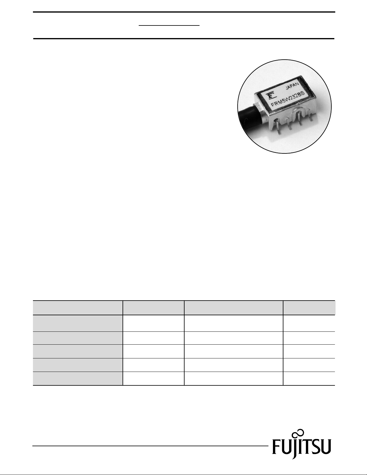
InGaAs-APD/Preamp
Receiver
FRM5W232BS/BS-A
Parameter Symbol
Storage Temperature
T
stg
-40 to +85 °C
Operating Case Temperature
-40 to +85 °C
T
op
Supply Voltage
0 to +4.5 V
V
DD
APD Reverse Voltage
0 to VB (Note)
V
V
R
APD Reverse Current
3.0 mA
I
R(peak)
Ratings Unit
ABSOLUTE MAXIMUM RATINGS (Tc=25°C, unless otherwise specified)
Note: Since the VB may vary from device to device, VB data is attached to each device for reference.
.
FEATURES
• 2.7Gb/s APD Receiver module in an industry
standard mini-DIL package is available in gull-wing
or through-hole configuration
• High Sensitivity: -34 dBm (typ.)
• Differential Electrical Output
• Integral Thermistor and GaAs IC Preamp
• Wide operating temperature range: -40 to +85°C
APPLICATIONS
This APD detector preamp is intended to function as an
optical receiver in long haul SONET, SDH, and DWDM systems
operating up to 2.7Gb/s. The device operates in both the 1,310 and
1,550nm wavelength windows. The nominal 10KΩ integral thermistor allows
accurate monitoring of the APD temperature and facilitates the design of the
APD bias control circuits. The detector preamplifier has a differential electrical output.
DESCRIPTION
The FRM5W232BS incorporates a 30 micron InGaAs Avalanche Photodiode (APD)
detector, a GaAs IC transimpedance preamplifier, and a thermistor in a mini-DIL type
package. The APD is processed with modern MOVPE techniques resulting in reliable
performance over a wide range of operating conditions. The lens coupling system
and the single mode fiber are assembled using Nd: YAG welding techniques. The BS
package is designed for a surface mount PC board assembly, and the BS-A is designed
for through-hole mount assembly.
Page 2
2
InGaAs-APD/Preamp
Receiver
FRM5W232BS/BS-A
Parameter Symbol
OPTICAL & ELECTRICAL CHARACTERISTICS
(Tc=25°C, λ=1,550nm, VDD=+3.3V unless otherwise specified)
Limits
Power Supply Voltage
V
DD
Power Supply Current
I
DD
Maximum Output Voltage Swing
Optical Return Loss
APD Responsivity
R15
R13
R16
Minimum Sensitivity
P
r
Maximum Overload
P
max
V
clip
Bandwidth
BW
AC Transimpedance
Z
t
Temperature Coefficient of VB
γ
Peaking
dpk
Group Delay Deviation
GD
Output Return Loss
S22
APD Breakdown Voltage
VB
Lower Cut-Off Frequency
fcl
Equivalent Input Noise
Current Density
in
Test Conditions
λ = 1,550nm, M=1
λ = 1,610nm, M=1
λ = 1,310nm, M=1
2.488Gb/s, NRZ, PRBS=223-1,
BER=10
-10
, M=3
M=3, Note (3)
Note (4)
Saturated Output Voltage
Pin=-30dBm, M=10,
-3dB from 1MHz
Pin=-30dBm, f=100MHz,
Single-end
Note (1)
Pin=-30dBm, M=10,
from 1MHz
Pin=-30dBm, M=10,
from 500MHz to 1.75GHz
up to 1.75GHz
up to 2.5GHz
ID=10µA
Average within 2.2GHz
Unit
V
mA
A/W
dBm
Ta=25°C, Rext=14dB
Ta=-40°C ~ 85°C,
Rext=14dB
Ta=25°C, Rext=10dB
dBm
mV
ORL
-
-
-
-
Tc=25°C
dB
GHz
Ω
V/°C
dB
psec
dB
V
kHz
pA Hz
Note: (1) γ=∆VB/∆Tc
Note: (2) All the parameters are measured with 50Ω AC-coupled.
Note: (3) Defined by 10% distortion of wave form.
Note: (4) Test condition is 2.488Gb/s, NRZ, PRBS=2
23
-1, B.E.R.=10
-10
, VR=Optimum with fc=1866MHz Bessel.
kΩ
Thermistor Resistance
Rth
K
Typ.
3.30
45
0.85
0.70
0.80
-
-
-34.0
550
2.4
2200
0.12
-
100
-
-
50
50
9.5
-33.0
-33.0
-
10.0
3900
Thermistor B Constant
B
Max.
3.45
70
-
-
-
-
-33.0
800
-
2600
0.15
+2
-
-
-
65
75
11
-
-31.0
-
-
10.5
4000
Min.
3.15
-
0.80
-
0.75
-5
-
450
2.2
1800
0.08
-
-
10
5
40
-
-
-7
-
-
30
9.5
3800
Page 3

3
InGaAs-APD/Preamp
Receiver
FRM5W232BS/BS-A
Notes
Page 4

4
InGaAs-APD/Preamp
Receiver
FRM5W232BS/BS-A
Fujitsu Compound Semiconductor Products contain gallium arsenide
(GaAs) which can be hazardous to the human body and the environment.
For safety, observe the following procedures:
CAUTION
• Do not put this product into the mouth.
• Do not alter the form of this product into a gas, powder, or liquid
through burning, crushing, or chemical processing as these by-products
are dangerous to the human body if inhaled, ingested, or swallowed.
• Observe government laws and company regulations when discarding this
product. This product must be discarded in accordance with methods
specified by applicable hazardous waste procedures.
“BS” PACKAGE
(GULL-WING)
UNIT: mm
For further information please contact:
FUJITSU COMPOUND SEMICONDUCTOR, INC.
2355 Zanker Rd.
San Jose, CA 95131-1138, U.S.A.
Phone: (408) 232-9500
FAX: (408) 428-9111
www.fcsi.fujitsu.com
FUJITSU QUANTUM DEVICES EUROPE LTD.
Network House
Norreys Drive
Maidenhead, Berkshire SL6 4FJ
United Kingdom
TEL: +44 (0) 1628 504800
FAX: +44 (0) 1628 504888
FUJITSU QUANTUM DEVICES
SINGAPORE PTE LTD.
Hong Kong Branch
Rm. 1101, Ocean Centre, 5 Canton Rd. Tsim Sha Tsui,
Kowloon, Hong Kong
TEL: +852-23770226
FAX: +852-23763269
FUJITSU QUANTUM DEVICES LIMITED
Business Development Division
11th Floor, Hachioji Daiichi-Seimei Bldg.
3-20-6 Myojin-cho
Hachioji-city, Tokyo 192-0046, Japan
TEL: +81-426-43-5885
FAX: +81-426-43-5582
Fujitsu Limited reserves the right to change products and specifications without notice.
The information does not convey any license under rights of Fujitsu Limited or others.
© 2003 FUJITSU COMPOUND SEMICONDUCTOR, INC.
Printed in U.S.A. FCSI1103M200
“BS-A” PACKAGE
(THROUGH-HOLE)
UNIT: mm
7.62±0.2
(P2.54x3)
0.3±0.05
Pin Description
1. VR
2. GROUND
3. OUT +
4. GROUND
5. THERMISTOR
6. OUT -
7. GROUND
8. VDD
1000 min.
See Lead Detail
7.37±0.15
9.77±0.15
∅0.9±0.1
∅4.1±0.2
24.1±2.0
11.37±0.15
0.4±0.05
(0.5)
(2.0)
5.2MAX.
Detail of Lead
(R0.7)
0~10°
(0.5)
1.2±0.07
0.50±0.15
(#1)
(#4) (#5)
Top View
∅0.9±0.1
∅4.1±0.2
1000 min.
(#8)
4.5 MON.
7.37±0.15
7.87±0.15
24.1±2.0
0.4±0.05
11.37±0.15
(0.5)
(2.0)
5.2MAX.
(#1)
(#4) (#5)
7.62±0.2
(P2.54x3)
Pin Description
1. VR
2. GROUND
3. OUT +
4. GROUND
5. THERMISTOR
6. OUT -
7. GROUND
8. VDD
(#8)
Top View
 Loading...