

Page 1

FUJITSU MICROELECTRONICS
CONTROLLER MANUAL
PROGRAMMING MANUAL
CM71-00105-1E
FR81 Family
32-BIT MICROCONTROLLER
Page 2

Page 3

FR81 Family
32-BIT MICROCONTROLLER
PROGRAMMING MANUAL
For the information for microcontroller supports, see the following web site.
http://edevice.fujitsu.com/micom/en-support/
FUJITSU MICROELECTRONICS LIMITED
Page 4

Page 5

PREFACE
■ Objectives and targeted reader
FR81 Family is a 32 bit single chip microcontroller with CPU of new RISC Architecture as the core. FR81
Family has specifications that are optimum for embedded use requiring high performance CPU processing
power.
This manual explains the programming model and execution instructions for engineers developing a
product using this FR81 Family Microcontroller, especially the programmers who produce program s using
assembly language of the assembler for FR/FR80/FR81 Family.
For the rules of assembly grammar language and the method of use of Assembler Programs, kindly refer to
"FR Family Assembler Manual".
*: FR, the abbreviation of Fujitsu RISC controller, is a line of products of Fujitsu Microel ectroni cs Limited.
Other company names and brand names are the trademarks or registered trademarks of their respective
owners.
■ Organization of this Manual
This manual consists of the following 7 chapters and 1 supplement.
CHAPTER 1 OVERVIEW OF FR81 FAMILY CPU
This chapter describes the features of FR81 Family CPU and its differences from hitherto FR Family.
CHAPTER 2 MEMORY ARCHITECTURE
This chapter describes Memory Architecture of the CPU of FR81 Family. Memory Architecture is the
method of allocation of memory space and access to this memory space.
CHAPTER 3 PROGRAMMING MODEL
This chapter describes registers in the CPU existing as programming model of FR81 Family CPU.
CHAPTER 4 RESET AND "EIT" PROCESSING
This chapter describes resetting of FR81 Family CPU and EIT processing. EIT processing is the generic
term for exceptions, interruption and trap.
CHAPTER 5 PIPELINE OPERATION
This chapter describes pipeline operation and delay divergence, the salient feature of FR81 Family CPU.
CHAPTER 6 INSTRUCTION OVERVIEW
This chapter describes outline of commands of FR81 Family CPU.
CHAPTER 7 DETAILED EXECUTION INSTRUCTIONS
This chapter describes Execution Instructions of FR81 Family CPU in Reference Format in the
alphabetical order.
APPENDIX
It contains instruction list and instruction map of FR81 Family CPU.
i
Page 6

• The contents of this document are subject to change without notice.
Customers are advised to consult with sales representatives before ordering.
• The information, such as descriptions of function and application circuit examples, in this document are presented solely for the
purpose of reference to show examples of operations and uses of FUJITSU MICROELECTRONICS device; FUJITSU
MICROELECTRONICS does not warrant proper operation of the device with respect to use based on such information. When
you develop equipment incorporating the device based on such information, you must assume any responsibility arising out of
such use of the information. FUJITSU MICROELECTRONICS assumes no liability for any damages whatsoever arising out of
the use of the information.
• Any information in this document, including descriptions of function and schematic diagrams, shall not be construed as license
of the use or exercise of any intellectual property right, such as patent right or copyright, or any other right of FUJITSU
MICROELECTRONICS or any third party or does FUJITSU MICROELECTRONICS warrant non-infringement of any thirdparty's intellectual property right or other right by using such information. FUJITSU MICROELECTRONICS assumes no
liability for any infringement of the intellectual property rights or other rights of third parties which would result from the use of
information contained herein.
• The products described in this document are designed, developed and manufactured as contemplated for general use, including
without limitation, ordinary industrial use, general office use, personal use, and household use, but are not designed, developed
and manufactured as contemplated (1) for use accompanying fatal risks or dangers that, unless extremely high safety is secured,
could have a serious effect to the public, and could lead directly to death, personal injury, severe physical damage or other loss
(i.e., nuclear reaction control in nuclear facility, aircraft flight control, air traffic control, mass transport control, medical life
support system, missile launch control in weapon system), or (2) for use requiring extremely high reliability (i.e., submersible
repeater and artificial satellite).
Please note that FUJITSU MICROELECTRONICS will not be liable against you and/or any third party for any claims or
damages arising in connection with above-mentioned uses of the products.
• Any semiconductor devices have an inherent chance of failure. You must protect against injury, damage or loss from such
failures by incorporating safety design measures into your facility and equipment such as redundancy, fire protection, and
prevention of over-current levels and other abnormal operating conditions.
• Exportation/release of any products described in this document may require necessary procedures in accordance with the
regulations of the Foreign Exchange and Foreign Trade Control Law of Japan and/or US export control laws.
• The company names and brand names herein are the trademarks or registered trademarks of their respective owners.
Copyright ©2009 FUJITSU MICROELECTRONICS LIMITED All rights reserved.
ii
Page 7

CONTENTS
CHAPTER 1 OVERVIEW OF FR81 FAMILY CPU ............................................................ 1
1.1 Features of FR81 Family CPU ............................................................................................................ 2
1.2 Changes from the earlier FR Family ................................................................................................... 4
CHAPTER 2 MEMORY ARCHITECTURE ........................................................................ 7
2.1 Address Space ................................................................................................................................... 8
2.1.1 Direct Address Area ..................................................................................................................... 8
2.1.2 Vector Table Area .......................................................................................................................... 9
2.1.3 20-bit Addressing Area & 32-bit Addressing Area ....................................................................... 11
2.2 Data Structure ................................................................................................................................... 12
2.2.1 Byte Data .............. ... ... .... ...................................... .... ... ... ....................................... . ..................... 12
2.2.2 Half Word Data ............................................... ... ... .... ... ....................................... ... ... .. ................. 12
2.2.3 Word Data ................................................................................................................................... 12
2.2.4 Byte Order .................. .... ... ... ....................................... ... ... .... ...................................................... 13
2.3 Word Alignment ................................................................................................................................ 14
2.3.1 Program Access ......................................................................................................................... 14
2.3.2 Data Access ............................................................................................................................... 14
CHAPTER 3 PROGRAMMING MODEL .......................................................................... 15
3.1 Register Configuration ...................................................................................................................... 16
3.2 General-purpose Registers ............................................................................................................... 17
3.2.1 Configuration of General-purpose Registers ............................................................................... 17
3.2.2 Special Usage of General-purpose Registers ............................................................................ 18
3.2.3 Relation between Stack Pointer and R15 .................................................................................... 18
3.3 Dedicated Registers ......................................................................................................................... 19
3.3.1 Configuration of Dedicated Registers .......................................................................................... 19
3.3.2 Program Counter (PC) ................................................................................................................. 20
3.3.3 Program Status (PS) ................................................................................................................... 20
3.3.4 System Status Register (SSR) .................................................................................................... 21
3.3.5 Interrupt Level Mask Register (ILM) ............................................................................................ 22
3.3.6 Condition Code Register (CCR) .................................................................................................. 23
3.3.7 System Condition Code Register (SCR) .................................................................................... 25
3.3.8 Return Pointer (RP) ..................................................................................................................... 26
3.3.9 System Stack Pointer (SSP) ....................................................................................................... 27
3.3.10 User Stack Pointer (USP) ............................................................................................................ 28
3.3.11 Table Base Register (TBR) ......................................................................................................... 29
3.3.12 Multiplication/Division Register (MDH, MDL) ............................................................................... 30
3.3.13 Base Pointer (BP) ........................................................................................................................ 32
3.3.14 FPU Control Register (FCR) ................................. ....................................... ... .... ... ...................... 32
3.3.15 Exception status register (ESR) .................................................................................................. 37
3.3.16 Debug Register (DBR) ................................................................................................................. 39
3.4 Floating-point Register ...................................................................................................................... 40
iii
Page 8

CHAPTER 4 RESET AND "EIT" PROCESSING ............................................................ 41
4.1 Reset ................................................................................................................................................ 42
4.2 Basic Operations in EIT Processing ................................................................................................. 43
4.2.1 Types of EIT Processing and Prior Preparation .......................................................................... 43
4.2.2 EIT Processing Sequence ........................................ ... ... ....................................... ... ... ... ............. 44
4.2.3 Recovery from EIT Processing .................................................................................................... 45
4.3 Processor Operation Status .............................................................................................................. 46
4.4 Exception Processing .......................... ....................................... ... ... ... ............................................. 48
4.4.1 Invalid Instruction Exception ........................................................................................................ 48
4.4.2 Instruction Access Protection Violation Exception ....................................................................... 49
4.4.3 Data Access Protection Violation Exception ................................................................................ 49
4.4.4 FPU Exception ... ... ... ... .... ...................................... .... ... ... ....................................... ... ................... 50
4.4.5 Instruction Break .......................................................................................................................... 51
4.4.6 Guarded Access Break ................................ ... ... ... .... ...................................... .... ... ... ................... 52
4.5 Interrupts .......................... ............. .......... ............. ............. ............. ............. ............ .......................... 53
4.5.1 General interrupts ........................................................................................................................ 53
4.5.2 Non-maskable Interrupts (NMI) ................................................................................................... 55
4.5.3 Break Interrupt ...... ... ... ....................................... ... .... ... ....................................... ... ...................... 55
4.5.4 Data Access Error Interrupt ......................................................................................................... 56
4.6 Traps ............................. .......... .......... ......... ....... ......... .......... .......... ......... .......... ................................ 57
4.6.1 INT Instructions ....................................... .... ... ... ....................................... ... ... .... ......................... 57
4.6.2 INTE Instruction ........................................................................................................................... 57
4.6.3 Step Trace Traps ........................................................................................................................ 58
4.7 Multiple EIT processing and Priority Levels ...................................................................................... 60
4.7.1 Multiple EIT Processing ............................................................................................................... 60
4.7.2 Priority Levels of EIT Requests ......... ... ....................................... ... ... .... ...................................... 61
4.7.3 EIT Acceptance when Branching Instruction is Executed ........................................................... 62
4.8 Timing When Register Settings Are Reflected ................................................................................. 63
4.8.1 Timing when the interrupt enable flag (I) is requested ................................................................ 63
4.8.2 Timing of Reflection of Interrupt Level Mask Register (ILM) ....................................................... 64
4.9 Usage Sequence of General Interrupts ............................................................................................ 65
4.9.1 Preparation while using general interrupts .................................................................................. 65
4.9.2 Processing during an Interrupt Processing Routine .................................................................... 66
4.9.3 Points of Caution while using General Interrupts ........................................................................ 66
4.10 Precautions .......................... .......................................... .......................................... ......................... 67
4.10.1 Exceptions in EIT Sequence and RETI Sequence ...................................................................... 67
4.10.2 Exceptions in Multiple Load and Multiple Store Instructions ....................................................... 67
4.10.3 Exceptions in Direct Address Transfer Instruction ....................................................................... 67
CHAPTER 5 PIPELINE OPERATION ............................................................................. 69
5.1 Instruction execution based on Pipeline ........................................................................................... 70
5.1.1 Integer Pipeline ............................................................................................................................ 70
5.1.2 Floating Point Pipeline ................................................................................................................. 72
5.2 Pipeline Operation and Interrupt Processin g .................................... ... ... .... ... ................................... 73
5.2.1 Mismatch in Acceptance and Cancellation of Interrupt ............................................................... 73
5.2.2 Method of preventing the mismatched pipeline conditions .......................................................... 73
5.3 Pipeline hazards ............................... ...................................... .... ... ... ................................................ 74
iv
Page 9

5.3.1 Occurrence of data hazard .......................................................................................................... 74
5.3.2 Register Bypassing ............................... ... .... ... ... ... ....................................... ... .... ... ... ................... 74
5.3.3 Interlocking .................................................................................................................................. 75
5.3.4 Interlocking produced by reference to R15 after Changing the Stack flag (S) ............................ 75
5.3.5 Structural Hazard ......................................................................................................................... 75
5.3.6 Control Hazard ............................................................................................................................ 76
5.4 Non-block loading ............................................................................................................................. 77
5.5 Delayed branching processing ......................................................................................................... 78
5.5.1 Example of branching with non-delayed branching instructions .................................................. 78
5.5.2 Example of processing of delayed branching instruction ............................................................ 79
CHAPTER 6 INSTRUCTION OVERVIEW ....................................................................... 81
6.1 Instruction System ............................ ...................................... .... ... ... ................................................ 82
6.1.1 Integer Type Instructions ............................................................................................................. 82
6.1.2 Floating Point Type Instructions .................................................................................................. 84
6.2 Instructions Formats ......................................................................................................................... 85
6.2.1 Instructions Notation Formats ...................................................................................................... 85
6.2.2 Addressing Formats .................................... ... ....................................... ... ... ... ............................. 86
6.2.3 Instruction Formats ...................................................................................................................... 87
6.2.4 Register designated Field .................................................................. .... ... ... ... .... ......................... 91
6.3 Data Format ...................................................................................................................................... 93
6.3.1 Data Format Used by Integer Type Instructions (Common with All FR Family) .......................... 93
6.3.2 Format Used for Floating Point Type Instructions ....................................................................... 94
6.4 Read-Modify-Write type Instructions ................................................................................................. 96
6.5 Branching Instructions and Delay Slot .............................................................................................. 97
6.5.1 Delayed Branching Instructions ................................................................................................... 97
6.5.2 Specific example of Delayed Branching Instructions ................................................................... 98
6.5.3 Non-Delayed Branching Instructions ........................................................................................... 99
6.6 Step Division Instructions ............................................................................................................... 100
6.6.1 Signed Division .......................................................................................................................... 100
6.6.2 Unsigned Division ...................................................................................................................... 101
CHAPTER 7 DETAILED EXECUTION INSTRUCTIONS .............................................. 103
7.1 ADD (Add 4bit Immediate Data to Destination Register) ................................................................ 105
7.2 ADD (Add Word Data of Source Register to Destination Register) ................................................ 107
7.3 ADD2 (Add 4bit Immediate Data to Destination Register) .............................................................. 109
7.4 ADDC (Add Word Data of Source Register and Carry Bit to Destination Register) ....................... 111
7.5 ADDN (Add Immediate Data to Destination Register) .................................................................... 113
7.6 ADDN (Add Word Data of Source Register to Destination Register) ............................................. 115
7.7 ADDN2 (Add Immediate Data to Destination Register) .................................................................. 117
7.8 ADDSP (Add Stack Pointer and Immediate Data) .......................................................................... 119
7.9 AND (And Word Data of Source Register to Data in Memory) ....................................................... 121
7.10 AND (And Word Data of Source Register to Destination Register) ................................................ 123
7.11 ANDB (And Byte Data of Source Register to Data in Memory) ...................................................... 125
7.12 ANDCCR (And Condition Code Register and Immediate Data) ..................................................... 127
7.13 ANDH (And Halfword Data of Source Register to Data in Memory) ............................................... 129
7.14 ASR (Arithmetic shift to the Right Direction) ..... ... ... ... .... ...................................... .... ... ... ................. 131
v
Page 10

7.15 ASR (Arithmetic shift to the Right Direction) ..... ... ... ... .... ...................................... .... ... ... ................. 133
7.16 ASR2 (Arithmetic shift to the Right Direction) ................................................................................. 135
7.17 BANDH (And 4bit Immediate Data to Higher 4bit of Byte Data in Memory) ................................... 137
7.18 BANDL (And 4bit Immediate Data to Lower 4bit of Byte Dat a in Me m or y) .......................... ........... 139
7.19 Bcc (Branch relative if Condition satisfied) ..................................................................................... 141
7.20 Bcc:D (Branch relative if Condition satisfied) .................................................................................. 143
7.21 BEORH (Eor 4bit Immediate Data to Higher 4bit of Byte Data in Memory) .................................... 145
7.22 BEORL (Eor 4bit Immediate Data to Lower 4bit of Byte Data in Me mor y) .... ... ... ........................... 147
7.23 BORH (Or 4bit Immediate Data to Higher 4bit of Byte Data in Memory) ........................................ 149
7.24 BORL (Or 4bit Immediate Data to Lower 4bit of Byte Dat a in Me m or y) ........................................ . 151
7.25 BTSTH (Test Higher 4bit of Byte Data in Memory) ......................................................................... 153
7.26 BTSTL (Test Lower 4bit of Byte Data in Memory) .......................................................................... 155
7.27 CALL (Call Subroutine) .............. ... .... ... ... ... ....................................... ... ... .... ... ................................. 157
7.28 CALL (Call Subroutine) .............. ... .... ... ... ... ....................................... ... ... .... ... ................................. 159
7.29 CALL:D (Call Subroutine) ............................................................................................................... 161
7.30 CALL:D (Call Subroutine) ............................................................................................................... 163
7.31 CMP (Compare Immediate Data and Destination Register) ........................................................... 165
7.32 CMP (Compare Word Data in Source Register and Destination Register) .................................... 167
7.33 CMP2 (Compare Immediate Data and Destination Register) ......................................................... 169
7.34 DIV0S (Initial Setting Up for Signed Division) ................................................................................. 171
7.35 DIV0U (Initial Setting Up for Unsigned Division) ............................................................................. 173
7.36 DIV1 (Main Process of Division) ..................................................................................................... 175
7.37 DIV2 (Correction When Remain is zero) ........................................................................................ 177
7.38 DIV3 (Correction When Remain is zero) ........................................................................................ 179
7.39 DIV4S (Correction Answer for Signed Division) ............................................................................. 181
7.40 DMOV (Move Word Data from Direct Address to Register) ........................................................... 183
7.41 DMOV (Move Word Data from Register to Direct Address) ........................................................... 185
7.42 DMOV (Move Word Data from Direct Address to Post Increment Register Indirect Address) ....... 187
7.43 DMOV (Move Word Data from Post Increment Register Indirect Address to Direct Address) ....... 189
7.44 DMOV (Move Word Data from Direct Address to Pre Decrement Register Indirect Address) ....... 191
7.45 DMOV (Move Word Data from Post Increment Register Indirect Address to Direct Address) ....... 193
7.46 DMOVB (Move Byte Data from Direct Address to Register) .......................................................... 195
7.47 DMOVB (Move Byte Data from Register to Direct Address) .......................................................... 197
7.48 DMOVB (Move Byte Data from Direct Address to Post Increment Register Indirect Address) ...... 199
7.49 DMOVB (Move Byte Data from Post Increment Register Indirect Address to Direct Address) ...... 201
7.50 DMOVH (Move Halfword Data from Direct Address to Register) ................................................... 203
7.51 DMOVH (Move Halfword Data from Register to Direct Address) ................................................... 205
7.52 DMOVH (Move Halfword Data from Direct Address to Post Increment Register Indirect Address)
......................................................................................................................................................... 207
7.53 DMOVH (Move Halfword Data from Post Increment Register Indirect Address to Direct Address)
......................................................................................................................................................... 209
7.54 ENTER (Enter Function) ................... ... ... ... ... .... ...................................... .... ... ... ... ........................... 211
7.55 EOR (Exclusive Or Word Data of Source Register to Data in Memory) ......................................... 213
7.56 EOR (Exclusive Or Word Data of Source Register to Destination Register) .................................. 215
7.57 EORB (Exclusive Or Byte Data of Source Register to Data in Mem or y) ........................................ 217
7.58 EORH (Exclusive Or Halfword Data of Source Register to Data in Me m or y) ................................. 219
7.59 EXTSB (Sign Extend from Byte Data to Word Data) ...................................................................... 221
7.60 EXTSH (Sign Extend from Byte Data to Word Data) ........ ... ... .... ... ...................................... .... ... ... . 223
vi
Page 11

7.61 EXTUB (Unsign Extend from Byte Data to Word Data) .................................................................. 225
7.62 EXTUH (Unsign Extend from Byte Data to Word Data) .................................................................. 227
7.63 FABSs (Single Precision Floating Point Absolute Value) ............................................................... 229
7.64 FADDs (Single Precision Floating Point Add) ... ... ... ....................................... ... ... .... ....................... 230
7.65 FBcc (Floating Point Conditional Branch) ....................................................................................... 232
7.66 FBcc:D (Floating Point Conditional Branch with Delay Slot) .......................................................... 234
7.67 FCMPs (Single Precision Floating Point Compare) ........................................................................ 236
7.68 FDIVs (Single Precision Floating Point Division) .................................... .... ... ................................. 238
7.69 FiTOs (Convert from Integer to Single Precision Floating Point) .................................................... 240
7.70 FLD (Single Precision Floating Point Data Load) ............. ....................................... ... ... ... .............. 242
7.71 FLD (Single Precision Floating Point Data Load) ............. ....................................... ... ... ... .............. 243
7.72 FLD (Single Precision Floating Point Data Load) ............. ....................................... ... ... ... .............. 244
7.73 FLD (Single Precision Floating Point Data Load) ............. ....................................... ... ... ... .............. 245
7.74 FLD (Single Precision Floating Point Data Load) ............. ....................................... ... ... ... .............. 246
7.75 FLD (Load Word Data in Memory to Floating Register) ................................................................. 247
7.76 FLDM (Single Precision Floating Point Data Load to Multip le Re gister) .... ... ................................. 248
7.77 FMADDs (Single Precision Floating Point Multiply and Add) ......................................................... 250
7.78 FMOVs (Single Precision Floating Point Move) ............................. ... ... ... ....................................... . 252
7.79 FMSUBs (Single Precision Floating Point Multiply and Subtract) ................................................... 253
7.80 FMULs (Single Precision Floating Point Multiply) ... ... ....................................... ... .... ... .................... 255
7.81 FNEGs (Single Precision Floating Point sign reverse) ................................................................... 257
7.82 FSQRTs (Single Precision Floating Point Square Root) ................................................................ 258
7.83 FST (Single Precision Floating Point Data Store) ... ... ....................................... ... .... ... .................... 259
7.84 FST (Single Precision Floating Point Data Store) ... ... ....................................... ... .... ... .................... 260
7.85 FST (Single Precision Floating Point Data Store) ... ... ....................................... ... .... ... .................... 261
7.86 FST (Single Precision Floating Point Data Store) ... ... ....................................... ... .... ... .................... 262
7.87 FST (Single Precision Floating Point Data Store) ... ... ....................................... ... .... ... .................... 263
7.88 FST (Store Word Data in Floating Point Register to Memory) ........................................................ 264
7.89 FSTM (Single Precision Floating Point Data Store from Multiple Register) .................................... 265
7.90 FsTOi (Convert from Single Precision Floating Point to Integer) .................................................... 267
7.91 FSUBs (Single Precision Floating Point Subtract) ................................................................... ... ... . 269
7.92 INT (Software Interrupt) .................................................... ... ... ....................................... . ................ 271
7.93 INTE (Software Interrupt for Emulator) ....................................... ... ... ... ... ........................................ 273
7.94 JMP (Jump) .................................................................................................................................... 275
7.95 JMP:D (Jump) ................................................................................................................................. 277
7.96 LCALL (Long Call Subroutine) ........................................................................................................ 279
7.97 LCALL:D (Long Call Subroutine) .................................................................................................... 280
7.98 LD (Load Word Data in Memory to Register) ................................... ... ... .... ... ................................. 281
7.99 LD (Load Word Data in Memory to Register) ................................... ... ... .... ... ................................. 283
7.100 LD (Load Word Data in Memory to Register) ...... ... ....................................... ... ... .... ....................... 285
7.101 LD (Load Word Data in Memory to Register) ...... ... ....................................... ... ... .... ....................... 287
7.102 LD (Load Word Data in Memory to Register) ...... ... ....................................... ... ... .... ....................... 289
7.103 LD (Load Word Data in Memory to Register) ...... ... ....................................... ... ... .... ....................... 291
7.104 LD (Load Word Data in Memory to Register) ...... ... ....................................... ... ... .... ....................... 292
7.105 LD (Load Word Data in Memory to Program Status Register) ................................................ ... ... . 294
7.106 LDI:20 (Load Immediate 20bit Data to Destination Register) ......................................................... 296
7.107 LDI:32 (Load Immediate 32 bit Data to Destination Register) ........................................................ 298
vii
Page 12

7.108 LDI:8 (Load Immediate 8bit Data to Destination Register) ............................................................. 300
7.109 LDM0 (Load Multiple Registers) ..................................................................................................... 302
7.110 LDM1 (Load Multiple Registers) ..................................................................................................... 304
7.111 LDUB (Load Byte Data in Memory to Register) .............................................................................. 306
7.112 LDUB (Load Byte Data in Memory to Register) .............................................................................. 308
7.113 LDUB (Load Byte Data in Memory to Register) .............................................................................. 310
7.114 LDUB (Load Byte Data in Memory to Register) .............................................................................. 312
7.115 LDUH (Load Halfword Data in Memory to Register) ....................................................................... 313
7.116 LDUH (Load Halfword Data in Memory to Register) ....................................................................... 315
7.117 LDUH (Load Halfword Data in Memory to Register) ....................................................................... 317
7.118 LDUH (Load Halfword Data in Memory to Register) ....................................................................... 319
7.119 LEAVE (Leave Function) ................................................................................................................ 320
7.120 LSL (Logical Shift to the Left Direction) ......................................... ... ... ........................................... 322
7.121 LSL (Logical Shift to the Left Direction) ......................................... ... ... ........................................... 324
7.122 LSL2 (Logical Shift to the Left Direction) ........................................................................................ 326
7.123 LSR (Logical Shift to the Right Direction) ....................................................................................... 328
7.124 LSR (Logical Shift to the Right Direction) ....................................................................................... 330
7.125 LSR2 (Logical Shift to the Right Direction) ..................................................................................... 332
7.126 MOV (Move Word Data in Source Register to Destination Register) ............................................. 334
7.127 MOV (Move Word Data in Source Register to Destination Register) ............................................. 336
7.128 MOV (Move Word Data in Program Status Register to Destination Register) ................................ 338
7.129 MOV (Move Word Data in Source Register to Destination Register) ............................................. 340
7.130 MOV (Move Word Data in Source Register to Program Status Register) ...................................... 342
7.131 MOV (Move Word Data in General Purpose Register to Floating Point Register) ......................... 344
7.132 MOV (Move Word Data in Floating Point Register to General Purpose Register) ......................... 345
7.133 MUL (Multiply Word Data) .............................................................................................................. 346
7.134 MULH (Multiply Halfword Data) ...................................................................................................... 348
7.135 MULU (Multiply Unsigned Word Data) ............................................................................................ 350
7.136 MULUH (Multiply Unsigned Halfword Data) . .... ... ... ... .... ...................................... .... ... ... ................. 352
7.137 NOP (No Operation) ....................................................................................................................... 354
7.138 OR (Or Word Data of Source Register to Data in Memory) ............................................................ 356
7.139 OR (Or Word Data of Source Register to Destination Register) ..................................................... 358
7.140 ORB (Or Byte Data of Source Register to Data in Memory) ........................................................... 360
7.141 ORCCR (Or Condition Code Register and Immediate Data) .. .... ...................................... ... .... ... .... 362
7.142 ORH (Or Halfword Data of Source Register to Data in Memory) ................................................... 364
7.143 RET (Return from Subroutine) ........................................................................................................ 366
7.144 RET:D (Return from Subroutine) .................................................................................................... 368
7.145 RETI (Return from Interrupt) ... ... ... ....................................... ... .... ... ................................... .............. 370
7.146 SRCH0 (Search First Zero bit position distance From MSB) .......................................................... 373
7.147 SRCH1 (Search First One bit position distance From MSB) ......................... ... ... ........................... 375
7.148 SRCHC (Search First bit value change position distance From MSB) ........................................... 377
7.149 ST (Store Word Data in Register to Memory) ................................................................................. 379
7.150 ST (Store Word Data in Register to Memory) ................................................................................. 381
7.151 ST (Store Word Data in Register to Memory) ................................................................................. 383
7.152 ST (Store Word Data in Register to Memory) ................................................................................. 385
7.153 ST (Store Word Data in Register to Memory) ................................................................................. 387
7.154 ST (Store Word Data in Register to Memory) ................................................................................. 389
viii
Page 13

7.155 ST (Store Word Data in Register to Memory) ................................................................................. 390
7.156 ST (Store Word Data in Program Status Register to Memory) ....................................................... 392
7.157 STB (Store Byte Data in Register to Memory) ................................................................................ 394
7.158 STB (Store Byte Data in Register to Memory) ................................................................................ 396
7.159 STB (Store Byte Data in Register to Memory) ................................................................................ 398
7.160 STB (Store Byte Data in Register to Memory) ................................................................................ 400
7.161 STH (Store Halfword Data in Register to Memory) ......................................................................... 401
7.162 STH (Store Halfword Data in Register to Memory) ......................................................................... 403
7.163 STH (Store Halfword Data in Register to Memory) ......................................................................... 405
7.164 STH (Store Halfword Data in Register to Memory) ......................................................................... 407
7.165 STILM (Set Immediate Data to Interrupt Level Mask Register) ...................................................... 408
7.166 STM0 (Store Multiple Registers) ..................................................................................................... 410
7.167 STM1 (Store Multiple Registers) ..................................................................................................... 412
7.168 SUB (Subtract Word Data in Source Register from Destination Register) ..................................... 414
7.169 SUBC (Subtract Word Data in Source Register and Carry bit from Destination Register) ............. 416
7.170 SUBN (Subtract Word Data in Source Register from Destination Register) ................................... 418
7.171 XCHB (Exchange Byte Data) .......................................................................................................... 420
APPENDIX ......................................................................................................................... 423
APPENDIX A Instruction Lists ............................................................................................................ 424
A.1 Meaning of Symbols .. ... ... .... ...................................... .... ... ... ....................................... ... ................. 425
A.1.1 Mnemonic and Operation Columns ...................................... ... ... ... ....................................... . 425
A.1.2 Operation Column ................................................................................................................. 430
A.1.3 Format Column ...................................................................................................................... 431
A.1.4 OP Column ............................................................................................................................ 431
A.1.5 CYC Column .......................................................................................................................... 432
A.1.6 FLAG Column ........................................................................................................................ 433
A.1.7 RMW Column ............................. ... ... ....................................... ... ... .... .................................... 433
A.1.8 Reference Column ................................................................................................................. 433
A.2 Instruction Lists .............................................................................................................................. 434
A.3 List of Instructions that can be positioned in the Delay Slot ........................................................... 448
APPENDIX B Instruction Maps ........................................................................................................... 450
B.1 Instruction Maps ............................................................................................................................. 451
B.2 Extension Instruction Maps ............................................................................................................ 452
APPENDIX C Supplemental Explanation about FPU Exception Processing ...................................... 455
C.1 Conformity with IEEE754-1985 Standard ...................................................................................... 455
C.2 FPU Exceptions ............................................................................................................................. 456
C.3 Round Processing .. ... ... ....................................... ... ... .... ...................................... .... ... ... ................. 458
INDEX...................................................................................................................................461
ix
Page 14

x CM71-00105-1E FUJITSU MICROELECTRONICS LIMITED 1
Page 15

CHAPTER 1
OVERVIEW OF FR81 FAMILY
CPU
This chapter describes the features of FR81 Family CPU
and the changes from the earlier FR Family.
1.1 Features of FR81 Family CPU
1.2 Changes from the earlier FR Family
Page 16

CHAPTER 1 OVERVIEW OF FR81 FAMILY CPU
1.1
FR81 Family
1.1 Features of FR81 Family CPU
FR81 Family CPU is meant for 32 bit RISC controller having proprietary FR81
architecture of Fujitsu. The FR81 architecture is optimized for microcontrollers by using
the FR family instruction set and including improved floating-point, memory protection,
and debug functions.
■ General-purpose Register Architecture
It is load/store architecture based on 16 numbers of 32-bit General-purpose registers R0 to R15. The
architecture also has instructions that are suitable for embedded uses such as memory to memory transfer,
bit processing etc.
■ Linear Space for 32-bit (4G bytes) addressing
Address space is controlled for each byte unit. Linear specification of Address is made based on 32-bit
address.
■ 16-bit fixed instruction length (excluding immediate data transfer instructions)
It is 16-bit fixed length instruction format excluding 32/20-bit immediate data transfer instruction. It
enables securing high object efficiency.
■ Floating point calculation unit (FPU)
FR81 Family supports single precision floating point calculation (IEEE754 compliant). It has 16 pieces of
32-bit floating point registers from FR0 to FR15. A single instruction can execute a product-sum operation
type calculation (multiplication, or addition/subtraction). The instruction length of a floating point type
instruction is 32 bits
■ Pipeline Configuration
High speed one-instruction one-cycle processing of the basic instructions based on 5-stage pipeline
operation can be carried out. Pipeline has following 5-stage configuration.
• IF Stage: Load Instruction
• ID Stage: Interpret Instruction
• EX Stage: Execute Instruction
• MA Stage: Memory Access
• WB Stage: Write to register
FR81 Family has the 6-stage pipeline configuration to execute floating point type instructions.
■ Non-blocking load
In FR81 Family, non-blocking loading is carried out m aking execution of LD (load) instructions efficient.
A maximum of four LD (Load) instructions can be issued in anticipation. In non-blocking, succeeding
instruction is executed without waiting for the completion o f a load instruction, in case general-purpose
register storing the value of load instruction is not referred by the succeeding instruction.
2 FUJITSU MICROELECTRONICS LIMITED CM71-00105-1E
Page 17

CHAPTER 1 OVERVIEW OF FR81 FAMILY CPU
FR81 Family
■ Harvard Architecture
An instruction can be executed efficiently based on Harvard Architecture where instruction bus for
instruction access and data bus for data access are independent.
■ Multiplication Instruction
Multiplication/division computation can be executed at the instructio n level based on an in-built mult iplier.
32-bit multiplication, signed or unsigned, is executed in 5 cycles. 16-bit multiplication is executed in 3
cycles.
■ Step Division Instruction
32-bit ÷ 32-bit division, signed or unsigned, can be executed based on combination of step division
instructions.
■ Direct Addressing Instruction for peripheral access
Address of 256 words/ 256 half-words/ 256 bytes from the top of address space (low order address) can be
directly specified. It is convenient for address specification in the I/O Register of the peripheral resource.
1.1
■ High-speed interrupt processing complete within 6 cycles
Acceptance of interruption is processed at a high speed within 6 cycles. A 16-level priority order is given to
the request for interruption. Masking in line with the priority order can be carried out based on interruption
mask level of the CPU.
CM71-00105-1E FUJITSU MICROELECTRONICS LIMITED 3
Page 18

CHAPTER 1 OVERVIEW OF FR81 FAMILY CPU
1.2
FR81 Family
1.2 Changes from the earlier FR Family
FR81 Family has partial addition and deletion of instructions and operational changes
from the earlier FR Family (FR30 Family, FR60 Family etc.).
■ Instructions that cannot be used in FR81/FR80 Family
Following instructions cannot be used in FR81/FR80 Family.
• Coprocessor Instructions (COPOP, COPLD, COPST, COPSV)
• Resource Instructions (LDRES, STRES)
Undefined Instruction Exceptions and not the Coprocessor Error Trap occur when execution of
Coprocessor Instruction is attempted. Undefined In struction Exceptions occur when execution of Resource
Instruction is attempted.
■ Instructions added to FR81/FR80 Family
Following instructions have been added in FR81/FR80 Family. These instructions have replaced the bit
search module embedded as a peripheral function.
• SRCH1 (Bit Search Instruction Detection of First "1" bit from MSB to LSB)
• SRCH0 (Bit Search Instruction Detection of first "0" bit from MSB to LSB)
• SRCHC (Bit Search Instruction Detection of Change point from MSB to LSB)
see "Chapter 7 Detailed Execution Instructions" and "Appendix A 2 Instruction Lists" for operation of Bit
Search Instructions.
■ Adding floating point type instructions
Floating point type instructions and 16 pieces of 32-bit floating point registers (FR0 to FR15) have been
added in FR81 Family.
■ Privilege mode
Privilege mode has been added in FR81 family. Privilege mode and user mode are two CPU operation
modes.
■ Exception processing
Exception processing has been improved for FR81 Family. The following exceptions have been added.
• FPU exception
• Instruction access protection violation exception
• Data access protection violation exception
• Invalid instruction exception (Changing definition from undefined instruction exception)
• Data access error exception
• FPU absence exception
4 FUJITSU MICROELECTRONICS LIMITED CM71-00105-1E
Page 19

CHAPTER 1 OVERVIEW OF FR81 FAMILY CPU
FR81 Family
■ Operation of INTE Instructions during Step Execution
In FR81 Family, trap processing is initiate d based on INTE instructions even during step execution based
on step trace trap.
In hitherto FR Family, trap processing is not initiated based on INTE inst ruct ions during step execution.
For trap processing based on step trace trap and INTE instructions, see “4.6 Traps”.
1.2
CM71-00105-1E FUJITSU MICROELECTRONICS LIMITED 5
Page 20

CHAPTER 1 OVERVIEW OF FR81 FAMILY CPU
1.2
FR81 Family
6 FUJITSU MICROELECTRONICS LIMITED CM71-00105-1E
Page 21

CHAPTER 2
MEMORY ARCHITECTURE
This chapter explains the memory architecture of FR81
Family CPU. Memory architecture refers to allocation of
memory spaces and methods used to access memory.
2.1 Address Space
2.2 Data Structure
2.3 Word Alignment
CM71-00105-1E FUJITSU MICROELECTRONICS LIMITED 7
Page 22
CHAPTER 2 MEMORY ARCHITECTURE
2.1
2.1 Address Space
The address space of FR81 Family CPU is 32 bits (4Gb yte).
CPU controls the address spaces in byte units. An address on the address space is accessed from the CPU
by specifying a 32-bit value. Address space is indicated in Figure 2.1-1.
Figure 2.1-1 Address space
FR81 Family
Direct address area
General addressing
0000 0000 H
0000 0100 H
0000 0200 H
0000 0400 H
000F FC00H
0010 0000H
FFFF FFFFH
Byte data
Half-word data
Word data
Vector table
initial area
Program or data area
Address space is also called memory space. It is a logical address space as seen from the CPU. Addresses
cannot be changed. Logical address as seen from the CPU, and the physical address actually allocated to
memory or I/O are identical.
2.1.1 Direct Address Area
In the lower address in the address space, there is a direct address area.
Direct address area directly specifies an address in the direct address specification instruction. This area
accesses only based on operand data in the instruction without the use of general-purpose registers. The
size of the address area that can be specified by direct addressing varies according to the data type being
accessed.
000F FC00
TBR initial value
H TBR
The correspondence between data type and area specified by direct address is as follows.
• byte data access: 0000 0000
• half-word data access: 0000 0000H to 0000 01FF
• word data access: 0000 0000H to 0000 03FF
to 0000 00FF
H
H
H
H
The method of using the 8-bit address data contained in the operand of instructions that specify direct
addresses is as follows:
8 FUJITSU MICROELECTRONICS LIMITED CM71-00105-1E
Page 23
FR81 Family
0000 0000H
FFFF FFFFH
TBR
1 Kbyte
Number
EIT source
FF
H
FEH
FDH
FCH
00H
000H
004H
008H
00CH
3FCH
Entry address for INT instruction
Entry address for INT instruction
Entry address for INT instruction
Entry address for INT instruction
Entry address for reset processing
Memory space
Vect or
table
area
• byte data access: Lower 8 bits of the address are used as it is
• half word data access: Value is doubled and used as lower 9 bits of the address
• word data access: Value is quadrupled and used as lower 10 bits of the address
The relation between data types specified by direct address and memory address is shown in Figure 2.1-2.
CHAPTER 2 MEMORY ARCHITECTURE
2.1
Figure 2.1-2
[Example 1] Byte data: DMOVB R13,@58H
[Example 2] Half-word data: DMOVH R13,@58H
[Example 3] Word data: DMOV R13,@58H
Relation between data type specified by direct address and memory address
Memory space
58
Object code:1A58H
Object code:192C
R13 12345678
Right 2-bit shift
Object c ode:1816
No data shift
Right 1-bit shift
H 58HLeft 1-bit shift
H 58HLeft 2-bit shi
f
t
0000 0058HR13 12345678
0000 0058
0000 0058
H
78
Memory space
H
5678
Memory space
HR13 12345678
1345678
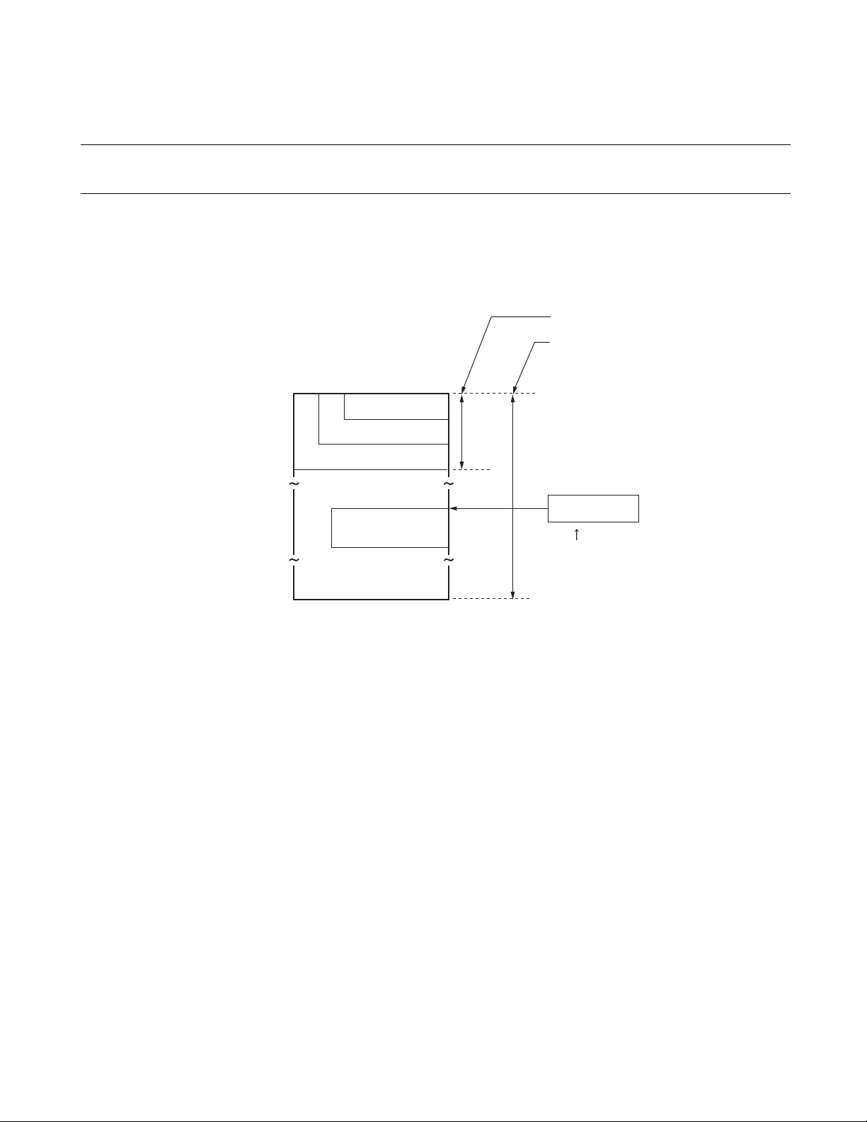
2.1.2 Vector Table Area
An area of 1Kbyte from the address shown in the Table Base Register (TBR) is called the EIT Vector Table
Area.
Table Base Register (TBR) represents the top address of the vector table area. In this vector table area, the
entry addresses of EIT processing (Exception processing, Interrupt processing, Trap processing) are
described. The relation between Table Base Register (TBR) and vector table area is shown in Figure 2.1-3.
Figure 2.1-3 Relation between Table Base Register (TBR) and Vector Table Area addresses
CM71-00105-1E FUJITSU MICROELECTRONICS LIMITED 9
Page 24

CHAPTER 2 MEMORY ARCHITECTURE
2.1
FR81 Family
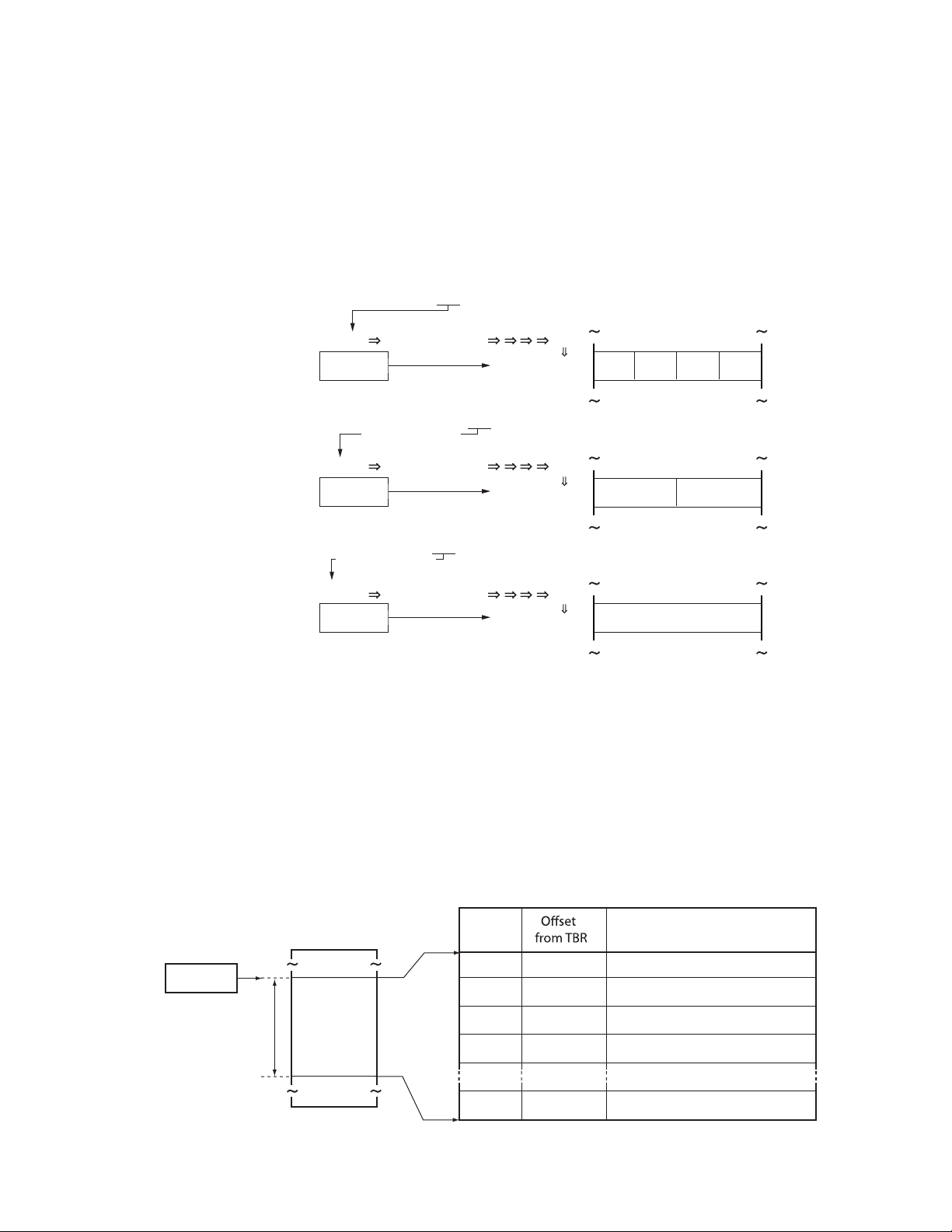
Table 2.1-1
Offset from
TBR
3FC
H
3F8
H
3F4
H
3F0
H
3EC
H
3E8
H
3E4
H
3E0
H
3DC
H
3D8
H
3D4
H
3D0
H
3CC
H
3C8
H
3C4
H
3C0
H
3BC
H
to
304
H
300
H
2FC
H
2F8
H
2F4
H
to
000
H
As a result of reset, the value of Table Base Register (TBR) is initialized to 000F FC00
vector table area extends from 000F FC00
to 000F FFFFH. By rewriting the Table Base Register (TBR),
H
, and the range of
H
the vector table area can be allocated to any desired location.
A vector table is composed of entry addresses for each EIT processing programs. Each vector table
contains values whose use is fixed according to the CPU architecture, and values that vary according to the
type of built-in peripheral functions. The structure of vector table area is shown in Table 2.1-1.
Structure of Vector Table Area
Vector
number
00
H
01
H
02
H
03
H
04
H
05
H
06
H
07
H
08
H
09
H
0A
H
0B
H
0C
H
0D
H
0E
H
0F
H
0F
H
to
3E
H
3F
H
40
H
41
H
42
H
to
FF
H
Model-
dependence
EIT value description Remarks
No reset
No system reserved
No system reserved Disabled
No system reserved Disabled
No system reserved Disabled
No FPU exception
No
No
Instruction access protection
violation exception
Data access protection
violation exception
No Data access error interrupt
No INTE instruction For use in the emulator
No Instruction break
No system reserved
No Step trace trap
No system reserved
No Invalid instruction exception
No NMI request
General interrupt
Yes
(used in external interrupt,
interrupt from peripheral
Refer to the Hardware Manual for each
model
function)
No General interrupts Used in Delayed interrupt
No system reserved Used in REALOS
No system reserved Used in REALOS
No Used in INT instruction
For vector tables of actual models, refer to the hardware manuals for each model.
10 FUJITSU MICROELECTRONICS LIMITED CM71-00105-1E
Page 25

CHAPTER 2 MEMORY ARCHITECTURE
FR81 Family
2.1.3 20-bit Addressing Area & 32-bit Addressing Area
The lower portion of the address space extending from 0000 0000H to 000F FFFFH (1Mbyte) will be the
20-bit addressing area. The overall address space from 0000 0000
addressing space.
If all the program locations and data locations are positioned within the 20-bit addressing area, a compact
and high-speed program can be realized as compared to a 32-bit addressing area.
In a 20-bit addressing area, as the address values are within 20 bits, the LDI:20 instruction can be used for
immediate loading of address information. The instruction length (Code size) of LDI:20 instruction is
4bytes. By using LDI:20 instruction, the program becomes more compact than when using LDI:32
instruction of instruction length 6bytes.
Example of 20-bit Addressing
Code size
LDI:20 #label20,Ri ; 4 bytes
JMP @Ri ; 2 bytes
to FFFF FFFFH will be 32-bit
H
2.1
Total 6 bytes
Example of 32-bit Addressing
Code size
LDI:32 #label32,Ri ; 6 bytes
JMP @Ri ; 2 bytes
Total 8 bytes
CM71-00105-1E FUJITSU MICROELECTRONICS LIMITED 11
Page 26

CHAPTER 2 MEMORY ARCHITECTURE
MSBbit76543210LSB
2.2
FR81 Family
2.2 Data Structure
FR81 Family CPU has three data types namely byte data (8-bits), half word data (16-bits)
and word data (32-bits). The byte order is big endian.
2.2.1 Byte Data
This is a data type having 8 bits as unit. Bit order is l ittle endian, MSB side becomes bit7 and LSB side
becomes bit0. The structure of byte data is shown in Figure 2.2-1.
Figure 2.2-1
2.2.2 Half Word Data
This is a data type having 16 bits (2byte) as unit . Bit order is little endian, MSB side is bit15 while LSB
side is bit0. Bit15 to bit8 of MSB side represent the higher bytes wh ile bit7 to bit0 of LSB side represent
the lower bytes. The structure of half word data is shown in Figure 2.2-2.
Figure 2.2-2
MSB
bit
Higher bytes Lower bytes
Structure of byte data
Structure of Half Word Data
LSB
789101112131415 6543210
2.2.3 Word Data
This is a data type having 32 bits (4byte) as unit . Bit order is little endian, MSB side is bit31 while LSB
side is bit0. Bit31 to bit16 of the MSB side become the higher half word, while bit1 5 to bit0 of the LSB
side become the lower half word. The structure of word data is shown in Figure 2.2-3.
Figure 2.2-3
MSB
bit31
Higher half word Lower half word
12 FUJITSU MICROELECTRONICS LIMITED CM71-00105-1E
Structure of Word Data
16 1524 23 8 7 0
LSB
Page 27

FR81 Family
2.2.4 Byte Order
The byte order of FR81 Family CPU is big endian. When word data or half word data are allocated to
address spaces, the higher bytes are placed in the lower address side while the lower bytes are placed in the
higher address side. The arrangement of big endian byte data is shown in Figure 2.2-4.
CHAPTER 2 MEMORY ARCHITECTURE
2.2
Byte
Half word
Word
For example, if a word data was written on the memory (RAM) at address location 0004 1234
memory space, the highest byte will be stored at location 0004 1234
at location byte 0004 1237
Address
MSB
Address Address +1
MSB
MSB
Higher byte Lower byte
Address Address +1 Address +2 Address +3
Highest byte Lowest byte
Higher half word Lower half word
.
H
Figure 2.2-4
LSB
Big Endian Byte Orde
LSB
while the lowest byte will be stored
H
H
LSB
of the
CM71-00105-1E FUJITSU MICROELECTRONICS LIMITED 13
Page 28

CHAPTER 2 MEMORY ARCHITECTURE
2.3
FR81 Family
2.3 Word Alignment
The data type used determines restrictions on the designation of memory addresses
(word alignment).
2.3.1 Program Access
Unit of instruction length is half word (2byte) and all instructions are allocated to addresses which are
multiples of 2 (2n location).
At the time of execution of the instruction, bit0 of the program counter (PC) automatically becomes "0",
and is always at an even address. In a branched instruction, even if an odd address is generated as a result
of branch destination address calculation, the bit0 of the address will be assigned "0" and branched to an
even address.
There is no address exception in program access.
2.3.2 Data Access
There are following restrictions on addresses for data access depending upon the data type used.
Word data
Data is assigned to addresses that are multiples of 4 (4n location). The restriction of multiples of 4
on addresses is called ‘word boundary’. If the specified address is not a multiple of 4, the lower two
bits of the address are set to "00" forcibly.
Half-word data
Data is assigned to addresses that are multiples of 2 (2n locations). The restr iction of multiples of 2
on addresses is called ‘half-word boundary’. If the specified address is not a multiple of 2, the lower
1 bit of the address is set to "0" forcibly.
Byte data
There is no restriction on allocation of addresses.
During word and half-word data access, condition that lower bit of an address has to be "0" is applicable
only for the result of computation of an effective address. Values still under calcula tion are used as they
are.
14 FUJITSU MICROELECTRONICS LIMITED CM71-00105-1E
Page 29

CHAPTER 3
PROGRAMMING MODEL
This chapter describes the programming model of FR81
Family CPU.
3.1 Register Configuration
3.2 General-purpose Registers
3.3 Dedicated Registers
3.4 Floating-point Register
CM71-00105-1E FUJITSU MICROELECTRONICS LIMITED 15
Page 30

CHAPTER 3 PROGRAMMING MODEL
3.1
FR81 Family
3.1 Register Configuration
FR81 Family CPU uses three types of registers, namely, general-purpose registers, dedicated
registers and floating point registers.
General-purpose registers are registers that store computation data and address information. They comprise
16 registers from R0 to R15. Dedicated registers are registers that store information for specific
applications.
Floating point registers are registers that store calculation inform ation for floating point calculations . They
are comprised of 16 registers from FR0 to FR15.
16 FUJITSU MICROELECTRONICS LIMITED CM71-00105-1E
Page 31

CHAPTER 3 PROGRAMMING MODEL
FR81 Family
3.2
3.2 General-purpose Registers
General-purpose registers are used for storing results of various calculations, as well
as information about addresses to be used as pointers for memory access.
3.2.1 Configuration of General-purpose Registers
General-purpose registers has sixteen each 32 bits in length. General-purpose registers have names R0 to
R15.
In case of general instructions, the general-purpose registers can use without any distinction. In some
instructions, three registers namely R13, R14 and R15 have special usages.
Figure 3.2-1 shows the configuration and initial values of general-purpose registers.
Figure 3.2-1 Configuration and initial values of general-purpose registers
32 bits
[Initial value]
R0
R1
R2
R3
R4
R5
R6
R7
R8
R9
R10
R11
R12
R13
R14
R15
R0 to R14 are not initialized as a result of reset. R15 is initialized 0000 0000
AC
FP
SP
as a result of reset.
H
CM71-00105-1E FUJITSU MICROELECTRONICS LIMITED 17
Page 32

CHAPTER 3 PROGRAMMING MODEL
3.2
3.2.2 Special Usage of General-purpose Registers
General-purpose registers R13 to R15, besides being used as other general-purpose registers, are used in the
following way in some instructions.
R13 (Virtual Accumulator: AC)
• Base address register for load/store to memory instructions
[Example: LD @(R13,Rj), Ri]
• Accumulator for direct address designation
[Example: DMOV @dir10, R13]
• Memory pointer for direct address designation
[Example: DMOV @dir10,@R13+]
R14 (Frame Pointer: FP)
• Index register for load/store to memory instructions
[Example: LD @(R14,disp10), Ri]
• Frame pointer for reserve/release of dynamic memory area
FR81 Family
[Example: ENTER #u10]
R15 (Stack Pointer: SP)
• Index register for load/store to memory instructions
[Example: LD @(R15,udisp6), Ri]
• Stack pointer
[Example: LD @R15+,Ri]
• Stack pointer for reserve/release of dynamic memory area
[Example: ENTER #u10]
3.2.3 Relation between Stack Pointer and R15
R15 functions as an indirect register. Physically it becomes either the system stack pointer (SSP) or user
pointer (USP) for dedicated registers. When the notation R15 is used in an instruction, this register will
function as USP if the stack flag (S) is "1" and as SSP if the stack flag is "0". Table 3.2-1 shows the
correlation between general-purpose register R15 and stack pointer.
When something is written on R15 as a general-purpose register, it is automatically written onto the system
stack pointer (SSP) or user stack pointer (USP) according to the value of stack flag (S).
Table 3.2-1 Correlation between General-purpose Register "R15" an d Stack Pointer
General-purpose register S Flag Stack pointer
R15
Stack flag (S) is present in the condition code register (CCR) section of the program status (PS).
18 FUJITSU MICROELECTRONICS LIMITED CM71-00105-1E
1 User stack pointer (USP)
0 System stack pointer (SSP)
Page 33

CHAPTER 3 PROGRAMMING MODEL
FR81 Family
3.3 Dedicated Registers
FR81 Family CPU has dedicated registers reserved for special usages.
3.3.1 Configuration of Dedicated Registers
Dedicated registers are used for special purposes. The following dedicated registers are available.
• Program counter (PC)
• Program status (PS)
• Return pointer (RP)
• System stack pointer (SSP)
• User stack pointer (USP)
• Table base register (TBR)
• Multiplication/Division Register (MDH, MDL)
• Base Pointer (BP)
3.3
• FPU control register (FCR)
• Exception status register (ESR)
• Debug register (DBR)
Figure 3.3-1 shows the configuration and initial values of dedicated registers.
Figure 3.3-1 Configuration and Initial Values of Dedicated Registers
32 bits
Program counter
Program status
Table base register
Return pointer
System stack pointer
User stack pointer
Multiplication/Division
registers
PC
PS
TBR
RP
SSP
USP
MDH
MDL
-
ILM
-
SCR CCR
[Initial value]
Base Pointer
FPU control register
Except status register
Debug register
BP
FCR
ESR
DBR
CM71-00105-1E FUJITSU MICROELECTRONICS LIMITED 19
Page 34

CHAPTER 3 PROGRAMMING MODEL
3.3
3.3.2 Program Counter (PC)
Program counter (PC) is a 32-bit register that indicates the address containing the instruction that is
currently executing.
Figure 3.3-2 shows the bit configuration of program counter (PC).
Figure 3.3-2 Program Counter (PC) Bit Configuration
FR81 Family
bit31
The value of the lowest bit (LBS) of the program counter (PC) is always read as “0”. Even if "1" is written
to it as a result of address calculation of branching destination, the lowest bit of branching address will be
treated as "0". When the program counter (PC) changes after the execution of an instruction and it indicates
the next instruction, the lowest bit is always read as "0".
Following a reset, the contents of the Program Counter (PC) are set to the value (reset entry address)
written in the reset vector of the vector table. As the table base register (TBR) is initialized first by reset,
the address of the reset vector will be 000F FFFC
3.3.3 Program Status (PS)
Program status (PS) is a 32-bit register that indicates the status of program execution. It sets the interrupt
enable level, controls the program trace break function in the CPU, and indicates the status of instruction
execution.
Program status (PS) consists of the following 4 parts.
• System status register (SSR)
bit0
Initial value
XXXX XXXX
.
H
H
• Interrupt level mask register (ILM)
• System condition code register (SCR)
• Condition code register (CCR)
Figure 3.3-3 shows the bit configuration of program status (PS).
Figure 3.3-3 Program status (PS) Bit Configuration
bit31 bit20bit27 bit15 bit10 bit7 bit0
Reserved Reserved
The reserved bits of program status (PS) are all reserved for future expansion. The read value of reserved
bits is always "0". Write values should always be written as "0".
20 FUJITSU MICROELECTRONICS LIMITED CM71-00105-1E
ILMSSR SCR CCR
Page 35

FR81 Family
MPUFPUUMDBG
bit31 bit30 bit29 bit28
Initial value
0011
B
3.3.4 System Status Register (SSR)
System status register (SSR) is a 4-bit register that indicates the state of the CPU. It lies between bit 31 and
bit 28 of the program status (PS).
Figure 3.3-4 shows the bit configuration of system status register (SSR).
Figure 3.3-4 System Status Register (SSR) Bit Configuration
The contents of each bit are described below.
[bit31] DBG: Debug State Flag
This flag indicates the debugging state during debugging. The flag bit is turned to "1" when the
system shifts to a debug state, and turned to "0" when moving from the debug state with a RETI
instruction. This cannot be rewritten using instructions such as the MOV instruction.
CHAPTER 3 PROGRAMMING MODEL
3.3
The initial value of the debug state flag (DBG) after a reset is "0".
[bit30] UM: User Mode Flag
This flag indicates the user mode. The flag bit is turned to "1" when the system is shifted to user
mode by the execution of a RETI instruction, and cleared to "0" when shifted to privilege mode with
EIT. Upon execution of the RETI instruction, if bit 30 of the PS value is set to "1", a value returned
from memory, the system shifts to user mode. This cannot be rewritten using instructions such as the
MOV instruction.
The initial value of the user mode flag (UM) after a reset is "0".
[bit29] FPU: FPU presence flag
This flag indicates that the floating point calculation unit (FPU) is installed. The flag bit is set to "1"
if a FPU is installed, and "0" if it is not the case. This bit cannot be rewritten.
Table 3.3-1 FPU presence flag (FPU) in the system status register
flag value Meaning
FPU
[bit28] MPU: MPU presence flag
This flag indicates that the memory protection unit (MPU) is installed. The flag bit is set to "1" if a
MPU is installed, and "0" if it is not the case. This bit cannot be rewritten.
Table 3.3-2 MPU presence flag (MPU) in the system status register
0 With FPU (installed)
1 Without FPU (not installed)
CM71-00105-1E FUJITSU MICROELECTRONICS LIMITED 21
flag value Meaning
MPU
0 With MPU (installed)
1 Without MPU (not installed)
Page 36

CHAPTER 3 PROGRAMMING MODEL
Interrupt controller
Interrupt activated
Peripheral
Interrupt
request
Activation OK
ICR
25
ILM
29
Comp
29>25
1
FR81 family CPU
AND
3.3
3.3.5 Interrupt Level Mask Register (ILM)
Interrupt level mask register (ILM) is a 5-bit register used to store the interrupt level mask value. It lies
between bit20 to bit16 of the program status (PS).
Figure 3.3-5 shows the bit configuration of interrupt level mask register (ILM).
Figure 3.3-5 Interrupt Level Mask Register (ILM) Bit Configuration
FR81 Family
bit20 bit19 bit18 bit17 bit16
ILM4 ILM3 ILM2 ILM1 ILM0
Initial value
01111
B
The value stored in interrupt level mask register (ILM), is used in the level mask of an interrupt. When the
interrupt enable flag (I) is "1", the value of interrupt level mask register (ILM) is compared to the level of
the currently requested interrupt. If the value of interrupt level mask register (ILM) is greater (i nter rupt
level is stronger), interrupt requested is accepted. Figure 3.3-6 shows the functions of interrupt level mask.
Figure 3.3-6 Functions of Interrupt Level Mask
The values of interrupt level range from 0(00000
the stronger it is, and the larger the value, the weaker it is. 0(00000
31(11111
) is the weakest.
B
) to 31(11111B). The smaller the value of interrupt level,
B
) is the strongest interrupt level, while
B
There are following restrictions on values of the interrupt level mask register (I LM) that can be set from a
program.
• When the value of interrupt level mask register (ILM) lies between 0(00000
from 0(00000
) to 31(11111B) can be set.
B
• When the value of interrupt level mask register (ILM) lies between 16(10000
values between 16(10000
• When setting of values between 0(00000
values between 16(10000
The interrupt level mask register (ILM) is initialized to 15(01111
) to 31(11111B) can be set.
B
) to 15(01111B) is attempted, 16 is added on automatically and
B
) to 31(11111B) are set.
B
) following a reset. If an interrupt request
B
) to 15(01111B), only values
B
) to 31(11111B), only
B
is accepted, the interrupt level corresponding to that interrupt is set in the interrupt level mask register
(ILM).
For setting a value in interrupt level mask register (ILM) from a program, the STILM instruction is used.
22 FUJITSU MICROELECTRONICS LIMITED CM71-00105-1E
Page 37

FR81 Family
3.3.6 Condition Code Register (CCR)
Condition code register (CCR) is an 8-bit register that indicates the status of instruction execution. It lies
between bit7 to bit0 of the program status (PS).
Figure 3.3-7 shows the bit configuration of condition code register (CC R ).
Figure 3.3-7 Condition Code Register (CCR) Bit Configuration
CHAPTER 3 PROGRAMMING MODEL
3.3
bit7 bit6 bit5 bit4 bit3bit2 bit1 bit0
CCR ReservedReserved
The contents of each bit are described below.
[bit7, bit6] Reserved
These are reserved bits. Read value is always "0". Write value should always be "0".
[bit5] S: Stack Flag
This flag selects the stack pointer to be used as general-purpose register R15. When the value of
stack flag (S) is "0", system stack pointer (SSP) is used, while when the value is "1", user stack
pointer (USP) is used.
Table 3.3-3 Stack Flag (S) of Condition Code Register
flag value Meaning
S
If an EIT operation is accepted, stack flag (S) automatically becomes "0". However, the value of the
condition code register (CCR) saved in system stack is the value which is later replaced by "0".
S INZVC
0 System stack pointer (SSP)
1 User stack pointer (USP)
Initial value
--00XXXX
B
The initial value of stack flag (S) after a reset is "0".
[bit4] I: Interrupt Enable Flag
This flag is used to enable/disable mask-able interrupts. The value "0" of interrupt enable flag (I)
disables an interrupt while "1" enables an interrupt. When an interrupt is enabled, the mask
operation of interrupt request is performed by interrupt level mask register (ILM).
Table 3.3-4 Interrupt Enable Flag (I) of Condition Code Register
flag Value Meaning
I
The value of this flag is replaced by "0" by execution of INT instruction. However, the value of
condition code register (CCR) saved in the system stack is the value which is later replaced by "0".
The initial value of an interrupt enable flag (I) after a reset is "0".
CM71-00105-1E FUJITSU MICROELECTRONICS LIMITED 23
0 Interrupt disable
1 Interrupt enable
Page 38

CHAPTER 3 PROGRAMMING MODEL
3.3
[bit3] N: Negative Flag
This flag is used to indicate positive or negative values when the results of a calculation are
expressed in two’s complement form. The value "0" of the negative flag (N) indicates a positive
value while "1" indicates a negative value.
Table 3.3-5 Negative Flag (N) of Condition Code Register
flag value Meaning
N
The initial value of Negative flag (N) after a reset is undefined.
[bit2] Z: Zero Flag
This flag indicates whether the result of a calculation is zero or not. The value "0" of zero flag (Z)
indicates a non-zero value, while "1" indicates a zero value.
Table 3.3-6 Zero Flag (Z) of Condition Code Register
flag value Meaning
Z
FR81 Family
0 Calculation result is a positive value
1 Calculation result is a negative value
0 Calculation result is a non-zero value
1 Calculation result is a zero value
The initial value of Zero flag (Z) after a reset is undefined.
[bit1] V: Overflow Flag
This flag indicates whether an overflow has occurred or not when the results of a calculation are
expressed in two’s complement form. The value "0" of an overflow flag (V) indicates no overflow,
while value "1" indicates an overflow.
Table 3.3-7 Overflow Flag (V) of Condition Code Register
flag value Meaning
V
Initial value of overflow flag (V) after a reset is indefinite
[bit0] C: Carry Flag
This flag indicates whether a carry or borrow condition has occurred in the highest bit of the results
of a calculation. The value "0" of the carry flag (C) indicates no carry or borrow, while a value "1"
indicates a carry or borrow condition.
Table 3.3-8 Carry Flag (C) of Condition Code Register
0 No overflow
1Overflow
flag value Meaning
C
The initial value of a carry flag (C) after reset is undefined.
24 FUJITSU MICROELECTRONICS LIMITED CM71-00105-1E
0 No carry or borrow
1 Carry or borrow condition
Page 39

CHAPTER 3 PROGRAMMING MODEL
FR81 Family
3.3.7 System Condition Code Register (SCR)
System condition code register (SCR) is a 3-bit register used to control the intermediate data of stepwise
division and step trace trap. It lies between bit10 to bit8 of the program status (PS).
Figure 3.3-8 shows the bit configuration of system condition code register (SCR).
Figure 3.3-8 System Condition Code Register (SCR) Bit Configuration
3.3
bit10 bit9 bit8
D1 D0 T
The contents of each bit are described below.
[bit10, bit9] D1, D0: Step Intermediate Data
These bits are used for intermediate data in stepwise division. This register is used to assure
resumption of division calculations when the stepwise division program is interrup ted during
processing.
If changes are made to the contents of the intermediate data (D1, D0) during division processing, the
results of the division are not assured. If another processing is performed during stepwise division
processing, division can be resumed by saving/retrieving the program status (PS) in/from the system
stack.
Intermediate data (D1, D0) of stepwise division is made into a set by referencing the dividend and
divisor by executing the "DIV0S" instruction. It is cleared by executing the "DIV0U" instruction.
The initial value of intermediate data (D1, D0) of stepwise division after a CPU reset is undefined.
Initial value
B
XX0
[bit8] T: Step Trace Trap Flag
This flag specifies whether the step trace trap operation has to be enabled or not. When the step trace
trap flag (T) is set to "1", step trace flag operation is enabled and the CPU generates an EIT event by
trap operation after each instruction execution.
Table 3.3-9 Step Trace Trap Flag (T) of System Condition Code Register
flag value Meaning
T
When the step trace trap flag (T) is "1", all NMI & user interrupts are disabled.
Step trace trap function uses an emulator. During a user program which uses the emulator, step trace
trap function cannot be used (the emulator cannot be used for debugging in the step trace trap
routine).
The initial value of step trace trap flag (T) after a reset is "0".
CM71-00105-1E FUJITSU MICROELECTRONICS LIMITED 25
0 Step trace trap disabled
1 Step trace trap enabled
Page 40

CHAPTER 3 PROGRAMMING MODEL
3.3
3.3.8 Return Pointer (RP)
Return pointer (RP) is a 32-bit register which stores the address for returning from a subroutine. It stores
the program counter (PC) value upon execution of a CALL instruction.
Figure 3.3-9 shows the bit configuration of return pointer (RP).
Figure 3.3-9 Return Pointer (RP) Bit Configuration
FR81 Family
bit31
bit0
Initial value
XXXXXXXX
H
In case of a CALL instruction with a delay slot, the value stored in RP will be the address of the CALL
instruction +4.
In case of a CALL instruction without a delay slot, the value stored in RP will be the address of the CALL
instruction +4.
When returning from a subroutine by the RET instruction, the address stored in the return pointer (RP) is
returned to the program counter (PC).
Return pointer (RP) does not have a stack configuration. When calling another subroutine from the
subroutine called using the CALL instruction, it is necessary to first save the contents of the return pointer
(RP) and restore them before executing the RET instruction.
Figure 3.3-10 shows a sample operation of the return pointer (RP) during the execution of a CALL
instruction without a delay slot, and Figure 3.3-11 shows a sample operation of return pointer (RP) during
the execution of a RET instruction.
Figure 3.3-10 Sample Operation of RP during Execution of a CALL Instruction without a Delay Slot
Before execution
PC
12345678
RP
????????H
Memory space
H
CALL SUB1
RET
After execution
PC
RP
SUB1
1234567A
H
Memory space
SUB1SUB1
CALL SUB1
RET
26 FUJITSU MICROELECTRONICS LIMITED CM71-00105-1E
Page 41

FR81 Family
Figure 3.3-11 Sample Operation of RP during Execution of a RET Instruction.
CHAPTER 3 PROGRAMMING MODEL
3.3
Memory space
Before execution
CALL SUB1
PC
RP
SUB1
1234567A
ADD #1,R0 ADD #1,R0
H
SUB1 SUB1
RET
3.3.9 System Stack Pointer (SSP)
The system stack pointer (SSP) is a 32-bit register that indicates the address to be saved/restored to the
system stack used at the time of EIT processing. The system stack pointer (SSP) is available when CPU is
in privilege mode (UM=0).
Figure 3.3-12 shows the bit configuration of system stack pointer (SSP).
Figure 3.3-12 System Stack Pointer (SSP) Bit Configuration
After execution
1234567A
PC
RP
1234567A
Memory space
CALL SUB1
H
H
RET
bit31
bit0
Initial value
00000000
H
When the stack flag (S) in the condition code register (CCR) is "0", the general-purpose register R15 is
used as the system stack pointer (SSP). In a normal instruction, system stack pointer is used as the generalpurpose register R15.
When an EIT event occurs, regardless of the value of the stack flag (S), the program counter (PC) and
program status (PS) values are saved to the system stack area designated by system stack pointer (SSP).
The value of stack flag (S) is stored in the system stack as program status (PS), and is restored from the
system stack at the time of returning from the EIT event using RETI instruction.
System stack uses pre-decrement/post-decrement for storing and retrieving data. While saving data, after
performing a data size decrement on the value of system stack pointer (SSP), it is written onto the address
indicated by system stack pointer (SSP). While retrieving data, after the data is read from the address
indicated by the system stack pointer (SSP), a data size increment is performed on the value of system stack
pointer (SSP).
Figure 3.3-13 shows an example of system stack pointer (SSP) operation while executing instruction "ST
R13,@-R15" when the stack flag (S) is set to "0".
CM71-00105-1E FUJITSU MICROELECTRONICS LIMITED 27
Page 42

CHAPTER 3 PROGRAMMING MODEL
bit31
bit0
Initial value
XXXXXXXX
H
3.3
Figure 3.3-13 Example of System Stack Pointer (SSP) Operation
FR81 Family
Bef ore e xe cution of ST R13,@-R15
Memory space
SSP
USP
R13
CCR
00000000
12345678
76543210H
17263540
SS
0
H
H
????????
????????
FFFFFFFF
H
H
3.3.10 User Stack Pointer (USP)
User stack pointer (USP) is a 32-bit register used to save/retrieve data to/from the user stack. The user stack
pointer (USP) is available irrespective of the CPU: whether it is in privilege mode (UM=0) or in user mode
(UM=1). In privilege mode, the stack pointer should be selected by rewriting the stack flag (S). In user
mode, only the user stack pointer (USP) is available.
After ex ecution of ST R13,@-R15
Memory space
00000000H
SSP
USP
R13
CCR
12345674
76543210H
17263540
0
H
H
17263540H
????????
FFFFFFFF
H
Figure 3.3-14 shows the bit configuration of user stack pointer (USP).
Figure 3.3-14 User Stack Pointer (USP) Bit Configuration
When the stack flag (S) in the condition code register (CCR) is "1", the general-purpose register R15 is
used as the user stack pointer (USP). In a normal instruction, user stack pointer (USP) is used as the
general-purpose register R15.
User stack uses pre-decrement/post-decrement to save/retrieve data. While saving data, after performing a
data size decrement on the value of user stack pointer (USP), it is written onto the address indicated by the
user stack pointer (USP). While retrieving data, the data is read from the address indicated by the user stack
pointer (USP), and a data size increment is performed on the value of user stack pointer (USP).
Figure 3.3-15 shows an example of user stack pointer (USP) operation while executing the instruction "ST
R13,@-R15" when the stack flag (S) is set to "1".
28 FUJITSU MICROELECTRONICS LIMITED CM71-00105-1E
Page 43

FR81 Family
Memory space
????????
????????
????????
Before ex ecution of ST R13,@-R15
12345678
H
76543210H
SSP
USP
17263540
H
1
R13
CCR
FFFFFFFF
H
After ex ecution of ST R13,@-R15
12345678
H
7654320CH
SSP
USP
17263540
H
17263540H
1
R13
CCR
SS
00000000
H
Memory space
FFFFFFFF
H
00000000H
Figure 3.3-15 Example of User Stack Pointer (USP) Operation
3.3.11 Table Base Register (TBR)
Table base register (TBR) is a 32-bit register that designates the vector table containing the entry addresses
for EIT operations.
CHAPTER 3 PROGRAMMING MODEL
3.3
Figure 3.3-16 shows the bit configuration of table base register (TBR).
bit31
The address of the reference vector is determined by the sum of the contents of the table base register
(TBR) and the vector offset corresponding to the EIT operation generated. Vector table layout is realized in
word units. As the address of the calculated vector is in word units, the lower two bits of the resulting
address value are explicitly read as “0”.
Figure 3.3-17 shows an example of table base register (TBR).
Timer
interrupt
Figure 3.3-16 Table Base Register (TBR) Bit Configuration
bit0
Figure 3.3-17 Example of Table Base Register (TBR) Example
V e c tor correspondenc e table
Vector no.
H 3B8H
11
bit31 bit0
Eaddr0 Eaddr1 Eaddr2 Eaddr3
87654123H
Adder
Initial value
000F FC00
PC
TBR
H
CM71-00105-1E FUJITSU MICROELECTRONICS LIMITED 29
H+000003B8H
876544DBH
876544D8H
+0 +1 +2 +387654123
Eaddr0 Eaddr1 Eaddr2 Eaddr3
Vector table
Page 44

CHAPTER 3 PROGRAMMING MODEL
MDH
MDL
bit31 bit0
Initial value
XXXXXXXX
XXXXXXXX
H
H
3.3
FR81 Family
The reset value of table base register (TBR) is 000F FC00
. Do not set a value above FFFF FC00H for the
H
table base register (TBR).
Precautions:
If values greater than FFFF FC00
are assigned to the table base register (TBR), this operation may
H
result in an overflow when summed with the offset value. An overflow in turn will result in vector
access to the area 0000 0000
to 0000 03FFH, which can cause a program run away.
H
3.3.12 Multiplication/Division Register (MDH, MDL)
Multiplication/Division register (MDH, MDL) is a 64-bit register comprised of MDH represented by the
higher 32 bits and MDL represented by the lower 32 bits. During multiplication, the product is stored.
During division, the value set for the dividend and the quotient is stored.
Figure 3.3-18 shows the bit configuration of Multiplication/Division register (MDH, MDL).
Figure 3.3-18 Multiplication/Division Register (MDH, MDL) Bit Configuratio n
The function of Multiplication/Division register (MDH, MDL) is different during a multi pli cation and
during a division operation.
● Function during Multiplication
In case of a 32 bit × 32 bit multiplication (MUL, MULU instruction), the calculation result of 64-bit length
is stored in the product register (MDH, MDL) as follows.
MDH: higher 32 bits
MDL: lower 32 bits
In case of a 16 bit × 16 bit multiplication (MULH, MULUH instruction), the calculation result of 32-bit
length is stored in the product register (MDH, MDL) as follows.
MDH: undefined
MDL: result 32 bits
Figure 3.3-19 shows an example of multiplication operation using Multiplication/Division register (MDH,
MDL).
30 FUJITSU MICROELECTRONICS LIMITED CM71-00105-1E
Page 45

CHAPTER 3 PROGRAMMING MODEL
Before execution of instruction MUL R0,R1
12345678
H
76543210
H
R0
R1
???????? ????????
H
MDH, MDL
After execution of instruction MUL R0,R1
12345678
H
76543210
H
R0
R1
086A1C97 0B88D780
H
MDH, MDL
Before execution of stepwise division
12345678
H
Using R0
R0
???????? 76543210
H
MDH, MDL
After ex ecution of stepwise division
12345678
H
R0
091A2640 00000006
H
MDH, MDL
FR81 Family
Figure 3.3-19 Example of Multiplication Operation using Multiplication/Division Register (MDH, MDL)
● Functio n during Division
Before starting the calculation, the dividend is stored in the Multiplication/Division register (MDH, MDL).
MDH: don’t care
MDL: dividend
When division is performed using any of the instructions DIV0S/DIV0U, DIVI1, DIV2, DIV3, DIV4S
meant for division, the result of division is stored in the Multiplication/Division register (MDH, MDL) as
follows.
MDH: remainder
MDL: quotient
3.3
Figure 3.3-20 shows an example of division operation using Multiplication/Division register (MDH, MDL).
Figure 3.3-20 Example of Division Operation using Multiplication/Division Register (MDH,MDL)
CM71-00105-1E FUJITSU MICROELECTRONICS LIMITED 31
Page 46

CHAPTER 3 PROGRAMMING MODEL
bit31
bit0
Initial value
XXXX XXXX
H
3.3
3.3.13 Base Pointer (BP)
The base pointer (BP) register is used for pointing in base pointer indirect addressing mode.
Figure 3.3-21 shows the bit configuration of base pointer (BP).
Figure 3.3-21 Base Pointer (BP) Bit Configuration
3.3.14 FPU Control Register (FCR)
FPU control register (FCR) is a 32-bit register used to control the FPU. It has a flag that indicates the
settings and status of the FPU operation mode.
The FPU control register (FCR) consists of the following five parts:
• Floating point condition code (FCC)
• Rounding mode (RM)
• Floating point exception enable flag (EEF)
• Floating point exception accumulative flag (ECF)
• Floating point exception flag (CEF)
FR81 Family
Figure 3.3-22 shows the bit configuration of FPU control regi st er (FCR).
Figure 3.3-22 FPU control register (FCR) Bit Configuration
bit31 bit27 bit19 bit17 bit11 bit5
FCC Reserved RM EEF ECF CEF
The reserved bits of the FPU control register (FCR) are all reserved for future expansion. The read value of
reserved bits is always "0". The write value should always be "0".
■ Floating point condition code (FCC)
Floating point condition code (FCC) is a 4-bit register that stores the condit ion code of a floating point
calculation result. It lies between bit 31 and bit 28 of the FPU control register (FCR).
Figure 3.3-23 shows the bit configuration of the floating point condition code (FCC).
Figure 3.3-23 Floating point condition code (FCC) Bit Configuration
bit31 bit30 bit29 bit28
ELGU
Initial value
XXXX
B
bit0
32 FUJITSU MICROELECTRONICS LIMITED CM71-00105-1E
Page 47

FR81 Family
The content of each bit are described below.
[bit31] E : E flag
[bit30] L : L flag
[bit29] G : G flag
[bit28] U : U flag
CHAPTER 3 PROGRAMMING MODEL
3.3
This flag indicates that FRj and FRi are equal based on the floating point compare instruction
(FCMP) results.
This flag indicates that FRi is less than FRj based on the floating point compare instruction (FCMP)
results.
This flag indicates that FRi is greater than FRj based on the floating point compare instruction
(FCMP) results.
This flag indicates that no comparison can be made (Unordered) based on the floating point compare
instruction (FCMP) results.
■ Rounding mode (RM)
Rounding mode (RM) is a 2-bit register that designat es roundi ng mode of floati ng point calcu lation results.
It lies between bit 19 and bit 18 of the FPU con trol register (FCR). In FR81 Fam ily CPU, only rou nding up
to the nearest value (RM=00
Figure 3.3-24 shows the bit configuration of rounding mode (RM). Table 3.3-10 shows details of the
rounding mode.
Figure 3.3-24 Rounding mode (RM) Bit Configuration
Table 3.3-10 Rounding mode
00
01
10
11
RM
B
B
B
B
) can be set.
B
bit19 bit18
RM1 RM0
Rounding mode
The nearest value
0
+∞
-∞
Initial value
XX
B
CM71-00105-1E FUJITSU MICROELECTRONICS LIMITED 33
Page 48

CHAPTER 3 PROGRAMMING MODEL
3.3
■ Floating point exception enable flag (EEF)
Floating point exception enable flag (EEF) is a 6-bit register that enables exception occurrences of floating
point calculation. It lies between bit 17 and bit 12 of the FPU control register (FCR).
Figure 3.3-25 shows the bit configuration of the floating point exception enable flag (EEF).
Figure 3.3-25 Floating point exception enable flag (EEF) Bit Configuration
FR81 Family
bit15 bit14bit17 bit16 bit13bit12
UXDOZV
The content of each bit are described below.
[bit17] D : D flag
This is a unnormalized number input exception enable flag. When this bit has been set to "1", the
FPU exception occurs upon input of an unnormalized number. When this bit has been set to "0", the
unnormalized number is regarded as "0" for calculation purposes.
[bit16] X : X flag
This is an inexact exception enable flag. When this bit is set to "1" and an inexact has occurred in
the calculation result, FPU exception occurs. When this bit is set to "0", the value resulting from
rounding up is written in the register.
[bit15] U : U flag
This is an underflow exception enable flag. When this bit is set to "1" and an underflow has
occurred in the calculation result, FPU exception occurs. When this bit is set to "0", a value "0" is
written in the register.
Initial value
XXXXXX
B
[bit14] O : O flag
This is an overflow exception enable flag. When this bit is set to "1" and an overflow has occurred
in the calculation result, FPU exception occurs. When this bit is set to "0", ± ∞ or ± MAX is written
in the register in accordance with the rounding mode (RM).
[bit13] Z : Z flag
This is a division-by-zero exception enable flag. When this bit is set to "1" and division-by-zero is
carried out, FPU exception occurs. When this bit is set to "0", infinite (∞), which indicates that the
calculation has been carried out appropriately, is written in the register.
[bit12] V : V flag
This is an invalid calculation exception enable flag. When this bit is set to "1" and an invalid
calculation is carried out, FPU exception occurs When this bit is set to "0", QNaN is written in the
register in the calculation type instruction, ± MAX is written in the register in the conversion
instruction, and "1" (unordered) is set for the U flag of the floa ting point condition code (FCC) in
the compare instruction.
34 FUJITSU MICROELECTRONICS LIMITED CM71-00105-1E
Page 49

FR81 Family
■ Floating point exception accumulative flag (ECF)
Floating point exception accumulative flag (ECF) is a 6-bit register that indicates the accumulative number
of occurrences of floating point calculation exceptions. It lies between bit 11 and bit 6 of the FPU control
register (FCR). Only a "0" can be written in the accumulative flags. The flag value will not be changed
when "1" is written in the accumulative flags. The write value is evaluated by bit.
Figure 3.3-26 shows the bit configuration of the floating point exception accumulative flag (ECF).
Figure 3.3-26 Floating point exception accumulative flag (ECF) Bit Configuration
CHAPTER 3 PROGRAMMING MODEL
3.3
bit9 bit8bit11 bit10 bit7 bit6
UXDOZV
The content of each bit are described below.
[bit11] D : D flag
This flag indicates that an unnormalized number has been entered while the unnormalized number
input exception is disabled (EEF:D=0). This is a accumulative flag.
[bit10] X : X flag
This flag indicates that the calculation result has become inexact while the inexact exception is
disabled (EEF:X=0). This is a accumulative flag.
[bit9] U : U flag
This flag indicates that an underflow has occurred in the calculation result while the underflow
exception is disabled (EEF:U=0). This is a accumulative flag.
[bit8] O : O flag
This flag indicates that an overflow has occurred in the calculation result while the overflow
exception is disabled (EEF:O=0). This is a accumulative flag.
Initial value
XXXXXX
B
[bit7] Z : Z flag
This flag indicates that a division by zero has occurred while the division-by-zero exception is
disabled (EEF:Z=0). This is a accumulative flag.
[bit6] V : V flag
This flag indicates that an invalid calculation has been carried out while the invalid calculation
exception is disabled (EEF:V=0). This is a accumulative flag.
CM71-00105-1E FUJITSU MICROELECTRONICS LIMITED 35
Page 50

CHAPTER 3 PROGRAMMING MODEL
3.3
■ Floating point exception flag (CFE)
Floating point exception flag (CFE) is a 6-bit register that indicates the exception occurrence of floating
point calculation. It lies between bit 5 and bit 0 of the FPU control register (FCR). Each flag is set
according to the calculation result. Each flag shall be cleared using software. Each flag can be set only to
"0", and writing "1" to the flag is invalid. The write value is evaluated by bit. If the flag has not been
cleared during exception processing, each flag is cumulated.
Figure 3.3-27 shows the bit configuration of the floating point exception flag (CFE).
Figure 3.3-27 Floating point exception flag (CFE) Bit Configuration
FR81 Family
bit3bit2bit5 bit4 bit1 bit0
UXDOZV
The content of each bit are described below.
[bit5] D : D flag
This flag is set when an unnormalized number has been input while the unnormalized number input
exception is enabled (EEF:D=1).
[bit4] X : X flag
This flag is set when the calculation result has become inexact while the inexact exception is
enabled (EEF:X=1).
[bit3] U : U flag
This flag is set when an underflow has occurred in the calculation result while the underflow
exception is enabled (EEF:U=1).
[bit2] O : O flag
This flag is set when an overflow has occurred in the calculation result while the overflow exception
is enabled (EEF:O=1).
Initial value
XXXXXX
B
[bit1] Z : Z flag
This flag is set when a division by zero has occurred while the division-by-zero exception is enabled
(EEF:Z=1).
[bit0] V : V flag
This flag is set when an invalid calculation has been carried out while the invalid calculation
exception is enabled (EEF:V=1).
36 FUJITSU MICROELECTRONICS LIMITED CM71-00105-1E
Page 51

FR81 Family
3.3.15 Exception status register (ESR)
This is a 32-bit register that indicates the balance of process when an exception occurs while executing the
invalid instruction exception source and the multiple load/store instruction.
The exception status register (ESR) consists of the following two parts:
• Register list (RL)
• Invalid instruction exception source (INV)
Figure 3.3-28 shows the bit configuration of the exception status register (ESR).
Figure 3.3-28 Exception status register (ESR) Bit Configuration
CHAPTER 3 PROGRAMMING MODEL
3.3
bit31 bit16 bit15 bit7 bit6
The reserved bits of the exception status register (ESR) are all reserved for future expansion. The read
value of reserved bits is always "0". Write value should always be "0".
■ Register List (RL)
Register list (RL) is a 16-bit register that indicates registers whose transmission has not ended when an
exception occurs while a LDM0, LDM1, STM0, STM1, FLDM, or FSTM instruction is executed. It lies
between bit 31 and bit 16 of the exception status register (ESR). The register list (RL) value is updated only
when an exception occurs while a LDM0, LDM1, STM0, STM1, FLDM, or FSTM instruction is executed.
Figure 3.3-29 shows the bit configuration of the register list (RL), and Table 3.3-11 shows the
correspondence between the register list (RL) bits and the registers.
RL Reserved INV
Figure 3.3-29 Register List (RL) Bit Configuration
bit31 bit16
RL15 RL0
Initial value
0000
H
bit0
Table 3.3-11 Correspondence between the register list (RL) bits and the regi sters
bit of ESR register 31 30 29 28 27 26 25 24
RL bit RL15RL14RL13RL12RL11RL10RL9RL8
LDM1, LDM0 instruction R15 R14 R13 R12 R11 R10 R9 R8
STM1, STM0 instructionR0R1R2R3R4R5R6R7
FLDM instruction FR15 FR14 FR13 FR12 FR11 FR10 FR9 FR8
FSTM instruction FR0 FR1 FR2 FR3 FR4 FR5 FR6 FR7
ESR bit 2322212019181716
RL bit RL7 RL6 RL5 RL4 RL3 RL2 RL1 RL0
LDM1, LDM0 instructionR7R6R5R4R3R2R1R0
STM1, STM0 instruction R8 R9 R10 R11 R12 R13 R14 R15
FLDM instruction FR7 FR6 FR5 FR4 FR3 FR2 FR1 FR0
FSTM instruction FR8 FR9 FR10 FR11 FR12 FR13 FR14 FR15
CM71-00105-1E FUJITSU MICROELECTRONICS LIMITED 37
Page 52

CHAPTER 3 PROGRAMMING MODEL
3.3
■ Invalid instruction exception source (INV)
Invalid instruction exception source (INV) is a 7-bit register that indicates the source causing an invalid
instruction exception. It lies between bit 6 and bit 0 of the exception status register (ESR). Each flag is set
only when the source occurs. Each flag shall be cleared using software. Each flag can be set only to "0",
and writing "1" to the flag is invalid. The write value is evaluated by bit.
Figure 3.3-30 shows the bit configuration of the invalid instruction exception source (INV).
Figure 3.3-30 Invalid instruction exception source (INV) Bit Configuration
FR81 Family
bit6
DT SPR DS RI
The content of each bit are described below.
[bit6] DT : Data access error
This flag is set when a bus error occurs during data access to a buffer-disabled area, or a system
register is accessed in user mode.
[bit5] IF : Instruction fetch error
This flag is set when a bus error occurs during instruction fetch, and the instruction is executed.
[bit4] FPU : FPU absence error
This flag is set when an floating point type instruction is executed on a model without FP U installed.
[bit3] PI : Privilege instruction execution
This flag is set when a RETI or STILM instruction is executed in user mode.
[bit2] SPR : System-dedicated register access
This flag is set when a MOV or LD instruction is executed to the table base register (TBR), system
stack pointer (SSP), or the exception status register (ESR) in user mode.
PIFPUIF
bit0
Initial value
0000000
B
[bit1] DS : Invalid instruction placement on delay slot
This flag is set when an instruction that cannot be placed on delay slot is executed on the delay slot.
[bit0] RI : Undefined instruction
This flag is set when an undefined instruction code is being executed.
38 FUJITSU MICROELECTRONICS LIMITED CM71-00105-1E
Page 53

FR81 Family
bit31
bit0
Initial value
XXXX XXXX
H
3.3.16 Debug Register (DBR)
The debug register (DBR) is a dedicated register accessible only in the debug state. Writing to this register
other than in debug state is regarded as invalid.
Figure 3.3-31 shows the bit configuration of Debug Register (DBR).
Figure 3.3-31 Debug Regi ster (DBR) Bit Configuration
CHAPTER 3 PROGRAMMING MODEL
3.3
CM71-00105-1E FUJITSU MICROELECTRONICS LIMITED 39
Page 54

CHAPTER 3 PROGRAMMING MODEL
32 bit [Initial value]
FR0 XXXX XXXX
H
FR1 XXXX XXXX
H
FR2 XXXX XXXX
H
FR3 XXXX XXXX
H
FR4 XXXX XXXX
H
FR5 XXXX XXXX
H
FR6 XXXX XXXX
H
FR7 XXXX XXXX
H
FR8 XXXX XXXX
H
FR9 XXXX XXXX
H
FR10 XXXX XXXX
H
FR11 XXXX XXXX
H
FR12 XXXX XXXX
H
FR13 XXXX XXXX
H
FR14 XXXX XXXX
H
FR15 XXXX XXXX
H
3.4
FR81 Family
3.4 Floating-point Register
Floating point registers are using that store results for floating point calculations.
The floating-point register is 16, each having 32-bit length. As for the register, the name of FR0 to FR15 is
named.
Figure 3.4-1 shows the construction and the initial value of the floating-point register.
Figure 3.4-1 The construction and the initial value of the floating-point register
40 FUJITSU MICROELECTRONICS LIMITED CM71-00105-1E
Page 55

CHAPTER 4
RESET AND "EIT"
PROCESSING
This chapter describes reset and EIT processing in the
FR81 family CPU. EIT pr ocessing is the generic name for
exceptions, interrupt and trap.
4.1 Reset
4.2 Basic Operations in EIT Processing
4.3 Processor Operation Status
4.4 Exception Processing
4.5 Interrupts
4.6 Traps
4.7 Multiple EIT processing and Priority Levels
4.8 Timing When Register Settings Are Reflected
4.9 Usage Sequence of General Interrupts
4.10 Precautions
CM71-00105-1E FUJITSU MICROELECTRONICS LIMITED 41
Page 56

CHAPTER 4 RESET AND "EIT" PROCESSING
4.1
FR81 Family
4.1 Reset
A reset forcibly terminates the current process, initializes the device, and restarts the
program from the reset vector entry address.
The reset process is executed in privilege mode. Transition to user mode should be
carried out by executing a RETI instruction.
When a reset is generated, CPU terminates the processing of the instruction execution at that time and goes
into inactive status until the reset is cancelled. When the reset is cancelled, the CPU initializes all internal
registers and starts execution beginning with the program indicated by the new value of the program
counter (PC).
Reset processing has a higher priority level than each operation of the EIT processing described later. Reset
is accepted even in between an EIT processing.
When a reset is generated, FR81 family CPU makes an attempt to initialize each register, but all registers
cannot be initialized. Each register sets a value through the program executed after a reset, and uses it.
Table 4.1-1 shows the registers that are initialized following a reset.
Table 4.1-1 Registers that are initialized following a reset
Register Initial Value Remarks
Program counter (PC)
Interrupt level mask register (ILM)
Step trace trap flag (T) “0” Trace OFF
Interrupt enable flag (I) “0” Interrupt disabled
Stack flag (S) “0” Use SSP
Table base register (TBR)
System stack pointer (SSP)
Debug state flag (DBG)
User mode flag (UM)
Exception status register (ESR)
General-purpose register R15 SSP As per stack flag (S)
For details of My computer built-in functions (peripheral devices, etc.) following a reset, refer to the
Hardware Manual provided with each device.
Word data at location 000F FFFC
15(01111
000F FC00
0000 0000
“0”
“0”
0000 0000
)
B
H
H
H
H
Reset vector
No debug state
Privilege mo de
42 FUJITSU MICROELECTRONICS LIMITED CM71-00105-1E
Page 57

CHAPTER 4 RESET AND "EIT" PROCESSING
FR81 Family
4.2
4.2 Basic Operations in EIT Processing
Exceptions, interrupts and traps are similar operations applied under partially different
conditions. They save information for terminating or restarting the execution of
instructions and perform branching to a processing program.
4.2.1 Types of EIT Processing and Prior Preparation
EIT processing is a method which terminates the currently executing process and transfers control to a
predetermined processing program after saving restart information to the memory. EIT processing
programs can return to the prior program by use of the RETI instruction.
EIT processing operates in essentially the same manner for exceptions, interrupts and traps, with a few
minor differences listed below by which it differentiates them.
• Exceptions are related to the instruction sequence, and processing is designed to resume from the
instruction in which the exception occurred.
• Interrupts originate independently of the instructio n sequence. Processing is desi gned to resume from t he
instruction immediately following the acceptance of the interrupt.
• Traps are also related to the instruction sequence, and processing is designed to resume from the
instruction immediately following the instruction in which the trap oc curred.
While performing EIT processing, apply to the following prior settings in the program.
• Set the values in vector table (defining as data)
• Set the value of system stack pointer (SSP)
• Set the value of table base register (TBR) as the initial address in the vector table
• Set the value of interrupt level mask register (ILM) above 16(10000
• Set the interrupt enable flag (I) to "1"
The setting of interrupt level mask register (ILM) and in terrupt enable flag (I), will b e required at the time
of using interrupts.
To support the emulator debugger debug function, a processing called "break" is carried out in the user
state of debugging. The processing differs from usual EIT. The following shows the sources causing
"break". The break processing is executed when the source is detected in the user state.
)
B
• Instruction break exception
• Break interrupt
• Step trace trap
• INTE instruction execution
CM71-00105-1E FUJITSU MICROELECTRONICS LIMITED 43
Page 58

CHAPTER 4 RESET AND "EIT" PROCESSING
Instruction at which EIT event is detected
Canceled instruction
EIT sequence
(1) Vector address calculation and new PC setting
(2) SSP update and PS save
(3) SSP update and PC save
(4) Detection of new EIT event
First instruction in EIT handler sequence (branching instruction)
Canceled instruction
IF ID EX MA WB
IF ID EX MA PC
ID(1) EX(1) MA(1) WB(1)
IF ID xxxx xxxx xxxx
IF xxxxxxxx xxxx xxxx
ID(2) EX(2) MA(2) WB(2)
ID(3) EX(3) MA(3) WB(3)
ID(4) EX(4) MA(4) WB(4)
4.2
4.2.2 EIT Processing Sequence
FR81 family CPU processes EIT events as follows.
1. The vector table indicated by the table base register (TBR) and the offset value of the vector number
corresponding to the particular EIT are used to determine the entry address for the processing program
for the EIT.
2. For restarting, the contents of the old program counter (PC) and the old program status (PS) are saved to
the stack area designated by the system stack pointer (SSP).
3. "0" is saved in the stack flag (S). Also, the interrupt level Mask Register (ILM) and interr upt enable fl ag
(I) are updated through EIT.
4. Entry address is saved in the program counter (PC).
5. After the processing flow is completed, just before the execution of the instruction in the entry address,
the presence of new EIT sources is determined.
Figure 4.2-1 shows the operations in the EIT processing sequence.
Figure 4.2-1 Operations in EIT Processing Sequence
FR81 Family
Vector tables are located in the main memory, occupying an area of 1 Kbyte beginning with the address
shown in the table base register (TBR). This area is used as a table of entry addresses for EIT processing.
For details on vector tables, refer to "2.1.2 Vector Table Area" and "3.3.6 Condition Code Register
(CCR)".
Regardless of the value of stack flag (S), the program status (PS) and program counter (PC) is saved in the
stack pointed to by the system stack pointer (SSP). After an EIT processing has commenced, the program
counter (PC) is saved in the address pointed to by th e system stack pointer (SSP), while the program status
(PS) is saved at address 4 plus the address pointed to by the system stack pointer (SSP).
Figure 4.2-2 shows an example of saving program counter (PC) and program status (PS) during the
occurrence of an EIT event.
44 FUJITSU MICROELECTRONICS LIMITED CM71-00105-1E
Page 59

FR81 Family
CHAPTER 4 RESET AND "EIT" PROCESSING
4.2
Figure 4.2-2
[Example]
SSP
7FFFFFF8
7FFFFFFC
80000000
H
H
H
Example of storing of PC, PS during an EIT event occurrence
[Before interrupt] [After interrupt]
80000000
Memory
H
SSP
7FFFFFF8
7FFFFFFC
80000000
4.2.3 Recovery from EIT Processing
RETI instruction is used for recovery from an EIT processing program. The RETI instruction retrieves the
value of program counter (PC) and program status (PS) from the system stack, EIT and recovers from the
EIT processing.
1. Retrieving program counter (PC) from the system stack
(SSP) → PC SSP+4 → SSP
2. Retrieving program status (PS) from the system stack
(SSP) → PS SSP+4 → SSP
7FFFFFF8
Memory
H
H
H
H
PC
PS
To ensure the program execution results after recovery from the EIT processing program, it is required th at
all contents of the CPU registers before the commencement of EIT processing program have been saved at
the time of recovery. The registers used in the EIT processing programs should be saved in the system stack
and retrieved just before the RETI instruction.
CM71-00105-1E FUJITSU MICROELECTRONICS LIMITED 45
Page 60

CHAPTER 4 RESET AND "EIT" PROCESSING
4.3
FR81 Family
4.3 Processor Operation Status
Processor operation is comprised of four states: Reset, normal operation, low-power
consumption, and debugging.
● Reset state
A state where the CPU is being reset. Two levels are provided for the reset state: Initialize level and reset
level. When an initialize level reset is issued, all functions inside the MCU chip are initialized. When a
reset level is issued, functions except debug control, and some parts of the clock and reset controls are
initialized.
● Normal operation state
A state where the sequential instructions and EIT processing are currently executed. Privilege mode
(UM=0) and user mode (UM=1) are provided for the normal operation state. Some instructions and access
destinations are disabled in user mode while they are enabled in privilege mode.
After release of a reset state, the system enters privilege mode in the normal operation state, and is shifted
to user mode by executing a RETI instruction. In the normal operation state, user mode is shifted to
privilege mode by executing reset or EIT, and privilege mode is shifted to user mode by execu ting a RETI
instruction.
● Low-power consumption stat
A state where the CPU stops operating to save power consumption. Transition to the lower power
consumption state is carried out by controlling the stand-by in the clock control section. Three modes are
provided for the low-power consumption state: Sleep, stop and clock. An interrupt shall be used to restore
the system from the low-power consumption state.
● Debugging state
A state where an in-circuit emulator (ICE) is connected, and debug related functions are enabled. The
debugging state is separated into a user state and a debug state. In principle, a debugging state shall be
shifted to the other state via a reset. However, a normal operation state can be forcibly shifted to a
debugging state.
As is the case with the normal operation state, privilege mode (UM=0) and user mode (UM=1) are
provided for the user state. However, when a break is executed for debugging the state is shifted to the
debug state. It is carried out in privilege mode under the debug state, and all registers and whole memory
area can be accessed by disabling the memory protection and other functions. The debug state is shifted to
the user state by executing a RETI instruction.
Figure 4.3-1 shows transition between the processor operation states.
46 FUJITSU MICROELECTRONICS LIMITED CM71-00105-1E
Page 61

FR81 Family
User mode
Normal operation
Low-power consumption mode
Executing a transition sequence
Low-power consumption mode
Executing a transition sequence
Low-power
consumption state
User mode
User State
Debugging
RETI
RETI EITRETI EIT
Debug State
Break
DSU indication
Reset state
ICE not connected
DSU indication
DSU indication
Privilege mode Privilege mode
CHAPTER 4 RESET AND "EIT" PROCESSING
4.3
Figure 4.3-1 Transition between processor operation states
CM71-00105-1E FUJITSU MICROELECTRONICS LIMITED 47
Page 62

CHAPTER 4 RESET AND "EIT" PROCESSING
4.4
FR81 Family
4.4 Exception Processing
Exceptions originate when there is a problem in the instruction sequence. Exceptions
are processed by first saving the necessary information to resume the currently
executing instruction, and then starting the processing routine corresponding to the
type of exception that has occurred.
Branching to the exception processing routine takes place before execution of the instruction that has
caused the exception. The address of the instruction in which the exception occurs becomes the program
counter (PC) value that is saved to the stack at the time of occurrence of the exception.
The following factors can cause occurrence of an exception:
• Invalid instruction exception
• Instruction access protection violation exception
• Data access protection violation exception
• FPU exception
• Instruction break
• Guarded access break
4.4.1 Invalid Instruction Exception
An invalid instruction exception occurs when an invalid instruction is being executed. The following
sources can cause the invalid instruction exception.
• Executing an undefined instruction code.
• Executing on delay slot an instruction that cannot be placed on the delay slot.
• Writing to a system-dedicated register (TBR, SSP, or ESR) in user mode (with MOV or LD instruction).
• Executing a privilege instruction (RETI or STILM) in user mode.
• Executing a floating point instruction while FPU is absent.
• Occurrence of a bus error during instruction fetch.
• Occurrence of a bus error or violation of system register access during data access to a buffer-disabled
area.
The following operations are performed if an invalid-instruction exception is accepted.
1. Transition to privilege mode is carried out, and the stack flag (S) is cleared.
"0" → UM "0" → S
2. Contents of program status (PS) are saved to the system stack.
SSP - 4 → SSP PS → (SSP)
3. Contents of the program counter (PC) of an exception source instruction are saved to the system stack.
SSP - 4 → SSP PC → (SSP)
48 FUJITSU MICROELECTRONICS LIMITED CM71-00105-1E
Page 63

CHAPTER 4 RESET AND "EIT" PROCESSING
FR81 Family
4. The program counter (PC) value is updated by referring to the vector table.
(TBR + 3C4
5. A new EIT event is detected.
The address saved to the system stack as a program counter (PC) value represents the instruction itself that
caused the undefined instruction exception. When a RETI instruction is executed, the contents of the
system stack should be rewritten with the exception processing routine so that the execution will either
resume from the address of the instruction next to the instruction that caused the exception.
) → PC
H
4.4.2 Instruction Access Protection Violation Exception
An instruction access protection exception occurs when an instruction is executed in an area protected by
the memory protection function.
During debugging, this exception can be treated as a break source according to an indication from the
debugger. In this case, the instruction access protection violation exception does not occur.
4.4
Upon acceptance of the instruction access protection violation exception, the following operations take
place.
1. Transition to privilege mode is carried out, and the stack flag (S) is cleared.
"0" → UM "0" → S
2. The contents of the program status (PS) are saved to the system stack.
SSP - 4 → SSP PS → (SSP)
3. The contents of the program counter (PC) of an exception source instructio n are saved to the system
stack.
SSP - 4 → SSP PC → (SSP)
4. The program counter (PC) value is updated by referring to the vector table.
(TBR + 3E4
5. A new EIT event is detected.
) → PC
H
4.4.3 Data Access Protection Violation Exception
A data access protection violation exception occurs when an invalid data access is executed in an area
protected by the memory protection function.
During debugging, this exception can be treated as a break source according to an indication from the
debugger. In this case, the data access protection violation exception does not occur.
If this exception occurs during data access with a RETI instruction in the process of an EIT sequence, the
CPU stops operating and is capable of accepting a reset and break interrupt.
CM71-00105-1E FUJITSU MICROELECTRONICS LIMITED 49
Page 64

CHAPTER 4 RESET AND "EIT" PROCESSING
4.4
If this exception occurs while executing LDM0, LDM1, STM0, STM1, FLDM, or FSTM instruction,
contents of execution until the occurrence are reflected in registers and memory. Check the register list
(ESR:RL) for how far the instruction is executed.
Upon acceptance of the instruction access protection violation exception, the following operations take
place.
1. Transition to privilege mode is carried out, and the stack flag (S) is cleared.
"0" → UM "0" → S
2. The contents of the program status (PS) are saved to the system stack.
SSP - 4 → SSP PS → (SSP)
3. The contents of the program counter (PC) of an exception source instructio n are saved to the system
stack.
SSP - 4 → SSP PC → (SSP)
4. The program counter (PC) value is updated by referring to the vector table.
(TBR + 3E0
5. A new EIT event is detected.
) → PC
H
FR81 Family
4.4.4 FPU Exception
An FPU exception occurs when a floating point instruction is executed. The occurrence of the floating
point exception can be restrained with the floating point control register (FCR).
To prevent a subsequent instruction from being completed bef ore detectio n of the FPU excep tion, w hen the
FPU exception is enabled, a pipeline hazard should be generated in order to stall the pipeline. Thus the
subsequent instruction will not pass the floating point instruction.
The following describes sources causing the FPU exception. For details on conditions of the occurrence,
see the description of each instruction.
• When an unnormalized number has been input while the unnormalized number input is enabled.
• When the calculation result has become inexact while the inexact exception is enabled.
• When an underflow has occurred in the calculation result while the underflow exception is enabled.
• When an overflow has occurred in the calculation result while the overflow exception is enabled.
• When a division-by-zero operation has occurred while the division-by-zero exception is enabled.
• When an invalid calculation has been executed while the invalid calculation exception is enabled.
Upon acceptance of the FPU exception, the following operations take place.
1. Transition to privilege mode is carried out, and the stack flag (S) is cleared.
"0" → UM "0" → S
2. The contents of the program status (PS) are saved to the system stack.
SSP - 4 → SSP PS → (SSP)
50 FUJITSU MICROELECTRONICS LIMITED CM71-00105-1E
Page 65

FR81 Family
3. The contents of the program counter (PC) of an exception source instructio n are saved to the system
stack.
SSP - 4 → SSP PC → (SSP)
4. The program counter (PC) value is updated by referring to the vector table.
(TBR + 3E8
5. A new EIT event is detected.
) → PC
H
4.4.5 Instruction Break
An instruction break generates an exception or a break based on address instructions given by the debug
support unit (DSU). Upon detection of the instruction break in the user state during debugging, a break
processing is carried out. Upon detection of the instruction break du ring normal operation, an exception
processing is carried out.
The following describes the brake processing being carried out when the instruction break is accepted in
the user state.
CHAPTER 4 RESET AND "EIT" PROCESSING
4.4
1. Transition to privilege mode is carried out, the stack flag (S) is cleared, 4 is set to the interrupt level
mask register (ILM), and then the mode is shifted to the debug state.
"0" → UM "0" → S"4" → ILM
2. The contents of the program status (PS) are saved to the PS save register (PSSR).
PS → PSSR
3. The contents of the program counter (PC) of an exception source instruction are saved to the PS save
register (PCSR).
PC → PCSR
4. An instruction is fetched from the emulator debug instruction register (EIDR1), and the handler is
executed.
The following describes the exception processing being carried out when the instruction break is accepted
during normal operation.
1. Transition to privilege mode is carried out, the stack flag (S) is cleared, and 4 is set to th e interrupt level
mask register (ILM).
"0" → UM "0" → S"4" → ILM
2. The contents of the program status (PS) are saved to the system stack.
SSP - 4 → SSP PS → (SSP)
3. The contents of the program counter (PC) of an exception source instructio n are saved to the system
stack.
SSP - 4 → SSP PC → (SSP)
4. The program counter (PC) value is updated by referring to the vector table.
(TBR + 3D4
5. A new EIT event is detected.
) → PC
H
CM71-00105-1E FUJITSU MICROELECTRONICS LIMITED 51
Page 66

CHAPTER 4 RESET AND "EIT" PROCESSING
4.4
4.4.6 Guarded Access Break
Guarded access break is a function that carries out a break processing instead of generating an exception
when an instruction access protection violation or a data access protection violation occurs during
debugging.
Whether each access protection violation is treated as a break or an exception processing is determined by
the debugger. The guarded access break does not occur during normal operation.
If the debugger determines to carry out the break processing when instruction break has been accepted in
the user state, the following operations are carried out.
1. Transition to privilege mode is carried out, the stack flag (S) is cleared, 4 is set to the interrupt level
mask register (ILM), and then the mode is shifted to the debug state.
"0" → UM "0" → S"4" → ILM
2. The contents of the program status (PS) are saved to the PS save register (PSSR).
PS → PSSR
3. The contents of the program counter (PC) of an exception source instruction are saved to the PS save
register (PCSR).
PC → PCSR
4. An instruction is fetched from the emulator debug instruction register (EIDR1), and the handler is
executed.
FR81 Family
52 FUJITSU MICROELECTRONICS LIMITED CM71-00105-1E
Page 67

CHAPTER 4 RESET AND "EIT" PROCESSING
FR81 Family
4.5
4.5 Interrupts
Interrupts originate independently of the instruction sequence. They are processed by
saving the necessary information to resume the currently executing instruction
sequence, and then starting the processing routine corresponding to the type of the
interrupt that has occurred interrupt.
Instruction loaded and executing in the CPU before the i nterrupt will be executed till com pletion. However
any instruction loaded in the pipeline after the interrupt will b e cancelled. Hence, after completion of the
interrupt processing, processing will return to the instruction following the generation of the interrupt
signal.
The following four factors cause the generation of interrupts.
• General interrupts
• Non-maskable interrupt (NMI)
• Break interrupt
• Data access error interrupt
In case an interrupt is generated during the execution o f stepwise division instruct ions, intermediate data is
saved to the program status (PS) to enable resumption of processing. Therefore, if the interrupt processing
program overwrites the contents of the program status (PS) data in the stack, the processor will resume the
normal instruction operations following resumption of processing. However the results of the division
calculation will be incorrect.
4.5.1 General interrupts
General interrupts originate as requests from in-built peripheral functions. Here, the in-built interrupt
controller present in devices and external interrupt control units have been described as one of the
peripheral functions.
The interrupt requests from various in-built peripheral functions are accepted via interrupt controller.
There are some interrupt requests which use external interrupt control unit, taking external terminals as
interrupt input terminals. Figure 4.5-1 shows the acceptance procedure of general interrupts.
CM71-00105-1E FUJITSU MICROELECTRONICS LIMITED 53
Page 68

CHAPTER 4 RESET AND "EIT" PROCESSING
4.5
FR81 Family
Figure 4.5-1
FR81 family CPU SSPUSP
PS I ILM S
INT
request
AND
Acceptance Procedure of General Interrupts
Interrupt
controller
ICR#n
compare
Peripheral
device
Interrupt
enable bit
Each interrupt request is assigned an interrupt level by the inter rupt controller, and it is possible to mask
requests according to their level values. Also, it is possible to disable all interrupts by using the interrupt
enable flag (I) in the condition code register (CCR).
When interrupt requests are generated by peripheral functions, they can be accepted under the following
conditions.
• The level of interrupt level mask register (ILM) is higher (i.e. the numerical value is smaller) than the
interrupt level set in the interrupt control register (ICR) corresponding to the vector number
• The interrupt enable flag (I) in the condition code register (CCR) is set to “1”
Interrupt control register (ICR) is a register of interrupt controller. Refer to the hardw are manual o f various
models for details about the interrupt controller.
The following operations are performed after a general interrupt is accepted.
1. Transition to privilege mode is carried out, the stack flag (S) is cleared, and the accepted interrupt
request level is set to the interrupt level mask register (ILM).
"0" → UM "0" → S Interrupt level → ILM
2. The contents of the program status (PS) are saved to the system stack.
SSP - 4 → SSP PS → (SSP)
3. The address of the instruction next to that accepted a general interrupt is saved to the system stack.
SSP - 4 → SSP next instruction address → (SSP)
4. The program counter (PC) value is updated by referring to the vector table.
(TBR + Offset) → PC
5. A new EIT event is detected.
When using general interrupts, it is required to set the interrupt leve l in the interrupt control register (ICR)
corresponding to the vector number of the interrupt controller. Also perform the settings of the various
peripheral functions and interrupt enable. Refer to the hardware manual of each model for details on
interrupt controller and various peripheral functions.
54 FUJITSU MICROELECTRONICS LIMITED CM71-00105-1E
Page 69

CHAPTER 4 RESET AND "EIT" PROCESSING
FR81 Family
4.5.2 Non-maskable Interrupts (NMI)
Non-maskable interrupts (NMI) are interrupts that cannot be masked.
Depending upon the product series, there are models which do no t support NMI (there are no ext ernal NMI
terminals). Refer to the hardware manual of various models to check whether NMI is supported or not.
Even if the acceptance of interrupts have been restricted by setting of "0" in the interrupt enable flag (I) of
the condition code register (CCR), interrupts generated by NMI cannot be restricted. The masking of
interrupt level by the interrupt level mask register (ILM) is valid. If a value above 16(10000
interrupt level mask register (ILM) by a program, normally "NMI" cannot be masked by the interrupt level.
The value of interrupt level mask register (ILM) is initialized to 15(01111B) following a reset. Therefore,
NMI cannot be masked until a value above 16(10000
When an NMI is accepted, the following operations are performed.
1. Transition to privilege mode is carried out, the stack flag (S) is cleared, and 15 is set to the interrupt
level mask register (ILM).
"0" → UM "0" → S "15" → ILM
2. The contents of the program status (PS) are saved to the system stack
SSP - 4 → SSP PS →(SSP)
) by a program following a reset.
B
) is set in the
B
4.5
3. The address of the instruction next to that accepted NMI is saved to the system stack.
SSP - 4 → SSP next instruction address → (SSP)
4. The program counter (PC) value is updated by referring to the vector table.
(TBR + 3C0
5. A new EIT event is detected.
) → PC
H
4.5.3 Break Interrupt
A break interrupt is used for break request from the debugger. The break interrupt is report ed by a level,
and accepted when the level is higher than that of the interrupt level mask register (ILM). The request
levels from 0 to 31 are available. The level cannot be masked by the interrupt enable flag (I).
The following describes conditions to accept the break interrupt. When the conditions are met, the CPU
accepts the break interrupt.
• When a break interrupt request level is higher than that of the interrupt level mask register (ILM)
• When the CPU is operating in the user state during debugging
The following describes the brake processing being carried out when the break interrupt is accepted.
1. Transition to privilege mode is carried out, the stack flag (S ) cleared, 4 is set to the interrupt level mask
register (ILM), and then the mode is shifted to the debug state.
"0" → UM "0" → S "4" → ILM
2. The code event is determined for the instruction next to that accepted the break interrupt.
CM71-00105-1E FUJITSU MICROELECTRONICS LIMITED 55
Page 70

CHAPTER 4 RESET AND "EIT" PROCESSING
4.5
3. The contents of the program status (PS) are saved to the PS save register (PSSR).
PS → PSSR
4. The contents of the program counter (PC) of the instruction next to that accepted the break interrupt are
saved to the PC save register (PCSR).
PC → PCSR
5. An instruction is fetched from the emulator debug instruction register (EIDR1), and the handler is
executed.
4.5.4 Data Access Error Interrupt
Data access error interrupts occur when a bus error occurs during data access to the buffer enabled
specified area. Data access error interrupts can be enabled/disabled using the data access error interrupt
enable bit (MPUCR:DEE). After a data access error interrupt occurs, a new data access error interrupt will
not occur until the data access error bit (DESR:DAE) is cleared.
The data access error interrupt acceptance conditions are described below.
• The data access error interrupt enable bit (MPUCR:DEE) is enabled.
• A bus error occurs during data access to the buffer enabled specified area.
FR81 Family
The following operations are carried out if a data access error interrupt is accepted.
1. Transition to privilege mode is carried out, and the stack flag (S) is cleared.
"0" → UM "0" → S
2. The contents of the program status (PS) are saved to the system stack.
SSP - 4 → SSP PS → (SSP)
3. The contents of the program counter (PC) of the instruction which accepted the interrupt are saved to the
system stack.
SSP - 4 → SSP PC → (SSP)
4. The program counter (PC) value is updated.
(TBR + 3DC
5. A new EIT event is detected.
) → PC
H
56 FUJITSU MICROELECTRONICS LIMITED CM71-00105-1E
Page 71

CHAPTER 4 RESET AND "EIT" PROCESSING
FR81 Family
4.6
4.6 Traps
Traps are generated from within the instruction sequence. Traps are processed by first
saving the necessary information to resume processing from the next instruction in the
sequence, and then starting the processing routine corresponding to the type of the
trap that has occurred.
Branching to the processing routine takes place after execution of the instruction that has caused the trap.
The address of the instruction in which the trap occurs becomes the program counter (PC) value that is
saved to the stack at the time of trap generation.
Following factors can lead to generation of traps.
•INT instruction
• INTE instruction
• Step trace traps
4.6.1 INT Instructions
The "INT #u8" instruction is used to create a trap through software. It generates a trap corresponding to the
interrupt number designated in the operand.
When the INT instruction is executed, the following operations take place.
1. Transition to privilege mode is carried out, and the stack flag (S) is cleared.
"0" → UM "0" → S
2. The contents of the program status (PS) are saved to the system stack.
SSP - 4 → SSP PS → (SSP)
3. The address of the next instruction is saved to the system stack.
SSP - 4 → SSP next instruction address → (SSP)
4. The program counter (PC) value is updated by referring to the vector table.
(TBR + 3FC
5. A new EIT event is detected.
The value of program counter (PC) saved to the system stack represents the address of the next instruction
after the INT instruction.
- 4 × u8) → PC
H
4.6.2 INTE Instruction
The INTE instruction is used to create a software trap for debugging. A trap does not occur when the
system is in the debug state during debugging, or if the step trace trap flag (SCR:T) of the program status
(PS) is set. The operation of the INTE instruction varies between the user state during debugging and
normal operation.
CM71-00105-1E FUJITSU MICROELECTRONICS LIMITED 57
Page 72

CHAPTER 4 RESET AND "EIT" PROCESSING
4.6
The following operations are carried out when an INTE instruction is executed during normal operation.
1. Transition to privilege mode is carried out, the stack flag (S) is cleared, and 4 is set to th e interrupt level
mask register (ILM).
"0" → UM "0" → S"4" → ILM
2. The contents of the program status (PS) are saved to the system stack.
SSP - 4 → SSP PS → (SSP)
3. The contents of the program counter (PC) of the subsequent instruction are saved to the system stack.
SSP - 4 → SSP next instruction address → (SSP)
4. The program counter (PC) value is updated by referring to the vector table.
(TBR + 3D8
5. A new EIT event is detected.
The following operations are carried out when an INTE instruction is executed in the user state during
debugging.
1. Transition to privilege mode is carried out, the stack flag (S) is cleared, 4 is set to the interrupt level
mask register (ILM), and then the mode is shifted to the debug state.
"0" → UM "0" → S"4" → ILM
2. The contents of the program status (PS) are saved to the PS save register (PSSR).
PS → PSSR
3. The contents of the program counter (PC) of the subsequent instruction are saved to the PS save register
(PCSR).
PC → PCSR
) → PC
H
FR81 Family
4. An instruction is fetched from the emulator debug instruction register (EIDR1), and the handler is
executed.
The address saved in the system stack as program counter (PC) represents the address of the next
instruction after the "INTE" instruction.
The INTE instruction should not be used within a trap processing routine of step trace trap.
4.6.3 Step Trace Traps
Step trace traps are traps used for debugging programs. Through this, a trap can be created after the
execution of each instruction by setting the step trace trap flag (T) in the system condition code register
(SCR). The operation of the step trace trap varies between the user state during debugging and normal
operation.
A step trace trap is accepted when an instruction for which the step trace trap flag (T) is changed from "0"
to "1" is executed. A step trace trap does not occur when an instruction for which the step trace trap flag (T)
is changed from "1" to "0" is executed. However, for RETI instructions, a step trace trap does not occur
when a RETI instruction for which the step trace trap flag (T) is changed from "0" to "1"is executed.
58 FUJITSU MICROELECTRONICS LIMITED CM71-00105-1E
Page 73

FR81 Family
A step trace trap is generated when the following conditions are met.
• Step trace trap flag (T) in the system condition code register (SCR) is set to "1".
• The currently executing instruction is not a delayed branching instruction
• User state in which CPU is in normal operation or debugging
Step trace trap is not generated immediately after the execution of a delayed branching instruction. It is
generated after the execution of instruction within the delay slots.
When the step trace trap flag (T) is enabled, non-maskable interrupts (NMI) and general interrupts are
disabled.
The following operations are carried out if a step trace trap is accepted during normal operation.
1. Transition to privilege mode is carried out, the stack flag (S) is cleared, the step trace trap flag (T) is
cleared, and 4 is set to the interrupt level mask register (ILM).
2. The contents of the program status (PS) are saved to the system stack
3. The contents of program counter (PC) of the next instruction is saved to the sy stem stack
4. The program counter (PC) value is updated by referring to the vector table.
CHAPTER 4 RESET AND "EIT" PROCESSING
"0" → UM "0" → S "0" → T "4" → ILM
SSP - 4 → SSP PS → (SSP)
SSP - 4 → SSP next instruction address → (SSP)
(TBR + 3CC
) → PC
H
4.6
The address saved as program counter (PC) in the system stack represents the address of the next
instruction after the step trace trap.
The following operations are carried out for the brake process when a step trace trap is accepted in the user
state during debugging.
1. Transition to privilege mode is carried out, the stack flag (S) is cleared, the step trace trap flag (T) is
cleared, 4 is set to the interrupt level mask register (ILM), and then the mode is shift ed to the debug
state.
2. The contents of the program status (PS) are saved to the PS save register (PSSR).
3. The contents of the program counter (PC) of the subsequent instruction are saved to the PS save register
(PCSR).
4. An instruction is fetched from the emulator debug instruction register (EIDR1), and the handler is
executed.
● Restrictions
The INTE instruction should not be used within the step trace trap handler. Use the OCD step trace
function for the device installed with OCD-DSU. Do not use the step trace trap explained in this section,
instead but always write "0" for step trace trap flag (T).
"0" → UM "0" → S "0" → T "4" → ILM
PS → PSSR
PC → PCSR
CM71-00105-1E FUJITSU MICROELECTRONICS LIMITED 59
Page 74

CHAPTER 4 RESET AND "EIT" PROCESSING
4.7
FR81 Family
4.7 Multiple EIT processing and Priority Levels
When multiple EIT requests occur at the same time, priority levels are used to select
one source and execute the corresponding EIT sequence.
4.7.1 Multiple EIT Processing
When multiple EIT requests occur at the same time, CPU selects one source and executes the
corresponding EIT sequence and then once applies EIT request detection for other sources before executing
the instruction of the entry address, and this operation gets repeated.
At the time of EIT request detection, when all acceptable EIT sources have been exhausted, the CPU
executes the processing routine of the EIT request accepted in the end.
When the processing is returned from the processing routine of the last EIT request accepted using the
RETI instruction, the processing routine of the last but one EIT request is executed. When the processing is
returned from the processing routine of the first accepted EIT request using the RETI instruction, the
control returns to the user program after having processed a series of EIT processes. Fig ure 4.7-1 shows an
example of multiple EIT processing.
Figure 4.7-1 Example of Multiple EIT Processing
User program
Processing routine of NMI
Priority level
(High) NMI generated
(Low) NMI instruction executed
Processing routine
of INT instruction
(1) First executes
(2) Secondly executes
For example, if A, B, C are three EIT requests that have occurred simultaneously, and have been accepted
in the order of B, C, A, the execution of the processing routine will be in the order A, C, B.
60 FUJITSU MICROELECTRONICS LIMITED CM71-00105-1E
Page 75

CHAPTER 4 RESET AND "EIT" PROCESSING
FR81 Family
4.7.2 Priority Levels of EIT Requests
The sequence of accepting each request and executing the corresponding processing routines when multiple
EIT request occur simultaneously, is decided by two factors - by the priority levels of EIT requests, and,
how other EIT requests are to be masked when one EIT request has been accepted.
At the time when an EIT request occurs, and at the time of completion of an EIT sequence, the detection of
EIT requests being generated at that time is performed, and which EIT request will be accepted will be
decided. At the time of completion of the EIT sequence, the d etection of EIT requests is carried out under
the condition where masking has been done for the EIT sources other than the EIT request accepted just a
while back. Table 4.7-1 shows the priority levels of EIT requests and masking of other sources.
Table 4.7-1 Priority Leve ls of EIT Requests & Masking of Other Sources
Priority level EIT Source Masking of other sources ILM after
1 Reset Other sources discarded 15
4.7
updated
2
3
4 INT instruction I flag = 0
5 INTE instruction All factors given lower priority 4
6 General interrupt ILM= level of source accepted ICR
7 NMI ILM=15 15
8 Data access error interrupt - 9 Break interrupt All factors given lower priority Request level
10 Step Trace Traps All factors given lower priority 4
There are times when the value of interrupt level mask register (ILM) gets modified due to the EIT request
accepted earlier and the other EIT sources occurring simultaneously get masked and cannot be accepted. In
such a case, until the processing routine of EIT sources that have occurred simultaneously have been
executed and the control has returned to the user program, the user interrupt is suspended and is re-detected
at the time of resumption of the user program.
Instruction break
Guarded access break
Invalid instruction exception
Instruction access protection
exception
Data access protection exception
FPU exception
All factors given lower priority 4
All factors given lower priority -
CM71-00105-1E FUJITSU MICROELECTRONICS LIMITED 61
Page 76

CHAPTER 4 RESET AND "EIT" PROCESSING
4.7
FR81 Family
4.7.3 EIT Acceptance when Branching Instruction is Executed
No interrupts are accepted when a branching instruction is executed for delayed branching instruction.
Also, when an exception occurs in the delay slot, branching is cancelled, and the program counter (PC) for
branching instruction is saved. Interrupts and traps are accepted for delay slot instruction. Table 4.7-2
shows the EIT acceptance and saved PC value for branching instructions.
Table 4.7-2 EIT acceptance and saved PC value for branching instruction
EIT acceptance
instruction
EIT type Exception Interrupt/trap Exception Interrupt/trap
Branching Delay slot Acceptance Saved PC
Yes None ❍ PC ❍ Branching
Yes ❍ PC ✕ - ❍ Branching
No None ❍ PC ❍ Subsequent
Yes ❍ PC ✕ - ❍ PC ❍ Subsequent
Branching instruction Delay slot instruction
value
Acceptance Saved PC
value
destination
instruction
Acceptance Saved PC
value
----
instruction
----
Acceptance Saved PC
value
❍ Branching
destination
instruction
62 FUJITSU MICROELECTRONICS LIMITED CM71-00105-1E
Page 77

CHAPTER 4 RESET AND "EIT" PROCESSING
Instruction
execution
I flag Interrupt
Instruction 0 Disable
ORCCR #10H 1 Enable
Instruction 1 Enable
Interrupt enabled from here
Instruction
execution
I flag Interrupt
Instruction 1 Enable
ANDCCR #EFH 0 Enable
Instruction 0 Disable
Interrupt disabled from here
FR81 Family
4.8
4.8 Timing When Register Settings Are Reflected
The timing when the new values are reflected after the interrupt enable flag (I) of
program status (PS) and the value of interrupt level mask register (ILM) are modified will
be explained in this section.
4.8.1 Timing when the interrupt enable flag (I) is requested
The interrupt request (enable/disable) is reflected from the instruction which m odifies the value of i nterrupt
enable flag (I).
Figure 4.8-1 shows the timing of reflection of the interrupt enable flag (I) when interrupt enable is set to
(I=1), and Figure 4.8-2 shows the timing of reflection of the interrupt enable flag (I) when interrupt disable
is set to (I=0).
Figure 4.8-1
Figure 4.8-2 Timing of reflection of interrupt enable flag (I) when interrupt disable is set to (I=0)
Timing of reflection of interrupt enable flag (I) when interrupt enable is set to (I=1)
CM71-00105-1E FUJITSU MICROELECTRONICS LIMITED 63
Page 78

CHAPTER 4 RESET AND "EIT" PROCESSING
Instruction
execution
ILM
Interrupt
reception
Instruction A A
STILM #set_ILM_B B B
Instruction B B
Instruction B B
ILM is reflected from here
4.8
FR81 Family
4.8.2 Timing of Reflection of Interrupt Level Mask Register (ILM)
Acceptance to interrupt request is reflected from the instruction which modifies the value of interrupt level
mask register (ILM).
Figure 4.8-3 shows the timing of reflection when the interrupt level mask register (ILM) is modified.
Figure 4.8-3
"set_ILM_B" is a value of the interrupt level mask register (ILM) to be newly assigned . As in the case of
STILM #30, assign a numeric value of 0 to 31.
Timing of reflection when the Interrupt level mask register (ILM) is modified
64 FUJITSU MICROELECTRONICS LIMITED CM71-00105-1E
Page 79

CHAPTER 4 RESET AND "EIT" PROCESSING
FR81 Family
4.9
4.9 Usage Sequence of General Interrupts
General interrupts accept interrupt requests from in-built peripheral functions and
external terminals, and perform EIT processing. The general points of caution of
programming while using general interrupts have been described here. Refer to the
hardware manual of various models as the detailed procedure differs as per the
peripheral function.
4.9.1 Preparation while using general interrupts
Before using general interrupts, settings for EIT processing need to be made. Perform the following settings
in the program beforehand.
• Set values in the vector table (defined as data)
• Set up the system stack pointer (SSP) values
• Set up the table base register (TBR) value as the initial address in the vector table
• Set a value of above 16(10000
• Set the value of "1" in the interrupt enable flag (I)
After the above settings, the settings of the peripheral functions are performed. In case of peripheral
functions which use general interrupts, two bi ts in the re gister of the peripheral functions req uire to be set a flag bit that indicates that a phenomenon which can become an interrupt source has occurred, and an
interrupt enable bit which uses this flag bit to enable or disable the interrupt request.
The peripheral function verifies the operation halt status, the disable of interru pt request, and that the flag
bit has been cleared. This state is achieved following a reset.
In case the peripheral function is engaged in some operation, the interrupt request is disabled and the flag
bit cleared after the operation of the peripheral function has been halted.
The interrupt level is set in the interrupt control register (ICR) of the interrupt controller. As multiple
interrupt control registers (ICR) are available corresponding to various vector numbers in the, please set an
interrupt control register (ICR) corresponding to the vector number of the interrupt begin used.
) in the interrupt level mask register (ILM)
B
The operation of the peripheral function is resumed after clearing the flag bit and enabling the interrupt
request.
CM71-00105-1E FUJITSU MICROELECTRONICS LIMITED 65
Page 80

CHAPTER 4 RESET AND "EIT" PROCESSING
4.9
FR81 Family
4.9.2 Processing during an Interrupt Processing Routine
After the interrupt request for a general interrupt has been accepted in the CPU as EIT following its
generation, the control moves to the interrupt processing routine after the execution of the EIT sequence.
Vector numbers are assigned to each source of general interrupts, and the interrupt processing routine
corresponding to these vector numbers are started. The interrupt sources and vector numbers do not
necessarily have a one-to-one correspondence, and at times the same vector number is assigned to multiple
interrupt sources. In such a case, the same interrupt processing routine is used for multiple interrupt
sources.
Right in the beginning of the interrupt processin g routine, the flag bit which i ndicates an inter rupt source is
verified. If the flag bit has been set, interrupt request for that interrupt is generated and the required
processing (program) is executed after clearing the flag bit. In case, the same vector offset is being used for
multiple interrupt sources, there are multiple flag bits indicating interrupt sources, and each of them are
identified and processed in the same manner.
It is necessary to clear the flag bit while the interrupt of that particular interrupt source is in the disabled
state. When the interrupt processing routine is started after the execution of the EIT sequence, the interrupt
level of the general interrupt is stored in the interrupt level mask register (ILM) and the general int errupt of
that interrupt level is disabled. Make sure to clear the flag bit at the end of the interrupt processing wit hout
modifying the interrupt level mask register (ILM).
The control is returned from the interrupt processing routine by the RETI instruction.
4.9.3 Points of Caution while using General Interrupts
Interrupt requests are enabled either when the corresponding flag bit has been cleared, or at the time of
clearing the flag bit. Enabling interrupt requests when the flag bit is in the set state, leads to the generation
of interrupt request immediately.
While enabling interrupt requests, do not clear flag bit besides the interrupt processing routine. Flag bit
should be cleared at the time of disabling interrupt request.
In case a flag bit is cleared when a peripheral function is performing an operation, there are times when the
flag bit cannot be cleared if the clearing of flag bit by writing to the register and the occurrence of a
phenomenon which can be an interrupt source take place simultaneously or at a very close interval.
Whether a flag bit will be cleared or not when the clearing of flag bit and the occurrence of a phenomenon
that can become an interrupt source take place simultaneously, differs from one peripheral function to the
other.
66 FUJITSU MICROELECTRONICS LIMITED CM71-00105-1E
Page 81

CHAPTER 4 RESET AND "EIT" PROCESSING
FR81 Family
4.10 Precautions
The precautions of The reset and the EIT processing described here.
4.10.1 Exceptions in EIT Sequence and RETI Sequence
If a data access protection violation exception (including guarded access break) or invalid instruction
exception (data access error) occurs in the EIT or RETI sequence, since access to the system stack area is
disabled, the CPU goes into the inactive state. To restore the system from this state, reset the system or
execute a break interrupt from the debugger.
At this time, the data access protection violation exception or invalid instruction exception (data access
error) cannot be accepted, and the processing is stopped immediately. The reset process/break process starts
when a reset or break request is detected in the CPU stopped. If the CPU shifts to this stop state, since the
EIT or RETI sequence is stopped in the middle of execution, it is impossible to execute the user program
with this condition.
4.10
4.10.2 Exceptions in Multiple Load and Multiple Store Instructions
If a data access protection violation exception, invalid instruction exception (data access error), or guarded
access break (data access) occurs when the LDM0, LDM1, STM0, STM1, FLDM or FSTM instruction is
executed, the result of the processing up to this point is reflected in the memory or R15 (SSP/USP). The list
of registers that have not been executed is stored in the register list of the exception status register (ESR).
4.10.3 Exceptions in Direct Address Transfer Instruction
If a data access protection violation exception, invalid instruction exception (data access error), or guarded
access break (data access) occurs when data is transferred from the direct area to the memory by the direct
address transfer instruction (DMOV), the I/O register value is updated when the I/O register value in the
direct area is changed by reading.
CM71-00105-1E FUJITSU MICROELECTRONICS LIMITED 67
Page 82

CHAPTER 4 RESET AND "EIT" PROCESSING
4.10
FR81 Family
68 FUJITSU MICROELECTRONICS LIMITED CM71-00105-1E
Page 83

CHAPTER 5
PIPELINE OPERATION
This chapter explains the chief characteristics of FR81
family CPU like pipeline operation, delayed branching
processing etc.
5.1 Instruction execution based on Pipeline
5.2 Pipeline Operation and Interrupt Processing
5.3 Pipeline hazards
5.4 Non-block loading
5.5 Delayed branching processing
CM71-00105-1E FUJITSU MICROELECTRONICS LIMITED 69
Page 84

CHAPTER 5 PIPELINE OPERATION
5.1
FR81 Family
5.1 Instruction execution based on Pipeline
FR81 Family CPU processes a instruction using a pipeline operation. This makes it
possible to process to process nearly all instructions in one cycle. FR81 Family has two
pipelines: an integer pipeline and floating point pipeline.
Pipeline operation divides each type of step that carries out interpretation and execution of instructions of
CPU in to stages, and simultaneously executes different stages of each instruction. Instruction execution
that requires multiple cycles in other processing methods is apparently conducted in one cycle here.
Processing of both the integer pipeline and floating point pipeline are comm on up to the decoding stage,
and independent processing is carried out for each pipeline from the execution and subsequent stages. The
process sequence for each pipeline differs from the sequence of issuing instructions. However, the
processing result that has been acquired by following the program sequence procedure is guaranteed.
5.1.1 Integer Pipeline
Integer pipeline is a 5-stage pipeline compatible with FR family. A 4-st age load buffer is prov ided for nonblocking loading.
The integer pipeline has the following 5-stage configuration.
• IF Stage: Fetch Instruction
Instruction address is generated and instruction is fetched.
• ID Stage: Decode Instruction
Fetched instruction is decoded. Register reading is also carried out.
• EX Stage: Execute Instruction
Computation is executed.
• MA Stage: Memory Access
Loading or access to storage is executed against the memory.
• WB Stage: Write Back to register
Computation result (or loaded memory data) is written in the register.
Example of the integer pipeline operation (1) is shown in Figure 5.1-1 and Example of integer pipeline
operation (2) is shown in Figure 5.1-2.
70 FUJITSU MICROELECTRONICS LIMITED CM71-00105-1E
Page 85

FR81 Family
IF ID EX MA MA MA WB
IF ID EX MA WB
IF ID ID ID EX MA WB
IF ID EX MA WB
IF ID EX MA WB
LD @R10, R1
LDI:8 #0x02, R2
CMP R1, R2
BNE:D Label_G
ADD #0x1, R1
(Example 2)
CHAPTER 5 PIPELINE OPERATION
5.1
Figure 5.1-1 Example of integer pipeline operation (1)
(Example 1)
LD @R10, R1
LDI:8 #0x02, R2
CMP R1, R2
BNE:D Label_G
ADD #0x1, R1
IF ID EX MA WB
IF ID EX MA WB
IF ID EX MA WB
IF ID EX MA WB
IF ID EX MA WB
In principle, execution of instructions is carried out at one instruction per cycle. However, multiple cycles
are necessary for the execution of instruction in case of load store instruction accompanied by memory
wait, non-delayed branching instruction, and multiple cycle instruction. The speed of instruction execution
is also reduced in cases where there is a delay in the supply of instructions, such as internal conflict of bus
in the CPU, instruction execution through external bus interface etc.
Normally, instructions are executed sequentially in the integer pipeline. For example, if instru ction A enters
the pipeline before instruction B, it invariably reaches WB stage before instruction B. However, when the
register used in Load instruction (LD instruction) is not used in the subsequent instruction, the subsequent
instruction is executed before the completion of execution of load instru ction based on the non-blocking
loading buffer.
Figure 5.1-2 Example of integer pipeline operation (2)
CM71-00105-1E FUJITSU MICROELECTRONICS LIMITED 71
MA stage is prolonged in case of Load instruction (LD i nstruction) till the completion of reading of the
loaded data. However, the subsequent instruction is executed as it is, if the register used in the load
instruction is not used in the subsequent instruction.
In the Example given in Figure 5.1-1, loading is carried out in R1 (load value is written in R1 ) based on
preceding LD instruction, and R1 contents are referred to in the subsequent CMP instruction. Since the
loaded data returns in 1 cycle, execution of instructions is sequential.
Similarly in the Example given in Figure 5.1-2, R1 that writes load value with LD instruct ion is used in the
CMP instruction. Since the loaded data does not return in 1 cycle, execution till LDI:8 instruction is carried
out and CMP instruction is made to wait at the ID stage by register hazard.
Page 86

CHAPTER 5 PIPELINE OPERATION
5.1
5.1.2 Floating Point Pipeline
The floating point pipeline is a 6-stage pipeline used to execute floating point calculations. The IF stage
and ID stage are common with the integer pipeline.
The floating point pipeline has the following 5-stage configuration.
• IF Stage: Fetch Instruction
Instruction address is generated and instruction is fetched.
• ID Stage: Decode Instruction
Fetched instruction is decoded. Register reading is also carried out.
• E1 Stage: Execute Instruction 1
Computation is executed. Multiple cycles may be required depending on the instruction.
• E1 Stage: Execute Instruction 2
The result is rounded and normalized.
• WB Stage: Write Back to register
Computation result is written in the register.
FR81 Family
72 FUJITSU MICROELECTRONICS LIMITED CM71-00105-1E
Page 87

CHAPTER 5 PIPELINE OPERATION
FR81 Family
5.2
5.2 Pipeline Operation and Interrupt Processing
It is possible at times that an event wherein it appears that interrupt request is lost after
acceptance of interrupt, if the flag that causes interrupt in the interrupt-enabled
condition, because pipeline operation is conducted, occurs.
5.2.1 Mismatch in Acceptance and Cancellation of Interrupt
Because CPU is carrying out pipeline processing, pipeline processing of multiple instructions is already
executed at the time of acceptance of interrupt. Therefore, in case corresponding interrupt cancellation
processing among the instructions under execution in the pipeline (For example, clearing of flag bits that
cause interrupt) is carried out, branching to corresponding interrupt processing program is carried out
normally but when control is transferred to i nterrupt processing, the interrupt request is at times already
over (Flag bits that cause interrupt having been cleared).
An Example of Mismatch in Acceptance and cancellation of interrupt is shown is Figure 5.2-1.
Figure 5.2-1 Example of Mismatch in Acceptance and Cancellation of interrupt
Interrupt request
None None None None None None None
LD @R10, R1
ST R2, @R11
ADD R1, R3(cancelled)
BNE TestOK(cancelled)
EIT sequence execution #1
--: Canceled stages
This type of phenomenon does not occur in case of exceptions and trap, because the operation for request
cancellation cannot be carried out in the program.
IF ID EX MA WB
IF ID EX MA WB
IF ID --
Generated Canceled
-- --
-- -- -- --
IF
IF ID EX MA WB
5.2.2 Method of preventing the mismatched pipeline conditions
Mismatch in Acceptance and Deletion of interrupt can occur in case flag bits that cause interrupt are
cleared while interrupt request is enabled in the peripheral functions.
To avoid such a phenomenon, programmers should set the interrupt enable flag (I) at "0", disable interrupt
acceptance in CPU and clear the flag bits that cause an interrupt.
CM71-00105-1E FUJITSU MICROELECTRONICS LIMITED 73
Page 88

CHAPTER 5 PIPELINE OPERATION
IF ID EX MA WB : Data calculation cycle to R1
: Read cycle from R1
IF ID EX MA WBSUB R1, R2
ADD R0, R1
5.3
FR81 Family
5.3 Pipeline hazards
The FR81 Family CPU executes program steps in the order in which they are written and
is therefore equipped with a function that detects the occurrence of data hazards and
construction hazards, and stops pipeline processing when necessary.
5.3.1 Occurrence of data hazard
A data hazard occurs if dependency that refers or updates the register exists in between the preceding and
subsequent instructions. The CPU may simultaneously process one instruction that involves writing values
to a register, and a subsequent instruction that attempts to refer to the same register before the write p rocess
is completed.
An example of a data hazard is shown in Figure 5.3-1. In this case, the reading of R1 used as the address
will read the value before the modification, as the read timing precedes the writing to R1 requested by the
just previous instruction. (Actually, the data hazard is avoided, and the modified value is read.)
Figure 5.3-1 Example of a data hazard
ADD R0, R1
IF ID EX MA WB : W rite cycle to R1
IF ID EX MA WBSUB R1, R2
5.3.2 Register Bypassing
Even when a data hazard does occur, it is possible to process instructions without operating delays if the
data intended for the register to be accessed can be extricated from the preceding instruction. This type of
data transfer processing is called register bypassing.
An example of Register Bypassing is indicated in Figure 5.3-2. In this example, instead of reading the R1
in the ID stage of SUB instruction, the program uses the results of the calculation from ADD instruction
(before the results are written to the register) and thus executes the instruction without delay.
Figure 5.3-2 Example of a register bypass
: Read cycle from R1
74 FUJITSU MICROELECTRONICS LIMITED CM71-00105-1E
Page 89

FR81 Family
0
5.3.3 Interlocking
Instructions that are relatively slow in loading data to the CPU may cause data hazards that cannot be
handled by register bypassing.
In the example Figure 5.3-3, data required for the ID stage of the SUB instruction must be loaded to the
CPU in the MA stage of the LD instruction, creating a data hazard that cannot be avoided by the bypass
function.
Figure 5.3-3 Example: Data Hazard that cannot be avoided by Bypassing
CHAPTER 5 PIPELINE OPERATION
5.3
LD @R0, R1
In cases such as this, the CPU executes the instruction correctly by pausing before the execution of
subsequent instruction. This function is called interlocking.
In the example in Figure 5.3-4, the ID stage of the SUB instruction is delayed until the data is loaded from
the MA stage of the LD instruction.
LD @R0, R1
IF ID EX MA WB : Data read cycle to R
IF ID EX MA WBSUB R1, R2
Figure 5.3-4 Example of Interlocking
IF ID EX MA WB : Data read cycle to R0
IF ID ID MAEX WBSUB R1, R2
: Read cycle from R1
: Read cycle from R1
5.3.4 Interlocking produced by reference to R15 after Changing the Stack flag (S)
The general purpose register R15 is designed to function as either the system stack pointer (SSP) or u ser
stack pointer (USP). For this reason the FR Family CPU is designed to automatically gen erate an interlock
whenever a change to the stack flag (S) in the program status (PS) is followed immediately by an instruction
that references the R15. This interlock enables the CPU to reference the SSP or USP values in the order in
which they are written in the program.
Hardware design similarly generates an interlock whenever a TYPE-A format instruction immediately
follows an instruction that changes the value of Stack flag (S). For information on instruction formats, see
Section "6.2.3 Instruction Formats".
5.3.5 Structural Hazard
A structural hazard occurs if a resource conflict occurs between instructions which use the same hardware
resource. If this hazard is detected, the pipeline is interlocked to pause the processing of subsequent
instruction until the hazard is eliminated.
CM71-00105-1E FUJITSU MICROELECTRONICS LIMITED 75
Page 90

CHAPTER 5 PIPELINE OPERATION
5.3
5.3.6 Control Hazard
A control hazard occurs when the next instruction cannot be fetched before the branching instruction is
complete. In FR81 Family, to reduce penalty due to this control hazard, the pre-fetch function that bypasses
the branch destination address from the ID stage and the delayed branching instruction have been added.
Therefore, penalties do not become apparent.
● Pre-fetch function
FR81 Family CPU has a 32-bit 4-stage pre-fetch buffer, and fetches a subsequent instruction of consecutive
addresses as long as the buffer is not full. However, when a branching instruction is decoded, the
instruction is fetched from the branching destination regardless of the condition. If an instruction is
branched, the instruction in the pre-fetch buffer is discarded, and the subsequent instruction in the
branching destination will be pre-fetched. If not branched, the instruction in the branching destination is
discarded, and the instruction in the pre-fetch buffer will be used.
● Delayed branching processing
Delayed branching processing is the function to execute the instruction immediately following the
branching instruction for pipeline operation by on e, regardless of whether the branching is successful or
unsuccessful. The position immediately following a branching instruction is called the delay slot.
Instructions that can be placed in the delay slot should be executable in one state having 16-bit length.
Placing an instruction that does not fit in the delay slot will resul t an invalid instruction excep tion to occur.
Refer to Appendix A.3 for the list of instructions that can be placed in delay slot.
FR81 Family
76 FUJITSU MICROELECTRONICS LIMITED CM71-00105-1E
Page 91

CHAPTER 5 PIPELINE OPERATION
FR81 Family
5.4
5.4 Non-block loading
Non-block loading is carried out in FR81 Family CPU. A maximum of 4 loading instructions
can be issued with precedence.
In non-block loading, the subsequent in struction is execu ted without waiting for the comp letion of loading
instruction, if the general-purpose register in which the load instru ction value is stored is no t referred in the
subsequent instruction.
As shown below, when register R1 that stores data value based on LD instruction is referred to in the
subsequent ADD instruction, the ADD instruction is executed after storing R1 value based on LD
instruction.
LD @10,R1
ADD R1,R2 ; waits for completion of execution of preceding LD instruction
As shown below, ADD instruction is executed without waiting for the completion of execution of LD
instruction when R1 that stores data value by LD instruction is not referred to in the subsequent ADD
instruction. After that, at the time of execution of SUB instruction that references R1, if the preceding LD
instruction is not already executed, the SUB instruction is executed after waiting for the completion of
execution of that LD instruction.
LD @10,R1
ADD R2,R3 ; Does not wait for completion of execution of preceding LD instruction
SUB R1,R3 ; waits for completion of execution of preceding LD instruction
A maximum of 4 load instructions can be executed with precedence. It can also be used in the following
way for issuing multiple LD instructions with precedence.
LD @100,R1 ; LD instruction (1)
LD @104,R2
LD @108,R3
LD @112,R4 ; a maximum of four LD instructions can be issued with precedence
ADD R5,R6 ; executed without waiting for the completion of execution of preceding LD
instruction
SUB R6,R0
ADD R1,R5 ; executed after completion of execution of preceding LD instruction (1)
CM71-00105-1E FUJITSU MICROELECTRONICS LIMITED 77
Page 92

CHAPTER 5 PIPELINE OPERATION
5.5
FR81 Family
5.5 Delayed branching processing
Because FR81 Family CPU features pipeline operation, the loading of the instruction is
already completed at the time of execution of branching instruction. The processing
speeds can be improved by using the delayed branching processing.
5.5.1 Example of branching with non-delayed branching instructions
Non-delayed branching instruction executes instructions in the order of program but the execution speed
drops down by 1 cycle as compared to delayed branching instruction when branching.
In a pipeline operation, by the time the CPU reco gnizes an instruction as a branching instruction the next
instruction has already been loaded. To process the program as written, the instruction following the
branching instruction must be cancelled in the middle of execution. Branching instructions that are handled
in this manner are non-delayed branching instructions.
The example of processing non-delayed branching instruction with f ulfilled branching conditions is given
in Figure 5.5-1 which shows that execution of the "ST R2,@R12" instruction (instruction placed
immediately after branching instruction) that had started pipeline operation before fetching instruction from
the branching destination is cancelled in the middle. Due to this, program processing happens as the
program is written, but branching instruction apparently takes 2 cycles for completion.
Figure 5.5-1 Example of processing of Non-Delayed Branching instruction
(Branching conditions satisfied)
LD @R10, R1
LD @R11, R2
ADD R1, R3
ST R2, @R12(instruction immediately after)
ST R2, @R13(branch destination instruction)
-- : Canceled stages
: PC change
Figure 5.5-2 shows an example of processing a non-delayed branching instruction when branching
conditions are not fulfilled. In this ex ample, the "ST R2,@R12" instruction (instruction kept im mediately
after branching instruction) that started pipeline processing before fetching instru ction from the branching
destination is executed without being cancelled. The processing of program happens as written in the
program since the instructions are executed sequentially, without branching, and branching instruction
execution speed is apparently of 1 cycle.
IF ID EX MA WB
IF ID EX MA WB
IF ID EX MA WB
IF ID EX MA WB
IF -- -- -- --
IF ID EX MA WB
78 FUJITSU MICROELECTRONICS LIMITED CM71-00105-1E
Page 93

FR81 Family
IF ID EX MA WB
IF ID EX MA WB
IF ID EX MA WB
IF ID EX MA WB
IF ID EX MA WB
Not canceled
IF ID EX MA WB
LD @R10, R1
LD @R11, R2
ADD R1, R3
ST R2, @R12(delay slot instruction)
ST R2, @R13(branch destination instruction)
: PC change
Figure 5.5-2 Example of processing of Non-Delayed Branching instruction
CHAPTER 5 PIPELINE OPERATION
5.5
(Branching conditions not satisfied)
LD @R10, R1
LD @R11, R2
ADD R1, R3
ST R2, @R12(instruction immediately after)
ADD #4, R12(subsequent instruction)
IF ID EX MA WB
IF ID EX MA WB
IF ID EX MA WB
IF ID EX MA WB
IF ID EX MA WB
Not canceled
IF ID EX MA WB
5.5.2 Example of processing of delayed branching instruction
Delayed branching instructions are processed with an apparent execution speed of 1 cycle, regardless of
whether or not branching conditions are satisfied. When branching occurs, this is one cycle faster than
using non-delayed branching instructions. However, the apparent order of in struction pro cessing is inverted
in cases where branching occurs.
An instruction immediately following a branching instru ction will already be loaded by the CPU by the
time the branching instruction is executed. This position is called the delay slot. A delayed branching
instruction is a branching instruction that executes the instruction in the delay slot regardless of wh ether or
not branching conditions are satisfied.
Figure 5.5-3 shows an example of processing a delayed branching instruction when branching conditions
are satisfied. In this example, the branch destination instruction "ST R2,@R13" is executed after the
instruction "ST R2,@R12" in the delay slot. As a result, the branching instruction has an apparent
execution speed of 1 cycle. However, the instruction "ST R2,@R12" in the delay slot is executed before
the branch destination instruction "ST R2,@R13" and therefore the apparent order of processing is
inverted.
Figure 5.5-3 Example of processing of Delayed Branching instruction (Branching conditions satisfied)
CM71-00105-1E FUJITSU MICROELECTRONICS LIMITED 79
Page 94

CHAPTER 5 PIPELINE OPERATION
IF ID EX MA WB
IF ID EX MA WB
IF ID EX MA WB
IF ID EX MA WB
IF ID EX MA WB
IF ID EX MA WB
LD @R10, R1
LD @R11, R2
ADD R1, R3
BNE:D T estOK (br
ST R2, @R12 (delay slot instruction)
ADD #4, R12
Not canceled
5.5
Figure 5.5-4 shows an example of processing a delayed branching instruction when branching conditions
are not satisfied. In this example, the instruction "ST R2,@R12" in delay slot is executed withou t being
cancelled. As a result, the program is processed in the order in which it is written. The branching
instruction requires an apparent processing time of 1 cycle.
Figure 5.5-4 Example of processing of Delayed Branching instruction
FR81 Family
(Branching conditions not satisfied)
80 FUJITSU MICROELECTRONICS LIMITED CM71-00105-1E
Page 95

CHAPTER 6
INSTRUCTION OVERVIEW
This chapter presents an overview of the instructions
used with the FR81 Family CPU.
6.1 Instruction System
6.2 Instructions Formats
6.3 Data Format
6.4 Read-Modify-Write type Instructions
6.5 Branching Instructions and Delay Slot
6.6 Step Division Instructions
CM71-00105-1E FUJITSU MICROELECTRONICS LIMITED 81
Page 96

CHAPTER 6 INSTRUCTION OVERVIEW
6.1
FR81 Family
6.1 Instruction System
FR81 Family CPU has the integer type instruction of upward compatibility with FR80
Family and floating point type instruction executed by FPU.
6.1.1 Integer Type Instructions
Integer type instructions, in addition to instruction type of general RISC CPU, is also compatible with
logical operation optimized for embedded use, bit operation and direct addressing instructions.
Integer type instructions of FR81 Family CPU can be divided into the following 15 groups.
● Add/Subtract Instructions
These are the Instructions to carry out addition and subtraction between general-purpose registers or a
general-purpose register and immediate data. They also enable computation with carry used in multi-word
long computation or computations where flag value of Condition Code Register (CCR) convenient for
address calculation is not changed.
● Compar e In structions
These are the Instructions to carry out subtraction between general-purpose registers or a general-purpose
register and immediate data and reflect the results in the flag of Condition Code Register (CCR).
● Logical Calculation Instr u ctions
These are the Instructions to carry out logical calculation for each bit between general-purpose registers or
a general-purpose register and memory (including I/O). Logical calculation types are logical product
(AND), logical sum (OR), and exclusive logical sum (EXOR). Memory addressing is register indirect.
● Bit Operation Instructions
These are the Instructions to carry out logical calculation between memory (incl uding I/O) and immediate
value and operate directly for each bit. Logical calculation types are logical product (AND), logical sum
(OR), and exclusive logical sum (EXOR). Memory addressing is register indirect.
● Multiply/Divide Instructions
These are the instructions to carry out multiplication and division between general-purpose register and
multiplication/division result register. There are 32 bit × 32 bit , 16 bit × 16 bit multiplication instructions
and step division instructions to carry out 32 bit ÷ 32 bit division.
● Shift Instructions
These are the instructions to carry out shift (logical shift, arithmetic shift) of general-purpose registers. By
specifying general-purpose register or immediate data, shift (Barrel Shift) of multiple bits can be specified
at once.
82 FUJITSU MICROELECTRONICS LIMITED CM71-00105-1E
Page 97

FR81 Family
● Immediate Data Transfer Instructions
These are the instructions to transfer immediate data to general-purpose registers and can transfer
immediate data of 8bit, 20 bit, and 32 bit.
● Memory Load Instructions
These are the instructions to load from memory (including I/O) to general-purpose registers or dedicated
registers. They can transfer data length of 3 types namely, bytes, half-words and words and memory
addressing is register indirect.
During memory addressing of some Instructions, Displacement Register Indirect or Increment/Decrement
Register Indirect Address is possible.
● Memory Store Instructions
These are the instructions to store from general-purpos e register or dedicated register to memo ry (Including
I/O). They can transfer data length of 3 types namely, bytes, half-words and words and memory addressin g
is register indirect.
CHAPTER 6 INSTRUCTION OVERVIEW
6.1
During memory addressing of some Instructions, Displacement Register Indirect or Increment/Decrement
Register Indirect Address is possible.
● Inter-register Transfer Instructions/Dedicated Register Transfer Instructions
These are the instructions to transfer data between general-purpose registers or a general-purpose register
and dedicated register.
● Non-delayed Branching Instructions
These are the instructions that do not have delay slot and carry out branching, sub-routine call, interrupt and
return.
● Delayed Branching Instructions
These are the instructions that have delay slot and carry out branching, sub-routine call, interrupt and
return. Delay slot instructions are executed when branching.
● Direct Addressing Instructions
These are the instructions to transfer data between general-purpose register and memory (INCLUDING I/O)
or between two memories. Addressing is not register indirect but direct specification with operand of
instruction.
In some instructions, in combination with specific general-purpose registers, access is made in combination
with increment/decrement Register Indirect addressing.
CM71-00105-1E FUJITSU MICROELECTRONICS LIMITED 83
Page 98

CHAPTER 6 INSTRUCTION OVERVIEW
6.1
● Bit Search Instructions
These are the instructions that have been added to FR81/FR80 Family CPU. They search 32-b it data of
general-purpose register from MSB and obtain the first "1" bit, "0" bit and bit position of change point
(distance of bit from MSB).
They correspond to bit search module packaged in the family prior to FR81/FR80 Family (FR30 Fami ly,
FR60 Family etc.) as peripheral function.
● Other Instructions
These are the instructions to carry out flag setting, stack operation, sign/zero extension etc. of Program
Status (PS). There are also high-level language compatible Enter Function/Leave Function, Register Multi
load/store Instructions.
See “A.2 Instruction Lists” to know about the groups and types of Instructions.
6.1.2 Floating Point Type Instructions
FR81 Family
The floating point type instructions is an instruction added in FR81 family CPU. The floating point type
instructions is divided into the following six groups.
● FPU Memory Load Instruction
This is an instruction to load data from memory to the floating point register. Memory addressing is register
indirect. Displacement Register Indirect or Increment/Decrement Register Indirect Address is possible.
● FPU Memory Store Instruction
This is an instruction to store data from the floating point register in memory. Memory addressing is
register indirect. Displacement Register Indirect or Increment/Decrement Register Indirect Address is
possible.
● FPU Single-Precision Floating Point Calculation Instruction
This is an instruction to perform single-precision floating point calculations.
● FPU Inter-Register Transfer Instruction
This is an instruction to transfer data between floating point registers or between the floating point register
and general-purpose register.
● FPU Branching Instruction without Delay
This is a conditional branching instruction without a delay slot.
● FPU Branching Instruction with Delay
This is a conditional branching instruction with a delay slot.
84 FUJITSU MICROELECTRONICS LIMITED CM71-00105-1E
Page 99

CHAPTER 6 INSTRUCTION OVERVIEW
FR81 Family
6.2 Instructions Formats
This part describes about Instruction Formats of FR81 Family CPU.
6.2.1 Instructions Notation Formats
● Integer type instruction
The integer type instruction is 2 operand format. There are 3 types of Instruction notation formats
depending on the number of operands. Instruction notation formats are as follows.
<Mnemonic> <Operand 1> <Operand 2>
Mnemonic calculations are carried out between operand 2 and operand 1 and the results are stored at
operand 2.
6.2
Ex: ADD R1,R2 ; R2 + R1 -> R2
<Mnemonic> <Operand 1>
Operations are designated by a mnemonic and use operand 1.
Ex: JMP @R1 ; R1 -> PC
<Mnemonic>
Operations are designated by a mnemonic.
Ex: NOP ; No Operation
Operands have general-purpose register, dedicated register, immediate data and combinations of part of
general-purpose register and immediate data. Operand format varies depending on Instruction.
● Floating point type instruction
Floating point type instruction is 3 operand format. The following description formats are added.
<Mnemonic> <Operand 1> <Operand 2> <Operand 3>
Mnemonic calculations are executed between operand 1 and operand 2 and the results are stored in
operand 3. For some of the instructions, calculations are executed between operand 3 and the
calculation result of operand 1 and operand 2, and then the results are stored in operand 3.
Ex: FADDs FR1, FR2, FR3 ; FR1 + FR2 -> FR3
CM71-00105-1E FUJITSU MICROELECTRONICS LIMITED 85
Page 100

CHAPTER 6 INSTRUCTION OVERVIEW
6.2
6.2.2 Addressing Formats
There are several methods for address specification when accessing memory in the memory space or I/O
register. Addressing format varies depending on Instruction.
@General-purpose Registers
It is Register Indirect Addressing. Address indicated by the content of the general-purpose register is
accessed.
@(R13, General-purpose Register)
Address where virtual accumulator (R13) and contents of general-purpose register are added is
accessed.
@(R14,Immediate Data)
Address where contents of Frame Pointer (R14) and immediate data are added is accessed.
Immediate data is specified in the multiples of data size (word, half word, byte).
FR81 Family
@(R15, Immediate Data)
Address where contents of Stack Pointer (R15) and immediate data are added is accessed.
Immediate data is specified in the multiples of data size (word, half word, byte).
@R15+
Write access to the address indicated by the contents of Stack Pointer (R15) is made. 4 will be added
to the stack pointer (R15).
@-R15
Read access to the address which is deduction of 4 from the contents of Stack Pointer (R15) is made.
4 will be deducted from the Stack Pointer (R15).
@ Immediate Data
It is direct addressing. Address indicated by immediate data is accessed.
@R13+
Access to address indicated by the contents of virtual accumulator (R13) is made. Data size (Bytes)
will get added to virtual accumulator (R13).
@(BP, Immediate Data)
Address where the base pointer (BP) and immediate data are added is accessed. Immediate data is
specified in the multiples of data size (word, half word, byte).
86 FUJITSU MICROELECTRONICS LIMITED CM71-00105-1E
 Loading...