

Page 1
1
Edition 1.2
August 1999
FLM0910-8F
X, Ku-Band Internally Matched FET
Item
Drain-Source Voltage
Gate-Source Voltage
Total Power Dissipation
Storage Temperature
Channel Temperature
Symbol
V
DS
V
GS
15
-5
42.8
-65 to +175
175
Tc = 25°C
V
V
W
°C
°C
P
T
T
stg
T
ch
Condition Unit
Rating
ABSOLUTE MAXIMUM RATING (Ambient Temperature Ta=25°C)
Fujitsu recommends the following conditions for the reliable operation of GaAs FETs:
1. The drain-source operating voltage (VDS) should not exceed 10 volts.
2. The forward and reverse gate currents should not exceed 32.0 and -4.4 mA respectively with
gate resistance of 100Ω.
Item
Saturated Drain Current
Transconductance
Pinch-off Voltage
Gate Source Breakdown Voltage
Power-added Efficiency
3rd Order Intermodulation
Distortion
Output Power at 1dB G.C.P.
Power Gain at 1dB G.C.P.
Symbol
I
DSS
- 3400 5200
- 3400
-
-0.5 -1.5 -3.0
-5.0 - -
6.5 7.5 -
-29-
38.5 39.0 -
VDS = 5V, I
DS
= 170mA
VDS = 5V, I
DS
= 2200mA
VDS = 5V, V
GS
= 0V
IGS = -170µA
VDS =10V,
IDS = 0.65 I
DSS (Typ.),
f =9.5 ~10.5 GHz,
ZS=ZL= 50 ohm
f = 10.5 GHz, ∆f = 10 MHz
2-Tone Test
P
out
= 28.5dBm S.C.L.
mA
mS
V
dB
%
-44 -46 - dBc
dBm
V
g
m
V
p
V
GSO
P
1dB
G
1dB
Drain Current
- 2200 2600 mA
I
dsr
IM
3
η
add
Gain Flatness
--±0.6 dB∆G
Test Conditions Unit
Limit
Typ.
Max.Min.
ELECTRICAL CHARACTERISTICS (Ambient Temperature Ta=25°C)
Channel to Case
Thermal Resistance
- 3.0
3.5
°C/W
R
th
G.C.P.: Gain Compression Point, S.C.L.: Single Carrier Level
CASE STYLE: IB
10V x I
dsr
x R
th
Channel Temperature Rise
--
80
°C
∆T
ch
DESCRIPTION
The FLM0910-8F is a power GaAs FET that is internally matched for
standard communication bands to provide optimum power and gain in a
50 ohm system.
Fujitsu’s stringent Quality Assurance Program assures the highest
reliability and consistent performance.
FEATURES
• High Output Power: P
1dB
= 39.0dBm (Typ.)
• High Gain: G
1dB
= 7.5dB (Typ.)
• High PAE: η
add
= 29% (Typ.)
• Low IM3= -46dBc@Po = 28.5dBm
• Broad Band: 9.5 ~ 10.5GHz
• Impedance Matched Zin/Zout = 50Ω
Page 2
2
FLM0910-8F
X, Ku-Band Internally Matched FET
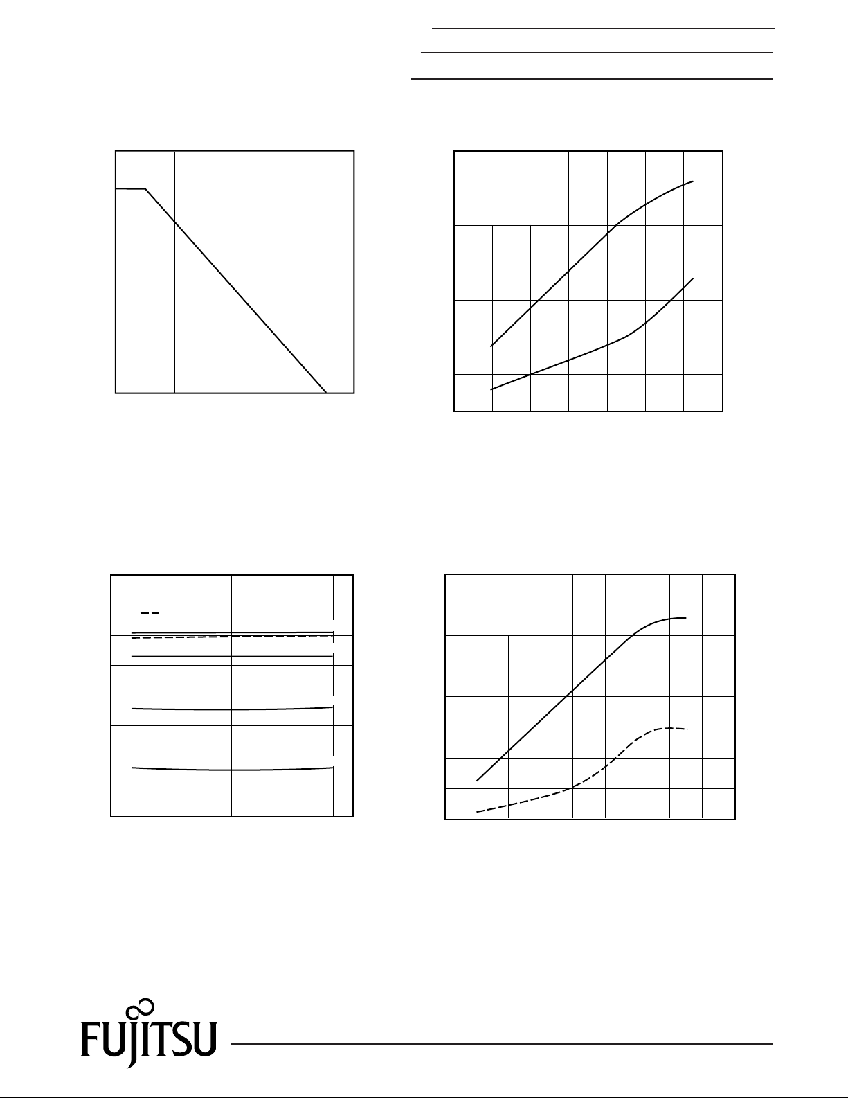
OUTPUT POWER & IM3 vs. INPUT POWER
VDS=10V
f1 = 10.5 GHz
f2 = 10.51 GHz
2-tone test
16 18 20 22 24 26
Input Power (S.C.L.) (dBm)
S.C.L.: Single Carrier Level
27
29
31
33
25
23
-50
-40
-30
-20
Output Power (S.C.L.) (dBm)
IM
3
P
out
IM
3
(dBc)
POWER DERATING CURVE
20
10
40
50
30
0
50 100 150 200
Case Temperature (°C)
Total Power Dissipation (W)
OUTPUT POWER vs. FREQUENCY
9.5
Pin=32dBm
30dBm
28dBm
26dBm
10.510.0
Frequency (GHz)
34
35
36
37
38
39
40
Output Power (dBm)
VDS=10V
P
1dB
OUTPUT POWER vs. INPUT POWER
VDS=10V
f = 10.0 GHz
2420 22 26 28 30 32 34
Input Power (dBm)
30
32
34
36
38
40
28
20
30
40
10
Output Power (dBm)
η
add
P
out
η
add
(%)
Page 3

3
FLM0910-8F
X, Ku-Band Internally Matched FET
S-PARAMETERS
VDS= 10V, IDS= 2200mA
FREQUENCY S11 S21 S12 S22
(MHZ) MAG ANG MAG ANG MAG ANG MAG ANG
9300 .489 132.9 2.699 -108.2 .090 -140.2 .352 66.0
9400 .464 118.8 2.686 -120.0 .092 -152.4 .364 54.7
9500 .451 104.4 2.692 -131.6 .093 -164.8 .377 44.2
9600 .438 90.5 2.657 -142.5 .095 -175.1 .397 35.3
9700 .428 76.7 2.642 -153.9 .096 174.3 .412 28.2
9800 .421 62.4 2.640 -164.8 .095 162.4 .421 21.9
9900 .420 48.0 2.637 -175.5 .100 151.7 .417 17.2
10000 .418 32.1 2.651 173.5 .101 142.3 .406 12.1
10100 .420 15.7 2.668 162.3 .104 130.3 .385 7.9
10200 .424 -2.0 2.689 150.9 .107 119.4 .358 5.2
10300 .428 -20.4 2.703 138.8 .109 108.0 .320 2.6
10400 .440 -39.3 2.703 126.7 .108 96.1 .276 2.6
10500 .452 -58.2 2.691 114.2 .112 84.3 .231 3.3
10600 .469 -76.6 2.656 101.7 .112 72.3 .194 8.4
10700 .484 -94.2 2.600 89.0 .111 61.1 .166 17.4
+j250
+j100
+j50
+j25
+j10
0
-j10
-j25
-j50
-j100
-j250
S
11
S
22
180°
+90°
0°
-90°
S
21
S
12
SCALE FOR |S21|
SCALE FOR |S
12
|
0.2
0.1
250
50Ω
10.7
10.7
9.5
9.5
9.7
9.7
9.9
9.9
10.1
10.1
10.3
10.3
10.5
10.5
10 20
9.3GHz
9.3GHz
82 4 6
10.7
10.7
9.5
9.5
9.7
9.7
9.9
9.9
10.1
10.1
10.3
10.3
10.5
10.5
9.3GHz
9.3GHz
Download S-Parameters, click here
Page 4

4
For further information please contact:
FUJITSU COMPOUND SEMICONDUCTOR, INC.
2355 Zanker Rd.
San Jose, CA 95131-1138, U.S.A.
Phone: (408) 232-9500
FAX: (408) 428-9111
www.fcsi.fujitsu.com
FUJITSU MICROELECTRONICS, LTD.
Compound Semiconductor Division
Network House
Norreys Drive
Maidenhead, Berkshire SL6 4FJ
Phone:+44 (0)1628 504800
FAX:+44 (0)1628 504888
Fujitsu Limited reserves the right to change products and specifications without notice.
The information does not convey any license under rights of Fujitsu Limited or others.
© 1999 FUJITSU COMPOUND SEMICONDUCTOR, INC.
Printed in U.S.A. FCSI0499M200
Fujitsu Compound Semiconductor Products contain gallium arsenide
(GaAs) which can be hazardous to the human body and the environment.
For safety, observe the following procedures:
CAUTION
• Do not put these products into the mouth.
• Do not alter the form of this product into a gas, powder, or liquid
through burning, crushing, or chemical processing as these by-products
are dangerous to the human body if inhaled, ingested, or swallowed.
• Observe government laws and company regulations when discarding this
product. This product must be discarded in accordance with methods
specified by applicable hazardous waste procedures.
FLM0910-8F
X, Ku-Band Internally Matched FET
2-R 1.6±0.15
(0.063)
0.6
(0.024)
10.7
(0.421)
12.0
(0.422)
17.0±0.15
(0.669)
21.0±0.15
(0.827)
12.9±0.2
(0.508)
2.0 Min.
(0.079)
2.0 Min.
(0.079)
0.2 Max.
(0.008)
1.45
(0.059)
Case Style "IB"
Metal-Ceramic Hermetic Package
Unit: mm(inches)
1. Gate
2. Source (Flange)
3. Drain
5.2 Max.
(0.205)
2.6±0.15
(0.102)
0.1
(0.004)
1
2
3
Page 5

 Loading...